EP2846212A1 - Circuit to reduce output capacitor of LDOs - Google Patents
Circuit to reduce output capacitor of LDOs Download PDFInfo
- Publication number
- EP2846212A1 EP2846212A1 EP14183774.0A EP14183774A EP2846212A1 EP 2846212 A1 EP2846212 A1 EP 2846212A1 EP 14183774 A EP14183774 A EP 14183774A EP 2846212 A1 EP2846212 A1 EP 2846212A1
- Authority
- EP
- European Patent Office
- Prior art keywords
- transistor
- current mirror
- gate
- current
- source
- Prior art date
- Legal status (The legal status is an assumption and is not a legal conclusion. Google has not performed a legal analysis and makes no representation as to the accuracy of the status listed.)
- Granted
Links
Images


Classifications
-
- G—PHYSICS
- G05—CONTROLLING; REGULATING
- G05F—SYSTEMS FOR REGULATING ELECTRIC OR MAGNETIC VARIABLES
- G05F1/00—Automatic systems in which deviations of an electric quantity from one or more predetermined values are detected at the output of the system and fed back to a device within the system to restore the detected quantity to its predetermined value or values, i.e. retroactive systems
- G05F1/10—Regulating voltage or current
- G05F1/46—Regulating voltage or current wherein the variable actually regulated by the final control device is DC
- G05F1/56—Regulating voltage or current wherein the variable actually regulated by the final control device is DC using semiconductor devices in series with the load as final control devices
-
- G—PHYSICS
- G05—CONTROLLING; REGULATING
- G05F—SYSTEMS FOR REGULATING ELECTRIC OR MAGNETIC VARIABLES
- G05F3/00—Non-retroactive systems for regulating electric variables by using an uncontrolled element, or an uncontrolled combination of elements, such element or such combination having self-regulating properties
- G05F3/02—Regulating voltage or current
- G05F3/08—Regulating voltage or current wherein the variable is DC
- G05F3/10—Regulating voltage or current wherein the variable is DC using uncontrolled devices with non-linear characteristics
- G05F3/16—Regulating voltage or current wherein the variable is DC using uncontrolled devices with non-linear characteristics being semiconductor devices
- G05F3/20—Regulating voltage or current wherein the variable is DC using uncontrolled devices with non-linear characteristics being semiconductor devices using diode- transistor combinations
- G05F3/26—Current mirrors
- G05F3/262—Current mirrors using field-effect transistors only
-
- H—ELECTRICITY
- H03—ELECTRONIC CIRCUITRY
- H03F—AMPLIFIERS
- H03F1/00—Details of amplifiers with only discharge tubes, only semiconductor devices or only unspecified devices as amplifying elements
- H03F1/08—Modifications of amplifiers to reduce detrimental influences of internal impedances of amplifying elements
- H03F1/083—Modifications of amplifiers to reduce detrimental influences of internal impedances of amplifying elements in transistor amplifiers
- H03F1/086—Modifications of amplifiers to reduce detrimental influences of internal impedances of amplifying elements in transistor amplifiers with FET's
-
- H—ELECTRICITY
- H03—ELECTRONIC CIRCUITRY
- H03F—AMPLIFIERS
- H03F2200/00—Indexing scheme relating to amplifiers
- H03F2200/267—A capacitor based passive circuit, e.g. filter, being used in an amplifying circuit
Definitions
- This disclosure relates generally to electronic circuits and relates in particular output capacitors of Low Drop-Out (LDO) regulators.
- LDO Low Drop-Out
- PCB printed circuit board
- a principal object of the present disclosure is to reduce the size of a decoupling capacitor at the output of an LDO or of an amplifier.
- a further object of the present disclosure is to reduce the footprint for an external decoupling capacitor on PCB.
- a further object of the present disclosure is to improve the phase margin of an LDO.
- a further object of the present disclosure is to reduce gain under low to medium load condition.
- a further object of the present disclosure is to reduction time required for charging and discharging the LDO.
- an object of the present disclosure is to reduce charge required for startup of LDO.
- an object of the present disclosure is to reduce loss of charge when the LDO is disabled.
- a driver circuit for low drop-out regulators or amplifiers allowing reducing a size of an output capacitor while maintaining high stability of the low drop-out regulator (LDO) or of the amplifier within a high range of load current has been achieved.
- LDO low drop-out regulator
- the driver circuit disclosed comprises: a pass transistor connected between a supply voltage and an output node wherein a gate of the pass transistor is controlled by a voltage representing a difference between a reference voltage and an actual output voltage of the LDO, and wherein the gate of the pass transistor is connected in a current mirror configuration to a gate of a first current mirror transistor forming a current mirror, said first current mirror transistor having a smaller size than the pass transistor, wherein the first current mirror transistor is connected between the supply voltage and a first supplemental transistor, said first supplemental transistor having a drain connected to the drain of the first current mirror transistor and a source connected to ground voltage, and a circuitry attached to the current mirror configured to nonlinear mirroring of the load current and capable of allowing reducing small signal impedance at the gate of the pass transistor as the load current increases, hence allowing reducing the size of an output capacitor without compromising stability of the system.
- a method for a driver circuit for low drop-out regulators or amplifiers allowing reducing a size of an output capacitor while maintaining high stability of the low drop-out regulator (LDO) or of the amplifier within a high range of load current, has been achieved.
- the method disclosed comprises the steps of: (1) providing a low drop-out or an amplifier comprising a pass transistor, wherein a gate of the pass transistor is connected in a current mirror configuration to a gate of a first current mirror transistor, and a first supplemental transistor having a drain connected to a drain of the first current mirror transistor, and (2) compensating for increased capacitance at the gate of the pass transistor when the pass transistor is in an active region, at low to medium load currents.
- Fig. 1 shows a simplified schematic for a LDO whose pass transistor P9 is driven by a driver stage N4/ P8.
- the driver stage has P8 in a diode configuration and the current in P8 corresponds to a ratio of the load current. As the load current increases the current in P8 also increases. This increase of the current of P8 increases the transconductance of P8 and thus reduces the impedance at gate of pass transistor P9. The reduction of the impedance at gate of the pass transistor P9 helps to keep the relative position of pole at output node Vout and at gate of P9 constant
- the capacitance seen at gate of P9 changes as the transistor P9 transits from active state (saturated state) to linear region of operation depending on the load current.
- pass transistor P9 is in saturation and there is a small signal gain from node DG to node Vout.
- the pass transistor P9 must also be capable of supplying large currents which relates to a very large device size.
- a large device size relates to a large "gate to drain” capacitance (C gd ). This C gd acts as Miller capacitor and results in a much larger capacitance seen at gate of P9 when P9 is in active region of operation.
- CG ⁇ 9 Cgs P ⁇ 8 + Cgs P ⁇ 9 + Cgd P ⁇ 9 * A out P ⁇ 9 in active / saturation region
- CG ⁇ 9 Cgs P ⁇ 8 + 2 * Cgs P ⁇ 9 P ⁇ 9 in linear / triode region , wherein Aout is small signal gain from node DG to node VOUT, Cgs is gate to source capacitance, and Cgd is gate to drain capacitance.
- One technique would be to increase the transconductance of P8 under low to medium load conditions, which also relates to increase in the current in P8 under low to medium load conditions.
- Fig. 2 shows the modified driver stage of an LDO.
- Transistors P8a and Px are added in parallel to transistor P8 showed in Fig.1 .
- transistor Px is a switch which can be biased with any potential at its gate.
- more branches like P8a and Px can be added in parallel, with different size if needed.
- Px can also be replaced by a resistor. Different Px transistors are used for different branches. Different branches can have different size for P8a and Px.
- Fig. 3 depicts a comparison of phase margins 30 of an LDO with a driver stage according to the circuit of Fig. 1 with phase margins 31 of an LDO with a driver stage according the circuit of Fig. 2 .
- Fig. 3 compares 300mA LDOs having each a 450nF output capacitor.
- Fig. 3 clearly shows that the LDO with the driver stage shown in Fig. 1 has a very small phase margin 30 at low loads, but a considerable improvement is observed for the phase margin 31 of the driver stage shown in Fig. 2 .
- the driver stage of Fig. 1 requires a 4.7uF output capacitor, while the output capacitor of the driver stage of Fig. 2 can be reduced to 1 uF and lower.
- Figs. 4 - 5 show variations of the way to control the gate of Px.
- Fig. 4 illustrates how the gate of Px is controlled by diode connected transistor P1 and current source 11. Depending on the current source 11 the gate potential of transistor Px can be modified. It should be noted that current I1 is independent of the load current.
- the gate of transistor Px is a function of the load current.
- the gate of transistor P1 is connected to node DG.
- current from transistor P1 is by far smaller than current I1 and the gate of Px is pulled to ground.
- the part of the current through P1, which is higher than current I1 flows through diode connected transistor N1 generating the control voltage at gate of Px.
- the gate of Px is a function of the load current. At low loads, current from P1 is far smaller than I1 and gate of Px is pulled to ground. As load current and current through P1 get higher than current I1, the extra current flows through diode connected N1 generating the control voltage at gate of Px.
- Fig. 6 shows a variation of the circuit of Fig. 5 using also transistors P1 and 11 but without transistor N1. Once a current from P1 is higher than the current I1 the gate of Px is pulled to supply and P8a moves from active to deep triode mode. Transistor P1 and the current source I1 form a current comparator.
- Fig. 7 shows a circuit wherein the gate of Px is dynamically biased if the current of current source I2 is higher than the current of current source I1. Once the load current is low, current source I2 is in deep triode mode and the gate of Px is pulled to ground. As the load current increases the potential at DG node decreases and I2 starts to increase till it gets saturated and the part of the I2 current, which is higher than current I1 flows through transistor N1 to generate the biasing potential for gate of Px.
- Fig. 8 shows a variation of the circuit of Fig. 7 without transistor N1. Once the load current at output is large enough to get 12 saturated, the gate of transistor Px is pulled to supply and transistor P8a moves from active to deep triode region of operation. Current source I2 has to be higher than current source I1.
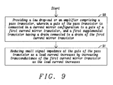
- Fig. 9 shows a flowchart of a method for a driver circuit for low drop-out regulators or amplifiers allowing reducing a size of an output capacitor while maintaining high stability of the low drop-out regulator (LDO) or of the amplifier within a high range of load current.
- a first step 90 depicts provision of a low drop-out or an amplifier comprising a pass transistor, wherein a gate of the pass transistor is connected in a current mirror configuration to a gate of a first current mirror transistor, and a first supplemental transistor having a drain connected to a drain of the first current mirror transistor.
- the next step 91 shows compensating increased capacitance at the gate of the pass transistor occurring as the load current increases. This is performed in the preferred embodiment by reducing small signal impedance of the first current mirror transistor as the load current increases.
- the disclosure teaches nonlinear mirroring of the load current allowing scaling of gain or adapting small signal impedance of the pass transistor depending on other inputs, in case of the preferred embodiment, allowing to reduce small signal impedance at the gate of the pass transistor as the load current increases, hence allowing to reduce the size of an output capacitor without compromising stability of the system.
- the pass transistor need not be PMOS it can be NMOS or BJT or FET as well.
Landscapes
- Engineering & Computer Science (AREA)
- Physics & Mathematics (AREA)
- Electromagnetism (AREA)
- General Physics & Mathematics (AREA)
- Radar, Positioning & Navigation (AREA)
- Automation & Control Theory (AREA)
- Microelectronics & Electronic Packaging (AREA)
- Nonlinear Science (AREA)
- Power Engineering (AREA)
- Amplifiers (AREA)
- Control Of Electrical Variables (AREA)
Abstract
Description
- This application claims priority of
US Provisional Application No. 61/873,904, filed September 5, 2013 - This disclosure relates generally to electronic circuits and relates in particular output capacitors of Low Drop-Out (LDO) regulators.
- In present designs a large external decoupling capacitor is needed at the output of an LDO for increasing the separation between the pole at the output and pole at gate of a pass device under low to medium range of load current.
- A larger capacitor requires a larger footprint on the printed circuit board (PCB) real estate which is very expensive for handheld applications.
- Larger external decoupling capacitors would result in longer time to charge and discharge. If the LDO/ Amplifier is regularly enabled or disabled it would add to loss in charge of battery.
- Disadvantages of present designs are:
- Limited stability
- Output capacitor size
- Large output impedance for driver stage
- Too high gain
- Too much time required to charge and discharge the LDO
- Too much charge required for startup
- Too much charge lost when LDO is disabled
- Too high system boot-up time when LDO is used in a power management integrated circuit (PMIC) together with other LDOs
- Too much time required for testing an IC hosting the LDO
- It is a challenge to designers of LDOs to improve stability of LDOs and to reduce the size of the output capacitor.
- A principal object of the present disclosure is to reduce the size of a decoupling capacitor at the output of an LDO or of an amplifier.
- A further object of the present disclosure is to reduce the footprint for an external decoupling capacitor on PCB.
- A further object of the present disclosure is to improve the phase margin of an LDO.
- A further object of the present disclosure is to reduce gain under low to medium load condition.
- A further object of the present disclosure is to reduction time required for charging and discharging the LDO.
- Furthermore an object of the present disclosure is to reduce charge required for startup of LDO.
- Moreover an object of the present disclosure is to reduce loss of charge when the LDO is disabled.
- In accordance with the objects of this disclosure a driver circuit for low drop-out regulators or amplifiers allowing reducing a size of an output capacitor while maintaining high stability of the low drop-out regulator (LDO) or of the amplifier within a high range of load current has been achieved. The driver circuit disclosed comprises: a pass transistor connected between a supply voltage and an output node wherein a gate of the pass transistor is controlled by a voltage representing a difference between a reference voltage and an actual output voltage of the LDO, and wherein the gate of the pass transistor is connected in a current mirror configuration to a gate of a first current mirror transistor forming a current mirror, said first current mirror transistor having a smaller size than the pass transistor, wherein the first current mirror transistor is connected between the supply voltage and a first supplemental transistor, said first supplemental transistor having a drain connected to the drain of the first current mirror transistor and a source connected to ground voltage, and a circuitry attached to the current mirror configured to nonlinear mirroring of the load current and capable of allowing reducing small signal impedance at the gate of the pass transistor as the load current increases, hence allowing reducing the size of an output capacitor without compromising stability of the system.
- In accordance with the objects of this disclosure a method for a driver circuit for low drop-out regulators or amplifiers, allowing reducing a size of an output capacitor while maintaining high stability of the low drop-out regulator (LDO) or of the amplifier within a high range of load current, has been achieved. The method disclosed comprises the steps of: (1) providing a low drop-out or an amplifier comprising a pass transistor, wherein a gate of the pass transistor is connected in a current mirror configuration to a gate of a first current mirror transistor, and a first supplemental transistor having a drain connected to a drain of the first current mirror transistor, and (2) compensating for increased capacitance at the gate of the pass transistor when the pass transistor is in an active region, at low to medium load currents.
- In the accompanying drawings forming a material part of this description, there is shown:
-
Fig. 1 shows a simplified schematic of the LDO whose pass transistor id driven by a driver stage. -
Fig. 2 shows a modified driver stage of an LDO. -
Fig. 3 depicts a comparison of phase margins of an LDO with a driver stage according to the circuit ofFig. 1 with an LDO with a driver stage according the circuit ofFig. 2 . -
Fig. 4 illustrates how the gate of transistor Px is controlled by a diode connected transistor P1 andcurrent source 11. -
Fig. 5 depicts how the gate of transistor Px is a function of the load current. -
Fig. 6 shows a variation of the circuit ofFig. 5 using also transistors P1 and 11 but without transistor N1. -
Fig. 7 shows a circuit wherein the gate of Px is dynamically biased. -
Fig. 8 shows a variation of the circuit ofFig. 7 . -
Fig. 9 shows a flowchart of a method for a driver circuit for low drop-out regulators or amplifiers allowing reducing a size of an output capacitor while maintaining high stability of the low drop-out regulator (LDO) or of the amplifier within a high range of load current. - Disclosed are embodiments of drive stages of LDO's. It should be noted that the drive stages could be used for amplifiers as well.
-
Fig. 1 shows a simplified schematic for a LDO whose pass transistor P9 is driven by a driver stage N4/ P8. The small signal impedance R seen at gate of pass device P9 is given by following equation:
- The driver stage has P8 in a diode configuration and the current in P8 corresponds to a ratio of the load current. As the load current increases the current in P8 also increases. This increase of the current of P8 increases the transconductance of P8 and thus reduces the impedance at gate of pass transistor P9. The reduction of the impedance at gate of the pass transistor P9 helps to keep the relative position of pole at output node Vout and at gate of P9 constant
- It has to be noted that in practice the capacitance seen at gate of P9 changes as the transistor P9 transits from active state (saturated state) to linear region of operation depending on the load current. For small currents at the output, pass transistor P9 is in saturation and there is a small signal gain from node DG to node Vout. The pass transistor P9 must also be capable of supplying large currents which relates to a very large device size. A large device size relates to a large "gate to drain" capacitance (Cgd). This Cgd acts as Miller capacitor and results in a much larger capacitance seen at gate of P9 when P9 is in active region of operation.
- The equations below give an approximate capacitance CG9 seen at gate of P9 under different region of operation, which in turn depend the current load at node Vout.
- The following equations are valid for the capacitance CG9 depending on different current load at the output node Vout:


wherein Aout is small signal gain from node DG to node VOUT, Cgs is gate to source capacitance, and Cgd is gate to drain capacitance. - The increased capacitance CG9 at gate of P9 in active region does not allow maintaining a constant separation between the pole at Vout and DG. Load current for which P9 is in active region of operation results in lower phase margin of the system and could make the system unstable. To compensate for this a larger capacitor is needed at the output of the LDO.
- One technique would be to increase the transconductance of P8 under low to medium load conditions, which also relates to increase in the current in P8 under low to medium load conditions.
- The circuit of
Fig. 2 shows the modified driver stage of an LDO. Transistors P8a and Px are added in parallel to transistor P8 showed inFig.1 . It should be noted that more than one transistor P8a could be deployed in parallel and transistor Px is a switch which can be biased with any potential at its gate. As required by design, more branches like P8a and Px can be added in parallel, with different size if needed. Px can also be replaced by a resistor. Different Px transistors are used for different branches. Different branches can have different size for P8a and Px. - Under low load and medium load condition P8a is in active region of operation i.e. VdsP8a>VgsP8a-VthP8a. This means the small signal impedance seen at gate of transistor P9 is follows:

- Depending on sizes of P8a and Px the small signal impedance R can be modified as required by design. Reduction of R as seen at gate of P9 compensates the increased capacitance seen at gate of P9 when P9 is in active region of operation
As load increases P8a transits from active region to deep triode region as the voltage drop across Px increases and the impedance R seen at gate of P9 reduces back to
-
Fig. 3 depicts a comparison ofphase margins 30 of an LDO with a driver stage according to the circuit ofFig. 1 withphase margins 31 of an LDO with a driver stage according the circuit ofFig. 2 . As a non-limiting exampleFig. 3 compares 300mA LDOs having each a 450nF output capacitor. -
Fig. 3 clearly shows that the LDO with the driver stage shown inFig. 1 has a verysmall phase margin 30 at low loads, but a considerable improvement is observed for thephase margin 31 of the driver stage shown inFig. 2 . The driver stage ofFig. 1 requires a 4.7uF output capacitor, while the output capacitor of the driver stage ofFig. 2 can be reduced to 1 uF and lower. -
Figs. 4 - 5 show variations of the way to control the gate of Px. -
Fig. 4 illustrates how the gate of Px is controlled by diode connected transistor P1 andcurrent source 11. Depending on thecurrent source 11 the gate potential of transistor Px can be modified. It should be noted that current I1 is independent of the load current. - In
Fig. 5 the gate of transistor Px is a function of the load current. The gate of transistor P1 is connected to node DG. At low loads current from transistor P1 is by far smaller than current I1 and the gate of Px is pulled to ground. As load current and subsequently current through P1 get higher than current I1, the part of the current through P1, which is higher than current I1 flows through diode connected transistor N1 generating the control voltage at gate of Px. In the circuit ofFig. 5 the gate of Px is a function of the load current. At low loads, current from P1 is far smaller than I1 and gate of Px is pulled to ground. As load current and current through P1 get higher than current I1, the extra current flows through diode connected N1 generating the control voltage at gate of Px. -
Fig. 6 shows a variation of the circuit ofFig. 5 using also transistors P1 and 11 but without transistor N1. Once a current from P1 is higher than the current I1 the gate of Px is pulled to supply and P8a moves from active to deep triode mode. Transistor P1 and the current source I1 form a current comparator. -
Fig. 7 shows a circuit wherein the gate of Px is dynamically biased if the current of current source I2 is higher than the current of current source I1. Once the load current is low, current source I2 is in deep triode mode and the gate of Px is pulled to ground. As the load current increases the potential at DG node decreases and I2 starts to increase till it gets saturated and the part of the I2 current, which is higher than current I1 flows through transistor N1 to generate the biasing potential for gate of Px. -
Fig. 8 shows a variation of the circuit ofFig. 7 without transistor N1. Once the load current at output is large enough to get 12 saturated, the gate of transistor Px is pulled to supply and transistor P8a moves from active to deep triode region of operation. Current source I2 has to be higher than current source I1. -
Fig. 9 shows a flowchart of a method for a driver circuit for low drop-out regulators or amplifiers allowing reducing a size of an output capacitor while maintaining high stability of the low drop-out regulator (LDO) or of the amplifier within a high range of load current. Afirst step 90 depicts provision of a low drop-out or an amplifier comprising a pass transistor, wherein a gate of the pass transistor is connected in a current mirror configuration to a gate of a first current mirror transistor, and a first supplemental transistor having a drain connected to a drain of the first current mirror transistor. Thenext step 91 shows compensating increased capacitance at the gate of the pass transistor occurring as the load current increases. This is performed in the preferred embodiment by reducing small signal impedance of the first current mirror transistor as the load current increases. - In summary, the disclosure teaches nonlinear mirroring of the load current allowing scaling of gain or adapting small signal impedance of the pass transistor depending on other inputs, in case of the preferred embodiment, allowing to reduce small signal impedance at the gate of the pass transistor as the load current increases, hence allowing to reduce the size of an output capacitor without compromising stability of the system. Furthermore it should be noted that the pass transistor need not be PMOS it can be NMOS or BJT or FET as well.
- While the disclosure has been particularly shown and described with reference to the preferred embodiments thereof, it will be understood by those skilled in the art that various changes in form and details may be made without departing from the spirit and scope of the disclosure.
Claims (19)
- A driver circuit for low drop-out regulators or amplifiers allowing reducing a size of an output capacitor while maintaining high stability of the low drop-out regulator (LDO) or of the amplifier within a high range of load current, comprising:- a pass transistor connected between a supply voltage and an output node wherein a gate of the pass transistor is controlled by a voltage representing a difference between a reference voltage and an actual output voltage of the LDO, and wherein the gate of the pass transistor is connected in a current mirror configuration to a gate of a first current mirror transistor forming a current mirror;- said first current mirror transistor having a smaller size than the pass transistor, wherein the first current mirror transistor is connected between the supply voltage and a first supplemental transistor;- said first supplemental transistor having a drain connected to the drain of the first current mirror transistor and a source connected to ground voltage; and- a circuitry attached to the current mirror configured to nonlinear mirroring of the load current and capable of allowing reducing small signal impedance at the gate of the pass transistor as the load current increases, hence allowing reducing the size of an output capacitor without compromising stability of the system.
- The driver circuit of claim 1, wherein the circuitry attached comprises a first circuit branch comprising a second current mirror transistor, which is deployed in a current mirror configuration in parallel to the first current mirror transistor, and a resistive means, wherein a first terminal of the resistive means is connected to the second current mirror transistor and a second terminal of the resistive means is connected to a node between the first current mirror transistor and the supplemental transistor.
- The driver circuit of claim 2, wherein said resistive means is a resistor or a transistor.
- The driver circuit of claim 2, wherein additional branches are deployed in parallel to the first branch, wherein each branch comprises a current mirror transistor in parallel to the first current mirror transistor, and a resistive means, wherein a first terminal of the resistive means is connected to the current mirror transistor of the correspondent branch and a second terminal of the resistive means is connected to a node between the first current mirror transistor and the supplemental transistor.
- The driver circuit of claim 1, wherein the circuitry attached comprises a first circuit branch comprising a second current mirror transistor, which is deployed in a current mirror configuration in parallel to the first current mirror transistor, and a transistor Px, wherein a source of the transistor PX is connected to a drain of the second current mirror transistor and a drain of the transistor Px is connected to a node between the first current mirror transistor and the supplemental transistor and wherein a gate of the transistor Px is controlled by a diode connected transistor P1 and by a current source I1, wherein a source of transistor P1 is connected to a supply voltage of the driver circuit and a drain of transistor P1 is connected to the gate of transistor PX and to first terminal of the current source I1, wherein a second terminal of the current source I1 is connected to ground.
- The driver circuit of claim 1, wherein the circuitry attached comprises a first circuit branch comprising a second current mirror transistor, which is deployed in a current mirror configuration in parallel to the first current mirror transistor, and a transistor Px, wherein a source of the transistor PX is connected to a drain of the second current mirror transistor and a drain of the transistor Px is connected to a node between the first current mirror transistor and the supplemental transistor, wherein a gate voltage of the transistor Px is configured to be dependent on the load current of the pass transistor wherein the gate voltage of transistor Px is controlled by transistor P1, diode connected transistor N1, and by a current source I1, wherein a gate of transistor P1 is connected to the gate of the pass transistor, a source of transistor P1 is connected to a supply voltage of the driver circuit and a drain of transistor P1 is connected to the gate of transistor PX, to a first terminal of the current source I1, and to a drain and a gate of the transistor N1, wherein a second terminal of the current source I1 and a source of transistor N1 are connected to ground.
- The driver circuit of claim 1, wherein the circuitry attached comprises a first circuit branch comprising a second current mirror transistor, which is deployed in a current mirror configuration in parallel to the first current mirror transistor, and a transistor Px, wherein a source of the transistor PX is connected to a drain of the second current mirror transistor and a drain of the transistor Px is connected to a node between the first current mirror transistor and the supplemental transistor, wherein a gate voltage of the transistor Px is configured to be dependent on the load current of the pass transistor wherein the gate voltage of transistor Px is controlled by transistor P1 and by a current source I1, wherein a gate of transistor P1 is connected to the gate of the pass transistor, a source of transistor P1 is connected to a supply voltage of the driver circuit and a drain of transistor P1 is connected to the gate of transistor PX and to a first terminal of the current source I1, wherein a second terminal of the current source I1 is connected to ground.
- The driver circuit of claim 1, wherein the circuitry attached comprises a first circuit branch comprising a second current mirror transistor, which is deployed in a current mirror configuration in parallel to the first current mirror transistor, and a transistor Px, wherein a source of the transistor PX is connected to a drain of the second current mirror transistor and a drain of the transistor Px is connected to a node between the first current mirror transistor and the supplemental transistor, wherein a gate voltage of the transistor Px is configured to be dynamically biased, wherein the gate voltage of transistor Px is controlled by transistor P1, diode connected transistor N1, and by a current source I1, wherein a gate of transistor P1 is connected to the gate of the pass transistor, a source of transistor P1 is connected to second terminal of a current source I2, wherein a first terminal of the current source I2 is connect to a supply voltage of the driver circuit and a drain of transistor P1 is connected to the gate of transistor PX, to a first terminal of the current source I1, and to a drain and a gate of the transistor N1, wherein a second terminal of the current source I1 and a source of transistor N1 are connected to ground.
- The driver circuit of claim 1, wherein the circuitry attached comprises a first circuit branch comprising a second current mirror transistor, which is deployed in a current mirror configuration in parallel to the first current mirror transistor, and a transistor Px, wherein a source of the transistor PX is connected to a drain of the second current mirror transistor and a drain of the transistor Px is connected to a node between the first current mirror transistor and the supplemental transistor, wherein a gate voltage of the transistor Px is configured to be dynamically biased, wherein the gate voltage of transistor Px is controlled by transistor P1 and by a current source I1, wherein a gate of transistor P1 is connected to the gate of the pass transistor, a source of transistor P1 is connected to second terminal of a current source I2, wherein a first terminal of the current source I2 is connect to a supply voltage of the driver circuit and a drain of transistor P1 is connected to the gate of transistor PX, to a first terminal of the current source I1, wherein a second terminal of the current source I1 is connected to ground.
- A method for a driver circuit for low drop-out regulators or amplifiers allowing reducing a size of an output capacitor while maintaining high stability of the low drop-out regulator (LDO) or of the amplifier within a high range of load current comprising the steps of:(1) providing a low drop-out or an amplifier comprising a pass transistor, wherein a gate of the pass transistor is connected in a current mirror configuration to a gate of a first current mirror transistor, and a first supplemental transistor having a drain connected to a drain of the first current mirror transistor; and(2) compensating for increased capacitance at the gate of the pass transistor when the pass transistor is in an active region, at low to medium load currents.
- The method of claim 10, wherein said capacitance at the gate of the pass transistor is compensated by a circuitry attached configured to reducing small signal impedance of the first current mirror transistor as the load current increases.
- The method of claim 11, wherein the small signal impedance of the first current mirror transistor is reduced by a circuitry attached to the current mirror configured to nonlinear mirroring of the load current and reducing small signal impedance at the gate of the pass transistor as the load current increases, hence allowing reducing the size of an output capacitor without compromising stability of the system.
- The method of claim 12, wherein the circuitry attached comprises a first circuit branch comprising a second current mirror transistor, which is deployed in a current mirror configuration in parallel to the first current mirror transistor, and a resistive means, wherein a first terminal of the resistive means is connected to the second current mirror transistor and a second terminal of the resistive means is connected to a node between the first current mirror transistor and the supplemental transistor.
- The method of claim 13, wherein additional branches are deployed in parallel to the first branch, wherein each branch comprises a current mirror transistor in parallel to the first current mirror transistor, and a resistive means, wherein a first terminal of the resistive means is connected to the current mirror transistor of the correspondent branch and a second terminal of the resistive means is connected to a node between the first current mirror transistor and the supplemental transistor.
- The method of claim 11, wherein the circuitry attached comprises a first circuit branch comprising a second current mirror transistor, which is deployed in a current mirror configuration in parallel to the first current mirror transistor, and a transistor Px, wherein a source of the transistor PX is connected to a drain of the second current mirror transistor and a drain of the transistor Px is connected to a node between the first current mirror transistor and the supplemental transistor and wherein a gate of the transistor Px is controlled by a diode connected transistor P1 and by a current source I1, wherein a source of transistor P1 is connected to a supply voltage of the driver circuit and a drain of transistor P1 is connected to the gate of transistor PX and to first terminal of the current source I1, wherein a second terminal of the current source I1 is connected to ground.
- The method of claim 11, wherein the circuitry attached comprises a first circuit branch comprising a second current mirror transistor, which is deployed in a current mirror configuration in parallel to the first current mirror transistor, and a transistor Px, wherein a source of the transistor PX is connected to a drain of the second current mirror transistor and a drain of the transistor Px is connected to a node between the first current mirror transistor and the supplemental transistor, wherein a gate voltage of the transistor Px is configured to be dependent on the load current of the pass transistor wherein the gate voltage of transistor Px is controlled by transistor P1, diode connected transistor N1, and by a current source I1, wherein a gate of transistor P1 is connected to the gate of the pass transistor, a source of transistor P1 is connected to a supply voltage of the driver circuit and a drain of transistor P1 is connected to the gate of transistor PX, to a first terminal of the current source I1, and to a drain and a gate of the transistor N1, wherein a second terminal of the current source I1 and a source of transistor N1 are connected to ground.
- The method of claim 11, wherein the circuitry attached comprises a first circuit branch comprising a second current mirror transistor, which is deployed in a current mirror configuration in parallel to the first current mirror transistor, and a transistor Px, wherein a source of the transistor PX is connected to a drain of the second current mirror transistor and a drain of the transistor Px is connected to a node between the first current mirror transistor and the supplemental transistor, wherein a gate voltage of the transistor Px is configured to be dependent on the load current of the pass transistor wherein the gate voltage of transistor Px is controlled by transistor P1 and by a current source I1, wherein a gate of transistor P1 is connected to the gate of the pass transistor, a source of transistor P1 is connected to a supply voltage of the driver circuit and a drain of transistor.
- The method of claim 11, wherein the circuitry attached comprises a first circuit branch comprising a second current mirror transistor, which is deployed in a current mirror configuration in parallel to the first current mirror transistor, and a transistor Px, wherein a source of the transistor PX is connected to a drain of the second current mirror transistor and a drain of the transistor Px is connected to a node between the first current mirror transistor and the supplemental transistor, wherein a gate voltage of the transistor Px is configured to be dynamically biased, wherein the gate voltage of transistor Px is controlled by transistor P1, diode connected transistor N1, and by a current source I1, wherein a gate of transistor P1 is connected to the gate of the pass transistor, a source of transistor P1 is connected to second terminal of a current source I2, wherein a first terminal of the current source I2 is connect to a supply voltage of the driver circuit and a drain of transistor P1 is connected to the gate of transistor PX, to a first terminal of the current source I1, and to a drain and a gate of the transistor N1, wherein a second terminal of the current source I1 and a source of transistor N1 are connected to ground.
- The method of claim 11, wherein the circuitry attached comprises a first circuit branch comprising a second current mirror transistor, which is deployed in a current mirror configuration in parallel to the first current mirror transistor, and a transistor Px, wherein a source of the transistor PX is connected to a drain of the second current mirror transistor and a drain of the transistor Px is connected to a node between the first current mirror transistor and the supplemental transistor, wherein a gate voltage of the transistor Px is configured to be dynamically biased, wherein the gate voltage of transistor Px is controlled by transistor P1 and by a current source I1, wherein a gate of transistor P1 is connected to the gate of the pass transistor, a source of transistor P1 is connected to second terminal of a current source I2, wherein a first terminal of the current source I2 is connect to a supply voltage of the driver circuit and a drain of transistor P1 is connected to the gate of transistor PX, to a first terminal of the current source I1, wherein a second terminal of the current source I1 is connected to ground.
Applications Claiming Priority (1)
| Application Number | Priority Date | Filing Date | Title |
|---|---|---|---|
| US201361873904P | 2013-09-05 | 2013-09-05 |
Publications (2)
| Publication Number | Publication Date |
|---|---|
| EP2846212A1 true EP2846212A1 (en) | 2015-03-11 |
| EP2846212B1 EP2846212B1 (en) | 2019-04-03 |
Family
ID=51483355
Family Applications (1)
| Application Number | Title | Priority Date | Filing Date |
|---|---|---|---|
| EP14183774.0A Active EP2846212B1 (en) | 2013-09-05 | 2014-09-05 | Circuit to reduce output capacitor of LDOs |
Country Status (2)
| Country | Link |
|---|---|
| US (1) | US9395731B2 (en) |
| EP (1) | EP2846212B1 (en) |
Cited By (1)
| Publication number | Priority date | Publication date | Assignee | Title |
|---|---|---|---|---|
| US20200012303A1 (en) * | 2018-07-09 | 2020-01-09 | Stichting Imec Nederland | Low dropout voltage regulator, a supply voltage circuit and a method for generating a clean supply voltage |
Families Citing this family (11)
| Publication number | Priority date | Publication date | Assignee | Title |
|---|---|---|---|---|
| DE102014013032A1 (en) * | 2014-09-02 | 2016-03-03 | Infineon Technologies Ag | Generation of a current with reverse supply voltage proportionality |
| GB2539457A (en) * | 2015-06-16 | 2016-12-21 | Nordic Semiconductor Asa | Voltage regulators |
| DE102015218656B4 (en) | 2015-09-28 | 2021-03-25 | Dialog Semiconductor (Uk) Limited | Linear regulator with improved supply voltage penetration |
| US9740225B1 (en) * | 2016-02-24 | 2017-08-22 | Avago Technologies General Ip (Singapore) Pte. Ltd. | Low dropout regulator with replica feedback frequency compensation |
| EP3246784B1 (en) * | 2016-05-19 | 2020-01-01 | NXP USA, Inc. | A compensation circuit |
| US11209848B2 (en) | 2016-06-07 | 2021-12-28 | Analog Devices International Unlimited Company | Fast regulator architecture having transistor helper |
| EP3951551B1 (en) * | 2020-08-07 | 2023-02-22 | Scalinx | Voltage regulator and method |
| US12166417B2 (en) * | 2021-12-17 | 2024-12-10 | Qualcomm Incorporated | Nonlinear current mirror for fast transient and low power regulator |
| US11616505B1 (en) * | 2022-02-17 | 2023-03-28 | Qualcomm Incorporated | Temperature-compensated low-pass filter |
| CN115756059A (en) * | 2022-11-28 | 2023-03-07 | 佛山科学技术学院 | Quick transient response low dropout regulator circuit |
| CN119902588B (en) * | 2024-12-18 | 2025-09-30 | 晶艺半导体有限公司 | Low-dropout linear voltage stabilizing circuit |
Citations (2)
| Publication number | Priority date | Publication date | Assignee | Title |
|---|---|---|---|---|
| US20120182167A1 (en) * | 2011-01-14 | 2012-07-19 | Analog Devices, Inc. | Buffer to drive reference voltage |
| US20130147447A1 (en) * | 2011-12-12 | 2013-06-13 | Dialog Semiconductor Gmbh | High-Speed LDO Driver Circuit using Adaptive Impedance Control |
Family Cites Families (7)
| Publication number | Priority date | Publication date | Assignee | Title |
|---|---|---|---|---|
| US6977490B1 (en) * | 2002-12-23 | 2005-12-20 | Marvell International Ltd. | Compensation for low drop out voltage regulator |
| TWI300170B (en) * | 2005-09-13 | 2008-08-21 | Ind Tech Res Inst | Low-dropout voltage regulator |
| CN101038497B (en) * | 2006-03-17 | 2010-09-29 | 深圳赛意法微电子有限公司 | Compensation method, compensated regulator and electronic circuit |
| US7843180B1 (en) * | 2008-04-11 | 2010-11-30 | Lonestar Inventions, L.P. | Multi-stage linear voltage regulator with frequency compensation |
| KR101036923B1 (en) * | 2009-12-30 | 2011-05-25 | 주식회사 하이닉스반도체 | Semiconductor memory device |
| EP2520998A1 (en) * | 2011-05-03 | 2012-11-07 | Dialog Semiconductor GmbH | Flexible load current dependent feedback compensation for linear regulators utilizing ultra-low bypass capacitances |
| FR2988869A1 (en) * | 2012-04-03 | 2013-10-04 | St Microelectronics Rousset | LOW VOLTAGE DROP REGULATOR WITH IMPROVED OUTPUT STAGE |
-
2014
- 2014-09-04 US US14/477,079 patent/US9395731B2/en active Active
- 2014-09-05 EP EP14183774.0A patent/EP2846212B1/en active Active
Patent Citations (2)
| Publication number | Priority date | Publication date | Assignee | Title |
|---|---|---|---|---|
| US20120182167A1 (en) * | 2011-01-14 | 2012-07-19 | Analog Devices, Inc. | Buffer to drive reference voltage |
| US20130147447A1 (en) * | 2011-12-12 | 2013-06-13 | Dialog Semiconductor Gmbh | High-Speed LDO Driver Circuit using Adaptive Impedance Control |
Non-Patent Citations (2)
| Title |
|---|
| MIN TAN: "A zero-ESR stable adaptively biased low-dropout regulator in standard CMOS technology", ASIC, 2009. ASICON '09. IEEE 8TH INTERNATIONAL CONFERENCE ON, IEEE, PISCATAWAY, NJ, USA, 20 October 2009 (2009-10-20), pages 1185 - 1188, XP031578781, ISBN: 978-1-4244-3868-6 * |
| YONGGEN LIU ET AL: "A chip-area-efficient CMOS low-dropout regulator using wide-swing voltage buffer with parabolic adaptive biasing for portable applications", IPEC, 2012 CONFERENCE PROCEEDINGS, IEEE, 12 December 2012 (2012-12-12), pages 233 - 236, XP032415920, ISBN: 978-1-4673-4582-8, DOI: 10.1109/IPEC.2012.6522668 * |
Cited By (2)
| Publication number | Priority date | Publication date | Assignee | Title |
|---|---|---|---|---|
| US20200012303A1 (en) * | 2018-07-09 | 2020-01-09 | Stichting Imec Nederland | Low dropout voltage regulator, a supply voltage circuit and a method for generating a clean supply voltage |
| EP3594772A1 (en) * | 2018-07-09 | 2020-01-15 | Stichting IMEC Nederland | A low dropout voltage regulator, a supply voltage circuit and a method for generating a clean supply voltage |
Also Published As
| Publication number | Publication date |
|---|---|
| EP2846212B1 (en) | 2019-04-03 |
| US20150061772A1 (en) | 2015-03-05 |
| US9395731B2 (en) | 2016-07-19 |
Similar Documents
| Publication | Publication Date | Title |
|---|---|---|
| US9395731B2 (en) | Circuit to reduce output capacitor of LDOs | |
| US10296029B2 (en) | Method for adaptive compensation of linear voltage regulators | |
| KR102247122B1 (en) | Voltage regulator and electronic apparatus | |
| CN108021177B (en) | NMOS-based voltage regulator | |
| US10248144B2 (en) | Linear regulator device with relatively low static power consumption | |
| US9740221B2 (en) | Method to limit the inrush current in large output capacitance LDO's | |
| US9052729B2 (en) | Current control for output device biasing stage | |
| EP2857923A1 (en) | An apparatus and method for a voltage regulator with improved output voltage regulated loop biasing | |
| CN205092772U (en) | Linear regulator control circuit | |
| US9367074B2 (en) | Voltage regulator capable of stabilizing an output voltage even when a power supply fluctuates | |
| CN101604174B (en) | Voltage regulator | |
| KR20150111301A (en) | Voltage regulator | |
| CN104699153A (en) | Low-dropout linear regulator | |
| CN111857230A (en) | Linear regulator and electronic device | |
| US9160230B2 (en) | DC/DC converter and electronic apparatus | |
| US7863969B2 (en) | Power supply voltage dropping circuit using an N-channel transistor output stage | |
| US10156861B2 (en) | Low-dropout regulator with pole-zero tracking frequency compensation | |
| US10291163B2 (en) | Cascode structure for linear regulators and clamps | |
| US20060103361A1 (en) | Linear voltage regulator | |
| US9367073B2 (en) | Voltage regulator | |
| EP2759899A1 (en) | Clean startup and power saving in pulsed enabling of LDO | |
| US8253479B2 (en) | Output driver circuits for voltage regulators | |
| US20050218993A1 (en) | Fast-response current limiting | |
| KR20160012858A (en) | Low dropout regulator | |
| CN215117306U (en) | A Power-Saving and Area-Saving Soft-Start Circuit Used in LDOs |
Legal Events
| Date | Code | Title | Description |
|---|---|---|---|
| 17P | Request for examination filed |
Effective date: 20140905 |
|
| AK | Designated contracting states |
Kind code of ref document: A1 Designated state(s): AL AT BE BG CH CY CZ DE DK EE ES FI FR GB GR HR HU IE IS IT LI LT LU LV MC MK MT NL NO PL PT RO RS SE SI SK SM TR |
|
| AX | Request for extension of the european patent |
Extension state: BA ME |
|
| PUAI | Public reference made under article 153(3) epc to a published international application that has entered the european phase |
Free format text: ORIGINAL CODE: 0009012 |
|
| R17P | Request for examination filed (corrected) |
Effective date: 20150910 |
|
| RBV | Designated contracting states (corrected) |
Designated state(s): AL AT BE BG CH CY CZ DE DK EE ES FI FR GB GR HR HU IE IS IT LI LT LU LV MC MK MT NL NO PL PT RO RS SE SI SK SM TR |
|
| GRAP | Despatch of communication of intention to grant a patent |
Free format text: ORIGINAL CODE: EPIDOSNIGR1 |
|
| STAA | Information on the status of an ep patent application or granted ep patent |
Free format text: STATUS: GRANT OF PATENT IS INTENDED |
|
| RIC1 | Information provided on ipc code assigned before grant |
Ipc: H03F 1/08 20060101ALI20180925BHEP Ipc: G05F 3/26 20060101ALI20180925BHEP Ipc: G05F 1/56 20060101AFI20180925BHEP |
|
| INTG | Intention to grant announced |
Effective date: 20181018 |
|
| GRAS | Grant fee paid |
Free format text: ORIGINAL CODE: EPIDOSNIGR3 |
|
| GRAA | (expected) grant |
Free format text: ORIGINAL CODE: 0009210 |
|
| STAA | Information on the status of an ep patent application or granted ep patent |
Free format text: STATUS: THE PATENT HAS BEEN GRANTED |
|
| AK | Designated contracting states |
Kind code of ref document: B1 Designated state(s): AL AT BE BG CH CY CZ DE DK EE ES FI FR GB GR HR HU IE IS IT LI LT LU LV MC MK MT NL NO PL PT RO RS SE SI SK SM TR |
|
| REG | Reference to a national code |
Ref country code: GB Ref legal event code: FG4D |
|
| REG | Reference to a national code |
Ref country code: CH Ref legal event code: EP Ref country code: AT Ref legal event code: REF Ref document number: 1116518 Country of ref document: AT Kind code of ref document: T Effective date: 20190415 |
|
| REG | Reference to a national code |
Ref country code: DE Ref legal event code: R096 Ref document number: 602014043915 Country of ref document: DE |
|
| REG | Reference to a national code |
Ref country code: IE Ref legal event code: FG4D |
|
| REG | Reference to a national code |
Ref country code: NL Ref legal event code: MP Effective date: 20190403 |
|
| REG | Reference to a national code |
Ref country code: LT Ref legal event code: MG4D |
|
| REG | Reference to a national code |
Ref country code: AT Ref legal event code: MK05 Ref document number: 1116518 Country of ref document: AT Kind code of ref document: T Effective date: 20190403 |
|
| PG25 | Lapsed in a contracting state [announced via postgrant information from national office to epo] |
Ref country code: NL Free format text: LAPSE BECAUSE OF FAILURE TO SUBMIT A TRANSLATION OF THE DESCRIPTION OR TO PAY THE FEE WITHIN THE PRESCRIBED TIME-LIMIT Effective date: 20190403 |
|
| PG25 | Lapsed in a contracting state [announced via postgrant information from national office to epo] |
Ref country code: CZ Free format text: LAPSE BECAUSE OF FAILURE TO SUBMIT A TRANSLATION OF THE DESCRIPTION OR TO PAY THE FEE WITHIN THE PRESCRIBED TIME-LIMIT Effective date: 20190403 Ref country code: NO Free format text: LAPSE BECAUSE OF FAILURE TO SUBMIT A TRANSLATION OF THE DESCRIPTION OR TO PAY THE FEE WITHIN THE PRESCRIBED TIME-LIMIT Effective date: 20190703 Ref country code: LT Free format text: LAPSE BECAUSE OF FAILURE TO SUBMIT A TRANSLATION OF THE DESCRIPTION OR TO PAY THE FEE WITHIN THE PRESCRIBED TIME-LIMIT Effective date: 20190403 Ref country code: ES Free format text: LAPSE BECAUSE OF FAILURE TO SUBMIT A TRANSLATION OF THE DESCRIPTION OR TO PAY THE FEE WITHIN THE PRESCRIBED TIME-LIMIT Effective date: 20190403 Ref country code: SE Free format text: LAPSE BECAUSE OF FAILURE TO SUBMIT A TRANSLATION OF THE DESCRIPTION OR TO PAY THE FEE WITHIN THE PRESCRIBED TIME-LIMIT Effective date: 20190403 Ref country code: HR Free format text: LAPSE BECAUSE OF FAILURE TO SUBMIT A TRANSLATION OF THE DESCRIPTION OR TO PAY THE FEE WITHIN THE PRESCRIBED TIME-LIMIT Effective date: 20190403 Ref country code: PT Free format text: LAPSE BECAUSE OF FAILURE TO SUBMIT A TRANSLATION OF THE DESCRIPTION OR TO PAY THE FEE WITHIN THE PRESCRIBED TIME-LIMIT Effective date: 20190803 Ref country code: AL Free format text: LAPSE BECAUSE OF FAILURE TO SUBMIT A TRANSLATION OF THE DESCRIPTION OR TO PAY THE FEE WITHIN THE PRESCRIBED TIME-LIMIT Effective date: 20190403 Ref country code: FI Free format text: LAPSE BECAUSE OF FAILURE TO SUBMIT A TRANSLATION OF THE DESCRIPTION OR TO PAY THE FEE WITHIN THE PRESCRIBED TIME-LIMIT Effective date: 20190403 |
|
| PG25 | Lapsed in a contracting state [announced via postgrant information from national office to epo] |
Ref country code: RS Free format text: LAPSE BECAUSE OF FAILURE TO SUBMIT A TRANSLATION OF THE DESCRIPTION OR TO PAY THE FEE WITHIN THE PRESCRIBED TIME-LIMIT Effective date: 20190403 Ref country code: LV Free format text: LAPSE BECAUSE OF FAILURE TO SUBMIT A TRANSLATION OF THE DESCRIPTION OR TO PAY THE FEE WITHIN THE PRESCRIBED TIME-LIMIT Effective date: 20190403 Ref country code: GR Free format text: LAPSE BECAUSE OF FAILURE TO SUBMIT A TRANSLATION OF THE DESCRIPTION OR TO PAY THE FEE WITHIN THE PRESCRIBED TIME-LIMIT Effective date: 20190704 Ref country code: PL Free format text: LAPSE BECAUSE OF FAILURE TO SUBMIT A TRANSLATION OF THE DESCRIPTION OR TO PAY THE FEE WITHIN THE PRESCRIBED TIME-LIMIT Effective date: 20190403 Ref country code: BG Free format text: LAPSE BECAUSE OF FAILURE TO SUBMIT A TRANSLATION OF THE DESCRIPTION OR TO PAY THE FEE WITHIN THE PRESCRIBED TIME-LIMIT Effective date: 20190703 |
|
| PG25 | Lapsed in a contracting state [announced via postgrant information from national office to epo] |
Ref country code: IS Free format text: LAPSE BECAUSE OF FAILURE TO SUBMIT A TRANSLATION OF THE DESCRIPTION OR TO PAY THE FEE WITHIN THE PRESCRIBED TIME-LIMIT Effective date: 20190803 Ref country code: AT Free format text: LAPSE BECAUSE OF FAILURE TO SUBMIT A TRANSLATION OF THE DESCRIPTION OR TO PAY THE FEE WITHIN THE PRESCRIBED TIME-LIMIT Effective date: 20190403 |
|
| REG | Reference to a national code |
Ref country code: DE Ref legal event code: R097 Ref document number: 602014043915 Country of ref document: DE |
|
| PG25 | Lapsed in a contracting state [announced via postgrant information from national office to epo] |
Ref country code: RO Free format text: LAPSE BECAUSE OF FAILURE TO SUBMIT A TRANSLATION OF THE DESCRIPTION OR TO PAY THE FEE WITHIN THE PRESCRIBED TIME-LIMIT Effective date: 20190403 Ref country code: SK Free format text: LAPSE BECAUSE OF FAILURE TO SUBMIT A TRANSLATION OF THE DESCRIPTION OR TO PAY THE FEE WITHIN THE PRESCRIBED TIME-LIMIT Effective date: 20190403 Ref country code: DK Free format text: LAPSE BECAUSE OF FAILURE TO SUBMIT A TRANSLATION OF THE DESCRIPTION OR TO PAY THE FEE WITHIN THE PRESCRIBED TIME-LIMIT Effective date: 20190403 Ref country code: EE Free format text: LAPSE BECAUSE OF FAILURE TO SUBMIT A TRANSLATION OF THE DESCRIPTION OR TO PAY THE FEE WITHIN THE PRESCRIBED TIME-LIMIT Effective date: 20190403 |
|
| PLBE | No opposition filed within time limit |
Free format text: ORIGINAL CODE: 0009261 |
|
| STAA | Information on the status of an ep patent application or granted ep patent |
Free format text: STATUS: NO OPPOSITION FILED WITHIN TIME LIMIT |
|
| PG25 | Lapsed in a contracting state [announced via postgrant information from national office to epo] |
Ref country code: SM Free format text: LAPSE BECAUSE OF FAILURE TO SUBMIT A TRANSLATION OF THE DESCRIPTION OR TO PAY THE FEE WITHIN THE PRESCRIBED TIME-LIMIT Effective date: 20190403 Ref country code: IT Free format text: LAPSE BECAUSE OF FAILURE TO SUBMIT A TRANSLATION OF THE DESCRIPTION OR TO PAY THE FEE WITHIN THE PRESCRIBED TIME-LIMIT Effective date: 20190403 |
|
| 26N | No opposition filed |
Effective date: 20200106 |
|
| PG25 | Lapsed in a contracting state [announced via postgrant information from national office to epo] |
Ref country code: TR Free format text: LAPSE BECAUSE OF FAILURE TO SUBMIT A TRANSLATION OF THE DESCRIPTION OR TO PAY THE FEE WITHIN THE PRESCRIBED TIME-LIMIT Effective date: 20190403 |
|
| PG25 | Lapsed in a contracting state [announced via postgrant information from national office to epo] |
Ref country code: SI Free format text: LAPSE BECAUSE OF FAILURE TO SUBMIT A TRANSLATION OF THE DESCRIPTION OR TO PAY THE FEE WITHIN THE PRESCRIBED TIME-LIMIT Effective date: 20190403 Ref country code: MC Free format text: LAPSE BECAUSE OF FAILURE TO SUBMIT A TRANSLATION OF THE DESCRIPTION OR TO PAY THE FEE WITHIN THE PRESCRIBED TIME-LIMIT Effective date: 20190403 |
|
| REG | Reference to a national code |
Ref country code: CH Ref legal event code: PL |
|
| PG25 | Lapsed in a contracting state [announced via postgrant information from national office to epo] |
Ref country code: CH Free format text: LAPSE BECAUSE OF NON-PAYMENT OF DUE FEES Effective date: 20190930 Ref country code: IE Free format text: LAPSE BECAUSE OF NON-PAYMENT OF DUE FEES Effective date: 20190905 Ref country code: LU Free format text: LAPSE BECAUSE OF NON-PAYMENT OF DUE FEES Effective date: 20190905 Ref country code: LI Free format text: LAPSE BECAUSE OF NON-PAYMENT OF DUE FEES Effective date: 20190930 |
|
| REG | Reference to a national code |
Ref country code: BE Ref legal event code: MM Effective date: 20190930 |
|
| PG25 | Lapsed in a contracting state [announced via postgrant information from national office to epo] |
Ref country code: BE Free format text: LAPSE BECAUSE OF NON-PAYMENT OF DUE FEES Effective date: 20190930 |
|
| PG25 | Lapsed in a contracting state [announced via postgrant information from national office to epo] |
Ref country code: FR Free format text: LAPSE BECAUSE OF NON-PAYMENT OF DUE FEES Effective date: 20190930 |
|
| PG25 | Lapsed in a contracting state [announced via postgrant information from national office to epo] |
Ref country code: CY Free format text: LAPSE BECAUSE OF FAILURE TO SUBMIT A TRANSLATION OF THE DESCRIPTION OR TO PAY THE FEE WITHIN THE PRESCRIBED TIME-LIMIT Effective date: 20190403 |
|
| PG25 | Lapsed in a contracting state [announced via postgrant information from national office to epo] |
Ref country code: HU Free format text: LAPSE BECAUSE OF FAILURE TO SUBMIT A TRANSLATION OF THE DESCRIPTION OR TO PAY THE FEE WITHIN THE PRESCRIBED TIME-LIMIT; INVALID AB INITIO Effective date: 20140905 Ref country code: MT Free format text: LAPSE BECAUSE OF FAILURE TO SUBMIT A TRANSLATION OF THE DESCRIPTION OR TO PAY THE FEE WITHIN THE PRESCRIBED TIME-LIMIT Effective date: 20190403 |
|
| PG25 | Lapsed in a contracting state [announced via postgrant information from national office to epo] |
Ref country code: MK Free format text: LAPSE BECAUSE OF FAILURE TO SUBMIT A TRANSLATION OF THE DESCRIPTION OR TO PAY THE FEE WITHIN THE PRESCRIBED TIME-LIMIT Effective date: 20190403 |
|
| PGFP | Annual fee paid to national office [announced via postgrant information from national office to epo] |
Ref country code: DE Payment date: 20250901 Year of fee payment: 12 |
|
| PGFP | Annual fee paid to national office [announced via postgrant information from national office to epo] |
Ref country code: GB Payment date: 20250905 Year of fee payment: 12 |