EP2845320B1 - Radio frequency switch for diversity receiver - Google Patents
Radio frequency switch for diversity receiver Download PDFInfo
- Publication number
- EP2845320B1 EP2845320B1 EP13724454.7A EP13724454A EP2845320B1 EP 2845320 B1 EP2845320 B1 EP 2845320B1 EP 13724454 A EP13724454 A EP 13724454A EP 2845320 B1 EP2845320 B1 EP 2845320B1
- Authority
- EP
- European Patent Office
- Prior art keywords
- switch
- diversity receiver
- stage
- diversity
- receiver switch
- Prior art date
- Legal status (The legal status is an assumption and is not a legal conclusion. Google has not performed a legal analysis and makes no representation as to the accuracy of the status listed.)
- Active
Links
Images


Classifications
-
- H—ELECTRICITY
- H04—ELECTRIC COMMUNICATION TECHNIQUE
- H04B—TRANSMISSION
- H04B7/00—Radio transmission systems, i.e. using radiation field
- H04B7/02—Diversity systems; Multi-antenna system, i.e. transmission or reception using multiple antennas
- H04B7/04—Diversity systems; Multi-antenna system, i.e. transmission or reception using multiple antennas using two or more spaced independent antennas
- H04B7/08—Diversity systems; Multi-antenna system, i.e. transmission or reception using multiple antennas using two or more spaced independent antennas at the receiving station
- H04B7/0802—Diversity systems; Multi-antenna system, i.e. transmission or reception using multiple antennas using two or more spaced independent antennas at the receiving station using antenna selection
- H04B7/0805—Diversity systems; Multi-antenna system, i.e. transmission or reception using multiple antennas using two or more spaced independent antennas at the receiving station using antenna selection with single receiver and antenna switching
-
- H—ELECTRICITY
- H04—ELECTRIC COMMUNICATION TECHNIQUE
- H04B—TRANSMISSION
- H04B1/00—Details of transmission systems, not covered by a single one of groups H04B3/00 - H04B13/00; Details of transmission systems not characterised by the medium used for transmission
- H04B1/005—Details of transmission systems, not covered by a single one of groups H04B3/00 - H04B13/00; Details of transmission systems not characterised by the medium used for transmission adapting radio receivers, transmitters andtransceivers for operation on two or more bands, i.e. frequency ranges
-
- H—ELECTRICITY
- H04—ELECTRIC COMMUNICATION TECHNIQUE
- H04B—TRANSMISSION
- H04B1/00—Details of transmission systems, not covered by a single one of groups H04B3/00 - H04B13/00; Details of transmission systems not characterised by the medium used for transmission
- H04B1/06—Receivers
- H04B1/16—Circuits
- H04B1/18—Input circuits, e.g. for coupling to an antenna or a transmission line
-
- H—ELECTRICITY
- H04—ELECTRIC COMMUNICATION TECHNIQUE
- H04B—TRANSMISSION
- H04B7/00—Radio transmission systems, i.e. using radiation field
- H04B7/02—Diversity systems; Multi-antenna system, i.e. transmission or reception using multiple antennas
- H04B7/04—Diversity systems; Multi-antenna system, i.e. transmission or reception using multiple antennas using two or more spaced independent antennas
- H04B7/08—Diversity systems; Multi-antenna system, i.e. transmission or reception using multiple antennas using two or more spaced independent antennas at the receiving station
- H04B7/0802—Diversity systems; Multi-antenna system, i.e. transmission or reception using multiple antennas using two or more spaced independent antennas at the receiving station using antenna selection
- H04B7/0825—Diversity systems; Multi-antenna system, i.e. transmission or reception using multiple antennas using two or more spaced independent antennas at the receiving station using antenna selection with main and with auxiliary or diversity antennas
Definitions
- the present description is related, generally, to integrated circuits, more specifically, to a radio frequency switch design for a diversity receiver.
- a wireless handset/device includes a primary antenna for receiving and transmitting signals.
- a secondary antenna may also be provided for a diversity receiver.
- the primary antenna operates normally and is on all of the time.
- Radio Frequency switches are used in many different ways in wireless devices. For example, RF switches can connect the primary antenna and/or a diversity antenna to a transmitter and a receiver. If a switch, for example, a primary transceiver switch, is specified to handle both transmit power levels and receive power levels, the design of the switch is more complex and generally larger. In particular, for higher power applications, e.g., greater than 30 dB, a triple gate or a stack of field-effect transistors are specified.
- a diversity receiver switch is implemented in the diversity receive path of the wireless device, and the diversity receiver switch operates in conjunction with a primary transceiver switch.
- the diversity receiver switch is not designed specifically for diversity receivers. Instead, the diversity receiver switch is designed to include a power handling capacity similar to the primary transceiver switch implemented in the primary transceiver path. Although, implementing a higher power handling diversity receiver switch in the diversity receiver path may be adequate, doing so may result in an inefficient use of power, increased complexity, and an unnecessary use of space in the wireless device.
- Patent application US 2006 194 567 discloses a slecked transistor grouping RF switch.
- a diversity receiver switch may include at least one second stage switch configured to communicate with a transceiver.
- the diversity receiver switch may also include at least one first stage switch coupled between a diversity receiver antenna and the at least one second stage switch.
- the least one first stage switch may be configured to handle a different amount of power than the at least one second stage switch.
- a diversity receiver switch includes means for switching communications with a transceiver.
- the diversity receiver switch may also include means for switching communications between a diversity receiver antenna and a transceiver switching means.
- the antenna switching means may be configured to handle a different amount of power than the transceiver switching means.
- a method for communication within a diversity receiver switch includes decoupling a diversity antenna signal from at least one second stage switch when the diversity receiver is in an off state.
- the method further includes coupling the diversity antenna signal to the at least one second stage switch when the diversity receiver is in an on state.
- a method for communication within a diversity receiver switch includes the step of decoupling a diversity antenna signal from at least one second stage switch when the diversity receiver is in an off state.
- the method further includes the step of coupling the diversity antenna signal to the at least one second stage switch when the diversity receiver is in an on state.
- the diversity receiver switch described herein may be used for communication, computing, networking, and other applications.
- the diversity receiver switch may be implemented in a cellular phone, a personal digital assistant (PDA), a wireless modem card, an access point, or some other device for wireless communication.
- PDA personal digital assistant
- the wireless device may also be called a mobile station, a user equipment, a terminal, a subscriber unit, a station, or some other terminology.
- the diversity receiver switch described herein may be used for various wireless communication systems such as a code division multiple access (CDMA) system, a time division multiple access (TDMA) system, a frequency division multiple access (FDMA) system, an orthogonal frequency division multiple access (OFDMA) system, an orthogonal frequency division multiplexing (OFDM) system, a single-carrier frequency division multiple access (SC-FDMA) system, and other systems that transmit modulated data.
- CDMA code division multiple access
- TDMA time division multiple access
- FDMA frequency division multiple access
- OFDMA orthogonal frequency division multiple access
- OFDM orthogonal frequency division multiplexing
- SC-FDMA single-carrier frequency division multiple access
- a CDMA network may implement a radio technology, such as Universal Terrestrial Radio Access (UTRA), Telecommunications Industry Association's (TIA's) CDMA2000®, and the like.
- UTRA Universal Terrestrial Radio Access
- TIA's Telecommunications Industry Association's
- the UTRA technology includes Wideband CDMA (WCDMA) and other variants of CDMA.
- the CDMA2000® technology includes the IS-2000, IS-95 and IS-856 standards from the Electronics Industry Alliance (EIA) and TIA.
- a TDMA network may implement a radio technology, such as Global System for Mobile Communications (GSM).
- GSM Global System for Mobile Communications
- An OFDMA network may implement a radio technology, such as Evolved UTRA (E-UTRA), Ultra Mobile Broadband (UMB), IEEE 802.11 (Wi-Fi), IEEE 802.16 (WiMAX), IEEE 802.20, Flash-OFDMA, and the like.
- E-UTRA Evolved UTRA
- UMB Ultra Mobile Broadband
- IEEE 802.11 Wi-Fi
- IEEE 802.16 WiMAX
- IEEE 802.20 Flash-OFDMA
- 3GPP Long Term Evolution (LTE) and LTE-Advanced (LTE-A) are newer releases of the UMTS that use E-UTRA.
- UTRA, E-UTRA, UMTS, LTE, LTE-A and GSM are described in documents from an organization called the "3rd Generation Partnership Project” (3GPP).
- CDMA2000® and UMB are described in documents from an organization called the "3rd Generation Partnership Project 2" (3GPP2).
- 3GPP2 3rd Generation Partnership Project 2
- the diversity receiver switch may support any number of radio technologies and any of the radio technologies known in the art.
- the diversity receiver switch is specifically described below for GSM and UMTS.
- a secondary or diversity receiver antenna may be used in conjunction with a primary antenna.
- Some aspects of the disclosure implement a diversity receiver switch that includes a reduced number of transistors for accommodating reduced power handling specifications. The reduced number of transistors enables a smaller chip area and board area for the diversity receiver switch.
- Some aspects of the disclosure include a diversity receiver switch design for a diversity receiver path that reduces the size of the switch implementation.
- the switch can be implemented in different technologies including but not limited to gallium arsenide (GaAs), silicon on insulator (SOI), silicon on sapphire (SOS), silicon on glass (SOG), bulk complimentary metal oxide semiconductor (CMOS) and other III-V semiconductor technology such as gallium nitride (GaN) and indium gallium phosphide (InGaP) and other like semiconductor technologies.
- GaAs gallium arsenide
- SOI silicon on insulator
- SOS silicon on sapphire
- SOG silicon on glass
- CMOS bulk complimentary metal oxide semiconductor
- III-V semiconductor technology such as gallium nitride (GaN) and indium gallium phosphide (InGaP) and other like semiconductor technologies.
- FIGURE 1 illustrates a network 100 that includes a GSM network 110 and a UMTS network 120.
- the terms “network” and “system” are often used interchangeably.
- the UMTS network 120 implements WCDMA and is also referred to as a UMTS Terrestrial Radio Access Network (UTRAN).
- UTRAN UMTS Terrestrial Radio Access Network
- UMTS and “WCDMA” are used interchangeably in the description below.
- the GSM network 110 and UMTS network 120 are two wireless networks that employ different radio technologies but belong to the same service provider or network operator.
- the GSM network 110 includes base stations 112 that communicate with terminals within the coverage area of the GSM network 110.
- a base station is a fixed station that communicates with the terminals and may be called, a base transceiver station (BTS), an access point, and so on.
- a mobile switching center (MSC) 114 couples to the base stations 112 and coordinates and controls these base stations.
- the UMTS network 120 includes base stations 122 that communicate with terminals within the coverage area of the UMTS network 120.
- a radio network controller (RNC) 124 couples to the base stations 122 and coordinates and controls these base stations 122. The RNC 124 communicates with the MSC 114 to support inter-working between the GSM and UMTS networks 110, 120.
- a terminal/user equipment 150 is capable of communicating with the GSM network 110 and UMTS network 120. This capability allows a user to obtain the performance advantages of UMTS and the coverage benefits of GSM with the same terminal.
- the terminal 150 may be fixed or mobile and may be called an access terminal (AT), a mobile station (MS), a mobile equipment (ME), and so on.
- the terminal 150 may be a cellular phone, a personal digital assistant (PDA), a wireless modem, a wireless communication device, a handheld device, a subscriber unit, and so on.
- the terminal/UE 150 may be designed to operate on one or more frequency bands.
- FIGURE 2 illustrates a wireless device 200 including a primary transceiver switch 206 of a primary transceiver and a diversity receiver switch 208 of a diversity receiver.
- a primary receiver/transmitter (or transceiver) path includes a primary antenna 202, the primary transceiver switch 206, and a transceiver 210.
- the primary antenna 202 may be coupled to the primary transceiver switch 206 via an interconnect 212.
- the transceiver 210 may be coupled to the primary transceiver switch 206 via an interconnect 216.
- a diversity receiver path includes a diversity antenna 204, the diversity receiver switch 208, and the transceiver 210.
- the diversity antenna 204 may be coupled to the diversity receiver switch 208 via an interconnect 214.
- the transceiver 210 may be coupled to the diversity receiver switch 208 via an interconnect 218.
- the primary transceiver and the diversity receiver are integrated on a same chip with the transceiver 210.
- the diversity receiver path may be configured for receiving signals while the primary transceiver path is configured for both receiving and transmitting signals. Accordingly, the primary transceiver path is specified to accommodate higher power handling capabilities associated with both transmitting and receiving signals, while the diversity receiver path handles lower power.
- a transmitted signal power from the primary transceiver is generally greater than a received signal power.
- the wireless device 200 supports operation on four frequency bands represented by each of the switches SW-1 to SW-4 of the primary transceiver switch 206 and each of the switches SW-5 to SW-8 of the diversity receiver switch 208.
- the four frequency bands supported by the diversity receiver path may be different from the four frequency bands supported by the primary transceiver path. Accordingly, the wireless device 200 of this configuration may support eight frequency bands. Selection of each of the supported frequency bands is based on the selection or activation (e.g., turning on) of a switch of the primary transceiver switch 206 or the diversity receiver switch 208.
- Each of the switches SW-1 to SW-4, and SW-5 to SW-8 is configured to communicate with the transceiver 210.
- FIGURE 2 illustrates that the primary transceiver switch 206 and the diversity receiver switch 208 include four switches, the primary transceiver switch 206 and the diversity receiver switch 208 may have more or fewer than four switches electrically coupled in parallel.
- the diversity receiver switch 208 in the diversity receiver path is configured to have the same higher power handling capability of the primary transceiver switch 206.
- implementing the higher power handling diversity receiver switch 208 in the diversity receiver path may be adequate, doing so may result in an inefficient use of power, increased complexity, and an unnecessary use of space in the wireless device 200. That is, a diversity receiver has a lower power specification because it is off in certain conditions, during which the power handling specification differs from when the receiver is on. Therefore, an efficient and improved diversity receiver switch is described.
- FIGURE 3 illustrates a conventional diversity receiver switch 308 configured to accommodate an increased power handling specifications of a primary transceiver switch.
- the increased power handling specification of the diversity receiver switch 308 is substantially equivalent to the power handling specification of the primary transceiver switch 206 ( FIGURE 2 ).
- FIGURE 3 illustrates that the interconnect 302 directly couples the diversity receiver switch 308 to the diversity antenna 304, the diversity antenna 304 may be indirectly coupled to the diversity receiver switch 308.
- the conventional diversity receiver switch 308 may include a bank of switches SW-1 to SW-8, each configured according to a single pole multi-throw (e.g., eight) configuration. An output of each switch of the bank of switches SW-1 to SW-8 may be coupled to the transceiver (not shown) to allow band selected communication to the transceiver. In this configuration, the diversity receiver switch 308 supports operation on eight frequency bands. Selection of each of the supported frequency bands is based on the selection of a switch of the bank of switches SW-1 to SW-8. Each switch of the bank of switches SW-1 to SW-8 may be configured to accommodate the power handling specifications of a primary transceiver switch.
- the power handling specifications for the primary transceiver switch is, for example, 32 dB, 35 dB, or a similar power level. As noted earlier, implementing this higher power handling specification on the diversity receiver switch 308, while adequate, may result in an inefficient use of power, increased complexity, and an unnecessary use of space.
- the number of transistors associated with each switch SW-1 to SW-8 may be increased (e.g., to 7 transistors), and stacked in a cascaded configuration as illustrated in FIGURE 4 .
- FIGURE 4 illustrates an exemplary transistor configuration for each switch SW-1 to SW-8 of the diversity receiver switch 308, as shown in FIGURE 3 .
- the transistor configuration includes transistors T1 to T6 stacked in a combination with a parallel configuration (e.g., transistors T1 to T3) and a series configuration (e.g., transistors T4 to T6).
- the number of transistors in the parallel configuration is equal to the number of transistors in the series configuration.
- Transistor stacking can improve the power handling capability of low voltage devices because stacking creates a virtual high-voltage CMOS field effect transistor, for example, that can increase the power handling capacity of a device (e.g., a switch).
- a device e.g., a switch
- the voltage across the transistors may be evenly divided among the transistors T1-T3 or T4-T6.
- the power handling capacity of each switch, SW-1 to SW-8 is proportional to the stack of transistors T1 to T3 or T4 to T6, and, consequently, the size of the diversity receiver switch 308.
- the increased number of transistors for achieving the increased power handling specification of the diversity receiver switch 308 also increases the size of the diversity receiver switch 308.
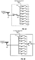
- FIGURES 5A and 5B illustrate a diversity receiver switch 508 configured to accommodate a lower power handling specification according to some aspects of the disclosure.
- the diversity receiver switch 508 is configured according to a lower power handling specification because of the different power handling specifications associated with on and off conditions of the diversity receiver switch 508.
- the diversity receiver switch 508 can be implemented in a diversity receiver path that also includes a diversity antenna 504 and a transceiver (not shown).
- the diversity receiver switch 508 includes a first stage including a switch SW-9 ( FIGURE 5A ) or a bank of first stage switches 510 ( FIGURE 5B ) and a second stage including the bank of second stage switches 520 ( FIGURE 5A ) or the switch SW-9 ( FIGURE 5B ).
- the first stage and the second stage can be interchanged (as in FIGURE 5B relative to FIGURE 5A ) depending on the desired applications.
- the two-stage configuration may operate according to the on and the off conditions of the diversity receiver switch 508.
- FIGURE 5A illustrates that when the diversity receiver switch is off, the first stage, which includes one switch SW-9 is specified to handle a higher power.
- conventional one stage configurations specify that all of the switches handle the higher power associated with the off condition.
- Each switch SW-1 to SW-8 of the bank of second stage switches 520 of FIGURE 5A is configured to communicate with the transceiver (not shown) based on the selected band associated with each switch SW-1 to SW-8.
- the switch SW-9 of FIGURE 5B is configured to communicate with the transceiver (not shown).
- the diversity antenna 504 may be coupled to the first stage, which includes the switch SW-9 ( FIGURE 5A ) or the bank of first stage switches 510 via an interconnect 502 ( FIGURE 5B ).
- FIGURES 5A and 5B illustrate that the interconnect 502 directly couples the switch SW-9 or the bank of first stage switches 510 to the diversity antenna 504, the diversity antenna 504 may be indirectly coupled to the first stage switch SW-9 or the bank of first stage switches 510.
- the switch SW-9 may be coupled to the bank of second stage switches 520 via an interconnect 506, as shown in FIGURE 5A .
- FIGURES 5A and 5B illustrate that the interconnect 506 directly couples the switch SW-9 to the bank of first/second stage switches 510/520, the bank of first/second stage switches 510/520 may be indirectly coupled to the switch SW-9.
- the switch SW-9 is implemented as a single pole single throw switch configuration.
- each switch SW-1 to SW-8 of the bank of second stage switches 520 is implemented as a single pole single throw switch configuration.
- the bank of first/second stage switches 510/520 may be implemented as a single pole multi-throw configuration.
- the diversity receiver switch 508 can be implemented to support the GSM mode when the diversity receiver switch 508 is in an off state. In this state, the power leaked from a primary antenna to the diversity antenna 504 is greater than the power handling capacity associated with the on state (e.g., in a WCDMA mode) of the diversity receiver switch 508. In the off state, the power handling capability of the diversity receiver switch 508 is based on the power leaked from the primary antenna to the diversity antenna 504.
- the power handling capability of the diversity receiver switch 508, in the off state is 26 dB, or a similar power level.
- the first stage switch SW-9 of the diversity receiver switch 508 is configured to accommodate the off state power level of the diversity receiver switch 508. For example, in operation the first stage switch SW-9 is set to an off position to absorb or accommodate the 26 dB power leaked from the primary antenna to the diversity receiver switch 508.
- the diversity receiver switch 508 also supports a WCDMA mode when the diversity receiver switch 508 is in an on state. In this state, the power specified for the diversity receiver switch 508 is less than when the diversity receiver switch 508 is in the off state. For example, during transmission on the primary transceiver path, the standard transmit power is set to about 23 dB and for some WCDMA implementations, 24 dB or a similar power level. Because there are no transmitters in the diversity receiver path, the primary antenna is isolated from the diversity antenna 504.
- a 10 dB (or similar power difference) isolation naturally exists (due to physical distance) between the primary antenna and the diversity antenna 504.
- the power handling capability at the diversity receiver switch 508 is specified by subtracting the 10 dB difference from the 23 dB or 24 dB standard transmit power, which results in a 13 dB or 14 dB power specification at the diversity receiver switch 508.
- an additional 3 dB of power is accounted for at the diversity receiver switch 508 to accommodate an impedance mismatch at the diversity receiver switch 508.
- the power handling specification of the diversity receiver switch 508 in the on state is about 17 dB, or a similar power level.
- the power handling capability of the diversity receiver switch 508 is much less than the power handling capability of a conventional diversity switch or a primary transceiver switch, the number of transistors specified for the current diversity receiver switch 508 is reduced. By reducing the number of transistors, the overall size of the diversity receiver switch 508 is also reduced. In general, every 3 dB reduction of the power handling specification can result in a reduction of the switch size by half. As a result, one configuration of the proposed two-stage design for a diversity receiver switch provides a significant size and cost reduction.
- the current diversity receiver switch 508 accommodates the on and off state by a two-stage design, instead of burdening every port of each switch with the off-state power handling.
- the two-stage switch design can be applied in any of the gallium arsenide (GaAs), Silicon on Insulator (SOI), Silicon on Sapphire (SOS), Silicon on Glass (SOG) and other CMOS technologies, for any application where a high power handling capability is specified in an off state, while a low power handling is specified in the on state.
- GaAs gallium arsenide
- SOI Silicon on Insulator
- SOS Silicon on Sapphire
- SOG Silicon on Glass
- the order of the first stage (or high power handling specification stage) and the second stage may be interchanged based on different applications.
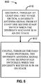
- FIGURE 6 is a flow diagram illustrating a method 600 for communication within a diversity receiver switch according to one aspect of the present disclosure.
- a diversity antenna signal is decoupled, through at least one first stage switch, from at least one second stage switch when the diversity receiver is in an off state, as shown at block 610.
- FIGURE 5A illustrates that when the diversity receiver switch is off, the first stage, which includes one switch SW-9 specified to handle a higher power.
- FIGURE 5B when the diversity receiver switch is off, the second stage, which includes the switch SW-9 is specified to handle a higher power than the first stage switches 510, which includes switches SW-1 to SW-8.
- the diversity antenna signal is coupled, through the first stage switch(es), to the second stage switch(es) when the diversity receiver is in an on state, as shown in block 612.
- FIGURES 5A illustrate that the interconnect 506 couples the switch SW-9 to the bank of second stage switches 520 during an on state.
- the first stage switch(es) is configured to handle a different amount of power than the second stage switch(es).
- the switch SW-9 is coupled to the bank of the first stage switches 510 via the interconnect 506 during the on state and is specified to handle a higher power than the first stage switches 510.
- the diversity receiver switch includes means for switching communications with a transceiver.
- the means for switching communications may be the bank of second stage switches 520, the diversity receiver switch 308 and/or diversity receiver switch 208 configured to perform the functions recited by the means for switching communications, for example, as shown in FIGURES 2 , 3 , and 5A .
- the means for switching communications may be the switch SW-9 configured to perform the functions recited by the means for switching communications, for example, as shown in FIGURE 5B .
- the diversity receiver switch includes a means for switching communications between a diversity receiver antenna and a transceiver switching means.
- the antenna switching means may be the switch SW-9 configured to perform the functions recited by the antenna switching means, as shown in FIGURE 5A .
- the antenna switching means may also include a bank of first stage switches 510 configured to perform the functions recited by the antenna switching means, for example, as shown in FIGURE 5B .
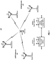
- FIGURE 7 is a block diagram showing an exemplary wireless communication system 700 in which an aspect of the disclosure may be advantageously employed.
- FIGURE 7 shows three remote units 720, 730, and 750 and two base stations 740. It will be recognized that wireless communication systems may have many more remote units and base stations/eNodeBs.
- Remote units 720, 730, and 750 include IC devices 725A, 725C and 725B, which include the disclosed diversity receiver switch.
- FIGURE 7 shows forward link signals 780 from the base station 740 to the remote units 720, 730, and 750 and reverse link signals 790 from the remote units 720, 730, and 750 to base stations 740.
- remote unit 720 is shown as a mobile telephone
- remote unit 730 is shown as a portable computer
- remote unit 750 is shown as a fixed location remote unit in a wireless local loop system.
- the remote units may be mobile phones, hand-held personal communication systems (PCS) units, portable data units such as personal data assistants, GPS enabled devices, navigation devices, set top boxes, music players, video players, entertainment units, fixed location data units such as meter reading equipment, or any other device that stores or retrieves data or computer instructions, or any combination thereof.
- FIGURE 7 illustrates remote units according to the teachings of the disclosure, the disclosure is not limited to these exemplary illustrated units. Aspects of the disclosure may be suitably employed in any device, which includes the diversity receiver switch.
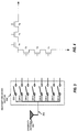
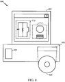
- FIGURE 8 is a block diagram illustrating a design workstation used for circuit, layout, and logic design of a semiconductor component, such as the diversity receiver switch disclosed above.
- a design workstation 800 includes a hard disk 801 containing operating system software, support files, and design software such as Cadence or OrCAD.
- the design workstation 800 also includes a display 802 to facilitate design of a circuit 810 or a semiconductor component 812 such as a diversity receiver switch.
- a storage medium 804 is provided for tangibly storing the circuit design 810 or the semiconductor component 812.
- the circuit design 810 or the semiconductor component 812 may be stored on the storage medium 804 in a file format such as GDSII or GERBER.
- the storage medium 804 may be a CD-ROM, DVD, hard disk, flash memory, or other appropriate device.
- the design workstation 800 includes a drive apparatus 803 for accepting input from or writing output to the storage medium 804.
- Data recorded on the storage medium 804 may specify logic circuit configurations, pattern data for photolithography masks, or mask pattern data for serial write tools such as electron beam lithography.
- the data may further include logic verification data such as timing diagrams or net circuits associated with logic simulations.
- Providing data on the storage medium 804 facilitates the design of the circuit design 810 or the semiconductor component 812 by decreasing the number of processes for designing semiconductor wafers.
- the methodologies described herein may be implemented by various means depending upon the application. For example, these methodologies may be implemented in hardware, firmware, software, or any combination thereof.
- the processing units may be implemented within one or more application specific integrated circuits (ASICs), digital signal processors (DSPs), digital signal processing devices (DSPDs), programmable logic devices (PLDs), field programmable gate arrays (FPGAs), processors, controllers, micro-controllers, microprocessors, electronic devices, other electronic units designed to perform the functions described herein, or a combination thereof.
- ASICs application specific integrated circuits
- DSPs digital signal processors
- DSPDs digital signal processing devices
- PLDs programmable logic devices
- FPGAs field programmable gate arrays
- processors controllers, micro-controllers, microprocessors, electronic devices, other electronic units designed to perform the functions described herein, or a combination thereof.
- the methodologies may be implemented with modules (e.g., procedures, functions, and so on) that perform the functions described herein.
- Any machine or computer readable medium tangibly embodying instructions may be used in implementing the methodologies described herein.
- software code may be stored in a memory and executed by a processor. When executed by the processor, the executing software code generates the operational environment that implements the various methodologies and functionalities of the different aspects of the teachings presented herein.
- Memory may be implemented within the processor or external to the processor.
- the term "memory" refers to any type of long term, short term, volatile, nonvolatile, or other memory and is not to be limited to any particular type of memory or number of memories, or type of media upon which memory is stored.
- the machine or computer readable medium that stores the software code defining the methodologies and functions described herein includes physical computer storage media.
- a storage medium may be any available medium that can be accessed by a computer.
- such computer-readable media can comprise RAM, ROM, EEPROM, CD-ROM or other optical disk storage, magnetic disk storage or other magnetic storage devices, or any other medium that can be used to store desired program code in the form of instructions or data structures and that can be accessed by a computer.
- disk and/or disc includes compact disc (CD), laser disc, optical disc, digital versatile disc (DVD), floppy disk and blu-ray disc where disks usually reproduce data magnetically, while discs reproduce data optically with lasers. Combinations of the above should also be included within the scope of computer readable media.
- instructions and/or data may be provided as signals on transmission media included in a communication apparatus.
- a communication apparatus may include a transceiver having signals indicative of instructions and data. The instructions and data are configured to cause one or more processors to implement the functions outlined in the claims.
Landscapes
- Engineering & Computer Science (AREA)
- Computer Networks & Wireless Communication (AREA)
- Signal Processing (AREA)
- Radio Transmission System (AREA)
- Circuits Of Receivers In General (AREA)
- Transceivers (AREA)
Applications Claiming Priority (2)
| Application Number | Priority Date | Filing Date | Title |
|---|---|---|---|
| US13/464,092 US9008602B2 (en) | 2012-05-04 | 2012-05-04 | Radio frequency switch for diversity receiver |
| PCT/US2013/039681 WO2013166486A1 (en) | 2012-05-04 | 2013-05-06 | Radio frequency switch for diversity receiver |
Publications (2)
| Publication Number | Publication Date |
|---|---|
| EP2845320A1 EP2845320A1 (en) | 2015-03-11 |
| EP2845320B1 true EP2845320B1 (en) | 2016-06-01 |
Family
ID=48471102
Family Applications (1)
| Application Number | Title | Priority Date | Filing Date |
|---|---|---|---|
| EP13724454.7A Active EP2845320B1 (en) | 2012-05-04 | 2013-05-06 | Radio frequency switch for diversity receiver |
Country Status (6)
| Country | Link |
|---|---|
| US (2) | US9008602B2 (enExample) |
| EP (1) | EP2845320B1 (enExample) |
| JP (1) | JP6037414B2 (enExample) |
| KR (1) | KR101668722B1 (enExample) |
| CN (1) | CN104272597B (enExample) |
| WO (1) | WO2013166486A1 (enExample) |
Families Citing this family (10)
| Publication number | Priority date | Publication date | Assignee | Title |
|---|---|---|---|---|
| US9008602B2 (en) | 2012-05-04 | 2015-04-14 | Qualcomm Incorporated | Radio frequency switch for diversity receiver |
| US9024838B2 (en) * | 2012-08-09 | 2015-05-05 | Qualcomm Incorporated | Multi-throw antenna switch with off-state capacitance reduction |
| US10361585B2 (en) | 2014-01-27 | 2019-07-23 | Ivani, LLC | Systems and methods to allow for a smart device |
| US10211004B2 (en) * | 2014-11-04 | 2019-02-19 | Ivani, LLC | Intelligent electrical switch |
| US9843291B2 (en) | 2015-08-07 | 2017-12-12 | Qualcomm Incorporated | Cascaded switch between pluralities of LNAS |
| TWI729112B (zh) * | 2016-04-09 | 2021-06-01 | 美商天工方案公司 | 具有可切換雙工器的前端架構 |
| WO2017210263A1 (en) * | 2016-06-01 | 2017-12-07 | Applied Materials, Inc. | High pressure ammonia nitridation of tunnel oxide for 3dnand applications |
| US10250251B1 (en) * | 2018-02-07 | 2019-04-02 | Infineon Technologies Ag | RF sensor in stacked transistors |
| US10608604B2 (en) * | 2018-07-09 | 2020-03-31 | Mediatek Inc. | Wireless communications circuit and associated wireless communications device with reduced power loss and reduced circuit area |
| CN109768811A (zh) * | 2019-02-12 | 2019-05-17 | 努比亚技术有限公司 | 双天线间辐射杂散的控制方法、通信终端及计算机可读存储介质 |
Family Cites Families (28)
| Publication number | Priority date | Publication date | Assignee | Title |
|---|---|---|---|---|
| JP3434732B2 (ja) * | 1999-06-17 | 2003-08-11 | 埼玉日本電気株式会社 | アンテナ切替装置 |
| US6965788B1 (en) * | 2001-09-28 | 2005-11-15 | Arraycomm, Inc. | Method and apparatus for providing spatial processing in a remote unit |
| US7796969B2 (en) * | 2001-10-10 | 2010-09-14 | Peregrine Semiconductor Corporation | Symmetrically and asymmetrically stacked transistor group RF switch |
| US6804502B2 (en) | 2001-10-10 | 2004-10-12 | Peregrine Semiconductor Corporation | Switch circuit and method of switching radio frequency signals |
| US20040038660A1 (en) * | 2002-08-21 | 2004-02-26 | Ziming He | RF front-end for dual-mode wireless LAN module |
| US7929985B2 (en) * | 2003-05-01 | 2011-04-19 | Telefonaktiebolaget Lm Ericsson (Publ) | Multiple antenna receiver |
| US7317903B2 (en) * | 2003-09-30 | 2008-01-08 | Sharp Kabushiki Kaisha | Wireless communication circuit, wireless communication apparatus, and wireless communication system |
| KR100592767B1 (ko) * | 2003-12-26 | 2006-06-26 | 한국전자통신연구원 | 개선된 전력증폭기 효율을 가진 듀얼 안테나 다이버시티송신기 및 시스템 |
| US7505790B2 (en) | 2005-06-07 | 2009-03-17 | Integrated Systems Solution Corp. | Antenna diversity switch of wireless dual-mode co-existence systems |
| JP4696985B2 (ja) * | 2006-03-17 | 2011-06-08 | 株式会社村田製作所 | 無線通信装置 |
| US8254865B2 (en) * | 2006-04-07 | 2012-08-28 | Belair Networks | System and method for frequency offsetting of information communicated in MIMO-based wireless networks |
| US7772648B1 (en) | 2006-09-13 | 2010-08-10 | Rf Micro Devices, Inc. | Performance enhanced silicon-on-insulator technology |
| US20100197263A1 (en) * | 2009-01-30 | 2010-08-05 | Research In Motion Limited | Method and apparatus for combined multi-carrier reception and receive antenna diversity |
| US8457685B1 (en) * | 2009-04-20 | 2013-06-04 | Rf Micro Devices, Inc. | Method and system for increasing efficiency in a radio front-end |
| US8451044B2 (en) | 2009-06-29 | 2013-05-28 | Sige Semiconductor, Inc. | Switching circuit |
| WO2011045442A2 (en) | 2009-10-16 | 2011-04-21 | Ferfics Limited | Switching system and method |
| WO2011094284A1 (en) | 2010-01-26 | 2011-08-04 | Maxlinear, Inc. | Diversity receiver |
| WO2011119659A1 (en) * | 2010-03-23 | 2011-09-29 | Rf Micro Devices, Inc. | Adaptive antenna neutralization network |
| US8552816B2 (en) * | 2010-03-23 | 2013-10-08 | Rf Micro Devices, Inc. | Multiband simultaneous transmission and reception front end architecture |
| TW201138312A (en) | 2010-04-30 | 2011-11-01 | Ind Tech Res Inst | Comparison apparatus and speed-up method for comparator |
| US8390395B2 (en) | 2010-05-03 | 2013-03-05 | Raytheon Company | High power RF switch with active device size tapering |
| JP5697024B2 (ja) | 2010-12-22 | 2015-04-08 | サンデン株式会社 | 圧縮機 |
| US8838057B2 (en) * | 2011-04-04 | 2014-09-16 | Maxlinear, Inc. | Harmonic rejection mixer architecture with reduced sensitivity to gain and phase mismatches |
| US9763185B2 (en) * | 2012-02-13 | 2017-09-12 | Apple Inc. | Methods and apparatus for intelligent receiver operation |
| WO2013155494A1 (en) * | 2012-04-12 | 2013-10-17 | Skyworks Solutions, Inc. | Systems and methods related to improved isolation between transmit and receive radio-frequency signals |
| KR101915526B1 (ko) * | 2012-04-17 | 2018-11-06 | 삼성전자 주식회사 | 휴대 단말기의 안테나 장치 |
| US8868011B2 (en) * | 2012-04-30 | 2014-10-21 | Triquint Semiconductor, Inc. | Power amplifier with fast loadline modulation |
| US9008602B2 (en) | 2012-05-04 | 2015-04-14 | Qualcomm Incorporated | Radio frequency switch for diversity receiver |
-
2012
- 2012-05-04 US US13/464,092 patent/US9008602B2/en active Active
-
2013
- 2013-05-06 JP JP2015510503A patent/JP6037414B2/ja active Active
- 2013-05-06 KR KR1020147033923A patent/KR101668722B1/ko active Active
- 2013-05-06 CN CN201380023057.7A patent/CN104272597B/zh active Active
- 2013-05-06 WO PCT/US2013/039681 patent/WO2013166486A1/en not_active Ceased
- 2013-05-06 EP EP13724454.7A patent/EP2845320B1/en active Active
-
2015
- 2015-04-10 US US14/684,072 patent/US9379802B2/en active Active
Also Published As
| Publication number | Publication date |
|---|---|
| WO2013166486A1 (en) | 2013-11-07 |
| US20130295866A1 (en) | 2013-11-07 |
| EP2845320A1 (en) | 2015-03-11 |
| US9379802B2 (en) | 2016-06-28 |
| CN104272597A (zh) | 2015-01-07 |
| CN104272597B (zh) | 2017-11-07 |
| JP2015517753A (ja) | 2015-06-22 |
| US9008602B2 (en) | 2015-04-14 |
| US20150215026A1 (en) | 2015-07-30 |
| KR101668722B1 (ko) | 2016-10-24 |
| KR20150006875A (ko) | 2015-01-19 |
| JP6037414B2 (ja) | 2016-12-07 |
Similar Documents
| Publication | Publication Date | Title |
|---|---|---|
| EP2845320B1 (en) | Radio frequency switch for diversity receiver | |
| US9660691B2 (en) | Antenna interface circuits with quadplexers | |
| KR102403105B1 (ko) | 간헐적 방출들 및/또는 공존 사양들에 대한 프론트 엔드 아키텍처 | |
| US10910714B2 (en) | Configurable power combiner and splitter | |
| KR102160715B1 (ko) | 캐리어 어그리게이션을 위해 캐스코드 디버트 스위치를 갖는 저 잡음 증폭기 | |
| CN107925423B (zh) | 多个lna之间的级联开关 | |
| US20140072001A1 (en) | Carrier aggregation receiver architecture | |
| CN113364478B (zh) | 优化功率钳位的方法和装置 | |
| CN103380573A (zh) | 具有嵌入式阻抗变换的前端rf滤波器 | |
| US9419674B2 (en) | Shared filter for transmit and receive paths | |
| US10985461B2 (en) | Terminal device | |
| TWI664810B (zh) | 與多模多頻段功率放大器之低功率效能改進有關之系統、電路及方法 | |
| JP2018182720A (ja) | 電力増幅モジュール及び高周波モジュール | |
| WO2018031198A1 (en) | Multi-stage bandpass low-noise amplifier | |
| JPWO2011004525A1 (ja) | マルチバンド無線機 | |
| US20150180465A1 (en) | Rf switch | |
| EP2693644A1 (en) | Mobile wireless communications device with lna front end circuit and related methods | |
| US20250096751A1 (en) | Darlington Circuit with a Driver Amplifier | |
| US12445125B2 (en) | Switching circuit | |
| US20250096741A1 (en) | Interstage Darlington Circuit |
Legal Events
| Date | Code | Title | Description |
|---|---|---|---|
| PUAI | Public reference made under article 153(3) epc to a published international application that has entered the european phase |
Free format text: ORIGINAL CODE: 0009012 |
|
| 17P | Request for examination filed |
Effective date: 20141003 |
|
| AK | Designated contracting states |
Kind code of ref document: A1 Designated state(s): AL AT BE BG CH CY CZ DE DK EE ES FI FR GB GR HR HU IE IS IT LI LT LU LV MC MK MT NL NO PL PT RO RS SE SI SK SM TR |
|
| AX | Request for extension of the european patent |
Extension state: BA ME |
|
| DAX | Request for extension of the european patent (deleted) | ||
| GRAP | Despatch of communication of intention to grant a patent |
Free format text: ORIGINAL CODE: EPIDOSNIGR1 |
|
| INTG | Intention to grant announced |
Effective date: 20151222 |
|
| GRAS | Grant fee paid |
Free format text: ORIGINAL CODE: EPIDOSNIGR3 |
|
| GRAA | (expected) grant |
Free format text: ORIGINAL CODE: 0009210 |
|
| AK | Designated contracting states |
Kind code of ref document: B1 Designated state(s): AL AT BE BG CH CY CZ DE DK EE ES FI FR GB GR HR HU IE IS IT LI LT LU LV MC MK MT NL NO PL PT RO RS SE SI SK SM TR |
|
| REG | Reference to a national code |
Ref country code: GB Ref legal event code: FG4D |
|
| REG | Reference to a national code |
Ref country code: CH Ref legal event code: EP Ref country code: AT Ref legal event code: REF Ref document number: 804423 Country of ref document: AT Kind code of ref document: T Effective date: 20160615 |
|
| REG | Reference to a national code |
Ref country code: IE Ref legal event code: FG4D |
|
| REG | Reference to a national code |
Ref country code: DE Ref legal event code: R096 Ref document number: 602013008236 Country of ref document: DE |
|
| REG | Reference to a national code |
Ref country code: LT Ref legal event code: MG4D |
|
| REG | Reference to a national code |
Ref country code: NL Ref legal event code: MP Effective date: 20160601 |
|
| PG25 | Lapsed in a contracting state [announced via postgrant information from national office to epo] |
Ref country code: LT Free format text: LAPSE BECAUSE OF FAILURE TO SUBMIT A TRANSLATION OF THE DESCRIPTION OR TO PAY THE FEE WITHIN THE PRESCRIBED TIME-LIMIT Effective date: 20160601 Ref country code: NO Free format text: LAPSE BECAUSE OF FAILURE TO SUBMIT A TRANSLATION OF THE DESCRIPTION OR TO PAY THE FEE WITHIN THE PRESCRIBED TIME-LIMIT Effective date: 20160901 Ref country code: FI Free format text: LAPSE BECAUSE OF FAILURE TO SUBMIT A TRANSLATION OF THE DESCRIPTION OR TO PAY THE FEE WITHIN THE PRESCRIBED TIME-LIMIT Effective date: 20160601 |
|
| REG | Reference to a national code |
Ref country code: AT Ref legal event code: MK05 Ref document number: 804423 Country of ref document: AT Kind code of ref document: T Effective date: 20160601 |
|
| PG25 | Lapsed in a contracting state [announced via postgrant information from national office to epo] |
Ref country code: RS Free format text: LAPSE BECAUSE OF FAILURE TO SUBMIT A TRANSLATION OF THE DESCRIPTION OR TO PAY THE FEE WITHIN THE PRESCRIBED TIME-LIMIT Effective date: 20160601 Ref country code: GR Free format text: LAPSE BECAUSE OF FAILURE TO SUBMIT A TRANSLATION OF THE DESCRIPTION OR TO PAY THE FEE WITHIN THE PRESCRIBED TIME-LIMIT Effective date: 20160902 Ref country code: LV Free format text: LAPSE BECAUSE OF FAILURE TO SUBMIT A TRANSLATION OF THE DESCRIPTION OR TO PAY THE FEE WITHIN THE PRESCRIBED TIME-LIMIT Effective date: 20160601 Ref country code: HR Free format text: LAPSE BECAUSE OF FAILURE TO SUBMIT A TRANSLATION OF THE DESCRIPTION OR TO PAY THE FEE WITHIN THE PRESCRIBED TIME-LIMIT Effective date: 20160601 Ref country code: SE Free format text: LAPSE BECAUSE OF FAILURE TO SUBMIT A TRANSLATION OF THE DESCRIPTION OR TO PAY THE FEE WITHIN THE PRESCRIBED TIME-LIMIT Effective date: 20160601 Ref country code: ES Free format text: LAPSE BECAUSE OF FAILURE TO SUBMIT A TRANSLATION OF THE DESCRIPTION OR TO PAY THE FEE WITHIN THE PRESCRIBED TIME-LIMIT Effective date: 20160601 Ref country code: NL Free format text: LAPSE BECAUSE OF FAILURE TO SUBMIT A TRANSLATION OF THE DESCRIPTION OR TO PAY THE FEE WITHIN THE PRESCRIBED TIME-LIMIT Effective date: 20160601 |
|
| PG25 | Lapsed in a contracting state [announced via postgrant information from national office to epo] |
Ref country code: SK Free format text: LAPSE BECAUSE OF FAILURE TO SUBMIT A TRANSLATION OF THE DESCRIPTION OR TO PAY THE FEE WITHIN THE PRESCRIBED TIME-LIMIT Effective date: 20160601 Ref country code: IS Free format text: LAPSE BECAUSE OF FAILURE TO SUBMIT A TRANSLATION OF THE DESCRIPTION OR TO PAY THE FEE WITHIN THE PRESCRIBED TIME-LIMIT Effective date: 20161001 Ref country code: RO Free format text: LAPSE BECAUSE OF FAILURE TO SUBMIT A TRANSLATION OF THE DESCRIPTION OR TO PAY THE FEE WITHIN THE PRESCRIBED TIME-LIMIT Effective date: 20160601 Ref country code: IT Free format text: LAPSE BECAUSE OF FAILURE TO SUBMIT A TRANSLATION OF THE DESCRIPTION OR TO PAY THE FEE WITHIN THE PRESCRIBED TIME-LIMIT Effective date: 20160601 Ref country code: EE Free format text: LAPSE BECAUSE OF FAILURE TO SUBMIT A TRANSLATION OF THE DESCRIPTION OR TO PAY THE FEE WITHIN THE PRESCRIBED TIME-LIMIT Effective date: 20160601 Ref country code: CZ Free format text: LAPSE BECAUSE OF FAILURE TO SUBMIT A TRANSLATION OF THE DESCRIPTION OR TO PAY THE FEE WITHIN THE PRESCRIBED TIME-LIMIT Effective date: 20160601 |
|
| PG25 | Lapsed in a contracting state [announced via postgrant information from national office to epo] |
Ref country code: PT Free format text: LAPSE BECAUSE OF FAILURE TO SUBMIT A TRANSLATION OF THE DESCRIPTION OR TO PAY THE FEE WITHIN THE PRESCRIBED TIME-LIMIT Effective date: 20161003 Ref country code: SM Free format text: LAPSE BECAUSE OF FAILURE TO SUBMIT A TRANSLATION OF THE DESCRIPTION OR TO PAY THE FEE WITHIN THE PRESCRIBED TIME-LIMIT Effective date: 20160601 Ref country code: AT Free format text: LAPSE BECAUSE OF FAILURE TO SUBMIT A TRANSLATION OF THE DESCRIPTION OR TO PAY THE FEE WITHIN THE PRESCRIBED TIME-LIMIT Effective date: 20160601 Ref country code: PL Free format text: LAPSE BECAUSE OF FAILURE TO SUBMIT A TRANSLATION OF THE DESCRIPTION OR TO PAY THE FEE WITHIN THE PRESCRIBED TIME-LIMIT Effective date: 20160601 Ref country code: BE Free format text: LAPSE BECAUSE OF FAILURE TO SUBMIT A TRANSLATION OF THE DESCRIPTION OR TO PAY THE FEE WITHIN THE PRESCRIBED TIME-LIMIT Effective date: 20160601 |
|
| REG | Reference to a national code |
Ref country code: DE Ref legal event code: R097 Ref document number: 602013008236 Country of ref document: DE |
|
| PLBE | No opposition filed within time limit |
Free format text: ORIGINAL CODE: 0009261 |
|
| STAA | Information on the status of an ep patent application or granted ep patent |
Free format text: STATUS: NO OPPOSITION FILED WITHIN TIME LIMIT |
|
| REG | Reference to a national code |
Ref country code: FR Ref legal event code: PLFP Year of fee payment: 5 |
|
| 26N | No opposition filed |
Effective date: 20170302 |
|
| PG25 | Lapsed in a contracting state [announced via postgrant information from national office to epo] |
Ref country code: SI Free format text: LAPSE BECAUSE OF FAILURE TO SUBMIT A TRANSLATION OF THE DESCRIPTION OR TO PAY THE FEE WITHIN THE PRESCRIBED TIME-LIMIT Effective date: 20160601 Ref country code: DK Free format text: LAPSE BECAUSE OF FAILURE TO SUBMIT A TRANSLATION OF THE DESCRIPTION OR TO PAY THE FEE WITHIN THE PRESCRIBED TIME-LIMIT Effective date: 20160601 |
|
| PG25 | Lapsed in a contracting state [announced via postgrant information from national office to epo] |
Ref country code: LU Free format text: LAPSE BECAUSE OF NON-PAYMENT OF DUE FEES Effective date: 20170531 |
|
| REG | Reference to a national code |
Ref country code: CH Ref legal event code: PL |
|
| PG25 | Lapsed in a contracting state [announced via postgrant information from national office to epo] |
Ref country code: MC Free format text: LAPSE BECAUSE OF FAILURE TO SUBMIT A TRANSLATION OF THE DESCRIPTION OR TO PAY THE FEE WITHIN THE PRESCRIBED TIME-LIMIT Effective date: 20160601 |
|
| REG | Reference to a national code |
Ref country code: IE Ref legal event code: MM4A |
|
| PG25 | Lapsed in a contracting state [announced via postgrant information from national office to epo] |
Ref country code: CH Free format text: LAPSE BECAUSE OF NON-PAYMENT OF DUE FEES Effective date: 20170531 Ref country code: LI Free format text: LAPSE BECAUSE OF NON-PAYMENT OF DUE FEES Effective date: 20170531 |
|
| PG25 | Lapsed in a contracting state [announced via postgrant information from national office to epo] |
Ref country code: LU Free format text: LAPSE BECAUSE OF NON-PAYMENT OF DUE FEES Effective date: 20170506 |
|
| REG | Reference to a national code |
Ref country code: FR Ref legal event code: PLFP Year of fee payment: 6 |
|
| PG25 | Lapsed in a contracting state [announced via postgrant information from national office to epo] |
Ref country code: IE Free format text: LAPSE BECAUSE OF NON-PAYMENT OF DUE FEES Effective date: 20170506 |
|
| PG25 | Lapsed in a contracting state [announced via postgrant information from national office to epo] |
Ref country code: MT Free format text: LAPSE BECAUSE OF NON-PAYMENT OF DUE FEES Effective date: 20170506 |
|
| PG25 | Lapsed in a contracting state [announced via postgrant information from national office to epo] |
Ref country code: AL Free format text: LAPSE BECAUSE OF FAILURE TO SUBMIT A TRANSLATION OF THE DESCRIPTION OR TO PAY THE FEE WITHIN THE PRESCRIBED TIME-LIMIT Effective date: 20160601 |
|
| PG25 | Lapsed in a contracting state [announced via postgrant information from national office to epo] |
Ref country code: HU Free format text: LAPSE BECAUSE OF FAILURE TO SUBMIT A TRANSLATION OF THE DESCRIPTION OR TO PAY THE FEE WITHIN THE PRESCRIBED TIME-LIMIT; INVALID AB INITIO Effective date: 20130506 |
|
| PG25 | Lapsed in a contracting state [announced via postgrant information from national office to epo] |
Ref country code: BG Free format text: LAPSE BECAUSE OF FAILURE TO SUBMIT A TRANSLATION OF THE DESCRIPTION OR TO PAY THE FEE WITHIN THE PRESCRIBED TIME-LIMIT Effective date: 20160601 |
|
| PG25 | Lapsed in a contracting state [announced via postgrant information from national office to epo] |
Ref country code: CY Free format text: LAPSE BECAUSE OF FAILURE TO SUBMIT A TRANSLATION OF THE DESCRIPTION OR TO PAY THE FEE WITHIN THE PRESCRIBED TIME-LIMIT Effective date: 20160601 |
|
| PG25 | Lapsed in a contracting state [announced via postgrant information from national office to epo] |
Ref country code: MK Free format text: LAPSE BECAUSE OF FAILURE TO SUBMIT A TRANSLATION OF THE DESCRIPTION OR TO PAY THE FEE WITHIN THE PRESCRIBED TIME-LIMIT Effective date: 20160601 |
|
| PG25 | Lapsed in a contracting state [announced via postgrant information from national office to epo] |
Ref country code: TR Free format text: LAPSE BECAUSE OF FAILURE TO SUBMIT A TRANSLATION OF THE DESCRIPTION OR TO PAY THE FEE WITHIN THE PRESCRIBED TIME-LIMIT Effective date: 20160601 |
|
| REG | Reference to a national code |
Ref country code: DE Ref legal event code: R082 Ref document number: 602013008236 Country of ref document: DE Representative=s name: MAUCHER JENKINS PATENTANWAELTE & RECHTSANWAELT, DE |
|
| REG | Reference to a national code |
Ref country code: FR Ref legal event code: PLFP Year of fee payment: 11 |
|
| PGFP | Annual fee paid to national office [announced via postgrant information from national office to epo] |
Ref country code: DE Payment date: 20250409 Year of fee payment: 13 |
|
| PGFP | Annual fee paid to national office [announced via postgrant information from national office to epo] |
Ref country code: GB Payment date: 20250410 Year of fee payment: 13 |
|
| PGFP | Annual fee paid to national office [announced via postgrant information from national office to epo] |
Ref country code: FR Payment date: 20250409 Year of fee payment: 13 |