EP2845234B1 - Verfahren zum beschichten einer leiterplatte eines led-moduls - Google Patents
Verfahren zum beschichten einer leiterplatte eines led-moduls Download PDFInfo
- Publication number
- EP2845234B1 EP2845234B1 EP13712700.7A EP13712700A EP2845234B1 EP 2845234 B1 EP2845234 B1 EP 2845234B1 EP 13712700 A EP13712700 A EP 13712700A EP 2845234 B1 EP2845234 B1 EP 2845234B1
- Authority
- EP
- European Patent Office
- Prior art keywords
- circuit board
- printed circuit
- led module
- highly reflective
- led
- Prior art date
- Legal status (The legal status is an assumption and is not a legal conclusion. Google has not performed a legal analysis and makes no representation as to the accuracy of the status listed.)
- Not-in-force
Links
Images


Classifications
-
- H—ELECTRICITY
- H10—SEMICONDUCTOR DEVICES; ELECTRIC SOLID-STATE DEVICES NOT OTHERWISE PROVIDED FOR
- H10H—INORGANIC LIGHT-EMITTING SEMICONDUCTOR DEVICES HAVING POTENTIAL BARRIERS
- H10H20/00—Individual inorganic light-emitting semiconductor devices having potential barriers, e.g. light-emitting diodes [LED]
- H10H20/80—Constructional details
- H10H20/84—Coatings, e.g. passivation layers or antireflective coatings
- H10H20/841—Reflective coatings, e.g. dielectric Bragg reflectors
-
- H—ELECTRICITY
- H10—SEMICONDUCTOR DEVICES; ELECTRIC SOLID-STATE DEVICES NOT OTHERWISE PROVIDED FOR
- H10H—INORGANIC LIGHT-EMITTING SEMICONDUCTOR DEVICES HAVING POTENTIAL BARRIERS
- H10H20/00—Individual inorganic light-emitting semiconductor devices having potential barriers, e.g. light-emitting diodes [LED]
- H10H20/80—Constructional details
- H10H20/85—Packages
- H10H20/855—Optical field-shaping means, e.g. lenses
- H10H20/856—Reflecting means
-
- H—ELECTRICITY
- H05—ELECTRIC TECHNIQUES NOT OTHERWISE PROVIDED FOR
- H05K—PRINTED CIRCUITS; CASINGS OR CONSTRUCTIONAL DETAILS OF ELECTRIC APPARATUS; MANUFACTURE OF ASSEMBLAGES OF ELECTRICAL COMPONENTS
- H05K1/00—Printed circuits
- H05K1/02—Details
- H05K1/0201—Thermal arrangements, e.g. for cooling, heating or preventing overheating
- H05K1/0203—Cooling of mounted components
- H05K1/021—Components thermally connected to metal substrates or heat-sinks by insert mounting
-
- H—ELECTRICITY
- H05—ELECTRIC TECHNIQUES NOT OTHERWISE PROVIDED FOR
- H05K—PRINTED CIRCUITS; CASINGS OR CONSTRUCTIONAL DETAILS OF ELECTRIC APPARATUS; MANUFACTURE OF ASSEMBLAGES OF ELECTRICAL COMPONENTS
- H05K2201/00—Indexing scheme relating to printed circuits covered by H05K1/00
- H05K2201/09—Shape and layout
- H05K2201/09818—Shape or layout details not covered by a single group of H05K2201/09009 - H05K2201/09809
- H05K2201/09827—Tapered, e.g. tapered hole, via or groove
-
- H—ELECTRICITY
- H05—ELECTRIC TECHNIQUES NOT OTHERWISE PROVIDED FOR
- H05K—PRINTED CIRCUITS; CASINGS OR CONSTRUCTIONAL DETAILS OF ELECTRIC APPARATUS; MANUFACTURE OF ASSEMBLAGES OF ELECTRICAL COMPONENTS
- H05K2201/00—Indexing scheme relating to printed circuits covered by H05K1/00
- H05K2201/10—Details of components or other objects attached to or integrated in a printed circuit board
- H05K2201/10007—Types of components
- H05K2201/10106—Light emitting diode [LED]
-
- H—ELECTRICITY
- H05—ELECTRIC TECHNIQUES NOT OTHERWISE PROVIDED FOR
- H05K—PRINTED CIRCUITS; CASINGS OR CONSTRUCTIONAL DETAILS OF ELECTRIC APPARATUS; MANUFACTURE OF ASSEMBLAGES OF ELECTRICAL COMPONENTS
- H05K2201/00—Indexing scheme relating to printed circuits covered by H05K1/00
- H05K2201/20—Details of printed circuits not provided for in H05K2201/01 - H05K2201/10
- H05K2201/2054—Light-reflecting surface, e.g. conductors, substrates, coatings, dielectrics
-
- H—ELECTRICITY
- H10—SEMICONDUCTOR DEVICES; ELECTRIC SOLID-STATE DEVICES NOT OTHERWISE PROVIDED FOR
- H10H—INORGANIC LIGHT-EMITTING SEMICONDUCTOR DEVICES HAVING POTENTIAL BARRIERS
- H10H20/00—Individual inorganic light-emitting semiconductor devices having potential barriers, e.g. light-emitting diodes [LED]
- H10H20/01—Manufacture or treatment
- H10H20/034—Manufacture or treatment of coatings
-
- H—ELECTRICITY
- H10—SEMICONDUCTOR DEVICES; ELECTRIC SOLID-STATE DEVICES NOT OTHERWISE PROVIDED FOR
- H10H—INORGANIC LIGHT-EMITTING SEMICONDUCTOR DEVICES HAVING POTENTIAL BARRIERS
- H10H20/00—Individual inorganic light-emitting semiconductor devices having potential barriers, e.g. light-emitting diodes [LED]
- H10H20/01—Manufacture or treatment
- H10H20/036—Manufacture or treatment of packages
- H10H20/0363—Manufacture or treatment of packages of optical field-shaping means
Definitions
- the present invention comprises an LED module comprising a coated circuit board and the coated circuit board itself.
- the coated circuit board serves to supply a portion of the light emitted laterally from an LED chip of the LED module in the direction of the normal axis of the LED module judge.
- a method for coating a printed circuit board of an LED module is presented.
- a circuit board with a recess in an LED module to reflect light emitted from an LED chip of the LED module to the outside and to specify a direction of radiation.
- a printed circuit board is made of a plastic whose surface is covered with a copper sheet.
- the copper track is capable of reflecting light, but the efficiency is low.
- the LED chip is placed in the LED module in the recess of the circuit board so that it emits light from behind through the recess out of the LED module out.
- the US 2011/0198628 A1 a multichip light emitting diode (LED) package comprising a printed circuit board (PCB) having a tapered via hole and a circuit interconnect line on a surface of the PCB.
- the US 2003/0193055 A1 refers to a lighting device with a light emitting diode (LED).
- the device includes a metal substrate having a surface.
- a dielectric coating layer is superimposed on the surface of the metal substrate.
- a light emitting diode (LED) is on the dielectric coating layer positioned.
- the metal substrate serves as a heat sink for the heat emitted by the LED during operation.
- the WO 2012/002580 A1 and the US 2013/0099276 A1 refer to an LED light source device comprising: a substrate, an electrode formed on the substrate, a white inorganic resist layer deposited over the substrate to cover a surface thereof except where the electrode is formed, and a LED element connected to the electrode, wherein the white inorganic resist layer contains fine white inorganic particles dispersed or mixed in an inorganic binder.
- the EP 1 978 566 A1 relates to a light source device comprising: a substrate comprising at least a pair of electrodes, at least one light emitting device and a transparent resin for sealing the light emitting device, wherein a white resist layer is formed on the substrate.
- the US 2004/222433 A1 refers to an LED module with a metallic carrier which is covered with a thick ceramic layer. On the surface of this ceramic layer, in the recess of which a light-emitting diode is arranged, a reflective layer can be sprayed on.
- the present invention therefore proposes as a basic idea to provide a surface of a printed circuit board with a highly reflective layer.
- conventional coating processes such as screen printing or curtain coating, are not well suited for this because they do not achieve a satisfactory uniform coating, in particular of the boundary walls of a recesses of the printed circuit board.
- screenprints can initially be used for coarser structures, they are unsuitable for finer structures.
- the present invention has as its object to improve all the disadvantages of the prior art mentioned.
- it is an object of the present invention to increase the luminous efficacy of an LED module and to provide an improved method for coating a printed circuit board.
- a printed circuit board with improved reflection properties for an LED module is to be produced in particular.
- the invention aims to avoid the disadvantages of common processes and methods.
- the boundary walls of recesses in a circuit board to be provided with good reflection properties.
- the present invention achieves the above-mentioned objects according to the subject-matter of independent claim 1.
- the dependent claims further develop the gist of the invention in an advantageous manner.
- Fig. 1 shows an LED module 10 according to an example, which is not part of the invention, as well as a circuit board 1.
- the circuit board 1 is part of the LED module 10, but also individually from the example comprises.
- the LED module 10 consists of at least one LED chip 6, which is applied to a carrier plate 5.
- the at least one LED chip 6 may be, for example, a conventional LED, an OLED, an array of multiple LEDs or an LED track. Several LEDs can emit either the same or different colored light.
- the carrier plate 5 optionally have suitable receiving means for the at least one LED chip 6.
- the carrier plate can be constructed in multiple layers.
- the carrier plate 5 may contain materials containing, for example, aluminum, gold, palladium, nickel and / or a dielectric.
- the at least one LED chip 6 is on a surface on the front side of the support plate 5, d. H. a surface in the direction of the emission side of the LED module 10, attached.
- the support plate 5 is in turn attached to the rear side (viewed in the light emission direction) of a printed circuit board 1.
- the support plate 5 can be glued to the circuit board 1, soldered or infected.
- a conductive material of the carrier plate 5, for example a copper layer, may be electrically connected to the printed circuit board 1.
- a heat sink 16 may be further attached to dissipate heat from the at least one LED chip 6.
- the heat sink can be equipped with cooling fins, for example.
- the at least one LED chip 6 is placed in at least one recess 2 of the printed circuit board 1.
- the recess 2 may be a bore, or may be a recess which is already made during the manufacture of the printed circuit board 1.
- the at least one LED chip 6 is positioned behind or in the recess 2 such that the light emitted by it is emitted from behind through the recess 2 of the printed circuit board 1 from the front side of the LED module 10.
- the recess 2 in the circuit board 1 serves as a means for reflecting and guiding the emitted light. As a result, the light emerges directionally out of the LED module 10.
- the electronic control of the at least one LED chip 6 is guided on or in the carrier plate 5.
- the printed circuit board 1 is preferably made of a plastic material, for example of a FR4 glass fiber reinforced epoxy.
- the thermal conductivity of the printed circuit board is preferably in a range of 0.1 to 1 W / mK, more preferably 0.2 to 0.4 W / mK.
- the thickness of the PCB can be between 0.1 and 2 mm.
- the circuit board 1 is typically coated on one of its surfaces (i.e., on its front side or rear side) with a metallic sheet, such as a copper sheet. However, other suitable materials such as aluminum may be used.
- the metallic sheet preferably has a thermal conductivity in a range of about 140 to 500 W / mK, more preferably about 300 to 500 W / mK, even more preferably about 380 W / mK-420 W / mK.
- Conventional coating methods can be used to apply the metallic web.
- the metallic trace could also be used in addition to transmitting current or voltage signals to the at least one LED chip 6.
- the boundary walls 2a in the at least one recess 2 of the printed circuit board 1 make an angle with the conductive surface 3 of the printed circuit board 1 on the front side of the LED module 10, which is in a range of about 10 ° to 90 °, preferably in a range of 30 ° to 60 °, more preferably 40 ° to 50 °, or most preferably 45 °.
- the light emitted by the at least one LED chip 6 can be ideally reflected and directed outward from the LED module 10.
- the surface of the printed circuit board is provided with a highly reflective layer 4.
- the coated surface may include the conductive copper traces.
- the conductive copper traces may also be provided on another surface of the printed circuit board 1 than the coated surface.
- the highly reflective layer 4 is thereby applied both to the (optionally conductive) surface 3 on the front side of the LED module 10 and to the (optionally conductive) surface 3 on the boundary walls 2a of the recess 2 applied.
- the layer may be, for example, a layer that resists UV light and can withstand temperatures up to several hundred degrees without losing its reflective properties. This increases the reliability of the LED module 10 and extends the life.
- a highly reflective layer 4 is to use an ink which is mixed with highly reflective particles such as ceramic particles. These particles are preferably in the micrometer or nanometer scale, for example 0.15 to 0.45 microns.
- the layer is preferably 5 to 50 ⁇ m thick, more preferably 20 to 30 ⁇ m.
- the layer increases the reflection properties in the entire visible range, especially in the blue spectral range. This is advantageous in the generation of white light.
- the above-mentioned ink layer may be applied to the circuit board 1 by, for example, an ink jet printing method. The size of the particles in the ink is selected so that the viscosity of the ink can be easily sprayed onto the surface 3 of the circuit board 1 by an ink jet printing method.
- the amount of particles in the ink is also chosen so that very good reflection properties over the entire desired spectral range are achieved.
- the highly reflective layer 4 is evenly applied to the oblique boundary walls 2a. Even if the boundary walls very steep, d. H. are approximately 90 °, a uniform coating can be achieved with the highly reflective layer 4 by the method of the present invention.
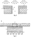
- Fig. 2 illustrates how the coating process of the printed circuit board 1 of the LED module 10 is performed.
- the basic idea of the method is the one-sided application, preferably spraying highly reflective materials on a printed circuit board 1 with at least one recess 2.
- the method may be an ink jet printing method.
- As a highly reflective layer 4 an ink based on highly reflective particles, for example made of ceramic, is then preferably applied as described above.
- a highly reflective layer 4 both on the surface 3 on the front of the LED module and the circuit board. 1 arises, as well as on the preferably inclined boundary walls 2a of the recess 2. However, can arise through the angle a different layer thickness. Typical unevennesses in recess 2, which are typically produced by drilling or other methods (eg, milling, laser cutting, punching, or the like), are in the range of 1 to 50 ⁇ m, preferably 10 to 50 ⁇ m.
- the highly reflective layer 4 is therefore preferably applied with a thickness between 5 and 50 ⁇ m.
- the highly reflective layer 4 is preferably the same thickness over the entire surface 3 of the printed circuit board 1, ie also on the boundary walls 2 a of the recess 2.
- the spray may be varied either deliberately or randomly in its direction and / or strength (i.e., spray rate of the material).
- the spray jet can also perform a continuous change in its direction, so that the same amount of material is sprayed in all directions at least over a predetermined spray area.
- common methods are conceivable, for. Example, a method that measures the current rate of the sprayed material, or a method that measures the layer thickness by means of a laser. The result of such a thickness measurement can be attributed to the device which carries out the method according to the invention. Based on the measured thickness of the highly reflective layer 4, the orientation of the spray jet and / or its thickness can then be changed in order to achieve a uniform layer over the entire surface 3.
- more than one spray for spraying the highly reflective layer 4 can be used on the circuit board 1.
- the orientations and / or strengths of the multiple spray jets can be changed either together or individually. It can also For example, a separate layer thickness measurement can be carried out in each spray area of the multiple spray jets.
- an extremely uniform highly reflective layer 4 could be formed by a multiple measurement of the layer thickness and a separate control of the individual spray jets.
- the highly reflective layer reliably obtains the desired layer thickness, preferably between 5 and 50 ⁇ m.
- the highly reflective layer 4 on the circuit board 1 is also prevents the back 1 of the circuit board is contaminated with the highly reflective material undefined. This could in fact mean that the attachment of the support plate 5 to the back of the circuit board 1 does not work optimally, that the strength of the connection is insufficient or that the back of the circuit board 1 has unevenness, which change the direction of the light emission and thus a negative Influence of the light output of the LED module 10 have.
- the method can also be used flexibly, so that printed circuit boards 1 can be coated with different recesses 2.
- boundary walls which are at different angles to the main plane of the circuit board 1 can be provided with a uniform layer 4. The process is fast and inexpensive and achieves a high yield.
- the carrier plate 5 is made of a material which is different from the printed circuit board material 1 and preferably consists of IMS (Insulated Metal Substrate).
- IMS Insulated Metal Substrate
- a color conversion material 7 can be arranged over the at least one LED chip 6.
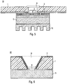
- the entire recess 2 can be filled with a color conversion material 7, as in Fig. 4 shown.
- a prefabricated plate 8 in the form of a ceramic color conversion plate or a phosphor provided glass over the opening of the recess 2 are placed.
- Such a color conversion plate 8 (for example made of ceramic, phosphorus in glass, phosphorus in silicone) can be externally prefabricated.
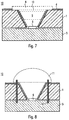
- a color conversion insert 9 can be provided, which advantageously has side walls which are adapted to the boundary walls 2a of the recess 2. That is, the side walls of the insert 9 should have the same angle as the boundary walls 2a of the recess 2 into which the color conversion insert 9 is inserted. In a preferred embodiment, the angle of the side walls of the color conversion insert is 45 °.
- Color conversion platelets 8 or color conversion inserts 9 can be manufactured by a corresponding cut from a color conversion layer, wherein in a preferred embodiment, in each case the cutting angle is 45 °.
- the color conversion insert 9 is inserted into the recess 2 of the printed circuit board 1. Since in a preferred embodiment, both the color conversion insert 9 and the boundary walls 2a of the circuit board 1 have an angle of 45 °, the color conversion insert can be inserted directly into the printed circuit board 1. At other angles between 10 ° and 90 ° advantageously have the side walls of the color conversion insert 9 just this angle of 10 ° to 90 °. By fixing the color conversion insert in the recess 2 of the printed circuit board 1 in particular, a precise alignment of the color conversion insert 9 with respect to the at least one LED chip 6 is possible.
- At least two color conversion elements are accommodated on the printed circuit board 1, such as in FIG Fig. 7
- it is also a color conversion plate 8 and a filling of the recess 2 with dye material as a combination of color conversion elements conceivable a color conversion platelet 8 and a color conversion insert.
- the two color conversion elements may consist of the same phosphor material.
- the concentration of the phosphor material in the two elements may be the same or different.
- the phosphor material of the chip 8 may also be different from the phosphor material of the insert 9.
- the two color conversion elements can be mounted directly above one another or separated from one another by a gap 16.
- the gap 16 may be filled with silicone or another at least partially transparent material.
- the gap 16 may also contain air.
- the structure of the LED module 10 can also be used to set a desired color temperature.
- a color conversion plate 8 and / or color conversion insert 9 is attached and the color location is measured in a CIE diagram. From a number of further color conversion platelets 8 and / or color conversion inserts 9 of different thickness, phosphorus concentration and / or phosphor composition that color conversion element is selected, with which the desired color temperature, d. H. the desired color locus in the CIE diagram can best be approximated.
- a secondary optic 11 (diffractive or refractive) or a secondary-optic element attached. This may be for example a lens or a globe top with at least one color conversion material and / or scattering particles.
- both the carrier plate 5 and the LED chips 6 must be aligned with respect to the printed circuit board 1, and the optional secondary optics 11 must be aligned with respect to the printed circuit board 1. This can lead to inaccuracies in the orientation of the secondary optics 11 relative to the at least one LED chip 6.
- the goal is to align both the carrier plate 5 and the optional secondary optics 11 with respect to the printed circuit board 1 in such a way that the smallest possible deviations in the alignment of the LED chips 6 with respect to the secondary optics 11 occur. This can generally be achieved by integrating one or more markers in the printed circuit board 1 and aligning both the carrier plate 5 and the secondary optics 11 against these markers during assembly of the board-in-board structure.
- a suitable positioning unit 12 for example, a marker pen
- This positioning unit 12 can also serve to align the secondary optics 11 with respect to the printed circuit board 1.
- the positioning unit 12 is designed such that both the printed circuit board 1 and the secondary optics 11 are placed on this positioning unit 12.
- An example would be at least one positioning pin 12, which protrudes from both the top and on the bottom of the circuit board 1, as in Fig. 8 is shown. Both the carrier plate 5 and the printed circuit board 1 are used in accordance with this at least one positioning pin 12.
- a positioning unit 13 as a cavity in the circuit board 1 executed.
- This cavity 13 may be continuous or partially filled with the printed circuit board material.
- the support plate 5 and the secondary optics 11 then have, for example, on their underside a pin-shaped extension 14 whose diameter is smaller than or equal to the diameter of the cavity 13 in the circuit board 1. Both the carrier plate 5 and the secondary optics 11 can be inserted into the cavity 13 with this pin-shaped extension 14.
- the printed circuit board 1 is aligned with the carrier plate 5 according to one of the above-mentioned examples by a positioning unit 12, 13 (for example a marker, a marker pin or a cavity).
- the diameter of the continuation 15 on the underside of the secondary optics 11 is only slightly smaller than the diameter of the recess 2 in the circuit board 1, so that the secondary optics 11 can be aligned by insertion into the recess 2 of the circuit board 1.
- the present invention provides a method for Coating a printed circuit board 1 of the LED module 10 before, with the light output of an LED module 10 can be significantly increased.
- This is achieved by additionally coating the printed circuit board 1 with a highly reflective layer 4 for better reflection of the light emitted by at least one LED chip 6.
- the coating is carried out as spraying, with which the layer 4 can be applied uniformly and contamination of other surfaces of the circuit board 1 or the support plate 5, on which the at least one LED chip 6 is mounted, can be prevented.
- the LED module 10 may further comprise at least one color conversion element 7, 8, 9, which is preferably mounted in or above the at least one recess 2 of the printed circuit board 1.
- positioning elements 12, 13 in the assembly of the LED module 10 in particular in the alignment of the circuit board 1 and the support plate 5 to each other help.
Landscapes
- Led Device Packages (AREA)
Description
- Die vorliegende Erfindung umfasst ein LED-Modul, das eine beschichtete Leiterplatte aufweist, und die beschichtete Leiterplatte selbst. Die beschichte Leiterplatte dient dazu einen Teil des seitlich von einem LED-Chip des LED-Moduls ausgestrahlten Lichts in Richtung der Normalachse des LED-Moduls zu richten. Insbesondere wird in der folgenden Erfindung ein Verfahren zum Beschichten einer Leiterplatte eines LED-Moduls vorgestellt.
- Es ist im Stand der Technik bekannt, eine Leiterplatte mit einer Ausnehmung in einem LED-Modul zu verbauen, um Licht, das von einem LED-Chip des LED-Moduls ausgestrahlt wird, nach außen zu reflektieren und eine Ausstrahlrichtung vorzugeben. Typischerweise ist eine solche Leiterplatte aus einem Kunststoff, dessen Oberfläche mit einer Kupferbahn überzogen ist. Die Kupferbahn ist dazu geeignet Licht zu reflektieren, die Effizienz ist aber gering. Der LED-Chip wird in dem LED-Modul so in der Ausnehmung der Leiterplatte platziert, dass er Licht von hinten durch die Ausnehmung hindurch aus dem LED-Modul heraus strahlt.
- Eine solche Kupferbahn auf der Oberfläche eines Kunststoffmaterials weist aber keine zufriedenstellenden Reflexionseigenschaften über den gesamten Spektralbereich des sichtbaren Lichts auf. Insbesondere im Spektralbereich von blauem Licht sind die Reflexionseigenschaften nicht ausreichend.
Beispielsweise bezieht sich dieUS 2011/0198628 A1 auf eine Multichip-Leuchtdioden (LED) -Packung aufweisend eine gedruckte Leiterplatte (PCB) mit einem sich verjüngenden Durchkontaktierungsloch und einer Schaltungsverbindungsleitung auf einer Oberfläche des PCBs.
Weiterhin bezieht sich dieUS 2009/0014732 A1 auf eine Chip-Typ Licht emittierende Vorrichtung und ein Verdrahtungssubstrat für die Vorrichtung. DieUS 2003/0193055 A1 bezieht sich auf eine Beleuchtungseinrichtung mit einer Leuchtdiode (LED). Die Vorrichtung enthält ein Metallsubstrat mit einer Oberfläche. Eine dielektrische Überzugsschicht ist auf der Oberfläche des Metallsubstrats überlagert. Eine lichtemittierende Diode (LED) ist auf der dielektrischen Überzugsschicht positioniert. Das Metallsubstrat dient als Wärmesenke für die von der LED während des Betriebs abgegebene Wärme.
DieWO 2012/002580 A1 und dieUS 2013/0099276 A1 beziehen sich auf eine LED-Lichtquellenvorrichtung umfassend: ein Substrat, eine Elektrode, die auf dem Substrat gebildet ist, eine weiße anorganische Resistschicht, die über dem Substrat abgeschieden ist, um eine Oberfläche davon, außer wo die Elektrode gebildet ist, abzudecken, und ein LED-Element, das mit der Elektrode verbunden ist, wobei die weiße anorganische Resistschicht feine weiße anorganische Partikel enthält, die in einem anorganischen Bindemittel dispergiert oder vermischt sind.
DieEP 1 978 566 A1 bezieht sich auf eine Lichtquellenvorrichtung umfassend: ein Substrat, das mindestens ein Paar von Elektroden, mindestens eine lichtemittierende Vorrichtung und ein transparentes Harz zum Abdichten der lichtemittierenden Vorrichtung umfasst, wobei eine weiße Resistschicht auf dem Substrat gebildet ist. - Die
US 2004/222433 A1 bezieht sich auf ein LED-Modul mit einem metallischen Träger der mit einer dicken keramischen Schicht überdeckt ist. Auf der Oberfläche dieser keramischen Schicht, in deren Ausnehmung eine Leuchtdiode angeordnet ist, kann eine reflektierende Schicht aufgesprüht werden. - Die vorliegende Erfindung schlägt deshalb als Grundidee vor, eine Oberfläche einer Leiterplatte mit einer hochreflektiven Schicht zu versehen. Allerdings sind herkömmliche Beschichtungsprozesse, wie beispielweise Siebdruck oder Curtain-Coating, dafür nicht gut geeignet, da sie keine zufriedenstellende gleichmäßige Beschichtung insbesondere der Begrenzungswände einer Ausnehmungen der Leiterplatte erzielen. Außerdem besteht die Gefahr, dass während solcher Prozesse die Rückseite der Leiterplatte mit dem aufzubringenden Material undefiniert kontaminiert wird. Siebdrucke können zwar zunächst für gröbere Strukturen verwendet werden, sind aber für feinere Strukturen ungeeignet.
- Die vorliegende Erfindung stellt sich zur Aufgabe alle genannten Nachteile des Stands der Technik zu verbessern. Insbesondere ist es eine Aufgabe der vorliegenden Erfindung, die Lichtausbeute eines LED-Moduls zu erhöhen und ein verbessertes Verfahren für das Beschichten einer Leiterplatte bereitzustellen. Dazu soll speziell eine Leiterplatte mit verbesserten Reflexionseigenschaften für ein LED-Modul hergestellt werden. Außerdem strebt die Erfindung an, die Nachteile gängiger Prozesse und Verfahren zu vermeiden. Insbesondere sollen die Begrenzungswände von Ausnehmungen in einer Leiterplatte mit guten Reflexionseigenschaften versehen werden.
- Die vorliegende Erfindung löst die oben genannten Aufgaben gemäß dem Gegenstand des unabhängigen Anspruchs 1. Die abhängigen Ansprüche entwickeln den Kerngedanken der Erfindung auf vorteilhafte Weise weiter.
- Die vorliegende Erfindung wird im Folgenden anhand der beigefügten Figuren im Detail beschrieben.
-
Fig. 1 zeigt ein LED-Modul gemäß einem Beispiel, das nicht Teil der Erfindung ist, mit einer beschichteten Leiterplatte. -
Fig. 2 zeigt wie eine Leiterplatte mit einem Verfahren gemäß einem Beispiel, das nicht Teil der Erfindung ist, beschichtet wird. -
Fig. 3 zeigt wie eine Leiterplatte mit einem Verfahren gemäß der vorliegenden Erfindung beschichtet wird. -
Fig. 4 zeigt ein LED-Modul gemäß einem Beispiel, das nicht Teil der Erfindung ist, mit einem Farbkonversionselement. -
Fig. 5 zeigt ein LED-Modul gemäß einem Beispiel, das nicht Teil der Erfindung ist, mit einem Farbkonversionselement. -
Fig. 6 zeigt ein LED-Modul gemäß einem Beispiel, das nicht Teil der Erfindung ist, mit Farbkonversionselement. -
Fig. 7 zeigt ein LED-Modul gemäß einem Beispiel, das nicht Teil der Erfindung ist, mit Farbkonversionselementen. -
Fig. 8 zeigt ein LED-Modul gemäß einem Beispiel, das nicht Teil der Erfindung ist, mit Positionierungselementen. -
Fig. 9 zeigt ein LED-Modul gemäß einem Beispiel, das nicht Teil der Erfindung ist, mit Positionierungselementen. -
Fig. 10 zeigt ein LED-Modul gemäß einem Beispiel, das nicht Teil der Erfindung ist, mit Positionierungselementen. -
Fig. 1 zeigt ein LED-Modul 10 gemäß einem Beispiel, das nicht Teil der Erfindung ist, sowie eine Leiterplatte 1. Die Leiterplatte 1 ist Teil des LED-Moduls 10, aber auch einzeln von dem Beispiel umfasst. Das LED-Modul 10 besteht aus wenigstens einem LED-Chip 6, der auf einer Trägerplatte 5 aufgebracht ist. Der wenigstens eine LED-Chip 6 kann zum Beispiel eine herkömmliche LED, eine OLED, eine Anordnung von mehreren LEDs oder eine LED-Strecke sein. Mehrere LEDs können entweder gleichfarbiges oder verschiedenfarbiges Licht aussenden. Zur Aufbringung des wenigstens einen LED-Chips 6 auf der Trägerplatte 5 kann dieser angelötet, angeklebt, aufgesteckt oder eingeklemmt werden. Dazu kann die Trägerplatte 5 gegebenenfalls geeignete Aufnahmemittel für den wenigstens einen LED-Chip 6 aufweisen. - Die Trägerplatte kann mehrschichtig aufgebaut sein. Die Trägerplatte 5 kann Materialien enthalten, die beispielweise Aluminium, Gold, Paladium, Nickel und/oder ein Dielektrikum enthalten. Der wenigstens eine LED-Chip 6 ist auf einer Oberfläche auf der Vorderseite der Trägerplatte 5, d. h. einer Oberfläche in Richtung der Ausstrahlseite des LED-Moduls 10, angebracht. Die Trägerplatte 5 ist wiederum an die Rückseite (in Lichtausstrahlrichtung gesehen) einer Leiterplatte 1 angebracht. Dazu kann die Trägerplatte 5 mit der Leiterplatte 1 verklebt, verlötet oder angesteckt werden. Ein leitfähiges Material der Trägerplatte 5, beispielweise eine Kupferschicht, kann dabei elektrisch mit der Leiterplatte 1 verbunden sein. An die Trägerplatte 5 kann rückseitig ferner eine Wärmesenke 16 angebracht sein, um Wärme von dem wenigstens einen LED-Chip 6 abzuführen. Die Wärmesenke kann beispielweise mit Kühllamellen ausgestattet sein.
- Der wenigstens eine LED-Chip 6 wird in wenigstens einer Ausnehmung 2 der Leiterplatte 1 platziert. Die Ausnehmung 2 kann eine Bohrung sein, oder kann eine Aussparung sein, die bereits während der Herstellung der Leiterplatte 1 gefertigt wird. Der wenigstens eine LED-Chip 6 wird so hinter oder in der Ausnehmung 2 positioniert, dass das von ihm ausgestrahlte Licht von hinten durch die Ausnehmung 2 der Leiterplatte 1 hindurch aus der Vorderseite des LED-Moduls 10 ausgestrahlt wird. Die Ausnehmung 2 in der Leiterplatte 1 dient als ein Mittel zum Reflektieren und zum Leiten des ausgestrahlten Lichts. Dadurch tritt das Licht gerichtet aus dem LED-Modul 10 aus. Die elektronische Ansteuerung des wenigstens einen LED-Chips 6 wird auf oder in der Trägerplatte 5 geführt.
- Die Leiterplatte 1 besteht vorzugsweise aus einem Kunststoffmaterial, beispielsweise aus einem FR4 glasfaserverstärkten Epoxid. Die Wärmeleitfähigkeit der Leiterplatte liegt vorzugsweise in einem Bereich von 0.1 bis 1 W/mK, mehr bevorzugt 0.2 bis 0.4 W/mK. Die Dicke der Leiterplatte kann zwischen 0.1 und 2 mm liegen. Die Leiterplatte 1 ist in der Regel auf einer ihrer Oberflächen (d. h. auf ihrer Vorderseite oder Rückseite) mit einer metallischen Bahn, beispielsweise einer Kupferbahn, überzogen. Es können aber auch andere geeignete Materialien wie Aluminium verwendet werden. Die metallische Bahn weist vorzugsweise eine Wärmeleitfähigkeit in einem Bereich von etwa 140 bis 500 W/mK auf, mehr bevorzugt etwa 300 bis 500 W/mK, noch mehr bevorzugt etwa 380 W/mK-420 W/mK. Zur Aufbringung der metallischen Bahn können herkömmliche Beschichtungsverfahren verwendet werden. Die metallische Bahn könnte auch zusätzlich zur Übermittlung von Strom oder Spannungssignalen an den wenigstens einen LED-Chip 6 verwendet werden.
- Die Begrenzungswände 2a in der wenigstens einen Ausnehmung 2 der Leiterplatte 1 nehmen einen Winkel mit der leitfähigen Oberfläche 3 der Leiterplatte 1 auf der Vorderseite des LED-Moduls 10 ein, der in einem Bereich von etwa 10° bis 90°, vorzugsweise in einem Bereich von 30° bis 60°, noch weiter bevorzugt 40° bis 50° liegt, oder am meisten bevorzugt 45° ist. Dadurch kann das von dem wenigstens einem LED-Chip 6 ausgesandte Licht ideal nach außen aus dem LED-Modul 10 reflektiert und geleitet werden.
- Um die Reflektivität der Leiterplatte 1 weiter zu erhöhen, insbesondere um die Reflexionseigenschaften über den gesamten Spektralbereich auszudehnen, wird die Oberfläche der Leiterplatte mit einer hochreflektiven Schicht 4 versehen. Die beschichtete Oberfläche kann die leitfähigen Kupferbahnen aufweisen. Die leitfähigen Kupferbahnen können aber auch auf einer anderen Oberfläche der Leiterplatte 1 als der beschichteten Oberfläche vorgesehen sein. Die hochreflektive Schicht 4 wird dabei sowohl auf die (optional leitfähige) Oberfläche 3 auf der Vorderseite des LED-Moduls 10 als auch auf der (optional leitfähigen) Oberfläche 3 auf den Begrenzungswänden 2a der Ausnehmung 2 aufgebracht. Die Schicht kann beispielsweise eine Schicht sein, die UV-Licht widersteht und Temperaturen bis zu mehreren 100° aushält, ohne ihre Reflexionseigenschaften zu verlieren. Dadurch wird die Zuverlässigkeit des LED-Moduls 10 erhöht und die Lebensdauer verlängert.
- Eine Möglichkeit eine solche hochreflektive Schicht 4 auszubilden ist dafür eine Tinte zu verwenden, die mit hochreflektiven Partikeln wie Keramikpartikeln versetzt ist. Diese Partikel sind vorzugsweise im Mikrometer- oder Nanometermaßstab, beispielweise 0.15 bis 0.45 µm. Die Schicht ist vorzugsweise 5 bis 50 µm dick, mehr bevorzugt 20 bis 30 µm. Die Schicht erhöht die Reflexionseigenschaften im gesamten sichtbaren Bereich insbesondere auch im blauen Spektralbereich. Dies ist vorteilhaft bei der Erzeugung von weißem Licht. Die oben genannte Tintenschicht kann beispielsweise mittels eines Tintenstrahldruckverfahrens auf die Leiterplatte 1 aufgebracht werden. Die Größe der Partikel in der Tinte ist so gewählt, dass die Viskosität der Tinte problemlos mit einem Tintenstrahldruckverfahren auf die Oberfläche 3 der Leiterplatte 1 gesprüht werden kann. Trotzdem ist die Menge an Partikeln in der Tinte auch so gewählt, dass sehr gute Reflexionseigenschaften über den gesamten gewünschten Spektralbereich erzielt werden. Die hochreflektive Schicht 4 wird gleichmäßig auch auf den schrägen Begrenzungswänden 2a aufgebracht. Auch wenn die Begrenzungswände sehr steil, d. h. annähernd 90° sind, kann mittels des Verfahrens der vorliegenden Erfindung eine gleichmäßige Beschichtung mit der hochreflektiven Schicht 4 erzielt werden.
-
Fig. 2 veranschaulicht wie das Beschichtungsverfahren der Leiterplatte 1 des LED-Moduls 10 ausgeführt wird. Die Grundidee des Verfahrens ist das einseitige Aufbringen, vorzugsweise Aufsprühen hochreflektiver Materialien auf eine Leiterplatte 1 mit wenigstens einer Ausnehmung 2. Wie oben beschrieben kann das Verfahren ein Tintenstrahldruckverfahren sein. Als hochreflektive Schicht 4 wird dann vorzugsweise wie oben beschrieben eine Tinte basierend auf hochreflektiven Partikeln beispielweise aus Keramik aufgebracht. - In
Fig. 2 ist zu sehen, wie durch einen gerichteten Aufsprühstrahl (dargestellt durch die Pfeile) eine hochreflektive Schicht 4 sowohl auf der Oberfläche 3 auf der Vorderseite des LED-Moduls bzw. der Leiterplatte 1 entsteht, als auch auf den vorzugsweise schräg stehenden Begrenzungswänden 2a der Ausnehmung 2. Allerdings kann durch den Winkel eine unterschiedliche Schichtdicke entstehen. Typische Unebenheiten in Ausnehmung 2, die typischerweise durch Bohrungen oder andere Verfahren (z. B. Fräsen, Laserschneiden, Stanzen o. ä.) hergestellt werden, sind im Bereich von 1 bis 50 µm, vorzugsweise 10 bis 50 µm. Vorzugsweise wird die hochreflektive Schicht 4 deshalb mit einer Dicke zwischen 5 und 50 µm aufgetragen. Die hochreflektive Schicht 4 ist vorzugsweise über die gesamte Oberfläche 3 der Leiterplatte 1, d. h. auch an den Begrenzungswänden 2a der Ausnehmung 2 gleich dick. - Dazu kann, wie in
Fig. 3 gezeigt, der Sprühstrahl (wiederum dargestellt durch die Pfeile) ausgerichtet, d. h. auch in seiner Richtung verändert werden. Somit wird es möglich z. B. auch sehr steil stehende Begrenzungswände 2a (beispielweise in einem Winkel von etwa 90°) mit einer hochreflektiven Schicht 4 zu versehen. Gleichzeitig ist es möglich, die Schicht über die komplette Oberfläche 3 der Leiterplatte 1 gleichmäßig dick aufzusprühen. - Der Sprühstrahl kann entweder gezielt oder zufällig in seiner Richtung und/oder Stärke (d. h. Sprührate des Materials) variiert werden. Der Sprühstrahl kann auch eine kontinuierliche Änderung seiner Richtung vollziehen, so dass wenigstens über einen vorgegebenen Sprühbereich in alle Richtungen gleich viel Material versprüht wird. Alternativ kann allerdings auch eine Schichtdickenmessung während des Aufsprühens durchgeführt werden. Dabei sind gängige Verfahren denkbar, z. B. ein Verfahren, das die derzeitige Rate des versprühten Materials misst, oder ein Verfahren, das die Schichtdicke mittels eines Lasers misst. Das Ergebnis einer solchen Dickenmessung kann der Vorrichtung, die das erfindungsgemäße Verfahren durchführt, zurückgeführt werden. Basierend auf der gemessenen Dicke der hochreflektiven Schicht 4 kann dann die Ausrichtung des Sprühstrahls und/oder dessen Stärke verändert werden, um eine gleichmäßige Schicht über die gesamte Oberfläche 3 zu erzielen.
- Wie in
Fig. 3 angedeutet, kann auch mehr als ein Sprühstrahl zum Aufsprühen der hochreflektiven Schicht 4 auf die Leiterplatte 1 verwendet werden. Die Ausrichtungen und/oder Stärken der mehreren Sprühstrahle können entweder gemeinsam oder individuell verändert werden. Es kann auch beispielsweise in jedem Sprühbereich der mehreren Sprühstrahle eine gesonderte Schichtdickenmessung durchgeführt werden. Somit könnte durch eine Mehrfachmessung der Schichtdicke und eine gesonderte Ansteuerung der einzelnen Sprühstrahle eine äußerst gleichmäßige hochreflektive Schicht 4 gebildet werden. - Insbesondere kann auch sichergestellt werden, dass die hochreflektive Schicht zuverlässig die gewünschte Schichtdicke, bevorzugt zwischen 5 und 50 µm, erhält.
- Durch das einseitig gerichtete Aufsprühverfahren der hochreflektiven Schicht 4 auf die Leiterplatte 1 wird auch verhindert, dass die Rückseite 1 der Leiterplatte mit dem hochreflektiven Material undefiniert kontaminiert wird. Dies könnte nämlich zur Folge haben, dass die Anbringung der Trägerplatte 5 an die Rückseite der Leiterplatte 1 nicht optimal funktioniert, dass die Festigkeit der Verbindung ungenügend ist oder dass die Rückseite der Leiterplatte 1 Unebenheiten aufweist, welche die Richtung der Lichtausstrahlung verändern und somit einen negativen Einfluss der Lichtausbeute des LED-Moduls 10 haben. Das Verfahren ist ferner flexibel einsetzbar, so dass Leiterplatten 1 mit verschiedenen Ausnehmungen 2 beschichtet werden können. Insbesondere Leiterplatten 1 mit Ausnehmungen 2 mit verschieden geformten Begrenzungswänden 2a, d. h. beispielsweise Begrenzungswänden die in verschiedenen Winkeln zur Hauptebene der Leiterplatte 1 stehen, können mit einer gleichmäßigen Schicht 4 versehen werden. Das Verfahren ist schnell und kostengünstig und erzielt eine hohe Ausbeute.
- Die Leiterplatte 1, welche wie beschrieben bevorzugt aus FR4 besteht, bildet einen sogenannten Board-in-Board Aufbau mit der Trägerplatte 5, die den wenigstens einen LED-Chip 6 trägt. Die Trägerplatte 5 besteht aus einem Material, welches vom Leiterplattenmaterial 1 verschieden ist und bevorzugt aus IMS (Insulated Metal Substrate) besteht. Über dem wenigstens einen LED-Chip 6 kann ein Farbkonversionsmaterial 7 angeordnet werden. Dazu kann in einer Ausführungsform die gesamte Ausnehmung 2 mit einem Farbkonversionsmaterial 7 ausgefüllt werden, wie in
Fig. 4 gezeigt. Alternativ oder zusätzlich kann wie inFig. 5 gezeigt auch ein vorgefertigtes Plättchen 8 in Form eines keramischen Farbkonversionsplättchens oder ein mit Phosphor versehenes Glas über die Öffnung der Ausnehmung 2 aufgesetzt werden. Ein solches Farbkonversionsplättchen 8 (beispielweise aus Keramik, Phosphor in Glas, Phosphor in Silikon) kann extern vorgefertigt werden. - Es kann auch wie in
Fig. 6 gezeigt ein Farbkonversionseinsatz 9 bereitgestellt werden, der vorteilhafterweise Seitenwände aufweist, die den Begrenzungswänden 2a der Ausnehmung 2 angepasst sind. Das heißt, die Seitenwände des Einsatzes 9 sollten denselben Winkel wie die Begrenzungswände 2a der Ausnehmung 2 aufweisen, in die der Farbkonversionseinsatz 9 eingesetzt wird. In einer bevorzugten Ausführung beträgt der Winkel der Seitenwände des Farbkonversionseinsatzes 45°. Farbkonversionsplättchen 8 oder Farbkonversionseinsätze 9 können durch ein entsprechendes Ausschneiden aus einer Farbkonversionsschicht gefertigt werden, wobei in einer bevorzugten Ausführung jeweils der Schnittwinkel 45° beträgt. - Der Farbkonversionseinsatz 9 wird in die Ausnehmung 2 der Leiterplatte 1 eingesetzt. Da in einem bevorzugten Ausführungsbeispiel sowohl der Farbkonversionseinsatz 9 als auch die Begrenzungswände 2a der Leiterplatte 1 einen Winkel von 45° besitzen, kann der Farbkonversionseinsatz direkt in die Leiterplatte 1 eingesetzt werden. Bei anderen Winkeln zwischen 10° und 90° weisen vorteilhafterweise die Seitenwände des Farbkonversionseinsatzes 9 eben diesen Winkel von 10° bis 90° auf. Durch die Fixierung des Farbkonversionseinsatzes in der Ausnehmung 2 der Leiterplatte 1 ist insbesondere auch eine genaue Ausrichtung des Farbkonversionseinsatzes 9 gegenüber dem wenigstens einen LED-Chip 6 möglich.
- In einer weiteren Ausführung sind auf der Leiterplatte 1 mindestens zwei Farbkonversionselemente untergebracht wie etwa in
Fig. 7 gezeigt ein Farbkonversionsplättchen 8 und ein Farbkonversionseinsatz 9. Es ist allerdings auch ein Farbkonversionsplättchen 8 und eine Füllung der Ausnehmung 2 mit Farbstoffmaterial als Kombination von Farbkonversionselementen denkbar. Die beiden Farbkonversionselemente können aus dem gleichen Phosphormaterial bestehen. Die Konzentration des Phosphormaterials in den beiden Elementen kann gleich oder unterschiedlich sein. Das Phosphormaterial des Plättchens 8 kann auch verschieden vom Phosphormaterial des Einsatzes 9. sein. Jedes der beiden Farbkonversionselemente kann dabei auch gleichzeitig mehr als nur eine Sorte Phosphormaterial enthalten. Die beiden Farbkonversionselemente können direkt übereinander angebracht sein oder durch einen Spalt 16 voneinander getrennt sein. Der Spalt 16 kann mit Silikon oder einem anderen zumindest teilweise transparenten Material gefüllt sein. Der Spalt 16 kann auch Luft enthalten. - In einer weiteren Ausführung kann der Aufbau des LED-Moduls 10 auch zur Einstellung einer gewünschten Farbtemperatur verwendet werden. Dazu wird zunächst ein Farbkonversionsplättchen 8 und/oder Farbkonversionseinsatz 9 angebracht und der Farbort in einem CIE-Diagramm gemessen. Aus einer Anzahl weiterer Farbkonversionsplättchen 8 und/oder Farbkonversionseinsätze 9 unterschiedlicher Dicke, Phosphorkonzentration und/oder Phosphorzusammensetzung wird jenes Farbkonversionselement ausgewählt, mit welchem die gewünschte Farbtemperatur, d. h. der gewünschte Farbort im CIE-Diagramm, am besten angenähert werden kann.
- Auf der Leiterplatte 1 kann über der Ausnehmung 2 wie in
Fig. 8 gezeigt auch eine weitere Sekundäroptik 11 (diffraktiv oder refraktiv) oder ein sekundäroptisches Element angebracht. Dies kann zum Beispiel eine Linse oder ein Globe-Top mit wenigstens einem Farbkonversionsmaterial und/oder Streupartikeln sein. - Für den Board-in-Board Aufbau muss sowohl die Trägerplatte 5 mit den LED-Chips 6 gegenüber der Leiterplatte 1 ausgerichtet werden, als auch die optionale Sekundäroptik 11 gegenüber der Leiterplatte 1 ausgerichtet werden. Dies kann dazu führen, dass es zu Ungenauigkeiten in der Ausrichtung der Sekundäroptik 11 gegenüber dem wenigstens einen LED-Chip 6 kommt. Ziel ist es aber, sowohl die Trägerplatte 5 als auch die optionale Sekundäroptik 11 gegenüber der Leiterplatte 1 so auszurichten, dass es zu möglichst geringen Abweichungen in der Ausrichtung der LED-Chips 6 gegenüber der Sekundäroptik 11 kommt. Dies kann im Allgemeinen dadurch erreicht werden, dass in der Leiterplatte 1 ein oder mehrere Marker integriert werden und sowohl die Trägerplatte 5 als auch die Sekundäroptik 11 während eines Zusammenbaus des Board-in-Board Aufbaus gegen diese Marker ausgerichtet werden.
- Insbesondere kann beispielweise wie in
Fig. 8 gezeigt eine geeignete Positionierungseinheit 12 (beispielweise ein Markerstift) verwendet werden, um die beiden Platten 1 und 5 gegeneinander auszurichten. Diese Positionierungseinheit 12 kann auch dazu dienen, die Sekundäroptik 11 gegenüber der Leiterplatte 1 auszurichten. In einer bevorzugten Ausführung ist die Positionierungseinheit 12 derartig gestaltet, dass sowohl die Leiterplatte 1 als auch die Sekundäroptik 11 auf diese Positionierungseinheit 12 aufgesetzt werden. Ein Beispiel wäre wenigstens ein Positionierungsstift 12, welcher sowohl an der Oberseite als auch auf der Unterseite aus der Leiterplatte 1 herausragt, wie es inFig. 8 dargestellt ist. Sowohl die Trägerplatte 5 als auch die Leiterplatte 1 werden entsprechend diesem wenigstens einen Positionierungsstift 12 eingesetzt. - In einer weiteren Ausführung ist wie in
Fig. 9 gezeigt eine Positionierungseinheit 13 als Hohlraum in der Leiterplatte 1 ausgeführt. Dieser Hohlraum 13 kann durchgehend sein oder teilweise mit dem Leiterplattenmaterial aufgefüllt sein. Die Trägerplatte 5 und die Sekundäroptik 11 weisen dann beispielweise an ihrer Unterseite einen stiftförmigen Fortsatz 14 auf, dessen Durchmesser kleiner oder gleich dem Durchmesser des Hohlraums 13 in der Leiterplatte 1 ist. Sowohl die Trägerplatte 5 als auch die Sekundäroptik 11 können mit diesem stiftförmigen Fortsatz 14 in den Hohlraum 13 eingesetzt werden. - In einer weiteren Ausführungsform wird wie in
Fig. 10 gezeigt die Leiterplatte 1 gegenüber der Trägerplatte 5 nach einem der oben angeführten Beispiele durch eine Positionierungseinheit 12, 13 (zum Beispiel ein Marker, ein Markierungsstift oder ein Hohlraum) ausgerichtet. Die Ausrichtung der Sekundäroptik 11 gegenüber der Leiterplatte 1 erfolgt hingegen dadurch, dass die Sekundäroptik 11 an ihrer Unterseite eine Fortsetzung 15 hat, deren Durchmesser kleiner oder gleich dem Durchmesser der Ausnehmung 2 in der Leiterplatte 1 ist. In einer bevorzugten Ausführung ist der Durchmesser der Fortsetzung 15 an der Unterseite der Sekundäroptik 11 nur unwesentlich kleiner als der Durchmesser der Ausnehmung 2 in der Leiterplatte 1, so dass die Sekundäroptik 11 durch Einsetzen in die Ausnehmung 2 der Leiterplatte 1 ausgerichtet werden kann. - Zusammenfassend stellt die vorliegende Erfindung ein Verfahren zur Beschichtung einer Leiterplatte 1 des LED-Moduls 10 vor, mit dem die Lichtausbeute eines LED-Moduls 10 deutlich erhöht werden kann. Dies wird dadurch erreicht, dass die Leiterplatte 1 zum besseren Reflektieren des von wenigstens einem LED-Chip 6 ausgestrahlten Lichts zusätzlich mit einer hochreflektiven Schicht 4 beschichtet wird. Das Beschichten wird dabei als Aufsprühvorgang durchgeführt, mit welchem die Schicht 4 gleichmäßig aufgetragen werden kann und eine Kontamination von anderen Flächen der Leiterplatte 1 oder der Trägerplatte 5, auf der der wenigstens eine LED-Chip 6 angebracht ist, verhindert werden kann. Das LED-Modul 10 kann ferner wenigstens ein Farbkonversionselement 7, 8, 9 aufweisen, das bevorzugt in oder über der wenigstens einen Ausnehmung 2 der Leiterplatte 1 angebracht wird. Schließlich können Positionierungselemente 12, 13 beim Zusammenbau des LED-Moduls 10 insbesondere bei der Ausrichtung der Leiterplatte 1 und der Trägerplatte 5 zueinander helfen.
Claims (6)
- Verfahren zum Beschichten einer Leiterplatte (1) eines LED-Moduls (10), wobei die Leiterplatte (1) wenigstens eine Ausnehmung (2) und eine Oberfläche (3) aufweist und auf die Oberfläche (3) eine hochreflektive Schicht (4) aufgesprüht wird, wobei die hochreflektive Schicht (4) mittels eines Sprühstrahls auf die Oberfläche (3) aufgesprüht wird,
dadurch gekennzeichnet, dass
der Sprühstrahl ausgerichtet werden kann, wobei die Ausrichtung des Sprühstrahls so gewählt und/oder variiert wird, dass die hochreflektive Schicht (4) auch gleichmäßig auf die seitlichen Begrenzungswände (2a) der wenigstens einen Ausnehmung (2) aufgesprüht wird. - Verfahren gemäß Anspruch 1, wobei die hochreflektive Schicht (4) durch ein Tintenstrahldruckverfahren aufgesprüht wird.
- Verfahren gemäß einem der Ansprüche 1 oder 2, wobei die hochreflektive Schicht (4) wenigstens aus einem UV-stabilen und/oder temperaturstabilen Material gebildet wird.
- Verfahren gemäß einem der Ansprüche 1 bis 3, wobei die hochreflektive Schicht (4) wenigstens aus einer Tinte gebildet wird, die auf hochreflektiven Partikeln basiert.
- Verfahren gemäß Anspruch 4, wobei die hochreflektiven Partikel einen Durchmesser aufweisen, der in einem Bereich von etwa 1 nm bis 2 µm liegt.
- Verfahren gemäß einem der Ansprüche 1 bis 5, wobei die hochreflektive Schicht (4) etwa 5 bis 50 µm dick aufgesprüht wird.
Applications Claiming Priority (3)
| Application Number | Priority Date | Filing Date | Title |
|---|---|---|---|
| DE102012207171 | 2012-04-30 | ||
| DE201210213178 DE102012213178A1 (de) | 2012-04-30 | 2012-07-26 | LED-Modul mit Leiterplatte |
| PCT/EP2013/054617 WO2013164112A1 (de) | 2012-04-30 | 2013-03-07 | Led-modul mit leiterplatte |
Publications (2)
| Publication Number | Publication Date |
|---|---|
| EP2845234A1 EP2845234A1 (de) | 2015-03-11 |
| EP2845234B1 true EP2845234B1 (de) | 2018-07-11 |
Family
ID=49323310
Family Applications (1)
| Application Number | Title | Priority Date | Filing Date |
|---|---|---|---|
| EP13712700.7A Not-in-force EP2845234B1 (de) | 2012-04-30 | 2013-03-07 | Verfahren zum beschichten einer leiterplatte eines led-moduls |
Country Status (5)
| Country | Link |
|---|---|
| US (1) | US20150115303A1 (de) |
| EP (1) | EP2845234B1 (de) |
| CN (1) | CN104412398B (de) |
| DE (1) | DE102012213178A1 (de) |
| WO (1) | WO2013164112A1 (de) |
Families Citing this family (5)
| Publication number | Priority date | Publication date | Assignee | Title |
|---|---|---|---|---|
| CN104776396A (zh) * | 2015-05-08 | 2015-07-15 | 李峰 | Led反射结构 |
| CN106671631A (zh) * | 2015-11-05 | 2017-05-17 | 深圳市华祥电路科技有限公司 | 电路板及其印刷方法 |
| US10667399B1 (en) * | 2018-11-27 | 2020-05-26 | Nokia Solutions And Networks Oy | Discrete component carrier |
| EP4160817A4 (de) * | 2020-05-26 | 2024-06-12 | KMW Inc. | Antennenvorrichtung |
| CN115836441A (zh) * | 2020-06-05 | 2023-03-21 | 株式会社Kmw | 多输入多输出天线装置 |
Citations (3)
| Publication number | Priority date | Publication date | Assignee | Title |
|---|---|---|---|---|
| US20040222433A1 (en) * | 2003-05-05 | 2004-11-11 | Lamina Ceramics | Light emitting diodes packaged for high temperature operation |
| EP1978566A1 (de) * | 2006-01-26 | 2008-10-08 | Sony Corporation | Lichtquellenvorrichtung und anzeigevorrichtung |
| WO2012002580A1 (ja) * | 2010-07-01 | 2012-01-05 | シチズンホールディングス株式会社 | Led光源装置及びその製造方法 |
Family Cites Families (20)
| Publication number | Priority date | Publication date | Assignee | Title |
|---|---|---|---|---|
| GB1245595A (en) * | 1967-09-11 | 1971-09-08 | Matsushita Electric Industrial Co Ltd | Energy-responsive luminescent device |
| US6048595A (en) * | 1996-09-18 | 2000-04-11 | Tdk Corporation | Printed articiles having light-storing printed layers |
| WO2001079361A1 (en) * | 2000-04-17 | 2001-10-25 | Matsushita Electric Industrial Co., Ltd. | Ink for display panel and method for producing plasma display panel using the same |
| US20030193055A1 (en) * | 2002-04-10 | 2003-10-16 | Martter Robert H. | Lighting device and method |
| TW557590B (en) * | 2002-09-04 | 2003-10-11 | Opto Tech Corp | Light-emitting device array |
| US7300182B2 (en) * | 2003-05-05 | 2007-11-27 | Lamina Lighting, Inc. | LED light sources for image projection systems |
| KR100624416B1 (ko) * | 2003-12-23 | 2006-09-18 | 삼성전자주식회사 | 플립칩형 질화물계 발광소자 및 그 제조방법 |
| JP3956965B2 (ja) * | 2004-09-07 | 2007-08-08 | 日立エーアイシー株式会社 | チップ部品型発光装置及びそのための配線基板 |
| FR2877083B1 (fr) * | 2004-10-25 | 2007-01-26 | Bic Sa Soc | Capteur optique de proximite pour instrument de projection de liquide et instrument de projection de liquide equipe d'un tel capteur |
| DE102005059524A1 (de) * | 2005-09-30 | 2007-04-05 | Osram Opto Semiconductors Gmbh | Gehäuse für ein elektromagnetische Strahlung emittierendes optoelektronisches Bauelement, Bauelement und Verfahren zum Herstellen eines Gehäuses oder eines Bauelements |
| JP4828248B2 (ja) * | 2006-02-16 | 2011-11-30 | 新光電気工業株式会社 | 発光装置及びその製造方法 |
| US7901776B2 (en) * | 2006-12-29 | 2011-03-08 | 3M Innovative Properties Company | Plasma deposited microporous carbon material |
| KR20080067158A (ko) * | 2007-01-15 | 2008-07-18 | 삼성전자주식회사 | 표시장치 |
| JP2008187030A (ja) * | 2007-01-30 | 2008-08-14 | Stanley Electric Co Ltd | 発光装置 |
| US20090141355A1 (en) * | 2007-09-25 | 2009-06-04 | Opsec Security Group, Inc. | Security device, reflective layer therefor, and associated method |
| KR101006357B1 (ko) * | 2008-10-21 | 2011-01-10 | 주식회사 케이엠더블유 | 멀티칩 엘이디 패키지 |
| EP2448026A4 (de) * | 2009-06-26 | 2013-08-14 | Asahi Rubber Inc | Material zur reflektion von weisser farbe und herstellungsverfahren dafür |
| US20120037935A1 (en) * | 2010-08-13 | 2012-02-16 | Wen-Kun Yang | Substrate Structure of LED (light emitting diode) Packaging and Method of the same |
| US20120212976A1 (en) * | 2011-02-22 | 2012-08-23 | Kocam International Co., Ltd. | Integrated backlight module with good heat equalization and heat dissipation performance |
| JP5817297B2 (ja) * | 2011-06-03 | 2015-11-18 | 東芝ライテック株式会社 | 発光装置及び照明装置 |
-
2012
- 2012-07-26 DE DE201210213178 patent/DE102012213178A1/de not_active Withdrawn
-
2013
- 2013-03-07 US US14/398,027 patent/US20150115303A1/en not_active Abandoned
- 2013-03-07 WO PCT/EP2013/054617 patent/WO2013164112A1/de not_active Ceased
- 2013-03-07 CN CN201380034849.4A patent/CN104412398B/zh not_active Expired - Fee Related
- 2013-03-07 EP EP13712700.7A patent/EP2845234B1/de not_active Not-in-force
Patent Citations (4)
| Publication number | Priority date | Publication date | Assignee | Title |
|---|---|---|---|---|
| US20040222433A1 (en) * | 2003-05-05 | 2004-11-11 | Lamina Ceramics | Light emitting diodes packaged for high temperature operation |
| EP1978566A1 (de) * | 2006-01-26 | 2008-10-08 | Sony Corporation | Lichtquellenvorrichtung und anzeigevorrichtung |
| WO2012002580A1 (ja) * | 2010-07-01 | 2012-01-05 | シチズンホールディングス株式会社 | Led光源装置及びその製造方法 |
| US20130099276A1 (en) * | 2010-07-01 | 2013-04-25 | Citizen Electronics Co., Ltd. | Led light source device and manufacturing method for the same |
Also Published As
| Publication number | Publication date |
|---|---|
| EP2845234A1 (de) | 2015-03-11 |
| WO2013164112A1 (de) | 2013-11-07 |
| CN104412398B (zh) | 2017-10-24 |
| US20150115303A1 (en) | 2015-04-30 |
| CN104412398A (zh) | 2015-03-11 |
| DE102012213178A1 (de) | 2013-10-31 |
Similar Documents
| Publication | Publication Date | Title |
|---|---|---|
| DE102006009955B4 (de) | Weiße Lichtquelle und Beleuchtungsvorrichtung, die die weiße Lichtquelle verwendet | |
| EP1843394B1 (de) | Halbleiter-strahlungsquelle und lichthärtgerät mit dieser | |
| DE102016119002B4 (de) | Optoelektronisches bauelement und verfahren zum herstellen eines optoelektronischen bauelements | |
| WO2007076819A1 (de) | Beleuchtungseinrichtung | |
| DE112015004631B4 (de) | Laserbauelement und Verfahren zu seiner Herstellung | |
| DE112018002439B4 (de) | Abdeckung für ein optoelektronisches Bauelement und optoelektronisches Bauteil | |
| EP2845233B1 (de) | Led-modul | |
| EP2561270A1 (de) | Flächenlichtquelle | |
| EP2845234A1 (de) | Led-modul mit leiterplatte | |
| DE102017127597B4 (de) | Optoelektronisches bauelement und verfahren zum herstellen eines optoelektronischen bauelements | |
| DE102014113844B4 (de) | Verfahren zum Herstellen eines optoelektronischen Bauelements und optoelektronisches Bauelement | |
| EP1696404A1 (de) | Leuchtdiodenanordnung | |
| DE102016116617A1 (de) | Lichtemittierende Vorrichtung | |
| DE102010029529A1 (de) | Bauelementeträger für eine Leuchtvorrichtung, Leuchtvorrichtung, Verfahren zum Herstellen eines Bauelementeträgers und Verfahren zum Bestücken eines Bauelementeträgers | |
| DE112018006755B4 (de) | Eine Fahrzeuglampe, die eine lichtemittierende Halbleitervorrichtung verwendet | |
| DE102015206797A1 (de) | Leuchtmittel mit LEDs | |
| WO2015067612A1 (de) | Optoelektronisches bauelement, optoelektronische anordnung, verfahren zum herstellen eines optischen elements und verfahren zum herstellen eines optoelektronischen bauelements | |
| EP2238487A2 (de) | Lichtleitereinrichtung, beleuchtungsvorrichtung mit einer solchen lichtleitereinrichtung und verfahren zur herstellung einer solchen lichtleitereinrichtung | |
| DE102017130764B4 (de) | Vorrichtung mit Halbleiterchips auf einem Primärträger und Verfahren zur Herstellung einer solchen Vorrichtung | |
| DE102010010750A1 (de) | Multilayersubstrat mit flächigem Leuchtkörper | |
| DE102015206805A1 (de) | Leuchtmittel mit LEDs | |
| DE102014100584A1 (de) | Verfahren zum Herstellen von optoelektronischen Halbleiterbauteilen und optoelektronisches Halbleiterbauteil | |
| DE102018120637A1 (de) | Leiterplatte und verfahren zur herstellung einer leiterplatte mit mindestens einem in die leiterplatte integrierten optoelektronischen bauelement | |
| EP1634332A1 (de) | Isoliertes metallsubstrat mit wenigstens einer leuchtdiode, leuchtdiodenmatrix und herstellungsverfahren | |
| WO2016165855A1 (de) | LEUCHTMITTEL MIT LEDs |
Legal Events
| Date | Code | Title | Description |
|---|---|---|---|
| PUAI | Public reference made under article 153(3) epc to a published international application that has entered the european phase |
Free format text: ORIGINAL CODE: 0009012 |
|
| 17P | Request for examination filed |
Effective date: 20141029 |
|
| AK | Designated contracting states |
Kind code of ref document: A1 Designated state(s): AL AT BE BG CH CY CZ DE DK EE ES FI FR GB GR HR HU IE IS IT LI LT LU LV MC MK MT NL NO PL PT RO RS SE SI SK SM TR |
|
| AX | Request for extension of the european patent |
Extension state: BA ME |
|
| DAX | Request for extension of the european patent (deleted) | ||
| STAA | Information on the status of an ep patent application or granted ep patent |
Free format text: STATUS: EXAMINATION IS IN PROGRESS |
|
| 17Q | First examination report despatched |
Effective date: 20170110 |
|
| GRAP | Despatch of communication of intention to grant a patent |
Free format text: ORIGINAL CODE: EPIDOSNIGR1 |
|
| STAA | Information on the status of an ep patent application or granted ep patent |
Free format text: STATUS: GRANT OF PATENT IS INTENDED |
|
| RIC1 | Information provided on ipc code assigned before grant |
Ipc: H01L 33/60 20100101AFI20180315BHEP |
|
| INTG | Intention to grant announced |
Effective date: 20180406 |
|
| GRAA | (expected) grant |
Free format text: ORIGINAL CODE: 0009210 |
|
| STAA | Information on the status of an ep patent application or granted ep patent |
Free format text: STATUS: THE PATENT HAS BEEN GRANTED |
|
| AK | Designated contracting states |
Kind code of ref document: B1 Designated state(s): AL AT BE BG CH CY CZ DE DK EE ES FI FR GB GR HR HU IE IS IT LI LT LU LV MC MK MT NL NO PL PT RO RS SE SI SK SM TR |
|
| REG | Reference to a national code |
Ref country code: GB Ref legal event code: FG4D Free format text: NOT ENGLISH |
|
| REG | Reference to a national code |
Ref country code: CH Ref legal event code: EP |
|
| REG | Reference to a national code |
Ref country code: AT Ref legal event code: REF Ref document number: 1017820 Country of ref document: AT Kind code of ref document: T Effective date: 20180715 |
|
| GRAS | Grant fee paid |
Free format text: ORIGINAL CODE: EPIDOSNIGR3 |
|
| REG | Reference to a national code |
Ref country code: IE Ref legal event code: FG4D Free format text: LANGUAGE OF EP DOCUMENT: GERMAN |
|
| REG | Reference to a national code |
Ref country code: DE Ref legal event code: R096 Ref document number: 502013010583 Country of ref document: DE |
|
| REG | Reference to a national code |
Ref country code: NL Ref legal event code: MP Effective date: 20180711 |
|
| REG | Reference to a national code |
Ref country code: LT Ref legal event code: MG4D |
|
| PG25 | Lapsed in a contracting state [announced via postgrant information from national office to epo] |
Ref country code: NL Free format text: LAPSE BECAUSE OF FAILURE TO SUBMIT A TRANSLATION OF THE DESCRIPTION OR TO PAY THE FEE WITHIN THE PRESCRIBED TIME-LIMIT Effective date: 20180711 |
|
| PG25 | Lapsed in a contracting state [announced via postgrant information from national office to epo] |
Ref country code: IS Free format text: LAPSE BECAUSE OF FAILURE TO SUBMIT A TRANSLATION OF THE DESCRIPTION OR TO PAY THE FEE WITHIN THE PRESCRIBED TIME-LIMIT Effective date: 20181111 Ref country code: RS Free format text: LAPSE BECAUSE OF FAILURE TO SUBMIT A TRANSLATION OF THE DESCRIPTION OR TO PAY THE FEE WITHIN THE PRESCRIBED TIME-LIMIT Effective date: 20180711 Ref country code: PL Free format text: LAPSE BECAUSE OF FAILURE TO SUBMIT A TRANSLATION OF THE DESCRIPTION OR TO PAY THE FEE WITHIN THE PRESCRIBED TIME-LIMIT Effective date: 20180711 Ref country code: LT Free format text: LAPSE BECAUSE OF FAILURE TO SUBMIT A TRANSLATION OF THE DESCRIPTION OR TO PAY THE FEE WITHIN THE PRESCRIBED TIME-LIMIT Effective date: 20180711 Ref country code: SE Free format text: LAPSE BECAUSE OF FAILURE TO SUBMIT A TRANSLATION OF THE DESCRIPTION OR TO PAY THE FEE WITHIN THE PRESCRIBED TIME-LIMIT Effective date: 20180711 Ref country code: BG Free format text: LAPSE BECAUSE OF FAILURE TO SUBMIT A TRANSLATION OF THE DESCRIPTION OR TO PAY THE FEE WITHIN THE PRESCRIBED TIME-LIMIT Effective date: 20181011 Ref country code: FI Free format text: LAPSE BECAUSE OF FAILURE TO SUBMIT A TRANSLATION OF THE DESCRIPTION OR TO PAY THE FEE WITHIN THE PRESCRIBED TIME-LIMIT Effective date: 20180711 Ref country code: NO Free format text: LAPSE BECAUSE OF FAILURE TO SUBMIT A TRANSLATION OF THE DESCRIPTION OR TO PAY THE FEE WITHIN THE PRESCRIBED TIME-LIMIT Effective date: 20181011 Ref country code: GR Free format text: LAPSE BECAUSE OF FAILURE TO SUBMIT A TRANSLATION OF THE DESCRIPTION OR TO PAY THE FEE WITHIN THE PRESCRIBED TIME-LIMIT Effective date: 20181012 |
|
| PG25 | Lapsed in a contracting state [announced via postgrant information from national office to epo] |
Ref country code: HR Free format text: LAPSE BECAUSE OF FAILURE TO SUBMIT A TRANSLATION OF THE DESCRIPTION OR TO PAY THE FEE WITHIN THE PRESCRIBED TIME-LIMIT Effective date: 20180711 Ref country code: ES Free format text: LAPSE BECAUSE OF FAILURE TO SUBMIT A TRANSLATION OF THE DESCRIPTION OR TO PAY THE FEE WITHIN THE PRESCRIBED TIME-LIMIT Effective date: 20180711 Ref country code: LV Free format text: LAPSE BECAUSE OF FAILURE TO SUBMIT A TRANSLATION OF THE DESCRIPTION OR TO PAY THE FEE WITHIN THE PRESCRIBED TIME-LIMIT Effective date: 20180711 Ref country code: AL Free format text: LAPSE BECAUSE OF FAILURE TO SUBMIT A TRANSLATION OF THE DESCRIPTION OR TO PAY THE FEE WITHIN THE PRESCRIBED TIME-LIMIT Effective date: 20180711 |
|
| REG | Reference to a national code |
Ref country code: DE Ref legal event code: R097 Ref document number: 502013010583 Country of ref document: DE |
|
| PG25 | Lapsed in a contracting state [announced via postgrant information from national office to epo] |
Ref country code: IT Free format text: LAPSE BECAUSE OF FAILURE TO SUBMIT A TRANSLATION OF THE DESCRIPTION OR TO PAY THE FEE WITHIN THE PRESCRIBED TIME-LIMIT Effective date: 20180711 Ref country code: RO Free format text: LAPSE BECAUSE OF FAILURE TO SUBMIT A TRANSLATION OF THE DESCRIPTION OR TO PAY THE FEE WITHIN THE PRESCRIBED TIME-LIMIT Effective date: 20180711 Ref country code: CZ Free format text: LAPSE BECAUSE OF FAILURE TO SUBMIT A TRANSLATION OF THE DESCRIPTION OR TO PAY THE FEE WITHIN THE PRESCRIBED TIME-LIMIT Effective date: 20180711 Ref country code: EE Free format text: LAPSE BECAUSE OF FAILURE TO SUBMIT A TRANSLATION OF THE DESCRIPTION OR TO PAY THE FEE WITHIN THE PRESCRIBED TIME-LIMIT Effective date: 20180711 |
|
| PLBE | No opposition filed within time limit |
Free format text: ORIGINAL CODE: 0009261 |
|
| STAA | Information on the status of an ep patent application or granted ep patent |
Free format text: STATUS: NO OPPOSITION FILED WITHIN TIME LIMIT |
|
| PG25 | Lapsed in a contracting state [announced via postgrant information from national office to epo] |
Ref country code: SM Free format text: LAPSE BECAUSE OF FAILURE TO SUBMIT A TRANSLATION OF THE DESCRIPTION OR TO PAY THE FEE WITHIN THE PRESCRIBED TIME-LIMIT Effective date: 20180711 Ref country code: SK Free format text: LAPSE BECAUSE OF FAILURE TO SUBMIT A TRANSLATION OF THE DESCRIPTION OR TO PAY THE FEE WITHIN THE PRESCRIBED TIME-LIMIT Effective date: 20180711 Ref country code: DK Free format text: LAPSE BECAUSE OF FAILURE TO SUBMIT A TRANSLATION OF THE DESCRIPTION OR TO PAY THE FEE WITHIN THE PRESCRIBED TIME-LIMIT Effective date: 20180711 |
|
| PGFP | Annual fee paid to national office [announced via postgrant information from national office to epo] |
Ref country code: AT Payment date: 20190328 Year of fee payment: 7 |
|
| 26N | No opposition filed |
Effective date: 20190412 |
|
| PG25 | Lapsed in a contracting state [announced via postgrant information from national office to epo] |
Ref country code: SI Free format text: LAPSE BECAUSE OF FAILURE TO SUBMIT A TRANSLATION OF THE DESCRIPTION OR TO PAY THE FEE WITHIN THE PRESCRIBED TIME-LIMIT Effective date: 20180711 |
|
| PG25 | Lapsed in a contracting state [announced via postgrant information from national office to epo] |
Ref country code: MC Free format text: LAPSE BECAUSE OF FAILURE TO SUBMIT A TRANSLATION OF THE DESCRIPTION OR TO PAY THE FEE WITHIN THE PRESCRIBED TIME-LIMIT Effective date: 20180711 |
|
| REG | Reference to a national code |
Ref country code: CH Ref legal event code: PL |
|
| PG25 | Lapsed in a contracting state [announced via postgrant information from national office to epo] |
Ref country code: LU Free format text: LAPSE BECAUSE OF NON-PAYMENT OF DUE FEES Effective date: 20190307 |
|
| REG | Reference to a national code |
Ref country code: BE Ref legal event code: MM Effective date: 20190331 |
|
| PG25 | Lapsed in a contracting state [announced via postgrant information from national office to epo] |
Ref country code: LI Free format text: LAPSE BECAUSE OF NON-PAYMENT OF DUE FEES Effective date: 20190331 Ref country code: CH Free format text: LAPSE BECAUSE OF NON-PAYMENT OF DUE FEES Effective date: 20190331 Ref country code: IE Free format text: LAPSE BECAUSE OF NON-PAYMENT OF DUE FEES Effective date: 20190307 |
|
| PG25 | Lapsed in a contracting state [announced via postgrant information from national office to epo] |
Ref country code: BE Free format text: LAPSE BECAUSE OF NON-PAYMENT OF DUE FEES Effective date: 20190331 |
|
| PG25 | Lapsed in a contracting state [announced via postgrant information from national office to epo] |
Ref country code: TR Free format text: LAPSE BECAUSE OF FAILURE TO SUBMIT A TRANSLATION OF THE DESCRIPTION OR TO PAY THE FEE WITHIN THE PRESCRIBED TIME-LIMIT Effective date: 20180711 |
|
| PG25 | Lapsed in a contracting state [announced via postgrant information from national office to epo] |
Ref country code: MT Free format text: LAPSE BECAUSE OF FAILURE TO SUBMIT A TRANSLATION OF THE DESCRIPTION OR TO PAY THE FEE WITHIN THE PRESCRIBED TIME-LIMIT Effective date: 20180711 Ref country code: PT Free format text: LAPSE BECAUSE OF FAILURE TO SUBMIT A TRANSLATION OF THE DESCRIPTION OR TO PAY THE FEE WITHIN THE PRESCRIBED TIME-LIMIT Effective date: 20181111 |
|
| REG | Reference to a national code |
Ref country code: AT Ref legal event code: MM01 Ref document number: 1017820 Country of ref document: AT Kind code of ref document: T Effective date: 20200307 |
|
| PG25 | Lapsed in a contracting state [announced via postgrant information from national office to epo] |
Ref country code: AT Free format text: LAPSE BECAUSE OF NON-PAYMENT OF DUE FEES Effective date: 20200307 |
|
| REG | Reference to a national code |
Ref country code: DE Ref legal event code: R084 Ref document number: 502013010583 Country of ref document: DE |
|
| PG25 | Lapsed in a contracting state [announced via postgrant information from national office to epo] |
Ref country code: CY Free format text: LAPSE BECAUSE OF FAILURE TO SUBMIT A TRANSLATION OF THE DESCRIPTION OR TO PAY THE FEE WITHIN THE PRESCRIBED TIME-LIMIT Effective date: 20180711 |
|
| PG25 | Lapsed in a contracting state [announced via postgrant information from national office to epo] |
Ref country code: HU Free format text: LAPSE BECAUSE OF FAILURE TO SUBMIT A TRANSLATION OF THE DESCRIPTION OR TO PAY THE FEE WITHIN THE PRESCRIBED TIME-LIMIT; INVALID AB INITIO Effective date: 20130307 |
|
| REG | Reference to a national code |
Ref country code: DE Ref legal event code: R081 Ref document number: 502013010583 Country of ref document: DE Owner name: TRIDONIC GMBH & CO KG, AT Free format text: FORMER OWNERS: AT & S AUSTRIA TECHNOLOGIE & SYSTEMTECHNIK AKTIENGESELLSCHAFT, LEOBEN-HINTERBERG, AT; TRIDONIC JENNERSDORF GMBH, JENNERSDORF, AT Ref country code: DE Ref legal event code: R081 Ref document number: 502013010583 Country of ref document: DE Owner name: AT & S AUSTRIA TECHNOLOGIE & SYSTEMTECHNIK AKT, AT Free format text: FORMER OWNERS: AT & S AUSTRIA TECHNOLOGIE & SYSTEMTECHNIK AKTIENGESELLSCHAFT, LEOBEN-HINTERBERG, AT; TRIDONIC JENNERSDORF GMBH, JENNERSDORF, AT |
|
| PGFP | Annual fee paid to national office [announced via postgrant information from national office to epo] |
Ref country code: GB Payment date: 20220322 Year of fee payment: 10 |
|
| PGFP | Annual fee paid to national office [announced via postgrant information from national office to epo] |
Ref country code: FR Payment date: 20220325 Year of fee payment: 10 |
|
| PG25 | Lapsed in a contracting state [announced via postgrant information from national office to epo] |
Ref country code: MK Free format text: LAPSE BECAUSE OF FAILURE TO SUBMIT A TRANSLATION OF THE DESCRIPTION OR TO PAY THE FEE WITHIN THE PRESCRIBED TIME-LIMIT Effective date: 20180711 |
|
| PGFP | Annual fee paid to national office [announced via postgrant information from national office to epo] |
Ref country code: DE Payment date: 20230328 Year of fee payment: 11 |
|
| GBPC | Gb: european patent ceased through non-payment of renewal fee |
Effective date: 20230307 |
|
| P01 | Opt-out of the competence of the unified patent court (upc) registered |
Effective date: 20231130 |
|
| PG25 | Lapsed in a contracting state [announced via postgrant information from national office to epo] |
Ref country code: GB Free format text: LAPSE BECAUSE OF NON-PAYMENT OF DUE FEES Effective date: 20230307 |
|
| PG25 | Lapsed in a contracting state [announced via postgrant information from national office to epo] |
Ref country code: GB Free format text: LAPSE BECAUSE OF NON-PAYMENT OF DUE FEES Effective date: 20230307 Ref country code: FR Free format text: LAPSE BECAUSE OF NON-PAYMENT OF DUE FEES Effective date: 20230331 |
|
| REG | Reference to a national code |
Ref country code: DE Ref legal event code: R119 Ref document number: 502013010583 Country of ref document: DE |
|
| PG25 | Lapsed in a contracting state [announced via postgrant information from national office to epo] |
Ref country code: DE Free format text: LAPSE BECAUSE OF NON-PAYMENT OF DUE FEES Effective date: 20241001 |
|
| PG25 | Lapsed in a contracting state [announced via postgrant information from national office to epo] |
Ref country code: DE Free format text: LAPSE BECAUSE OF NON-PAYMENT OF DUE FEES Effective date: 20241001 |