EP2843825A2 - Motor controller - Google Patents
Motor controller Download PDFInfo
- Publication number
- EP2843825A2 EP2843825A2 EP14182196.7A EP14182196A EP2843825A2 EP 2843825 A2 EP2843825 A2 EP 2843825A2 EP 14182196 A EP14182196 A EP 14182196A EP 2843825 A2 EP2843825 A2 EP 2843825A2
- Authority
- EP
- European Patent Office
- Prior art keywords
- output
- detected
- angle detection
- detected output
- magnetic detector
- Prior art date
- Legal status (The legal status is an assumption and is not a legal conclusion. Google has not performed a legal analysis and makes no representation as to the accuracy of the status listed.)
- Granted
Links
Images



Classifications
-
- H—ELECTRICITY
- H02—GENERATION; CONVERSION OR DISTRIBUTION OF ELECTRIC POWER
- H02P—CONTROL OR REGULATION OF ELECTRIC MOTORS, ELECTRIC GENERATORS OR DYNAMO-ELECTRIC CONVERTERS; CONTROLLING TRANSFORMERS, REACTORS OR CHOKE COILS
- H02P6/00—Arrangements for controlling synchronous motors or other dynamo-electric motors using electronic commutation dependent on the rotor position; Electronic commutators therefor
- H02P6/10—Arrangements for controlling torque ripple, e.g. providing reduced torque ripple
-
- G—PHYSICS
- G01—MEASURING; TESTING
- G01R—MEASURING ELECTRIC VARIABLES; MEASURING MAGNETIC VARIABLES
- G01R33/00—Arrangements or instruments for measuring magnetic variables
- G01R33/02—Measuring direction or magnitude of magnetic fields or magnetic flux
- G01R33/06—Measuring direction or magnitude of magnetic fields or magnetic flux using galvano-magnetic devices
- G01R33/09—Magnetoresistive devices
-
- H—ELECTRICITY
- H02—GENERATION; CONVERSION OR DISTRIBUTION OF ELECTRIC POWER
- H02P—CONTROL OR REGULATION OF ELECTRIC MOTORS, ELECTRIC GENERATORS OR DYNAMO-ELECTRIC CONVERTERS; CONTROLLING TRANSFORMERS, REACTORS OR CHOKE COILS
- H02P6/00—Arrangements for controlling synchronous motors or other dynamo-electric motors using electronic commutation dependent on the rotor position; Electronic commutators therefor
- H02P6/12—Monitoring commutation; Providing indication of commutation failure
-
- H—ELECTRICITY
- H02—GENERATION; CONVERSION OR DISTRIBUTION OF ELECTRIC POWER
- H02P—CONTROL OR REGULATION OF ELECTRIC MOTORS, ELECTRIC GENERATORS OR DYNAMO-ELECTRIC CONVERTERS; CONTROLLING TRANSFORMERS, REACTORS OR CHOKE COILS
- H02P6/00—Arrangements for controlling synchronous motors or other dynamo-electric motors using electronic commutation dependent on the rotor position; Electronic commutators therefor
- H02P6/14—Electronic commutators
- H02P6/16—Circuit arrangements for detecting position
Definitions
- the present invention relates to a motor controller which controls three-phase driving power by using an analog output which is analogous to a linear function that is proportional to the rotation angle of a rotation shaft.
- motor controllers which control a three-phase motor, three-phase driving power for the phase U, the phase V, and the phase W is supplied to motor coils in accordance with the rotation phase of a motor.
- an arithmetic processing unit calculates a motor control signal, and a logic circuit supplied with the motor control signal calculates a driving signal for each of the phases of the three-phase motor.
- a pre-driver circuit is controlled on the basis of the driving signal, and the three-phase motor is controlled.
- the motor controller described in WO2012/102113 A1 generates a driving signal for driving the three-phase motor, through digital calculation, resulting in a complicated circuit configuration.
- the digital calculation takes time. Accordingly, when the motor rotates at high speed, there arises a problem in that the digital calculation fails to be performed at a speed in line with the rotational speed.
- the present invention provides a motor controller which enables three-phase driving power to be switched by using an analog output obtained by using a simple circuit configuration, and which enables the switching to be performed at a speed in line with high-speed rotation.
- a motor controller including a motor driver and an angle detection device.
- the motor driver supplies three-phase driving power to a motor coil.
- the angle detection device detects a rotation angle of a rotation shaft.
- the angle detection device includes a rotating magnetic field, a first magnetic detector, a second magnetic detector, and an analog mixer.
- the rotating magnetic field is formed in accordance with the rotation of the rotation shaft.
- the first magnetic detector obtains a detected output analogous to a sine wave which is a rotation angle function for the rotating magnetic field.
- the second magnetic detector obtains a detected output analogous to a cosine wave.
- the analog mixer forms an angle detection output analogous to a linear function from the detected output analogous to the sine wave and from the detected output analogous to the cosine wave.
- the angle detection output is analog.
- the motor driver includes a division detecting unit and a driving circuit.
- the division detecting unit detects a 120° rotation angle of the rotation shaft from the angle detection output.
- the driving circuit supplies the three-phase driving power to the motor coil in accordance with a timing at which the division detecting unit detects a dividing signal at every 120°.
- the motor controller provided by the present invention uses the angle detection output which is analog and which is obtained on the basis of the detected outputs from the first magnetic detector and the second magnetic detector, or uses the angle detection output which is analog and which is obtained through gain adjustment so as to switch the three-phase driving power at every 120° of rotation of the rotation shaft. Therefore, the circuit configuration is simple. Even when the rotational speed of the rotation shaft is high, the three-phase driving power can be generated at a speed in line with the rotational speed.
- the motor driver further includes a pulse control circuit that changes a duty ratio of the three-phase driving power on the basis of the angle detection output.
- the angle detection output which is analog is used to directly control the three-phase power, making the circuit configuration simple and enabling the rotation shaft to rotate smoothly.
- the analog mixer includes a switching circuit and a bias adding circuit.
- the switching circuit cuts out detected output portions analogous to a linear function from the detected outputs obtained from the first magnetic detector and the second magnetic detector.
- the detected outputs is analog.
- the bias adding circuit connects the detected output portions to each other by supplying bias power to any of the detected output portions, so as to use the result as the angle detection output.
- the angle detection output which is analog and which is continuous in the angle range of 360° can be generated.
- the angle detection device further includes first output circuits, second output circuits, and comparators.
- the first output circuits obtain a first detected output and a second detected output from the first magnetic detector.
- the second detected output is an output whose positive-negative polarity is opposite to a polarity of the first detected output.
- the second output circuits obtain a third detected output and a fourth detected output from the second magnetic detector.
- the fourth detected output is an output whose positive-negative polarity is opposite to a polarity of the third detected output.
- the comparators compare any of the first, second, third, and fourth detected outputs with another. A timing at which the switching circuit performs switching is determined on the basis of the comparison results from the comparators.
- the switching circuit allows each of the first, second, third, and fourth detected outputs to be cut out in a corresponding period of 90°, whereby the detected output portions are obtained.
- each of the first, second, third, and fourth detected outputs is cut out in a range from -45° to +45° with respect to the midpoint of the amplitude.
- each of the first magnetic detector and the second magnetic detector includes a bridge circuit including magnetoresistive effect devices.
- a direction of a sensing axis of a first magnetoresistive effect device included in the first magnetic detector is orthogonal to a direction of a sensing axis of a second magnetoresistive effect device included in the second magnetic detector.
- the angle detection output which is analog is generated.
- the circuit configuration may be simple. Complicated calculation is not necessary. Therefore, even when the rotational speed of the rotation shaft is high, the angle detection output may be obtained at a speed in line with the rotational speed of the rotation shaft, enabling the three-phase driving power to be controlled with high accuracy.
- a motor controller 5 illustrated in Fig. 1 includes a rotation shaft 6, a rotation driving unit 7 which drives the rotation shaft 6, and a rotation detection unit 8 which detects rotation of the rotation shaft 6.
- the rotation driving unit 7 constitutes a driving unit of a brushless motor, and includes a rotor magnet 41 which rotates with the rotation shaft 6.
- Three-phase stator yokes 42 are disposed inside the rotor magnet 41 at angular intervals of 120° in the rotation direction, and each of the stator yokes 42 is connected to a corresponding one of motor coils 43 for the phase U, the phase V, and the phase W.
- the rotation detection unit 8 constitutes a part of an angle detection device 1.
- An angle detection output obtained from the angle detection device 1 controls a motor driver 45, and three-phase driving power is supplied from the motor driver 45 to the motor coils 43.
- the rotation detection unit 8 included in the motor controller 5 includes a rotor 2 which rotates with the rotation shaft 6 of the motor.
- a detection substrate 3 is fixed on the stator side inside the rotor 2.
- Two magnets M1 and M2 are fixed at angular intervals of 180° in the rotor 2.
- the north pole of the magnet M1 faces the magnet M2, and the south pole of the magnet M2 faces the magnet M1.
- a magnetic field H is formed in the direction from the magnet M1 to the magnet M2.
- the rotor 2 rotates in the clockwise direction (CW) with the rotation shaft 6 of the motor.
- CW clockwise direction
- a rotating magnetic field in which the magnetic field H rotates in the clockwise direction is formed inside the rotor 2.
- First magnetoresistive effect devices R(+s) and R(-s) and second magnetoresistive effect devices R(+c) and R(-c) are mounted as magnetic detection devices on the detection substrate 3.
- the detection substrate 3 and the magnetoresistive effect devices are illustrated as large components, but the actual detection substrate 3 and the actual magnetoresistive effect devices have extremely small dimensions compared with the diameter of the rotation path of the magnets M1 and M2.
- a rotating magnetic field in the same direction is applied.
- the magnets M1 and M2 may be fixed on the stator side, and the detection substrate 3 may rotate with the rotation shaft 6.
- the sensing axis P of the first magnetoresistive effect devices R(+s) and R(-s) is orthogonal to that of the second magnetoresistive effect devices R(+c) and R(-c).
- Two types of first magnetoresistive effect devices are provided: the R(+s) whose sensing axis P goes in the X2 direction, and the R(-s) whose sensing axis P goes in the X1 direction.
- Two types of second magnetoresistive effect devices are provided: the R(+c) whose sensing axis P goes in the Y2 direction, and the R(-c) whose sensing axis P goes in the Y1 direction.
- Each of the magnetoresistive effect devices is a giant magnetoresistive (GMR) device using a giant magnetoresistance effect, a tunneling magnetoresistive (TMR) device using a tunnel effect, or an anisotropic magnetoresistive (AMR) device.
- GMR giant magnetoresistive
- TMR tunneling magnetoresistive
- AMR anisotropic magnetoresistive
- a magnetoresistive effect device includes electrode portions 4 and an element portion 5 disposed between the electrode portions 4.
- the element portion 5 is formed in a meander pattern in the X-Y plane, and has a multilayer structure of pinned magnetic layer/nonmagnetic layer/free magnetic layer.
- the pinned magnetization direction of the pinned magnetic layer matches the sensing axis P.
- the magnetization direction of the free magnetic layer is changed in accordance with the direction of the external magnetic field H.
- the electric resistance of the magnetoresistive effect device is changed in accordance with a relative angle of the pinned magnetization direction relative to the magnetization direction of the free magnetic layer.
- the electric resistance value of the magnetoresistive effect device is the minimum value.
- the electric resistance value is the maximum value.
- the electric resistance value of the magnetoresistive effect device is the midpoint value.
- the magnetization direction of the pinned magnetic layer is fixed by subjecting a multilayer structure including the pinned magnetic layer and the antiferromagnetic layer to heat treatment in a magnetic field.
- the pinned magnetic layer may have a synthetic ferrimagnetic structure of magnetic layer/non-magnetic intermediate layer/magnetic layer, which is self-pinned so that magnetization of the magnetic layers is fixed in an anti-parallel manner.
- the magnetization is fixed by forming one of the magnetic layers in a magnetic field.
- a first magnetic detector 11 and a second magnetic detector 12 are formed on the detection substrate 3.
- the first magnetic detector 11 is a full-bridge circuit including the first magnetoresistive effect devices R(+s) and R(-s) in which the direction of the sensing axis P of the first magnetoresistive effect devices R(+s) is opposite to that of the first magnetoresistive effect devices R(-s).
- the second magnetic detector 12 is a full-bridge circuit including the second magnetoresistive effect devices R(+c) and R(-c) in which the direction of the sensing axis P of the second magnetoresistive effect devices R(+c) is opposite to that of the second magnetoresistive effect devices R(-c).
- midpoint outputs (midpoint output voltages) 11a and 11b from the full-bridge circuit of the first magnetic detector 11 are supplied to a first output circuit 21 and a second output circuit 22.
- the first output circuit 21 is a differential amplifier having a (+) input unit connected to the midpoint output 11a and a (-) input unit connected to the midpoint output 11b.
- the second output circuit 22 is also a differential amplifier having a (+) input unit connected to the midpoint output 11b and a (-) input unit connected to the midpoint output 11a.
- Midpoint outputs (midpoint output voltages) 12a and 12b from the full-bridge circuit of the second magnetic detector 12 are supplied to a third output circuit 23 and a fourth output circuit 24.
- the third output circuit 23 is a differential amplifier having a (+) input unit connected to the midpoint output 12a and a (-) input unit connected to the midpoint output 12b.
- the fourth output circuit 24 is also a differential amplifier having a (+) input unit connected to the midpoint output 12b and a (-) input unit connected to the midpoint output 12a.
- a first detected output S1 is obtained from the first output circuit 21, and a second detected output S2 is obtained from the second output circuit 22.
- a third detected output S3 is obtained from the third output circuit 23, and a fourth detected output S4 is obtained from the fourth output circuit 24.
- Fig. 4 illustrates the output waveforms of the first to fourth detected outputs S1 to S4.
- the horizontal axis represents a rotation angle ( ⁇ ), and the vertical axis represents output intensity (voltage).
- the polarity (positive or negative voltage) of the first detected output S1 is opposite to that of the second detected output S2.
- the polarity of the third detected output S3 is opposite to that of the fourth detected output S4.
- the phase of the first detected output S1 is different from that of the third detected output S3 by 90°
- the phase of the second detected output S2 is also different from that of the fourth detected output S4 by 90°.
- One of the first detected output S1 and the third detected output S3 is an output which changes in a manner analogous to a trigonometric function wave which is a sine wave
- the other is an output which changes in a manner analogous to a trigonometric function wave which is a cosine wave.
- the horizontal axis in Fig. 4 represents the rotation angle ⁇ of the rotor 2.
- the origin (0°) represents the state in which the center of the width of the magnet M1 illustrated in Fig. 2 is positioned on the reference line Z.
- Fig. 2 illustrates the state in which the magnet M1 of the rotor 2 which is rotating has moved from the origin (reference axis Z) by 45° in the clockwise direction (CW).
- the output intensities of the first to fourth detected outputs S1 to S4 at that time are the output intensities plotted at the 45° mark on the horizontal axis in Fig. 4 .
- the output intensity of the first detected output S1 and that of the second detected output S2 have the midpoint value; the output intensity of the third detected output S3 has the maximum value; and the output intensity of the fourth detected output S4 has the minimum value.
- the amplitudes and the absolute values of the intensities of the output waveforms of the first to fourth detected outputs S1 to S4 illustrated in Fig. 4 depend on the power supply voltage Vdd, gains which are set for the output circuits 21, 22, 23, and 24 which are differential amplifiers, and the like.
- the first to fourth detected outputs S1 to S4 are analog outputs in which changes in the detected outputs from the first magnetic detector 11 and the second magnetic detector 12 which detect the rotating magnetic field are reflected as they are.
- the analog mixer 30 includes a switching circuit 31, comparators 32a and 32b, and a bias adding circuit 33.
- the first comparator 32a compares the magnitudes of the intensities of the first detected output S1 and the fourth detected output S4 with each other, and the result is supplied to the switching circuit 31.
- the second comparator 32b compares the magnitudes of the intensities of the first detected output S1 and the third detected output S3 with each other, and the result is supplied to the switching circuit 31.
- the switching circuit 31 performs a switching operation on the basis of the comparison results from the comparators 32a and 32b, and any of the first to fourth detected outputs S1 to S4 is cut to obtain a detected output portion which is selected.
- Table 1 describes the comparison result from the first comparator 32a, the comparison result from the second comparator 32b, and the detected output to be cut by the switching circuit 31 on the basis of these comparison results.
- Table 1 First comparator 32a Second comparator 32b Switching output (Detected output portion) Bias voltage S1 > S4 S1 ⁇ S3 S1 (S1c) +350 mV S1 > S4 S1 > S3 S4 (S4c) +1050 mV S1 ⁇ S4 S1 > S3 S2 (S2c) +1750 mV S1 ⁇ S4 S1 ⁇ S3 S3 (S3c) +2450 mV
- Fig. 5 illustrates detected output portions S1c, S4c, S2c, and S3c obtained through the cutting operation performed in the switching operation performed by the switching circuit 31.
- each of the first comparator 32a and the second comparator 32b compares two detected outputs with each other, and the switching circuit 31 performs the switching operation, whereby, as illustrated in Fig. 5 , in the 360° rotation of the rotor 2 in the clockwise direction, four detected outputs are cut out at intervals of 90°.
- the first detected output S1 in the range from -45° to + 45° with respect to the midpoint of its amplitude (voltage width) is cut out to obtain the detected output portion S1c illustrated in Fig. 5 .
- the detected output S4 in the range from -45° to + 45° with respect to the midpoint of its amplitude (voltage width) is cut out to obtain the detected output portion S4c illustrated in Fig. 5 .
- the detected output portion S2c is obtained in the range of the angle ⁇ from 270° to 360°.
- the detected output portion S3c is obtained.
- each of the detected output portions S1c, S4c, S2c, and S3c is cut out in the range from -45° to + 45° with respect to the midpoint of the amplitude from a corresponding one of the detected outputs which is analogous to a sine wave or a cosine wave, change in the output intensity approximately accords with a linear function.
- the first comparator 32a and the second comparator 32b generate a signal for dividing the detected outputs at every 90° so that the detected output portions illustrated in Fig. 5 are obtained.
- the detected outputs to be compared with each other are not limited to the example shown in Table 1.
- the first detected output S1 in the range of angle ⁇ from 0° to 90° may be cut out, and the detected output portion S1c may be obtained.
- each of the detected output portions S1c, S4c, S2c, and S3c which are cut out by the switching circuit 31 are supplied to the bias adding circuit 33.
- each of the detected output portions S1c, S4c, S2c, and S3c is supplied with a positive or negative bias voltage so that, as illustrated in Fig. 6 , an angle detection output S ⁇ which is obtained by connecting the detected output portions S1c, S4c, S2c, and S3c to each other and which is analogous to a linear function is obtained.
- bias voltage values supplied to the detected output portions S1c, S4c, S2c, and S3c in order to obtain the angle detection output illustrated in Fig. 6 are shown as numeric values.
- the bias adding circuit is constituted by, for example, a resistor and a variable resistor.
- a bias voltage is applied to the detected output portion S4c in Fig. 5 so that the starting point of the detected output portion S4c is connected to the endpoint of the detected output portion S1c.
- each of the detected output portions S2c and S3c is supplied with a bias voltage.
- a change in the angle detection output S ⁇ illustrated in Fig. 6 is analogous to a linear function.
- Fig. 7 illustrates intensity error occurring between the angle detection output illustrated in Fig. 6 and the linear function.
- the error in the angle detection output S ⁇ with respect to the linear function approximately ranges from -0.5% to +0.5%.
- the angle detection device 1 uses an analog output obtained from the first magnetic detector 11 and the second magnetic detector 12 as they are or uses an analog output obtained through gain adjustment, whereby an angle detection output S ⁇ which is analogous to a linear function can be instantaneously obtained. Therefore, even when the rotor 2 which is directly coupled to the motor is rotating, a rotation angle can be accurately detected.
- the first magnetic detector 11 is a full-bridge circuit including the first magnetoresistive effect devices R(+s) and R(-s)
- the second magnetic detector 12 is a full-bridge circuit including the second magnetoresistive effect devices R(+c) and R(-c).
- the first magnetic detector 11 may be a full-bridge circuit obtained by combining either type of the R(+s) and the R(-s) as the first magnetoresistive effect devices with fixed resistors, or may be a half-bridge circuit using either type of the R(+s) and the R(-s). The same holds true for the second magnetic detector 12.
- the detected output portions which are cut out by the switching circuit 31 are supplied with bias power.
- the first to fourth detected outputs S1 to S4 which have been output from the first to fourth output circuits 21, 22, 23, and 24 are supplied with bias power in advance, and the switching circuit 31 then cuts out the detected output portions, enabling an angle detection output S ⁇ which is continuous to be obtained from the switching circuit 31.
- the motor driver 45 includes a driving circuit 46, and three-phase driving power is supplied from the driving circuit 46 to the motor coils 43.
- the motor driver 45 includes a three-phase comparator 47, and the angle detection output S ⁇ generated in the angle detection device 1 illustrated in Fig. 3 is supplied to the three-phase comparator 47.
- the three-phase comparator 47 functions as a division detecting unit, and compares the angle detection output S ⁇ with two thresholds L1 and L2 illustrated in Fig. 6 .
- the threshold L1 is a voltage corresponding to the output intensity of the angle detection output S ⁇ obtained when the rotation angle ⁇ of the rotation shaft 6 and the rotor 2 reaches 120°.
- the threshold L2 is a voltage corresponding to the output intensity of the angle detection output S ⁇ obtained when the rotation angle ⁇ of the rotation shaft 6 and the rotor 2 reaches 240°.
- a dividing signal is supplied from the three-phase comparator 47 to the division switching circuit 48.
- a dividing signal Sd0 is supplied from the three-phase comparator 47 to the division switching circuit 48; when the angle detection output S ⁇ matches the threshold L1, a dividing signal Sd1 is supplied; and when the intensity of the angle detection output S ⁇ matches the threshold L2, a dividing signal Sd2 is supplied.
- the division switching circuit 48 causes the supply timing of driving power supplied from the driving circuit 46 to the motor coils 43 to be switched.
- the driving circuit 46 sets a supply period which has a time width of 180° and in which phase-U driving power is supplied, for the motor coils 43.
- the dividing signal Sd1 is supplied, a supply period which has a time width of 180° and in which phase-V driving power is supplied is set for the motor coils 43.
- the dividing signal Sd2 a supply period which has a time width of 180° and in which phase-W driving power is supplied is set for the motor coils 43.
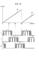
- the angle detection output S ⁇ illustrated in Fig. 6 is supplied to a pulse-width modulation circuit (pulse control circuit) 50.
- the duty ratio of the motor driving power supplied from a power supply circuit 49 is changed by the pulse-width modulation circuit 50, and the motor driving power is supplied to the driving circuit 46.
- the pulse-width modulation circuit 50 detects angle change (time change) in the supply period for the phase-U driving power by referring to the angle detection output S ⁇ . Power is adjusted so that the driving power is decreased at the beginning of the phase-U supply period, is then increased, and is further decreased. This driving power is subjected to analog-digital conversion. As a result, through the switching performed by the division switching circuit 48, the phase-U driving power which is supplied from the driving circuit 46 to the motor coils 43 forms pulse group P power as illustrated in Fig. 10 . The duty ratio of the power supply becomes large at the middle of the supply period, and becomes small before and after the middle of the supply period. The pulse group P is generated in a similar manner in all of supply periods for the phase-U driving power. Similarly, the pulse-width modulation circuit 50 controls the duty ratio of the power supply in a supply period for the phase-V driving power and a supply period for the phase-W driving power.
- the phase-U driving power, the phase-V driving power, and the phase-W driving power are supplied to the motor coils 43, causing the rotor magnet 41 to rotate in the clockwise direction (CW).
- the phase-U driving power, the phase-V driving power, and the phase-W driving power which are switched to each other at every 120° are supplied in the form of a pulse group P.
- the substantial current amount gradually increases and gradually decreases. Therefore, ripples produced when the driving power for each of the phases is switched to another can be reduced.
- the angle detection output S ⁇ which is an analog output is supplied to the three-phase comparator 47, and a dividing signal is supplied to the division switching circuit 48, whereby the supply timings and the supply periods for the phase-U driving power, the phase-V driving power, and the phase-W driving power are determined as illustrated in Fig. 10 .
- the supply timings occur at every 120°, and the supply periods have a time width of 180°.
- a change in the absolute angle of the angle detection output S ⁇ (angle of inclination of the angle detection output S ⁇ illustrated in Fig. 6 ) is referred to, and the duty ratio of the driving power in the middle portion of the supply period is made different from those in the portions before and after the middle portion. This control achieves motor rotation having no ripples.
- the motor controller controls the driving power of each of the three phases by using the angle detection output S ⁇ which has analog values and which is generated from the detected outputs from the magnetoresistive effect devices. Therefore, even when the rotation shaft 6 rotates at high rotational speed, the motor controller can control the rotation at a speed in line with the high-speed rotation.
Landscapes
- Engineering & Computer Science (AREA)
- Power Engineering (AREA)
- Physics & Mathematics (AREA)
- Condensed Matter Physics & Semiconductors (AREA)
- General Physics & Mathematics (AREA)
- Control Of Motors That Do Not Use Commutators (AREA)
- Transmission And Conversion Of Sensor Element Output (AREA)
- Measurement Of Length, Angles, Or The Like Using Electric Or Magnetic Means (AREA)
Description
- The present invention relates to a motor controller which controls three-phase driving power by using an analog output which is analogous to a linear function that is proportional to the rotation angle of a rotation shaft.
- In motor controllers which control a three-phase motor, three-phase driving power for the phase U, the phase V, and the phase W is supplied to motor coils in accordance with the rotation phase of a motor.
- In a motor controller described in
WO2012/102113 A1 , an arithmetic processing unit calculates a motor control signal, and a logic circuit supplied with the motor control signal calculates a driving signal for each of the phases of the three-phase motor. A pre-driver circuit is controlled on the basis of the driving signal, and the three-phase motor is controlled. - The motor controller described in
WO2012/102113 A1 generates a driving signal for driving the three-phase motor, through digital calculation, resulting in a complicated circuit configuration. In addition, the digital calculation takes time. Accordingly, when the motor rotates at high speed, there arises a problem in that the digital calculation fails to be performed at a speed in line with the rotational speed. - The present invention provides a motor controller which enables three-phase driving power to be switched by using an analog output obtained by using a simple circuit configuration, and which enables the switching to be performed at a speed in line with high-speed rotation.
- According to an aspect, there is provided a motor controller including a motor driver and an angle detection device. The motor driver supplies three-phase driving power to a motor coil. The angle detection device detects a rotation angle of a rotation shaft. The angle detection device includes a rotating magnetic field, a first magnetic detector, a second magnetic detector, and an analog mixer. The rotating magnetic field is formed in accordance with the rotation of the rotation shaft. The first magnetic detector obtains a detected output analogous to a sine wave which is a rotation angle function for the rotating magnetic field. The second magnetic detector obtains a detected output analogous to a cosine wave. The analog mixer forms an angle detection output analogous to a linear function from the detected output analogous to the sine wave and from the detected output analogous to the cosine wave. The angle detection output is analog. The motor driver includes a division detecting unit and a driving circuit. The division detecting unit detects a 120° rotation angle of the rotation shaft from the angle detection output. The driving circuit supplies the three-phase driving power to the motor coil in accordance with a timing at which the division detecting unit detects a dividing signal at every 120°.
- The motor controller provided by the present invention uses the angle detection output which is analog and which is obtained on the basis of the detected outputs from the first magnetic detector and the second magnetic detector, or uses the angle detection output which is analog and which is obtained through gain adjustment so as to switch the three-phase driving power at every 120° of rotation of the rotation shaft. Therefore, the circuit configuration is simple. Even when the rotational speed of the rotation shaft is high, the three-phase driving power can be generated at a speed in line with the rotational speed.
- Preferably, in the motor controller in the present invention, the motor driver further includes a pulse control circuit that changes a duty ratio of the three-phase driving power on the basis of the angle detection output.
- By changing the duty ratio of the three-phase driving power, upon switching to any of the phases, ripples in the rotation driving torque may be decreased. In addition, the angle detection output which is analog is used to directly control the three-phase power, making the circuit configuration simple and enabling the rotation shaft to rotate smoothly.
- Preferably, in the angle detection device in the present invention, the analog mixer includes a switching circuit and a bias adding circuit. The switching circuit cuts out detected output portions analogous to a linear function from the detected outputs obtained from the first magnetic detector and the second magnetic detector. The detected outputs is analog. The bias adding circuit connects the detected output portions to each other by supplying bias power to any of the detected output portions, so as to use the result as the angle detection output.
- By providing the switching circuit and the bias adding circuit, the angle detection output which is analog and which is continuous in the angle range of 360° can be generated.
- Preferably, in the angle detection device in the present invention, the angle detection device further includes first output circuits, second output circuits, and comparators. The first output circuits obtain a first detected output and a second detected output from the first magnetic detector. The second detected output is an output whose positive-negative polarity is opposite to a polarity of the first detected output. The second output circuits obtain a third detected output and a fourth detected output from the second magnetic detector. The fourth detected output is an output whose positive-negative polarity is opposite to a polarity of the third detected output. The comparators compare any of the first, second, third, and fourth detected outputs with another. A timing at which the switching circuit performs switching is determined on the basis of the comparison results from the comparators.
- For example, the switching circuit allows each of the first, second, third, and fourth detected outputs to be cut out in a corresponding period of 90°, whereby the detected output portions are obtained. In this case, each of the first, second, third, and fourth detected outputs is cut out in a range from -45° to +45° with respect to the midpoint of the amplitude.
- Preferably, in the angle detection device in the present invention, each of the first magnetic detector and the second magnetic detector includes a bridge circuit including magnetoresistive effect devices. A direction of a sensing axis of a first magnetoresistive effect device included in the first magnetic detector is orthogonal to a direction of a sensing axis of a second magnetoresistive effect device included in the second magnetic detector.
- In the motor controller provided by the present invention, the angle detection output which is analog is generated. By using the angle detection output, timings corresponding to intervals of 120° are obtained to switch the three-phase driving power. Therefore, the circuit configuration may be simple. Complicated calculation is not necessary. Therefore, even when the rotational speed of the rotation shaft is high, the angle detection output may be obtained at a speed in line with the rotational speed of the rotation shaft, enabling the three-phase driving power to be controlled with high accuracy.
-
-
Fig. 1 is an external view of a motor controller according to an embodiment of the present invention; -
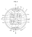
Fig. 2 is a plan view of the configuration of a rotation detection unit included in the motor controller; -
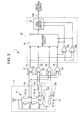
Fig. 3 is a circuit block diagram illustrating the circuit configuration of an angle detection device; -
Fig. 4 is a diagram illustrating four types of detected output obtained from first and second magnetic detectors; -
Fig. 5 is a diagram illustrating detected output portions obtained by cutting the detected outputs obtained from the first and second magnetic detectors; -
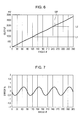
Fig. 6 is a diagram illustrating an angle detection output in which the detected output portions are connected to each other; -
Fig. 7 is a diagram illustrating distribution of error occurring between the angle detection output illustrated inFig. 6 and a linear function; -
Fig. 8 is a diagram for describing a rotation driving unit of a three-phase motor; -
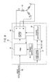
Fig. 9 is a diagram illustrating the circuit configuration of a motor driver; and -
Fig. 10 is a diagram illustrating an angle detection output and three-phase driving power. - A
motor controller 5 illustrated inFig. 1 includes arotation shaft 6, arotation driving unit 7 which drives therotation shaft 6, and arotation detection unit 8 which detects rotation of therotation shaft 6. - As illustrated in
Fig. 8 , therotation driving unit 7 constitutes a driving unit of a brushless motor, and includes arotor magnet 41 which rotates with therotation shaft 6. Three-phase stator yokes 42 are disposed inside therotor magnet 41 at angular intervals of 120° in the rotation direction, and each of thestator yokes 42 is connected to a corresponding one ofmotor coils 43 for the phase U, the phase V, and the phase W. - The
rotation detection unit 8 constitutes a part of anangle detection device 1. An angle detection output obtained from theangle detection device 1 controls amotor driver 45, and three-phase driving power is supplied from themotor driver 45 to themotor coils 43. - As illustrated in
Fig. 2 , therotation detection unit 8 included in themotor controller 5 includes arotor 2 which rotates with therotation shaft 6 of the motor. Adetection substrate 3 is fixed on the stator side inside therotor 2. - Two magnets M1 and M2 are fixed at angular intervals of 180° in the
rotor 2. The north pole of the magnet M1 faces the magnet M2, and the south pole of the magnet M2 faces the magnet M1. A magnetic field H is formed in the direction from the magnet M1 to the magnet M2. - The
rotor 2 rotates in the clockwise direction (CW) with therotation shaft 6 of the motor. As a result, a rotating magnetic field in which the magnetic field H rotates in the clockwise direction is formed inside therotor 2. - First magnetoresistive effect devices R(+s) and R(-s) and second magnetoresistive effect devices R(+c) and R(-c) are mounted as magnetic detection devices on the
detection substrate 3. InFig. 2 , thedetection substrate 3 and the magnetoresistive effect devices are illustrated as large components, but theactual detection substrate 3 and the actual magnetoresistive effect devices have extremely small dimensions compared with the diameter of the rotation path of the magnets M1 and M2. During rotation of therotor 2, to each of the magnetoresistive effect devices on thedetection substrate 3, a rotating magnetic field in the same direction is applied. - Alternatively, the magnets M1 and M2 may be fixed on the stator side, and the
detection substrate 3 may rotate with therotation shaft 6. - The sensing axis P of the first magnetoresistive effect devices R(+s) and R(-s) is orthogonal to that of the second magnetoresistive effect devices R(+c) and R(-c). Two types of first magnetoresistive effect devices are provided: the R(+s) whose sensing axis P goes in the X2 direction, and the R(-s) whose sensing axis P goes in the X1 direction. Two types of second magnetoresistive effect devices are provided: the R(+c) whose sensing axis P goes in the Y2 direction, and the R(-c) whose sensing axis P goes in the Y1 direction.
- Each of the magnetoresistive effect devices is a giant magnetoresistive (GMR) device using a giant magnetoresistance effect, a tunneling magnetoresistive (TMR) device using a tunnel effect, or an anisotropic magnetoresistive (AMR) device.
- As illustrated in
Fig. 2 , a magnetoresistive effect device includeselectrode portions 4 and anelement portion 5 disposed between theelectrode portions 4. Theelement portion 5 is formed in a meander pattern in the X-Y plane, and has a multilayer structure of pinned magnetic layer/nonmagnetic layer/free magnetic layer. The pinned magnetization direction of the pinned magnetic layer matches the sensing axis P. The magnetization direction of the free magnetic layer is changed in accordance with the direction of the external magnetic field H. - The electric resistance of the magnetoresistive effect device is changed in accordance with a relative angle of the pinned magnetization direction relative to the magnetization direction of the free magnetic layer. When the external magnetic field H is applied in the sensing axis P direction, the electric resistance value of the magnetoresistive effect device is the minimum value. When the external magnetic field H is applied in the direction opposite to the sensing axis P, the electric resistance value is the maximum value. When the external magnetic field H is applied in the direction orthogonal to the sensing axis P, the electric resistance value of the magnetoresistive effect device is the midpoint value.
- The magnetization direction of the pinned magnetic layer is fixed by subjecting a multilayer structure including the pinned magnetic layer and the antiferromagnetic layer to heat treatment in a magnetic field. Alternatively, the pinned magnetic layer may have a synthetic ferrimagnetic structure of magnetic layer/non-magnetic intermediate layer/magnetic layer, which is self-pinned so that magnetization of the magnetic layers is fixed in an anti-parallel manner. In this case, the magnetization is fixed by forming one of the magnetic layers in a magnetic field.
- As illustrated in
Fig. 3 , in theangle detection device 1, a firstmagnetic detector 11 and a secondmagnetic detector 12 are formed on thedetection substrate 3. - The first
magnetic detector 11 is a full-bridge circuit including the first magnetoresistive effect devices R(+s) and R(-s) in which the direction of the sensing axis P of the first magnetoresistive effect devices R(+s) is opposite to that of the first magnetoresistive effect devices R(-s). The secondmagnetic detector 12 is a full-bridge circuit including the second magnetoresistive effect devices R(+c) and R(-c) in which the direction of the sensing axis P of the second magnetoresistive effect devices R(+c) is opposite to that of the second magnetoresistive effect devices R(-c). - As illustrated in
Fig. 3 , midpoint outputs (midpoint output voltages) 11a and 11b from the full-bridge circuit of the firstmagnetic detector 11 are supplied to afirst output circuit 21 and asecond output circuit 22. Thefirst output circuit 21 is a differential amplifier having a (+) input unit connected to themidpoint output 11a and a (-) input unit connected to themidpoint output 11b. Thesecond output circuit 22 is also a differential amplifier having a (+) input unit connected to themidpoint output 11b and a (-) input unit connected to themidpoint output 11a. - Midpoint outputs (midpoint output voltages) 12a and 12b from the full-bridge circuit of the second
magnetic detector 12 are supplied to athird output circuit 23 and afourth output circuit 24. Thethird output circuit 23 is a differential amplifier having a (+) input unit connected to themidpoint output 12a and a (-) input unit connected to themidpoint output 12b. Thefourth output circuit 24 is also a differential amplifier having a (+) input unit connected to themidpoint output 12b and a (-) input unit connected to themidpoint output 12a. - When the
rotor 2 illustrated inFig. 2 rotates in the clockwise direction (CW), a first detected output S1 is obtained from thefirst output circuit 21, and a second detected output S2 is obtained from thesecond output circuit 22. A third detected output S3 is obtained from thethird output circuit 23, and a fourth detected output S4 is obtained from thefourth output circuit 24. -
Fig. 4 illustrates the output waveforms of the first to fourth detected outputs S1 to S4. The horizontal axis represents a rotation angle (θ), and the vertical axis represents output intensity (voltage). - The polarity (positive or negative voltage) of the first detected output S1 is opposite to that of the second detected output S2. The polarity of the third detected output S3 is opposite to that of the fourth detected output S4. The phase of the first detected output S1 is different from that of the third detected output S3 by 90°, and the phase of the second detected output S2 is also different from that of the fourth detected output S4 by 90°. One of the first detected output S1 and the third detected output S3 is an output which changes in a manner analogous to a trigonometric function wave which is a sine wave, and the other is an output which changes in a manner analogous to a trigonometric function wave which is a cosine wave.
- The horizontal axis in
Fig. 4 represents the rotation angle θ of therotor 2. In this representation of the rotation angle θ, the origin (0°) represents the state in which the center of the width of the magnet M1 illustrated inFig. 2 is positioned on the reference line Z.Fig. 2 illustrates the state in which the magnet M1 of therotor 2 which is rotating has moved from the origin (reference axis Z) by 45° in the clockwise direction (CW). The output intensities of the first to fourth detected outputs S1 to S4 at that time are the output intensities plotted at the 45° mark on the horizontal axis inFig. 4 . At the 45° mark on the horizontal axis, the output intensity of the first detected output S1 and that of the second detected output S2 have the midpoint value; the output intensity of the third detected output S3 has the maximum value; and the output intensity of the fourth detected output S4 has the minimum value. - The amplitudes and the absolute values of the intensities of the output waveforms of the first to fourth detected outputs S1 to S4 illustrated in
Fig. 4 depend on the power supply voltage Vdd, gains which are set for theoutput circuits magnetic detector 11 and the secondmagnetic detector 12 which detect the rotating magnetic field are reflected as they are. - As illustrated in
Fig. 3 , the first to fourth detected outputs S1 to S4 are supplied to ananalog mixer 30. Theanalog mixer 30 includes a switchingcircuit 31,comparators - The
first comparator 32a compares the magnitudes of the intensities of the first detected output S1 and the fourth detected output S4 with each other, and the result is supplied to the switchingcircuit 31. Thesecond comparator 32b compares the magnitudes of the intensities of the first detected output S1 and the third detected output S3 with each other, and the result is supplied to the switchingcircuit 31. - The switching
circuit 31 performs a switching operation on the basis of the comparison results from thecomparators - Table 1 describes the comparison result from the
first comparator 32a, the comparison result from thesecond comparator 32b, and the detected output to be cut by the switchingcircuit 31 on the basis of these comparison results.Table 1 First comparator 32aSecond comparator 32bSwitching output (Detected output portion) Bias voltage S1 > S4 S1 < S3 S1 (S1c) +350 mV S1 > S4 S1 > S3 S4 (S4c) +1050 mV S1 < S4 S1 > S3 S2 (S2c) +1750 mV S1 < S4 S1 < S3 S3 (S3c) +2450 mV -
Fig. 5 illustrates detected output portions S1c, S4c, S2c, and S3c obtained through the cutting operation performed in the switching operation performed by the switchingcircuit 31. - As shown in Table 1, each of the
first comparator 32a and thesecond comparator 32b compares two detected outputs with each other, and the switchingcircuit 31 performs the switching operation, whereby, as illustrated inFig. 5 , in the 360° rotation of therotor 2 in the clockwise direction, four detected outputs are cut out at intervals of 90°. - In the range of the angle θ from 0° to 90°, as shown in the first row in Table 1, the first detected output S1 in the range from -45° to + 45° with respect to the midpoint of its amplitude (voltage width) is cut out to obtain the detected output portion S1c illustrated in
Fig. 5 . In the range of the angle θ from 90° to 180°, as shown in the second row in Table 1, the detected output S4 in the range from -45° to + 45° with respect to the midpoint of its amplitude (voltage width) is cut out to obtain the detected output portion S4c illustrated inFig. 5 . Similarly, in the range of the angle θ from 180° to 270°, the detected output portion S2c is obtained. In the range of the angle θ from 270° to 360°, the detected output portion S3c is obtained. - Since each of the detected output portions S1c, S4c, S2c, and S3c is cut out in the range from -45° to + 45° with respect to the midpoint of the amplitude from a corresponding one of the detected outputs which is analogous to a sine wave or a cosine wave, change in the output intensity approximately accords with a linear function.
- The
first comparator 32a and thesecond comparator 32b generate a signal for dividing the detected outputs at every 90° so that the detected output portions illustrated inFig. 5 are obtained. As long as the detected output portions illustrated inFig. 5 are obtained, the detected outputs to be compared with each other are not limited to the example shown in Table 1. - For example, even if the comparison condition is that S3 > S1 and S3 > S2, the first detected output S1 in the range of angle θ from 0° to 90° may be cut out, and the detected output portion S1c may be obtained.
- The detected output portions S1c, S4c, S2c, and S3c which are cut out by the switching
circuit 31 are supplied to the bias adding circuit 33. In the bias adding circuit 33, each of the detected output portions S1c, S4c, S2c, and S3c is supplied with a positive or negative bias voltage so that, as illustrated inFig. 6 , an angle detection output Sθ which is obtained by connecting the detected output portions S1c, S4c, S2c, and S3c to each other and which is analogous to a linear function is obtained. In the rightmost column in Table 1 illustrated above, bias voltage values supplied to the detected output portions S1c, S4c, S2c, and S3c in order to obtain the angle detection output illustrated inFig. 6 are shown as numeric values. - The bias adding circuit is constituted by, for example, a resistor and a variable resistor. A bias voltage is applied to the detected output portion S4c in
Fig. 5 so that the starting point of the detected output portion S4c is connected to the endpoint of the detected output portion S1c. Similarly, each of the detected output portions S2c and S3c is supplied with a bias voltage. By supplying the detected output portion S1c, which is first obtained, with a positive or negative bias voltage, as illustrated inFig. 6 , the starting point of the output obtained when the angle θ is 0° may match the zero point of the output voltage. - A change in the angle detection output Sθ illustrated in
Fig. 6 is analogous to a linear function.Fig. 7 illustrates intensity error occurring between the angle detection output illustrated inFig. 6 and the linear function. The error in the angle detection output Sθ with respect to the linear function approximately ranges from -0.5% to +0.5%. - The
angle detection device 1 according to the embodiment of the present invention uses an analog output obtained from the firstmagnetic detector 11 and the secondmagnetic detector 12 as they are or uses an analog output obtained through gain adjustment, whereby an angle detection output Sθ which is analogous to a linear function can be instantaneously obtained. Therefore, even when therotor 2 which is directly coupled to the motor is rotating, a rotation angle can be accurately detected. - In the
angle detection device 1 illustrated inFigs. 2 and3 , the firstmagnetic detector 11 is a full-bridge circuit including the first magnetoresistive effect devices R(+s) and R(-s), and the secondmagnetic detector 12 is a full-bridge circuit including the second magnetoresistive effect devices R(+c) and R(-c). - Alternatively, in the present invention, the first
magnetic detector 11 may be a full-bridge circuit obtained by combining either type of the R(+s) and the R(-s) as the first magnetoresistive effect devices with fixed resistors, or may be a half-bridge circuit using either type of the R(+s) and the R(-s). The same holds true for the secondmagnetic detector 12. - In the
analog mixer 30 illustrated inFig. 3 , the detected output portions which are cut out by the switchingcircuit 31 are supplied with bias power. Alternatively, the first to fourth detected outputs S1 to S4 which have been output from the first tofourth output circuits circuit 31 then cuts out the detected output portions, enabling an angle detection output Sθ which is continuous to be obtained from the switchingcircuit 31. - As illustrated in
Fig. 9 , themotor driver 45 includes a drivingcircuit 46, and three-phase driving power is supplied from the drivingcircuit 46 to the motor coils 43. - The
motor driver 45 includes a three-phase comparator 47, and the angle detection output Sθ generated in theangle detection device 1 illustrated inFig. 3 is supplied to the three-phase comparator 47. The three-phase comparator 47 functions as a division detecting unit, and compares the angle detection output Sθ with two thresholds L1 and L2 illustrated inFig. 6 . The threshold L1 is a voltage corresponding to the output intensity of the angle detection output Sθ obtained when the rotation angle θ of therotation shaft 6 and therotor 2reaches 120°. The threshold L2 is a voltage corresponding to the output intensity of the angle detection output Sθ obtained when the rotation angle θ of therotation shaft 6 and therotor 2reaches 240°. - A dividing signal is supplied from the three-
phase comparator 47 to thedivision switching circuit 48. When the intensity of the angle detection output Sθ which is output from theangle detection device 1 is equal to zero, a dividing signal Sd0 is supplied from the three-phase comparator 47 to thedivision switching circuit 48; when the angle detection output Sθ matches the threshold L1, a dividing signal Sd1 is supplied; and when the intensity of the angle detection output Sθ matches the threshold L2, a dividing signal Sd2 is supplied. - When the dividing signal Sd0, Sd1, or Sd2 is supplied to the
division switching circuit 48, thedivision switching circuit 48 causes the supply timing of driving power supplied from the drivingcircuit 46 to the motor coils 43 to be switched. As illustrated inFig. 10 , when the dividing signal Sd0 is supplied from the three-phase comparator 47 to thedivision switching circuit 48, the drivingcircuit 46 sets a supply period which has a time width of 180° and in which phase-U driving power is supplied, for the motor coils 43. When the dividing signal Sd1 is supplied, a supply period which has a time width of 180° and in which phase-V driving power is supplied is set for the motor coils 43. When the dividing signal Sd2 is supplied, a supply period which has a time width of 180° and in which phase-W driving power is supplied is set for the motor coils 43. - In the
motor driver 45 illustrated inFig. 9 , the angle detection output Sθ illustrated inFig. 6 is supplied to a pulse-width modulation circuit (pulse control circuit) 50. The duty ratio of the motor driving power supplied from apower supply circuit 49 is changed by the pulse-width modulation circuit 50, and the motor driving power is supplied to the drivingcircuit 46. - The pulse-
width modulation circuit 50 detects angle change (time change) in the supply period for the phase-U driving power by referring to the angle detection output Sθ. Power is adjusted so that the driving power is decreased at the beginning of the phase-U supply period, is then increased, and is further decreased. This driving power is subjected to analog-digital conversion. As a result, through the switching performed by thedivision switching circuit 48, the phase-U driving power which is supplied from the drivingcircuit 46 to the motor coils 43 forms pulse group P power as illustrated inFig. 10 . The duty ratio of the power supply becomes large at the middle of the supply period, and becomes small before and after the middle of the supply period. The pulse group P is generated in a similar manner in all of supply periods for the phase-U driving power. Similarly, the pulse-width modulation circuit 50 controls the duty ratio of the power supply in a supply period for the phase-V driving power and a supply period for the phase-W driving power. - The phase-U driving power, the phase-V driving power, and the phase-W driving power are supplied to the motor coils 43, causing the
rotor magnet 41 to rotate in the clockwise direction (CW). The phase-U driving power, the phase-V driving power, and the phase-W driving power which are switched to each other at every 120° are supplied in the form of a pulse group P. In a supply period for each type of driving power, the substantial current amount gradually increases and gradually decreases. Therefore, ripples produced when the driving power for each of the phases is switched to another can be reduced. - In the
motor controller 5, the angle detection output Sθ which is an analog output is supplied to the three-phase comparator 47, and a dividing signal is supplied to thedivision switching circuit 48, whereby the supply timings and the supply periods for the phase-U driving power, the phase-V driving power, and the phase-W driving power are determined as illustrated inFig. 10 . The supply timings occur at every 120°, and the supply periods have a time width of 180°. In a supply period for the driving power of each phase, a change in the absolute angle of the angle detection output Sθ (angle of inclination of the angle detection output Sθ illustrated inFig. 6 ) is referred to, and the duty ratio of the driving power in the middle portion of the supply period is made different from those in the portions before and after the middle portion. This control achieves motor rotation having no ripples. - The motor controller controls the driving power of each of the three phases by using the angle detection output Sθ which has analog values and which is generated from the detected outputs from the magnetoresistive effect devices. Therefore, even when the
rotation shaft 6 rotates at high rotational speed, the motor controller can control the rotation at a speed in line with the high-speed rotation.
Claims (7)
- A motor controller (5) comprising:a motor driver (45) that supplies three-phase driving power to a motor coil (43); andan angle detection device (1) that detects a rotation angle of a rotation shaft (6),wherein the angle detection device (1) includes
a rotating magnetic field that is formed in accordance with the rotation of the rotation shaft (6),
a first magnetic detector (11) that obtains a detected output analogous to a sine wave which is a rotation angle function for the rotating magnetic field,
a second magnetic detector (12) that obtains a detected output analogous to a cosine wave, and
an analog mixer (30) that forms an angle detection output (Sθ) analogous to a linear function from the detected output analogous to the sine wave and from the detected output analogous to the cosine wave, the angle detection output (Sθ) being analog, andwherein the motor driver (45) includes
a division detecting unit (47) that detects a 120° rotation angle of the rotation shaft (6) from the angle detection output (Sθ), and
a driving circuit (46) that supplies the three-phase driving power to the motor coil (43) in accordance with a timing at which the division detecting unit (47) detects a dividing signal at every 120°. - The motor controller (5) according to Claim 1, wherein the motor driver (45) further includes
a pulse control circuit (50) that changes a duty ratio of the three-phase driving power on the basis of the angle detection output (Sθ). - The angle detection device (1) according to Claim 1 or 2,
wherein the analog mixer (30) includes
a switching circuit (31) that cuts out a plurality of detected output portions analogous to a linear function from the detected outputs obtained from the first magnetic detector (11) and the second magnetic detector (12), the detected outputs being analog, and
a bias adding circuit (33) that connects the plurality of detected output portions to each other by supplying bias power to any of the plurality of detected output portions, so as to use the result as the angle detection output (Sθ). - The angle detection device (1) according to Claim 3, further comprising:output circuits (21, 22) that obtain a first detected output (S1) and a second detected output (S2) from the first magnetic detector (11), the second detected output (S2) being an output whose positive-negative polarity is opposite to a polarity of the first detected output (S1);output circuits (23, 24) that obtain a third detected output (S3) and a fourth detected output (S4) from the second magnetic detector (12), the fourth detected output (S4) being an output whose positive-negative polarity is opposite to a polarity of the third detected output (S3); andcomparators (32a, 32b) that compare any of the first, second, third, and fourth detected outputs with another,wherein a timing at which the switching circuit (31) performs switching is determined on the basis of the comparison results from the comparators (32a, 32b).
- The angle detection device (1) according to Claim 4, wherein the switching circuit (31) allows each of the first, second, third, and fourth detected outputs (S1, S2, S3, and S4) to be cut out in a 90° period so as to obtain the detected output portion (S1c, S2c, S3c, and S4c).
- The angle detection device (1) according to Claim 4 or 5,
wherein each of the first, second, third, and fourth detected outputs (S1, S2, S3, and S4) is cut out in a range from -45° to +45° with respect to the midpoint of an amplitude of the detected output (S1, S2, S3, and S4). - The angle detection device (1) according to one of Claims 1-6,
wherein each of the first magnetic detector (11) and the second magnetic detector (12) includes a bridge circuit including magnetoresistive effect devices, and
wherein a direction of a sensing axis of a first magnetoresistive effect device included in the first magnetic detector (11) is orthogonal to a direction of a sensing axis of a second magnetoresistive effect device included in the second magnetic detector (12).
Applications Claiming Priority (1)
| Application Number | Priority Date | Filing Date | Title |
|---|---|---|---|
| JP2013178568A JP2015049047A (en) | 2013-08-29 | 2013-08-29 | Motor controller |
Publications (3)
| Publication Number | Publication Date |
|---|---|
| EP2843825A2 true EP2843825A2 (en) | 2015-03-04 |
| EP2843825A3 EP2843825A3 (en) | 2016-01-20 |
| EP2843825B1 EP2843825B1 (en) | 2017-10-11 |
Family
ID=51392136
Family Applications (1)
| Application Number | Title | Priority Date | Filing Date |
|---|---|---|---|
| EP14182196.7A Active EP2843825B1 (en) | 2013-08-29 | 2014-08-26 | Motor controller |
Country Status (4)
| Country | Link |
|---|---|
| US (1) | US9337757B2 (en) |
| EP (1) | EP2843825B1 (en) |
| JP (1) | JP2015049047A (en) |
| CN (1) | CN104426438B (en) |
Cited By (1)
| Publication number | Priority date | Publication date | Assignee | Title |
|---|---|---|---|---|
| DE102024117622A1 (en) | 2023-06-30 | 2025-01-02 | Tdk Corporation | ANGLE DETECTION DEVICE, MOTOR DEVICE AND LOGIC SIGNAL GENERATOR |
Families Citing this family (7)
| Publication number | Priority date | Publication date | Assignee | Title |
|---|---|---|---|---|
| US9983274B2 (en) * | 2014-01-23 | 2018-05-29 | Mitsubishi Electric Corporation | Magnetic detection device |
| US10879820B2 (en) | 2017-06-12 | 2020-12-29 | Igarashi Electric Works Ltd. | Control device for brushless DC servo motor |
| JP6412281B1 (en) * | 2018-02-05 | 2018-10-24 | 株式会社 五十嵐電機製作所 | Brushless DC servo motor control device |
| JP7171380B2 (en) * | 2018-11-20 | 2022-11-15 | 日本電産サンキョー株式会社 | motor |
| CN111722156A (en) * | 2020-06-29 | 2020-09-29 | 深圳市优必选科技股份有限公司 | A detection circuit and detection method for positive and negative electrodes of a brushed motor, and a steering gear |
| US11733024B2 (en) | 2021-06-30 | 2023-08-22 | Allegro Microsystems, Llc | Use of channel information to generate redundant angle measurements on safety critical applications |
| US11624799B2 (en) * | 2021-07-20 | 2023-04-11 | Allegro Microsystems, Llc | Method and apparatus for detecting errors in a magnetic field sensor |
Citations (1)
| Publication number | Priority date | Publication date | Assignee | Title |
|---|---|---|---|---|
| WO2012102113A1 (en) | 2011-01-26 | 2012-08-02 | 日立オートモティブシステムズ株式会社 | Motor control device |
Family Cites Families (9)
| Publication number | Priority date | Publication date | Assignee | Title |
|---|---|---|---|---|
| US5859510A (en) * | 1993-02-17 | 1999-01-12 | Pitney Bowes Inc. | Commutation board for brushless motor |
| JP3491577B2 (en) * | 1999-10-27 | 2004-01-26 | 株式会社デンソー | Rotation angle detector |
| US6744230B2 (en) * | 2002-10-29 | 2004-06-01 | Honeywell International Inc. | Method and apparatus for fine resolution brushless motor control |
| GB2413905B (en) * | 2004-05-05 | 2006-05-03 | Imra Europ S A S Uk Res Ct | Permanent magnet synchronous motor and controller therefor |
| JP2006220530A (en) * | 2005-02-10 | 2006-08-24 | Matsushita Electric Ind Co Ltd | Absolute rotation angle detector |
| US7583080B2 (en) * | 2005-02-10 | 2009-09-01 | Panasonic Corporation | Rotation angle detection device and rotation angle correction method |
| US7714570B2 (en) * | 2006-06-21 | 2010-05-11 | Allegro Microsystems, Inc. | Methods and apparatus for an analog rotational sensor having magnetic sensor elements |
| JP4100442B2 (en) * | 2006-09-29 | 2008-06-11 | ダイキン工業株式会社 | Motor drive control device and motor drive control system |
| JP5866956B2 (en) * | 2011-10-17 | 2016-02-24 | 株式会社デンソー | Magnetic sensor |
-
2013
- 2013-08-29 JP JP2013178568A patent/JP2015049047A/en active Pending
-
2014
- 2014-07-08 US US14/325,800 patent/US9337757B2/en active Active
- 2014-08-26 EP EP14182196.7A patent/EP2843825B1/en active Active
- 2014-08-28 CN CN201410432781.1A patent/CN104426438B/en active Active
Patent Citations (1)
| Publication number | Priority date | Publication date | Assignee | Title |
|---|---|---|---|---|
| WO2012102113A1 (en) | 2011-01-26 | 2012-08-02 | 日立オートモティブシステムズ株式会社 | Motor control device |
Cited By (1)
| Publication number | Priority date | Publication date | Assignee | Title |
|---|---|---|---|---|
| DE102024117622A1 (en) | 2023-06-30 | 2025-01-02 | Tdk Corporation | ANGLE DETECTION DEVICE, MOTOR DEVICE AND LOGIC SIGNAL GENERATOR |
Also Published As
| Publication number | Publication date |
|---|---|
| CN104426438B (en) | 2017-04-12 |
| EP2843825B1 (en) | 2017-10-11 |
| EP2843825A3 (en) | 2016-01-20 |
| JP2015049047A (en) | 2015-03-16 |
| US20150061559A1 (en) | 2015-03-05 |
| US9337757B2 (en) | 2016-05-10 |
| CN104426438A (en) | 2015-03-18 |
Similar Documents
| Publication | Publication Date | Title |
|---|---|---|
| EP2843825B1 (en) | Motor controller | |
| JP5523571B2 (en) | Method for evaluating multiple signals from an angle sensor | |
| US10651767B2 (en) | Methods and apparatus for three-phase motor control with error compensation | |
| KR102042911B1 (en) | Power converter and motor drive | |
| US9438152B2 (en) | Electronically commutated electric motor comprising rotor position detection with interference field compensation | |
| JP6481254B2 (en) | Phase detection device, motor drive control device, and motor device | |
| US10871365B2 (en) | Angle detection device and electric power steering apparatus | |
| US10505482B2 (en) | Magnetic pole direction detection device | |
| WO2017058983A1 (en) | Linear hall effect sensors for multi-phase permanent magnet motors with pwm drive | |
| US11637482B2 (en) | Magnetic sensor system for motor control | |
| CN105915139A (en) | Vector control permanent magnet synchronous servo motor initial magnetic pole position search method | |
| JP2018009818A (en) | Motor equipment | |
| JP6398233B2 (en) | Phase detection device, motor drive control device, and motor device | |
| US9647586B2 (en) | Signal amplifier, phase detector, and motor drive controller | |
| EP2843372B1 (en) | Angle detection device | |
| US20150102754A1 (en) | Apparatus for driving motor and controlling method thereof | |
| US20220290968A1 (en) | Rotational angle sensor device and method for determining a rotational angle, and control device for an electric motor | |
| JP6796573B2 (en) | Magnetic pole direction detector | |
| JP2015061411A (en) | Linear/rotary actuator and method for controlling the same | |
| US20210044235A1 (en) | Method for determining the angular position of the rotor of an inverter-fed synchronous motor, and an apparatus for carrying out the method | |
| JP2009229314A (en) | Rotation angle detector | |
| JP5615892B2 (en) | Magnetization method and apparatus | |
| TWI889937B (en) | Motor control device | |
| JP4899410B2 (en) | Magnetic encoder device | |
| JP2008228529A (en) | Method and apparatus for driving control of permanent magnet synchronous motor |
Legal Events
| Date | Code | Title | Description |
|---|---|---|---|
| 17P | Request for examination filed |
Effective date: 20140826 |
|
| AK | Designated contracting states |
Kind code of ref document: A2 Designated state(s): AL AT BE BG CH CY CZ DE DK EE ES FI FR GB GR HR HU IE IS IT LI LT LU LV MC MK MT NL NO PL PT RO RS SE SI SK SM TR |
|
| AX | Request for extension of the european patent |
Extension state: BA ME |
|
| PUAI | Public reference made under article 153(3) epc to a published international application that has entered the european phase |
Free format text: ORIGINAL CODE: 0009012 |
|
| PUAL | Search report despatched |
Free format text: ORIGINAL CODE: 0009013 |
|
| AK | Designated contracting states |
Kind code of ref document: A3 Designated state(s): AL AT BE BG CH CY CZ DE DK EE ES FI FR GB GR HR HU IE IS IT LI LT LU LV MC MK MT NL NO PL PT RO RS SE SI SK SM TR |
|
| AX | Request for extension of the european patent |
Extension state: BA ME |
|
| RIC1 | Information provided on ipc code assigned before grant |
Ipc: H02P 6/12 20060101AFI20151211BHEP Ipc: G01R 33/09 20060101ALI20151211BHEP |
|
| R17P | Request for examination filed (corrected) |
Effective date: 20160621 |
|
| RBV | Designated contracting states (corrected) |
Designated state(s): AL AT BE BG CH CY CZ DE DK EE ES FI FR GB GR HR HU IE IS IT LI LT LU LV MC MK MT NL NO PL PT RO RS SE SI SK SM TR |
|
| GRAP | Despatch of communication of intention to grant a patent |
Free format text: ORIGINAL CODE: EPIDOSNIGR1 |
|
| RIC1 | Information provided on ipc code assigned before grant |
Ipc: H02P 6/12 20060101AFI20170412BHEP Ipc: G01R 33/09 20060101ALI20170412BHEP |
|
| INTG | Intention to grant announced |
Effective date: 20170511 |
|
| GRAS | Grant fee paid |
Free format text: ORIGINAL CODE: EPIDOSNIGR3 |
|
| GRAA | (expected) grant |
Free format text: ORIGINAL CODE: 0009210 |
|
| AK | Designated contracting states |
Kind code of ref document: B1 Designated state(s): AL AT BE BG CH CY CZ DE DK EE ES FI FR GB GR HR HU IE IS IT LI LT LU LV MC MK MT NL NO PL PT RO RS SE SI SK SM TR |
|
| REG | Reference to a national code |
Ref country code: GB Ref legal event code: FG4D |
|
| REG | Reference to a national code |
Ref country code: CH Ref legal event code: EP |
|
| REG | Reference to a national code |
Ref country code: IE Ref legal event code: FG4D |
|
| REG | Reference to a national code |
Ref country code: AT Ref legal event code: REF Ref document number: 936850 Country of ref document: AT Kind code of ref document: T Effective date: 20171115 |
|
| REG | Reference to a national code |
Ref country code: DE Ref legal event code: R096 Ref document number: 602014015621 Country of ref document: DE |
|
| REG | Reference to a national code |
Ref country code: NL Ref legal event code: MP Effective date: 20171011 |
|
| REG | Reference to a national code |
Ref country code: LT Ref legal event code: MG4D |
|
| REG | Reference to a national code |
Ref country code: AT Ref legal event code: MK05 Ref document number: 936850 Country of ref document: AT Kind code of ref document: T Effective date: 20171011 |
|
| PG25 | Lapsed in a contracting state [announced via postgrant information from national office to epo] |
Ref country code: NL Free format text: LAPSE BECAUSE OF FAILURE TO SUBMIT A TRANSLATION OF THE DESCRIPTION OR TO PAY THE FEE WITHIN THE PRESCRIBED TIME-LIMIT Effective date: 20171011 |
|
| PG25 | Lapsed in a contracting state [announced via postgrant information from national office to epo] |
Ref country code: NO Free format text: LAPSE BECAUSE OF FAILURE TO SUBMIT A TRANSLATION OF THE DESCRIPTION OR TO PAY THE FEE WITHIN THE PRESCRIBED TIME-LIMIT Effective date: 20180111 Ref country code: LT Free format text: LAPSE BECAUSE OF FAILURE TO SUBMIT A TRANSLATION OF THE DESCRIPTION OR TO PAY THE FEE WITHIN THE PRESCRIBED TIME-LIMIT Effective date: 20171011 Ref country code: FI Free format text: LAPSE BECAUSE OF FAILURE TO SUBMIT A TRANSLATION OF THE DESCRIPTION OR TO PAY THE FEE WITHIN THE PRESCRIBED TIME-LIMIT Effective date: 20171011 Ref country code: ES Free format text: LAPSE BECAUSE OF FAILURE TO SUBMIT A TRANSLATION OF THE DESCRIPTION OR TO PAY THE FEE WITHIN THE PRESCRIBED TIME-LIMIT Effective date: 20171011 Ref country code: SE Free format text: LAPSE BECAUSE OF FAILURE TO SUBMIT A TRANSLATION OF THE DESCRIPTION OR TO PAY THE FEE WITHIN THE PRESCRIBED TIME-LIMIT Effective date: 20171011 |
|
| PG25 | Lapsed in a contracting state [announced via postgrant information from national office to epo] |
Ref country code: LV Free format text: LAPSE BECAUSE OF FAILURE TO SUBMIT A TRANSLATION OF THE DESCRIPTION OR TO PAY THE FEE WITHIN THE PRESCRIBED TIME-LIMIT Effective date: 20171011 Ref country code: AT Free format text: LAPSE BECAUSE OF FAILURE TO SUBMIT A TRANSLATION OF THE DESCRIPTION OR TO PAY THE FEE WITHIN THE PRESCRIBED TIME-LIMIT Effective date: 20171011 Ref country code: HR Free format text: LAPSE BECAUSE OF FAILURE TO SUBMIT A TRANSLATION OF THE DESCRIPTION OR TO PAY THE FEE WITHIN THE PRESCRIBED TIME-LIMIT Effective date: 20171011 Ref country code: BG Free format text: LAPSE BECAUSE OF FAILURE TO SUBMIT A TRANSLATION OF THE DESCRIPTION OR TO PAY THE FEE WITHIN THE PRESCRIBED TIME-LIMIT Effective date: 20180111 Ref country code: GR Free format text: LAPSE BECAUSE OF FAILURE TO SUBMIT A TRANSLATION OF THE DESCRIPTION OR TO PAY THE FEE WITHIN THE PRESCRIBED TIME-LIMIT Effective date: 20180112 Ref country code: RS Free format text: LAPSE BECAUSE OF FAILURE TO SUBMIT A TRANSLATION OF THE DESCRIPTION OR TO PAY THE FEE WITHIN THE PRESCRIBED TIME-LIMIT Effective date: 20171011 Ref country code: IS Free format text: LAPSE BECAUSE OF FAILURE TO SUBMIT A TRANSLATION OF THE DESCRIPTION OR TO PAY THE FEE WITHIN THE PRESCRIBED TIME-LIMIT Effective date: 20180211 |
|
| REG | Reference to a national code |
Ref country code: DE Ref legal event code: R097 Ref document number: 602014015621 Country of ref document: DE |
|
| PG25 | Lapsed in a contracting state [announced via postgrant information from national office to epo] |
Ref country code: CZ Free format text: LAPSE BECAUSE OF FAILURE TO SUBMIT A TRANSLATION OF THE DESCRIPTION OR TO PAY THE FEE WITHIN THE PRESCRIBED TIME-LIMIT Effective date: 20171011 Ref country code: SK Free format text: LAPSE BECAUSE OF FAILURE TO SUBMIT A TRANSLATION OF THE DESCRIPTION OR TO PAY THE FEE WITHIN THE PRESCRIBED TIME-LIMIT Effective date: 20171011 Ref country code: EE Free format text: LAPSE BECAUSE OF FAILURE TO SUBMIT A TRANSLATION OF THE DESCRIPTION OR TO PAY THE FEE WITHIN THE PRESCRIBED TIME-LIMIT Effective date: 20171011 Ref country code: DK Free format text: LAPSE BECAUSE OF FAILURE TO SUBMIT A TRANSLATION OF THE DESCRIPTION OR TO PAY THE FEE WITHIN THE PRESCRIBED TIME-LIMIT Effective date: 20171011 |
|
| PLBE | No opposition filed within time limit |
Free format text: ORIGINAL CODE: 0009261 |
|
| STAA | Information on the status of an ep patent application or granted ep patent |
Free format text: STATUS: NO OPPOSITION FILED WITHIN TIME LIMIT |
|
| REG | Reference to a national code |
Ref country code: FR Ref legal event code: PLFP Year of fee payment: 5 |
|
| PG25 | Lapsed in a contracting state [announced via postgrant information from national office to epo] |
Ref country code: RO Free format text: LAPSE BECAUSE OF FAILURE TO SUBMIT A TRANSLATION OF THE DESCRIPTION OR TO PAY THE FEE WITHIN THE PRESCRIBED TIME-LIMIT Effective date: 20171011 Ref country code: PL Free format text: LAPSE BECAUSE OF FAILURE TO SUBMIT A TRANSLATION OF THE DESCRIPTION OR TO PAY THE FEE WITHIN THE PRESCRIBED TIME-LIMIT Effective date: 20171011 Ref country code: SM Free format text: LAPSE BECAUSE OF FAILURE TO SUBMIT A TRANSLATION OF THE DESCRIPTION OR TO PAY THE FEE WITHIN THE PRESCRIBED TIME-LIMIT Effective date: 20171011 Ref country code: IT Free format text: LAPSE BECAUSE OF FAILURE TO SUBMIT A TRANSLATION OF THE DESCRIPTION OR TO PAY THE FEE WITHIN THE PRESCRIBED TIME-LIMIT Effective date: 20171011 |
|
| 26N | No opposition filed |
Effective date: 20180712 |
|
| PG25 | Lapsed in a contracting state [announced via postgrant information from national office to epo] |
Ref country code: SI Free format text: LAPSE BECAUSE OF FAILURE TO SUBMIT A TRANSLATION OF THE DESCRIPTION OR TO PAY THE FEE WITHIN THE PRESCRIBED TIME-LIMIT Effective date: 20171011 |
|
| REG | Reference to a national code |
Ref country code: DE Ref legal event code: R082 Ref document number: 602014015621 Country of ref document: DE Representative=s name: SCHMITT-NILSON SCHRAUD WAIBEL WOHLFROM PATENTA, DE Ref country code: DE Ref legal event code: R081 Ref document number: 602014015621 Country of ref document: DE Owner name: ALPS ALPINE CO., LTD., JP Free format text: FORMER OWNER: ALPS ELECTRIC CO., LTD., TOKYO, JP |
|
| PG25 | Lapsed in a contracting state [announced via postgrant information from national office to epo] |
Ref country code: MC Free format text: LAPSE BECAUSE OF FAILURE TO SUBMIT A TRANSLATION OF THE DESCRIPTION OR TO PAY THE FEE WITHIN THE PRESCRIBED TIME-LIMIT Effective date: 20171011 |
|
| REG | Reference to a national code |
Ref country code: CH Ref legal event code: PL |
|
| PG25 | Lapsed in a contracting state [announced via postgrant information from national office to epo] |
Ref country code: LU Free format text: LAPSE BECAUSE OF NON-PAYMENT OF DUE FEES Effective date: 20180826 Ref country code: CH Free format text: LAPSE BECAUSE OF NON-PAYMENT OF DUE FEES Effective date: 20180831 Ref country code: LI Free format text: LAPSE BECAUSE OF NON-PAYMENT OF DUE FEES Effective date: 20180831 |
|
| REG | Reference to a national code |
Ref country code: BE Ref legal event code: MM Effective date: 20180831 |
|
| PG25 | Lapsed in a contracting state [announced via postgrant information from national office to epo] |
Ref country code: BE Free format text: LAPSE BECAUSE OF NON-PAYMENT OF DUE FEES Effective date: 20180831 |
|
| PGFP | Annual fee paid to national office [announced via postgrant information from national office to epo] |
Ref country code: FR Payment date: 20190822 Year of fee payment: 6 |
|
| PGFP | Annual fee paid to national office [announced via postgrant information from national office to epo] |
Ref country code: GB Payment date: 20190821 Year of fee payment: 6 |
|
| PG25 | Lapsed in a contracting state [announced via postgrant information from national office to epo] |
Ref country code: MT Free format text: LAPSE BECAUSE OF NON-PAYMENT OF DUE FEES Effective date: 20180826 |
|
| PG25 | Lapsed in a contracting state [announced via postgrant information from national office to epo] |
Ref country code: TR Free format text: LAPSE BECAUSE OF FAILURE TO SUBMIT A TRANSLATION OF THE DESCRIPTION OR TO PAY THE FEE WITHIN THE PRESCRIBED TIME-LIMIT Effective date: 20171011 |
|
| PG25 | Lapsed in a contracting state [announced via postgrant information from national office to epo] |
Ref country code: PT Free format text: LAPSE BECAUSE OF FAILURE TO SUBMIT A TRANSLATION OF THE DESCRIPTION OR TO PAY THE FEE WITHIN THE PRESCRIBED TIME-LIMIT Effective date: 20171011 Ref country code: HU Free format text: LAPSE BECAUSE OF FAILURE TO SUBMIT A TRANSLATION OF THE DESCRIPTION OR TO PAY THE FEE WITHIN THE PRESCRIBED TIME-LIMIT; INVALID AB INITIO Effective date: 20140826 |
|
| PG25 | Lapsed in a contracting state [announced via postgrant information from national office to epo] |
Ref country code: IE Free format text: LAPSE BECAUSE OF NON-PAYMENT OF DUE FEES Effective date: 20180826 Ref country code: CY Free format text: LAPSE BECAUSE OF FAILURE TO SUBMIT A TRANSLATION OF THE DESCRIPTION OR TO PAY THE FEE WITHIN THE PRESCRIBED TIME-LIMIT Effective date: 20171011 Ref country code: MK Free format text: LAPSE BECAUSE OF NON-PAYMENT OF DUE FEES Effective date: 20171011 |
|
| PG25 | Lapsed in a contracting state [announced via postgrant information from national office to epo] |
Ref country code: AL Free format text: LAPSE BECAUSE OF FAILURE TO SUBMIT A TRANSLATION OF THE DESCRIPTION OR TO PAY THE FEE WITHIN THE PRESCRIBED TIME-LIMIT Effective date: 20171011 |
|
| GBPC | Gb: european patent ceased through non-payment of renewal fee |
Effective date: 20200826 |
|
| PG25 | Lapsed in a contracting state [announced via postgrant information from national office to epo] |
Ref country code: FR Free format text: LAPSE BECAUSE OF NON-PAYMENT OF DUE FEES Effective date: 20200831 |
|
| PG25 | Lapsed in a contracting state [announced via postgrant information from national office to epo] |
Ref country code: GB Free format text: LAPSE BECAUSE OF NON-PAYMENT OF DUE FEES Effective date: 20200826 |
|
| PGFP | Annual fee paid to national office [announced via postgrant information from national office to epo] |
Ref country code: DE Payment date: 20250820 Year of fee payment: 12 |