EP2843755A1 - Solar cell module and method for connecting same - Google Patents
Solar cell module and method for connecting same Download PDFInfo
- Publication number
- EP2843755A1 EP2843755A1 EP20130781625 EP13781625A EP2843755A1 EP 2843755 A1 EP2843755 A1 EP 2843755A1 EP 20130781625 EP20130781625 EP 20130781625 EP 13781625 A EP13781625 A EP 13781625A EP 2843755 A1 EP2843755 A1 EP 2843755A1
- Authority
- EP
- European Patent Office
- Prior art keywords
- solar cell
- conductive layer
- exposed portion
- conductive
- current collecting
- Prior art date
- Legal status (The legal status is an assumption and is not a legal conclusion. Google has not performed a legal analysis and makes no representation as to the accuracy of the status listed.)
- Withdrawn
Links
- 238000000034 method Methods 0.000 title claims description 21
- 238000010168 coupling process Methods 0.000 claims abstract description 29
- 238000009413 insulation Methods 0.000 claims abstract description 29
- 230000008878 coupling Effects 0.000 claims abstract description 26
- 238000005859 coupling reaction Methods 0.000 claims abstract description 26
- 239000000758 substrate Substances 0.000 claims description 88
- 238000004519 manufacturing process Methods 0.000 claims description 9
- 238000006243 chemical reaction Methods 0.000 abstract description 3
- 239000010410 layer Substances 0.000 description 117
- 239000000853 adhesive Substances 0.000 description 17
- 230000001070 adhesive effect Effects 0.000 description 17
- 239000011521 glass Substances 0.000 description 12
- 239000000463 material Substances 0.000 description 10
- 239000003054 catalyst Substances 0.000 description 8
- 239000003792 electrolyte Substances 0.000 description 8
- 230000003247 decreasing effect Effects 0.000 description 7
- BASFCYQUMIYNBI-UHFFFAOYSA-N platinum Chemical compound [Pt] BASFCYQUMIYNBI-UHFFFAOYSA-N 0.000 description 6
- -1 polyethylene terephthalate Polymers 0.000 description 6
- 239000011347 resin Substances 0.000 description 5
- 229920005989 resin Polymers 0.000 description 5
- 239000000565 sealant Substances 0.000 description 5
- 238000001723 curing Methods 0.000 description 4
- 239000011244 liquid electrolyte Substances 0.000 description 4
- 238000010248 power generation Methods 0.000 description 4
- 239000007784 solid electrolyte Substances 0.000 description 4
- 239000012790 adhesive layer Substances 0.000 description 3
- 239000000470 constituent Substances 0.000 description 3
- 238000005260 corrosion Methods 0.000 description 3
- 230000007797 corrosion Effects 0.000 description 3
- 230000007423 decrease Effects 0.000 description 3
- 239000011245 gel electrolyte Substances 0.000 description 3
- 239000007769 metal material Substances 0.000 description 3
- 229910044991 metal oxide Inorganic materials 0.000 description 3
- 239000002245 particle Substances 0.000 description 3
- 229910052697 platinum Inorganic materials 0.000 description 3
- 230000001235 sensitizing effect Effects 0.000 description 3
- 229910052709 silver Inorganic materials 0.000 description 3
- 239000004332 silver Substances 0.000 description 3
- 239000004925 Acrylic resin Substances 0.000 description 2
- XEEYBQQBJWHFJM-UHFFFAOYSA-N Iron Chemical compound [Fe] XEEYBQQBJWHFJM-UHFFFAOYSA-N 0.000 description 2
- 239000002390 adhesive tape Substances 0.000 description 2
- 229910052782 aluminium Inorganic materials 0.000 description 2
- XAGFODPZIPBFFR-UHFFFAOYSA-N aluminium Chemical compound [Al] XAGFODPZIPBFFR-UHFFFAOYSA-N 0.000 description 2
- 239000011231 conductive filler Substances 0.000 description 2
- 239000004020 conductor Substances 0.000 description 2
- 238000013007 heat curing Methods 0.000 description 2
- 150000002500 ions Chemical class 0.000 description 2
- 229910052751 metal Inorganic materials 0.000 description 2
- 239000002184 metal Substances 0.000 description 2
- 239000004065 semiconductor Substances 0.000 description 2
- 229920003002 synthetic resin Polymers 0.000 description 2
- 239000000057 synthetic resin Substances 0.000 description 2
- XOLBLPGZBRYERU-UHFFFAOYSA-N tin dioxide Chemical compound O=[Sn]=O XOLBLPGZBRYERU-UHFFFAOYSA-N 0.000 description 2
- 229910001887 tin oxide Inorganic materials 0.000 description 2
- 229920000178 Acrylic resin Polymers 0.000 description 1
- RYGMFSIKBFXOCR-UHFFFAOYSA-N Copper Chemical compound [Cu] RYGMFSIKBFXOCR-UHFFFAOYSA-N 0.000 description 1
- 239000004593 Epoxy Substances 0.000 description 1
- 239000004698 Polyethylene Substances 0.000 description 1
- 239000004743 Polypropylene Substances 0.000 description 1
- RTAQQCXQSZGOHL-UHFFFAOYSA-N Titanium Chemical compound [Ti] RTAQQCXQSZGOHL-UHFFFAOYSA-N 0.000 description 1
- 239000003522 acrylic cement Substances 0.000 description 1
- 238000005229 chemical vapour deposition Methods 0.000 description 1
- 229910052802 copper Inorganic materials 0.000 description 1
- 239000010949 copper Substances 0.000 description 1
- 125000004122 cyclic group Chemical group 0.000 description 1
- 230000000694 effects Effects 0.000 description 1
- 238000004070 electrodeposition Methods 0.000 description 1
- 239000003822 epoxy resin Substances 0.000 description 1
- 239000004744 fabric Substances 0.000 description 1
- 239000003349 gelling agent Substances 0.000 description 1
- PCHJSUWPFVWCPO-UHFFFAOYSA-N gold Chemical compound [Au] PCHJSUWPFVWCPO-UHFFFAOYSA-N 0.000 description 1
- 229910052737 gold Inorganic materials 0.000 description 1
- 239000010931 gold Substances 0.000 description 1
- 229910003437 indium oxide Inorganic materials 0.000 description 1
- PJXISJQVUVHSOJ-UHFFFAOYSA-N indium(iii) oxide Chemical compound [O-2].[O-2].[O-2].[In+3].[In+3] PJXISJQVUVHSOJ-UHFFFAOYSA-N 0.000 description 1
- 238000002347 injection Methods 0.000 description 1
- 239000007924 injection Substances 0.000 description 1
- 239000012774 insulation material Substances 0.000 description 1
- 238000007733 ion plating Methods 0.000 description 1
- 229910052742 iron Inorganic materials 0.000 description 1
- 239000007788 liquid Substances 0.000 description 1
- 150000002739 metals Chemical class 0.000 description 1
- 230000005012 migration Effects 0.000 description 1
- 238000013508 migration Methods 0.000 description 1
- 229920003207 poly(ethylene-2,6-naphthalate) Polymers 0.000 description 1
- 229920000767 polyaniline Polymers 0.000 description 1
- 229920001707 polybutylene terephthalate Polymers 0.000 description 1
- 229920005668 polycarbonate resin Polymers 0.000 description 1
- 239000004431 polycarbonate resin Substances 0.000 description 1
- 229920000647 polyepoxide Polymers 0.000 description 1
- 229920000728 polyester Polymers 0.000 description 1
- 229920006267 polyester film Polymers 0.000 description 1
- 229920000573 polyethylene Polymers 0.000 description 1
- 239000011112 polyethylene naphthalate Substances 0.000 description 1
- 229920000139 polyethylene terephthalate Polymers 0.000 description 1
- 239000005020 polyethylene terephthalate Substances 0.000 description 1
- 229920001721 polyimide Polymers 0.000 description 1
- 229920000193 polymethacrylate Polymers 0.000 description 1
- 229920000098 polyolefin Polymers 0.000 description 1
- 229920005672 polyolefin resin Polymers 0.000 description 1
- 229920001155 polypropylene Polymers 0.000 description 1
- 229920000128 polypyrrole Polymers 0.000 description 1
- 229920001343 polytetrafluoroethylene Polymers 0.000 description 1
- 239000004810 polytetrafluoroethylene Substances 0.000 description 1
- 229920000123 polythiophene Polymers 0.000 description 1
- 229920000915 polyvinyl chloride Polymers 0.000 description 1
- 239000004800 polyvinyl chloride Substances 0.000 description 1
- 239000013464 silicone adhesive Substances 0.000 description 1
- 239000000243 solution Substances 0.000 description 1
- 238000004544 sputter deposition Methods 0.000 description 1
- 229910052719 titanium Inorganic materials 0.000 description 1
- 239000010936 titanium Substances 0.000 description 1
- 239000005341 toughened glass Substances 0.000 description 1
- 238000001771 vacuum deposition Methods 0.000 description 1
Images


Classifications
-
- H—ELECTRICITY
- H01—ELECTRIC ELEMENTS
- H01G—CAPACITORS; CAPACITORS, RECTIFIERS, DETECTORS, SWITCHING DEVICES, LIGHT-SENSITIVE OR TEMPERATURE-SENSITIVE DEVICES OF THE ELECTROLYTIC TYPE
- H01G9/00—Electrolytic capacitors, rectifiers, detectors, switching devices, light-sensitive or temperature-sensitive devices; Processes of their manufacture
- H01G9/004—Details
- H01G9/04—Electrodes or formation of dielectric layers thereon
- H01G9/048—Electrodes or formation of dielectric layers thereon characterised by their structure
-
- H—ELECTRICITY
- H10—SEMICONDUCTOR DEVICES; ELECTRIC SOLID-STATE DEVICES NOT OTHERWISE PROVIDED FOR
- H10F—INORGANIC SEMICONDUCTOR DEVICES SENSITIVE TO INFRARED RADIATION, LIGHT, ELECTROMAGNETIC RADIATION OF SHORTER WAVELENGTH OR CORPUSCULAR RADIATION
- H10F19/00—Integrated devices, or assemblies of multiple devices, comprising at least one photovoltaic cell covered by group H10F10/00, e.g. photovoltaic modules
-
- H—ELECTRICITY
- H01—ELECTRIC ELEMENTS
- H01G—CAPACITORS; CAPACITORS, RECTIFIERS, DETECTORS, SWITCHING DEVICES, LIGHT-SENSITIVE OR TEMPERATURE-SENSITIVE DEVICES OF THE ELECTROLYTIC TYPE
- H01G9/00—Electrolytic capacitors, rectifiers, detectors, switching devices, light-sensitive or temperature-sensitive devices; Processes of their manufacture
- H01G9/20—Light-sensitive devices
- H01G9/2059—Light-sensitive devices comprising an organic dye as the active light absorbing material, e.g. adsorbed on an electrode or dissolved in solution
-
- H—ELECTRICITY
- H01—ELECTRIC ELEMENTS
- H01G—CAPACITORS; CAPACITORS, RECTIFIERS, DETECTORS, SWITCHING DEVICES, LIGHT-SENSITIVE OR TEMPERATURE-SENSITIVE DEVICES OF THE ELECTROLYTIC TYPE
- H01G9/00—Electrolytic capacitors, rectifiers, detectors, switching devices, light-sensitive or temperature-sensitive devices; Processes of their manufacture
- H01G9/20—Light-sensitive devices
- H01G9/2068—Panels or arrays of photoelectrochemical cells, e.g. photovoltaic modules based on photoelectrochemical cells
-
- H—ELECTRICITY
- H01—ELECTRIC ELEMENTS
- H01G—CAPACITORS; CAPACITORS, RECTIFIERS, DETECTORS, SWITCHING DEVICES, LIGHT-SENSITIVE OR TEMPERATURE-SENSITIVE DEVICES OF THE ELECTROLYTIC TYPE
- H01G9/00—Electrolytic capacitors, rectifiers, detectors, switching devices, light-sensitive or temperature-sensitive devices; Processes of their manufacture
- H01G9/20—Light-sensitive devices
- H01G9/2068—Panels or arrays of photoelectrochemical cells, e.g. photovoltaic modules based on photoelectrochemical cells
- H01G9/2081—Serial interconnection of cells
-
- H—ELECTRICITY
- H10—SEMICONDUCTOR DEVICES; ELECTRIC SOLID-STATE DEVICES NOT OTHERWISE PROVIDED FOR
- H10F—INORGANIC SEMICONDUCTOR DEVICES SENSITIVE TO INFRARED RADIATION, LIGHT, ELECTROMAGNETIC RADIATION OF SHORTER WAVELENGTH OR CORPUSCULAR RADIATION
- H10F19/00—Integrated devices, or assemblies of multiple devices, comprising at least one photovoltaic cell covered by group H10F10/00, e.g. photovoltaic modules
- H10F19/90—Structures for connecting between photovoltaic cells, e.g. interconnections or insulating spacers
-
- H—ELECTRICITY
- H01—ELECTRIC ELEMENTS
- H01G—CAPACITORS; CAPACITORS, RECTIFIERS, DETECTORS, SWITCHING DEVICES, LIGHT-SENSITIVE OR TEMPERATURE-SENSITIVE DEVICES OF THE ELECTROLYTIC TYPE
- H01G9/00—Electrolytic capacitors, rectifiers, detectors, switching devices, light-sensitive or temperature-sensitive devices; Processes of their manufacture
- H01G9/20—Light-sensitive devices
- H01G9/2027—Light-sensitive devices comprising an oxide semiconductor electrode
- H01G9/2031—Light-sensitive devices comprising an oxide semiconductor electrode comprising titanium oxide, e.g. TiO2
-
- H—ELECTRICITY
- H01—ELECTRIC ELEMENTS
- H01G—CAPACITORS; CAPACITORS, RECTIFIERS, DETECTORS, SWITCHING DEVICES, LIGHT-SENSITIVE OR TEMPERATURE-SENSITIVE DEVICES OF THE ELECTROLYTIC TYPE
- H01G9/00—Electrolytic capacitors, rectifiers, detectors, switching devices, light-sensitive or temperature-sensitive devices; Processes of their manufacture
- H01G9/20—Light-sensitive devices
- H01G9/2068—Panels or arrays of photoelectrochemical cells, e.g. photovoltaic modules based on photoelectrochemical cells
- H01G9/2077—Sealing arrangements, e.g. to prevent the leakage of the electrolyte
-
- Y—GENERAL TAGGING OF NEW TECHNOLOGICAL DEVELOPMENTS; GENERAL TAGGING OF CROSS-SECTIONAL TECHNOLOGIES SPANNING OVER SEVERAL SECTIONS OF THE IPC; TECHNICAL SUBJECTS COVERED BY FORMER USPC CROSS-REFERENCE ART COLLECTIONS [XRACs] AND DIGESTS
- Y02—TECHNOLOGIES OR APPLICATIONS FOR MITIGATION OR ADAPTATION AGAINST CLIMATE CHANGE
- Y02E—REDUCTION OF GREENHOUSE GAS [GHG] EMISSIONS, RELATED TO ENERGY GENERATION, TRANSMISSION OR DISTRIBUTION
- Y02E10/00—Energy generation through renewable energy sources
- Y02E10/50—Photovoltaic [PV] energy
-
- Y—GENERAL TAGGING OF NEW TECHNOLOGICAL DEVELOPMENTS; GENERAL TAGGING OF CROSS-SECTIONAL TECHNOLOGIES SPANNING OVER SEVERAL SECTIONS OF THE IPC; TECHNICAL SUBJECTS COVERED BY FORMER USPC CROSS-REFERENCE ART COLLECTIONS [XRACs] AND DIGESTS
- Y02—TECHNOLOGIES OR APPLICATIONS FOR MITIGATION OR ADAPTATION AGAINST CLIMATE CHANGE
- Y02E—REDUCTION OF GREENHOUSE GAS [GHG] EMISSIONS, RELATED TO ENERGY GENERATION, TRANSMISSION OR DISTRIBUTION
- Y02E10/00—Energy generation through renewable energy sources
- Y02E10/50—Photovoltaic [PV] energy
- Y02E10/542—Dye sensitized solar cells
-
- Y—GENERAL TAGGING OF NEW TECHNOLOGICAL DEVELOPMENTS; GENERAL TAGGING OF CROSS-SECTIONAL TECHNOLOGIES SPANNING OVER SEVERAL SECTIONS OF THE IPC; TECHNICAL SUBJECTS COVERED BY FORMER USPC CROSS-REFERENCE ART COLLECTIONS [XRACs] AND DIGESTS
- Y02—TECHNOLOGIES OR APPLICATIONS FOR MITIGATION OR ADAPTATION AGAINST CLIMATE CHANGE
- Y02P—CLIMATE CHANGE MITIGATION TECHNOLOGIES IN THE PRODUCTION OR PROCESSING OF GOODS
- Y02P70/00—Climate change mitigation technologies in the production process for final industrial or consumer products
- Y02P70/50—Manufacturing or production processes characterised by the final manufactured product
Definitions
- the present invention relates to a solar cell module and its coupling method, and particularly to a dye-sensitized solar cell module and its connecting method.
- FIG. 2 of Patent Document 1 a solar cell module is shown.
- the solar cell module of Patent Document 1 includes one solar cell having a conductive film exposed outside on a transparent substrate side, another solar cell having a conductive film exposed outside on a counter substrate side, and a conductive adhesive coupling the conductive films, which are stacked with each other in the vertical direction, to couple the solar cell module.
- the conductive adhesive is formed of a conductive filler and resinous principle at a certain ratio in order to balance the conductivity and the adhesiveness. If the ratio of the conductive filler in the conductive adhesive is increased, the electric resistance becomes lower. In contrast, if the ratio of the resinous principle is increased, the bonding strength is improved.
- Patent Document 1 Japanese Patent Publication 2007-265635
- the electric resistance between the solar cells might be increased due to the resinous principle in the conductive adhesive.
- the electric resistance of the conductive adhesive may change due to its thickness, if the thickness of the conductive adhesive are varied, it is assumed that the electric resistance may vary according to the solar cell modules.
- the coupling method using the conductive adhesive requires processes of pasting and curing the conductive adhesive, so that there are concerns over the possibility of increasing the number of the processes.
- the first invention is a solar cell module comprising at least two dye-sensitized solar cells coupled with each other.
- Each of the solar cells comprises:
- the solar cell module further comprises:
- the second invention is a solar cell module according to the structure of the first invention, wherein the first conductive layer includes a first conductive film, and a first current collecting line formed on a portion of the first conducive film where the photoelectrode layer is not formed, and the exposed portion of the first conductive layer is made of the first current collecting line.
- the third invention is a solar cell module according to the configuration of the first or the second invention, wherein the second conductive layer includes a second conductive film, and a second current collecting line formed on the second conductive layer, and the exposed portion of the second conductive layer is made of the second current collecting line.
- the fourth invention is a solar cell module according to the first or the second invention, wherein the second base member and the second conductive layer formed on the surface of the second base member are metallic plates.
- the counter electrode substrate is made of a metallic plate, it is possible to reduce the electric resistance of the counter electrode substrate.
- the configuration of the counter electrode substrate becomes simple.
- the fifth invention is a solar cell module according to any of the first through the fourth inventions, wherein the conductive member is a metallic plate or a metallic tape.
- the metallic plate or metallic tape so as to keep in contact with the exposed portion of the first conductive layer of the first solar cell and the exposed portion of the second conductive layer of the second solar cell is only required, the number of the processes is decreased. In addition, since the metallic plate or metallic tape is easy to obtain, the manufacturing cost decreases.
- the sixth invention is a solar cell module according to any of the first through the fourth inventions, wherein the coupling member is an insulation tape adhered so as to cover a connecting line between the substrates of the first solar cell and the second solar cell.
- the seventh invention is a method of manufacturing a solar cell module made of at least two dye-sensitized solar cell coupled with each other.
- Each of the solar cells comprises:
- the method comprises steps of:
- the conductive adhesive becomes unnecessary for coupling the solar cell module, the electric resistance between the solar cells is lowered.
- the processes of pasting and curing the conductive adhesive becomes unnecessary, the number of the processes is decreased.
- the electric resistance between the solar cells is lowered, thereby providing a solar cell module having excellent conversion efficiency.
- a solar cell module 10 is configured such that insulation tapes 53 are adhered to a first solar cell 20 and a second solar cell 20 so as to cover a connecting line between photoelectrode substrates 30 and a connecting line between counter electrode substrates 40.
- the solar cell 20 will be explained with reference to Fig. 2 and Fig. 3 .
- the solar cell 20 includes a photoelectrode substrate 30, a counter electrode substrate 40 facing the photoelectrode substrate 30, a charge conveyance layer 50 provided in an area through which the substrates 30, 40 face each other, and a sealant 51 located so as to seal the above-described area.
- the photoelectrode substrate 30 is a substrate constituting a light incident surface.
- the photoelectrode substrate 30 includes a first base member 31, a first conductive film 32, a photoelectrode layer 33 configured to pass a charge generated from the sensitized dye due to the light irradiation, and a first current collecting line 34 configured to efficiently collect electrons.
- the first conductive film 32 and the photoelectrode layer 33 are sequentially formed on one surface of the first base member 31.
- the first current collecting line 34 is formed on a portion of the first conductive film 32 where the photoelectrode layer 33 is not formed, e.g., comb-shaped, in order to decrease loss due to the electric resistance.
- the first conductive film 32 and the first current collecting line 34 constitutes a first conductive layer.
- the counter electrode substrate 40 includes a second base member 41, a second conductive film 42, a catalyst layer 43 for improving the power generation efficiency, and a second current collecting line 44 configured to efficiently collect the generated electrons.
- the second conductive film 42 and the catalyst layer 43 are sequentially formed on one surface of the second base member 41.
- the second current collecting line 44 is formed, as is the first current collecting line 34, on a portion of the second conductive film 42 where the catalyst layer 43 is not formed, e.g., comb-shaped, in order to decrease the loss due to the electric resistance.
- the second conductive film 42 and the second current collecting line 44 constitute a second conductive layer.
- first current collecting line 34 and the second current collecting line 44 are formed at positions facing each other in order to ensure an area as broad as possible, which will contribute to the generation.
- first current collecting line 34 and the second current collecting line 44 should be covered by an insulation layer 36. The reason is that the insulation layer 36 prevents the corrosion due to the electrolyte, which is the charge conveyance layer 50, and prevents a short circuit between the photoelectrode substrate 30 and the counter electrode substrate 40 through the first current collecting line 34 and the second current collecting line 44.
- the counter electrode substrate 40 is located with a certain gap from the photoelectrode substrate 30 such that a surface on which the first conductive layer is formed and a surface on which the second conductive layer is formed face each other, and the counter electrode substrate 40 is located so as to be displaced from the photoelectrode substrate 30 such that the exposed portion of the first conductive layer 35 and the exposed portion of the second conductive layer 45 are defined.
- the exposed portion of the first conductive layer 35 is made of the first current collecting line 34
- the exposed portion of the second conductive layer 45 is made of the second current collecting line 44.
- the first base member 31 preferably has high transparency because it is a light incident surface, and it can be made of glass having high transparency, tempered glass, synthesized resin having high transparency such as polycarbonate resin, acrylic resin, polyacrylate resin, polymethacrylate, and polyvinyl chloride. Furthermore, in addition to later-described polyethylene terephthalate resin having a high durability against the charge conveyance layer 50, polyester synthetic resin such as polybutylene terephthalate resin and polyethylene naphthalate resin, and polyolefin synthetic resin such as polyethylene, polypropylene, and cyclic polyolefin resin may be properly used.
- the first conductive film 32 As a material of the first conductive film 32, there is no limitation only if it has excellent conductivity. It may be made of tin-doped indium oxide (ITO), fluorine-doped tin oxide (FTO), antimony-doped tin oxide (ATO), gold, platinum and so on, and a combination of them.
- the first conductive film 32 is formed with a vacuum evaporation method, a sputtering method, an ion plating, a CVD method, a migration electrodeposition method and so on.
- the photoelectrode layer 33 is formed of the minute particles of metallic oxide that holds the sensitizing dye. It is preferable that the minute particles of metallic oxide should be porous having through holes in order to hold the sensitizing dye.
- paste including metallic materials such as silver can be used, for example.
- glass frit or resin can be used as the insulation layer 36 covering the first current collecting line 34 and the second current collecting line 44. In this case, paste such as glass frit is pasted onto the first current collecting line 34 and the second current collecting line 44, and is burned so as to form the insulation layer 36.
- the second base member 41 can be formed using the same material as that of the first base member 31.
- the second conductive film 42 may be formed using the same material as that of the first conductive film 32, and with the same method of forming the first conductive film.
- the catalyst layer 43 is formed on the second conductive film 42, as a material for the catalyst layer 43, a layer made of the deposited platinum, organic matters such as polyaniline, polythiophene, and polypyrrole may be used.
- the charge conveyance layer 50 may be made of conducting materials that can convey ions.
- a suitable material for example, there are liquid electrolyte, solid electrolyte, and gel electrolyte.
- the liquid electrolyte have only to be liquid including redox species, and the ones which can be generally used for batteries or solar cells can be used, and is not particularly limited.
- the solid electrolyte may be conducting materials that can convey electrons, holes, and ions, and that may be used as an electrolyte of the solar cell without liquidity.
- the gel electrolyte is typically composed of electrolyte and gelling agent, and the above-described solid electrolyte can be used as an electrolyte.
- a porous semiconductor layer made of minute particles of metallic oxide is formed on the first conductive film 32, which is formed on one surface of the first base member 31.
- the sensitizing dye is held by the porous semiconductor layer so as to make the photoelectrode layer 33.
- paste including metallic materials such as silver is pasted onto a portion of the first conductive film 32 where the photoelectrode layer 33 is not formed, and is burned so as to make the first current collecting line 34.
- Paste such as glass frit is pasted onto the first current collecting line 34 and is burned so as to make the insulation layer 36. As described above, the photoelectrode substrate 30 is obtained.
- the catalyst layer 43 such as a platinum film is coated onto the second conductive film 42 formed on one surface of the second base member 41.
- paste including metallic materials such as silver is pasted onto a portion of the second conductive film 42 where the catalyst layer 43 is not formed, and is burned so as to form the second current collecting line 44.
- Paste such as glass frit is pasted on the second current collecting line 44, and is burned so as to form the insulation layer 36.
- the counter electrode substrate 40 is obtained.
- the photoelectrode substrate 30 and the counter electrode substrate 40 are located such that the surface on which the first conductive film 32 is formed and the surface on which the second conductive film 42 is formed faces each other.
- the photoelectrode substrate 30 and the counter electrode substrate 40 are located so as to be displaced from each other such that the exposed portion of the first conductive layer 35 made of the first current collecting line 34 and the exposed portion of the second conductive layer 45 made of the second current collecting line 44 are defined.
- the insulation layer 36 is not formed on the first current collecting line 34 and the second current collecting line 44, which constitute the exposed portion of the first conductive layer 35 and the exposed portion of the second conductive layer 45, in order to ensure the conduction with the later-described metallic plate or metallic tape 52. Indeed, as shown in Fig. 3 , ends of the first current collecting line 34 and the second current collecting line 44, which constitute the exposed portion of the first conductive layer 35 and exposed portion of the second conductive layer 45, may be covered with the insulation layer 36.
- the purpose of the above-described structure is to protect the first current collecting line 34 and the second current collecting line 44 from the corrosion due to the electrolyte when the later-described electrolyte is injected through both ends of the exposed portion of the first conductive layer 35 and the exposed portion of the second conductive layer 45.
- first current collecting line 34 and the second current collecting line 44 do not necessarily have to be formed if the electric resistance of the first conductive film 32 and the second conductive film 42 is within a permissible limit in terms of product characteristics.
- the exposed portion of the first conductive layer 35 and the exposed portion of the second conductive layer 45 are constituted by the first conductive film 32 and the second conductive film 42, respectively.
- electrolytes are injected into the area through which photoelectrode substrate 30 and the counter electrode substrate 40 face each other in order to form the charge conveyance layer 50.
- the side surfaces of the area through which the photoelectrode substrate 30 and the counter electrode substrate 40 face each other is sealed by the sealant 51 such as epoxy resin.
- the sealant 51 is provided to seal the area through which the photoelectrode substrate 30 and the counter electrode substrate 40 face each other in order to prevent the battery leakage of the liquid electrolyte.
- the sealant 51 does not necessarily have to be formed. As described above, the solar cell 20 is obtained.
- the solar cell module 10 which is made by coupling at least two solar cells 20 made with the above-described manufacturing method, will be explained with reference to Fig. 1, Fig. 2 , and Fig. 3 .
- the solar cell module 10 includes the metallic plate or metallic tape 52, as the conductive member which does not have adhesiveness, located so as to keep in contact with the first current collecting line 35 as the exposed portion of the first conductive layer of the first solar cell 20 and the second current collecting line 45 as the exposed portion of the second conductive layer of the second solar cell 20.
- the solar cell module 10 further includes the insulation tape 53 as the coupling member that couples the first solar cell 20 and the second solar cell 20 such that the metallic plate or metallic tape 52 keeps in contact with them.
- the metallic plate or metallic tape 52 is a conductive member that conducts the first solar cell 20 and the second solar cell 20, and it is made of a thin plate-like or band-like metal which does not have adhesiveness.
- the metallic plate or metallic tape 52 is located such that its one surface keeps in contact with the first current collecting line 35 as the exposed portion of the first conductive layer of the first solar cell 20, and that its another surface keeps in contact with ins the second current collecting line 45 as the exposed portion of the second conductive layer of the second solar cell 20. Since the metallic plate or metallic tape is used, it becomes easy to evenly define the thickness, so that the variation of the electric resistance of the solar cell module 10 will be lost. In addition, since the metallic plate or metallic tape is a material easy to obtain, it is possible to manufacture it at low cost.
- the insulation tape 53 couples the first solar cell 20 with the second solar cell 20.
- the insulation tape 53 has an adhesive layer on its one surface, and the adhesive layer side is adhered to the surfaces of the solar cells 20, so as to cover the connecting line between the photoelectrode substrates 30 of the first solar cell 20 and the second solar cell 20, and the connecting line between the counter electrode substrates 40 of the first solar cell 20 and the second solar cell 20. Since the insulation tape 53 is used, it is possible to couple the solar cell module by just adhering the first solar cell 20 to the second solar cell 20. Accordingly, it is not necessary to make a special processing to the substrate, thereby decreasing the number of the processes.
- the photoelectrode substrates 30 of the first solar cell 20 and the second solar cell 20 are coupled with each other with a gap and the counter electrode substrates 40 of the first solar cell 20 and the second solar cell 20 are coupled with each other with a gap as shown in Fig. 2 , they can be coupled without gaps.
- Materials of the metallic plate or metallic tape 52 may be various metals such as copper, aluminum, and iron.
- the thickness of the metallic plate or metallic tape 52 is preferably the same as a gap between the photoelectrode substrate 30 and the counter electrode substrate 40. If the thickness is larger than the gap, it is impossible to couple the first solar cell 20 with the second solar cell 20 so as to be flush with each other.
- the metallic plate or metallic tape 52 can be formed so as to have a thickness of 50 to 200 ⁇ m, for example, so as to correspond to the gap between the photoelectrode substrate 30 and the counter electrode substrate 40.
- length and width of the metallic plate or metallic tape 52 only have to be within the exposed portion of the first conductive layer 35 and the exposed portion of the second conductive layer 45, i.e., they are not particularly limited.
- the metallic plate or metallic tape 52 is formed so as to have a length which rests within a portion where the insulation layer 36 is not formed.
- the material of the insulation tape 53 is only have to be an adhesive tape having insulation, and is not particularly limited.
- An adhesive tape can be employed that includes a base member made of polyimide film, epoxy film, polytetrafluoroethylene film, polyester film, glass cloth and so on, and an adhesive layer layered on the base member, made of acrylic adhesive, heat curing type silicone adhesive, heat curing type rubber adhesive, and so on. Since the insulation material is employed, it is possible to surely prevent a short circuit between the photoelectrode substrates 30 of the first solar cell 20 and the second solar cell 20, and a short circuit between the counter electrode substrates 40 of the first solar cell 20 and the second solar cell 20.
- the width of the insulation tape 53 is not overlapped with the photoelectrode layer 33 when disposed, thereby not impeding the power generation.
- the metallic plate or metallic tape 52 is disposed such that its one surface gets into contact with the first current collecting line 34 as the exposed portion of the first conductive layer 35. It should be noted that although the metallic plate or metallic tape 52 is disposed on the first current collecting line 34 as the exposed portion of the first conductive layer 35 in Fig. 1 (2), the metallic plate or metallic tape 52 may be disposed on the second current collecting line 44 as the exposed portion of the second conductive layer 45.
- the first current collecting line 34 as the exposed portion of the first conductive layer 35 or the second current collecting line 44 as exposed portion of the second conductive layer 45 of the first solar cell 20 on which the metallic plate or metallic tape 52 is placed is overlapped with the second current collecting line 44 as the exposed portion of the second conductive layer 45 or the first current collecting line 34 as the exposed portion of the first conductive layer 35 of the second solar cell 20, via the metallic plate or metallic tape 52. Accordingly, another surface of the metallic plate or metallic tape 52 of the first solar cell 20 keeps in contact with the second current collecting line 44 as the exposed portion of the second conductive layer 45 or the first current collecting line 34 as the exposed portion of the first conductive layer 35, which ensures conduction between the first solar cell 20 and the second solar cell 20.
- the insulation tape 53 is adhered so as to cover the connecting line between the photoelectrode substrates 30 of the two solar cells 20, and the connecting line between the counter electrode substrates 40 of the two solar cells 20, such that both surfaces of the metallic plate or metallic tape 52 keeps in contact with the first current collecting line 34 as the exposed portion of the first conductive layer 35 or the second current collecting line 44 as the exposed portion of the second conductive layer 45 of the first solar cell 20, and the second current collecting line 44 as the exposed portion of the second conductive layer 45 or the first current collecting line 34 as the exposed portion of the first conductive layer 35 of the second solar cell 20.
- the solar cell module 10 is obtained. When three or more solar cells 20 are to be coupled with each other, the above-described method can be employed.
- the conductive adhesive is not used for coupling the solar cell module 10. Accordingly, the electric resistance between the first solar cell 20 and the second solar cell 20 is decreased. Furthermore, since the processes of pasting and curing the conductive adhesive become unnecessary, the number of the processes is decreased and the manufacturing becomes easy.
- the second base member 41 and the second conductive film 42 which is the second conductive layer, is composed of one member having conductivity, and may be composed of various metallic plates such as titanium and aluminum.
- metallic plates used for the second base member 41 and the second conductive film 42, which is and the second conductive layer are made of a material having low electric resistance. Therefore, it is not necessary to form the second current collecting line 44. Accordingly, the second base member 41 and the second conductive film 42, which is and the second conductive layer, constitute the exposed portion of the second conductive layer 45.
- the solar cell module 10 it is necessary to couple the first solar cell 20 with the second solar cell 20 with a gap therebetween.
- the purpose of the above-described structure is to prevent a short circuit between the counter electrode substrates 40 of the first solar cell 20 and the second solar cell 20 due to the contact.
- the shape of the conductive member is not limited to a thin plate or band.
- a thread metallic wire can be employed, for example.
- the coupling member is not limited to the insulation tape 53.
- a member that can couple the substrates of the solar cells 20 is a coupling member according to the present invention.
- screw holes may be formed on the photoelectrode substrate 30 and the counter electrode substrate 40, and a screw and nut 54 may be used for the coupling.
- engaging portions 55 made of a convex portion and a concave portion, may be formed on the photoelectrode substrate 30 of the first solar cell 20 and the counter electrode substrate 40 of the second solar cell 20, and they may be engaged with each other.
- the convex portion and the concave portion may be either formed on the photoelectrode substrate 30 of the first solar cell 20 or the counter electrode substrate 40 of the second solar cell 20.
- Fig. 5 (1) screw holes may be formed on the photoelectrode substrate 30 and the counter electrode substrate 40, and a screw and nut 54 may be used for the coupling.
- engaging portions 55 made of a convex portion and a concave portion, may be formed on the photoelectrode substrate 30 of the first solar cell 20 and the counter electrode substrate 40 of the second solar cell 20, and they may be engaged with each other.
- the substrates of the first solar cell 20 and the second solar cell 20 may be coupled by an annular band 56.
- a U-shaped clip 57 may be used instead of the band 56.
- a glass ribbon 58 having a thickness of several tens ⁇ m may be located around the metallic plate or metallic tape 52 disposed on the exposed portion of the first conductive layer 35 of the first solar cell 20. The glass ribbon 58 is heated and deposited to couple the first solar cell 20 with the second solar cell 20. In this case, the glass ribbon 58 can be replaced with adhesive.
- the metallic plate or metallic tape 52 is disposed on the exposed portion 34 of the first conductive layer of the first solar cell 10 and the glass ribbon 58 is disposed around the metallic plate or metallic tape 52 in Fig. 5 (5), if the metallic plate 52 is disposed on the exposed portion of the second conductive layer 45, the glass ribbon 58 will be also disposed on the exposed portion of the second conductive layer 45.
Landscapes
- Engineering & Computer Science (AREA)
- Power Engineering (AREA)
- Microelectronics & Electronic Packaging (AREA)
- Chemical & Material Sciences (AREA)
- Chemical Kinetics & Catalysis (AREA)
- Electrochemistry (AREA)
- Materials Engineering (AREA)
- Hybrid Cells (AREA)
- Photovoltaic Devices (AREA)
- Connection Of Batteries Or Terminals (AREA)
Abstract
Description
- The present invention relates to a solar cell module and its coupling method, and particularly to a dye-sensitized solar cell module and its connecting method.
- Conventionally at least two of dye-sensitized solar cells are connected with each other in order to form a solar cell module. As this kind of examples, for example, a method of coupling the solar cells as disclosed in
Patent Document 1 has been known. InFig. 2 ofPatent Document 1, a solar cell module is shown. The solar cell module ofPatent Document 1 includes one solar cell having a conductive film exposed outside on a transparent substrate side, another solar cell having a conductive film exposed outside on a counter substrate side, and a conductive adhesive coupling the conductive films, which are stacked with each other in the vertical direction, to couple the solar cell module. - Generally, the conductive adhesive is formed of a conductive filler and resinous principle at a certain ratio in order to balance the conductivity and the adhesiveness. If the ratio of the conductive filler in the conductive adhesive is increased, the electric resistance becomes lower. In contrast, if the ratio of the resinous principle is increased, the bonding strength is improved.
- Patent Document 1: Japanese Patent Publication
2007-265635 - If the conductive adhesive is employed as in the above-described coupling method of the solar cell module, the electric resistance between the solar cells might be increased due to the resinous principle in the conductive adhesive.
- In addition, since the electric resistance of the conductive adhesive may change due to its thickness, if the thickness of the conductive adhesive are varied, it is assumed that the electric resistance may vary according to the solar cell modules.
- In addition, the coupling method using the conductive adhesive requires processes of pasting and curing the conductive adhesive, so that there are concerns over the possibility of increasing the number of the processes.
- It is an object of the present invention to provide a solar cell module having excellent conversion efficiency by lowering the electric resistance between the solar cells in a solar cell module in which at least dye-sensitized solar cells are coupled with each other. It is another object of the present invention to provide a method of coupling such a solar cell module.
- In order to achieve the above-described object, the first invention is a solar cell module comprising at least two dye-sensitized solar cells coupled with each other. Each of the solar cells comprises:
- a photoelectrode substrate including a first base member, and a first conductive layer and a photoelectrode layer sequentially formed on one surface of the photoelectrode substrate;
- a counter electrode substrate including a second base member and a second conductive layer formed on one surface of the second base member, the counter electrode substrate being located with a certain space from the photoelectrode substrate so as to face the surface on which the first conductive layer is formed, and the counter electrode substrate being located to be displaced from the photoelectrode substrate such that an exposed portion of the first conductive layer and an exposed portion of the second conductive layer are defined; and
- a charge conveyance layer provided in the certain space.
- The solar cell module further comprises:
- a conductive member which does not have adhesiveness, the conductive member being located so as to keep in contact with the exposed portion of the first conductive layer of a first solar cell and the exposed portion of the second conductive layer of a second solar cell; and
- a coupling member coupling the first solar cell with the second solar cell such that the conductive member keeps in contact with the exposed portions.
- According to the above-described configuration, since it is unnecessary to use conductive adhesive for coupling the solar cell module, the electric resistance between the solar cells is lowered. In addition, since the processes of pasting and curing the conductive adhesive becomes unnecessary, the number of the processes is decreased.
- The second invention is a solar cell module according to the structure of the first invention, wherein the first conductive layer includes a first conductive film, and a first current collecting line formed on a portion of the first conducive film where the photoelectrode layer is not formed, and the exposed portion of the first conductive layer is made of the first current collecting line.
- According to the above-described configuration, since electric power can be output from the first current collecting line, it is possible to reduce the lowering of power generation efficiency due to the electric resistance of the first conductive film.
- The third invention is a solar cell module according to the configuration of the first or the second invention, wherein the second conductive layer includes a second conductive film, and a second current collecting line formed on the second conductive layer, and the exposed portion of the second conductive layer is made of the second current collecting line.
- According to the above-described configuration, since the electric power can be output from the second current collecting line, it is possible to reduce the lowering of power generation efficiency due to the electric resistance of the second conductive film.
- The fourth invention is a solar cell module according to the first or the second invention, wherein the second base member and the second conductive layer formed on the surface of the second base member are metallic plates.
- According to the above-described configuration, since the counter electrode substrate is made of a metallic plate, it is possible to reduce the electric resistance of the counter electrode substrate. In addition, the configuration of the counter electrode substrate becomes simple.
- The fifth invention is a solar cell module according to any of the first through the fourth inventions, wherein the conductive member is a metallic plate or a metallic tape.
- According to the above-described configuration, locating the metallic plate or metallic tape so as to keep in contact with the exposed portion of the first conductive layer of the first solar cell and the exposed portion of the second conductive layer of the second solar cell is only required, the number of the processes is decreased. In addition, since the metallic plate or metallic tape is easy to obtain, the manufacturing cost decreases.
- The sixth invention is a solar cell module according to any of the first through the fourth inventions, wherein the coupling member is an insulation tape adhered so as to cover a connecting line between the substrates of the first solar cell and the second solar cell.
- According to the above-described configuration, adhering the insulation tape so as to cover the connecting line between the substrates of the first solar cell and the second solar cell is only required. As a result, since it is possible to couple the solar cell module without making a special processing to the substrate, the number of the processes is decreased.
- The seventh invention is a method of manufacturing a solar cell module made of at least two dye-sensitized solar cell coupled with each other. Each of the solar cells comprises:
- a photoelectrode substrate including a first base member, and a first conductive layer and a photoelectrode layer sequentially formed on one surface of the first base member;
- a counter electrode substrate including a second base member, and a second conductive layer formed on one surface of the second base member, the counter electrode substrate being located with a certain space from the photoelectrode substrate so as to face the surface on which the first conductive layer is formed, and the counter electrode substrate being displaced from the photoelectrode substrate such that an exposed portion of the first conductive layer and an exposed portion of the second conductive layer are defined; and
- a charge conveyance layer provided in the certain space.
- The method comprises steps of:
- disposing a conductive member on the exposed portion of the first conductive layer or the exposed portion of the second conductive layer of a first solar cell;
- locating a second solar cell such that the exposed portion of the second conductive layer or the exposed portion of the first conductive layer of the second solar cell is overlapped with the disposed conductive member; and
- coupling the first solar cell with the second solar cell by a coupling member such that the conductive member keeps in contact with the exposed portions of the first solar cell and the second solar cell.
- According to the above-described configuration, since the conductive adhesive becomes unnecessary for coupling the solar cell module, the electric resistance between the solar cells is lowered. In addition, since the processes of pasting and curing the conductive adhesive becomes unnecessary, the number of the processes is decreased.
- According to the present invention, in the solar cell module having at least two dye-sensitized solar cells coupled with each other, the electric resistance between the solar cells is lowered, thereby providing a solar cell module having excellent conversion efficiency.
-
-
Fig. 1 (1) is a perspective view showing the general configuration of the solar cell module according to the first embodiment of the present invention.Fig. 1 (2) is a view showing status of the solar cell module shown inFig. 1 (1) before the solar cells are coupled with each other. -
Fig. 2 is a cross section along I-I line shown inFig. 1 (1). -
Fig.3 is a plane view showing the general configuration of the solar cell seen from the photoelectrode substrate and the counter substrate. -
Fig. 4 is a cross section showing the general configuration of the solar cell module according to the second embodiment of the present invention. -
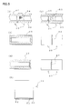
Fig. 5 is a cross section and a plane view showing the general configuration of the coupling portion for which another coupling member is used. - Next, the embodiments according to the present invention will be explained with reference to the drawings.
- As shown in
Fig. 1 (1), asolar cell module 10, according to the first embodiment of the present invention, is configured such that insulation tapes 53 are adhered to a firstsolar cell 20 and a secondsolar cell 20 so as to cover a connecting line betweenphotoelectrode substrates 30 and a connecting line betweencounter electrode substrates 40. - The
solar cell 20 will be explained with reference toFig. 2 andFig. 3 . - The
solar cell 20 includes aphotoelectrode substrate 30, acounter electrode substrate 40 facing thephotoelectrode substrate 30, acharge conveyance layer 50 provided in an area through which thesubstrates - The
photoelectrode substrate 30 is a substrate constituting a light incident surface. Thephotoelectrode substrate 30 includes a first base member 31, a first conductive film 32, a photoelectrode layer 33 configured to pass a charge generated from the sensitized dye due to the light irradiation, and a firstcurrent collecting line 34 configured to efficiently collect electrons. The first conductive film 32 and the photoelectrode layer 33 are sequentially formed on one surface of the first base member 31. The firstcurrent collecting line 34 is formed on a portion of the first conductive film 32 where the photoelectrode layer 33 is not formed, e.g., comb-shaped, in order to decrease loss due to the electric resistance. The first conductive film 32 and the firstcurrent collecting line 34 constitutes a first conductive layer. - The
counter electrode substrate 40 includes a second base member 41, a second conductive film 42, a catalyst layer 43 for improving the power generation efficiency, and a second current collectingline 44 configured to efficiently collect the generated electrons. The second conductive film 42 and the catalyst layer 43 are sequentially formed on one surface of the second base member 41. The second current collectingline 44 is formed, as is the firstcurrent collecting line 34, on a portion of the second conductive film 42 where the catalyst layer 43 is not formed, e.g., comb-shaped, in order to decrease the loss due to the electric resistance. The second conductive film 42 and the second current collectingline 44 constitute a second conductive layer. It should be noted that the firstcurrent collecting line 34 and the second current collectingline 44 are formed at positions facing each other in order to ensure an area as broad as possible, which will contribute to the generation. In addition, it is preferable that the firstcurrent collecting line 34 and the second current collectingline 44 should be covered by aninsulation layer 36. The reason is that theinsulation layer 36 prevents the corrosion due to the electrolyte, which is thecharge conveyance layer 50, and prevents a short circuit between thephotoelectrode substrate 30 and thecounter electrode substrate 40 through the firstcurrent collecting line 34 and the second current collectingline 44. - The
counter electrode substrate 40 is located with a certain gap from thephotoelectrode substrate 30 such that a surface on which the first conductive layer is formed and a surface on which the second conductive layer is formed face each other, and thecounter electrode substrate 40 is located so as to be displaced from thephotoelectrode substrate 30 such that the exposed portion of the firstconductive layer 35 and the exposed portion of the secondconductive layer 45 are defined. The exposed portion of the firstconductive layer 35 is made of the firstcurrent collecting line 34, and the exposed portion of the secondconductive layer 45 is made of the second current collectingline 44. - Next, members constituting the
solar cell 20 will be explained. - The first base member 31 preferably has high transparency because it is a light incident surface, and it can be made of glass having high transparency, tempered glass, synthesized resin having high transparency such as polycarbonate resin, acrylic resin, polyacrylate resin, polymethacrylate, and polyvinyl chloride. Furthermore, in addition to later-described polyethylene terephthalate resin having a high durability against the
charge conveyance layer 50, polyester synthetic resin such as polybutylene terephthalate resin and polyethylene naphthalate resin, and polyolefin synthetic resin such as polyethylene, polypropylene, and cyclic polyolefin resin may be properly used. - As a material of the first conductive film 32, there is no limitation only if it has excellent conductivity. It may be made of tin-doped indium oxide (ITO), fluorine-doped tin oxide (FTO), antimony-doped tin oxide (ATO), gold, platinum and so on, and a combination of them. The first conductive film 32 is formed with a vacuum evaporation method, a sputtering method, an ion plating, a CVD method, a migration electrodeposition method and so on.
- The photoelectrode layer 33 is formed of the minute particles of metallic oxide that holds the sensitizing dye. It is preferable that the minute particles of metallic oxide should be porous having through holes in order to hold the sensitizing dye.
- As a material of the first
current collecting line 34 and the second current collectingline 44, paste including metallic materials such as silver can be used, for example. As theinsulation layer 36 covering the firstcurrent collecting line 34 and the second current collectingline 44, glass frit or resin can be used. In this case, paste such as glass frit is pasted onto the firstcurrent collecting line 34 and the second current collectingline 44, and is burned so as to form theinsulation layer 36. - The second base member 41 can be formed using the same material as that of the first base member 31.
- The second conductive film 42 may be formed using the same material as that of the first conductive film 32, and with the same method of forming the first conductive film. In addition, when the catalyst layer 43 is formed on the second conductive film 42, as a material for the catalyst layer 43, a layer made of the deposited platinum, organic matters such as polyaniline, polythiophene, and polypyrrole may be used.
- The
charge conveyance layer 50 may be made of conducting materials that can convey ions. As a suitable material, for example, there are liquid electrolyte, solid electrolyte, and gel electrolyte. The liquid electrolyte have only to be liquid including redox species, and the ones which can be generally used for batteries or solar cells can be used, and is not particularly limited. The solid electrolyte may be conducting materials that can convey electrons, holes, and ions, and that may be used as an electrolyte of the solar cell without liquidity. The gel electrolyte is typically composed of electrolyte and gelling agent, and the above-described solid electrolyte can be used as an electrolyte. - Next, the method of manufacturing the
solar cell 20 will be explained. - First, a porous semiconductor layer made of minute particles of metallic oxide is formed on the first conductive film 32, which is formed on one surface of the first base member 31. The sensitizing dye is held by the porous semiconductor layer so as to make the photoelectrode layer 33. Furthermore, paste including metallic materials such as silver is pasted onto a portion of the first conductive film 32 where the photoelectrode layer 33 is not formed, and is burned so as to make the first
current collecting line 34. Paste such as glass frit is pasted onto the firstcurrent collecting line 34 and is burned so as to make theinsulation layer 36. As described above, thephotoelectrode substrate 30 is obtained. - Next, the catalyst layer 43 such as a platinum film is coated onto the second conductive film 42 formed on one surface of the second base member 41. Then, as is the first
current collecting line 34, paste including metallic materials such as silver is pasted onto a portion of the second conductive film 42 where the catalyst layer 43 is not formed, and is burned so as to form the second current collectingline 44. Paste such as glass frit is pasted on the second current collectingline 44, and is burned so as to form theinsulation layer 36. As described above, thecounter electrode substrate 40 is obtained. - Next, the
photoelectrode substrate 30 and thecounter electrode substrate 40 are located such that the surface on which the first conductive film 32 is formed and the surface on which the second conductive film 42 is formed faces each other. At this time, thephotoelectrode substrate 30 and thecounter electrode substrate 40 are located so as to be displaced from each other such that the exposed portion of the firstconductive layer 35 made of the firstcurrent collecting line 34 and the exposed portion of the secondconductive layer 45 made of the second current collectingline 44 are defined. - The
insulation layer 36 is not formed on the firstcurrent collecting line 34 and the second current collectingline 44, which constitute the exposed portion of the firstconductive layer 35 and the exposed portion of the secondconductive layer 45, in order to ensure the conduction with the later-described metallic plate or metallic tape 52. Indeed, as shown inFig. 3 , ends of the firstcurrent collecting line 34 and the second current collectingline 44, which constitute the exposed portion of the firstconductive layer 35 and exposed portion of the secondconductive layer 45, may be covered with theinsulation layer 36. The purpose of the above-described structure is to protect the firstcurrent collecting line 34 and the second current collectingline 44 from the corrosion due to the electrolyte when the later-described electrolyte is injected through both ends of the exposed portion of the firstconductive layer 35 and the exposed portion of the secondconductive layer 45. - It should be noted that first
current collecting line 34 and the second current collectingline 44 do not necessarily have to be formed if the electric resistance of the first conductive film 32 and the second conductive film 42 is within a permissible limit in terms of product characteristics. In a case where the firstcurrent collecting line 34 and the second current collectingline 44 are not formed, the exposed portion of the firstconductive layer 35 and the exposed portion of the secondconductive layer 45 are constituted by the first conductive film 32 and the second conductive film 42, respectively. - Finally, electrolytes are injected into the area through which
photoelectrode substrate 30 and thecounter electrode substrate 40 face each other in order to form thecharge conveyance layer 50. The side surfaces of the area through which thephotoelectrode substrate 30 and thecounter electrode substrate 40 face each other is sealed by the sealant 51 such as epoxy resin. It should be noted that if thecharge conveyance layer 50 is made of the liquid electrolyte, the sealant 51 is provided to seal the area through which thephotoelectrode substrate 30 and thecounter electrode substrate 40 face each other in order to prevent the battery leakage of the liquid electrolyte. In contrast, if the solid electrolyte or the gel electrolyte is employed, the sealant 51 does not necessarily have to be formed. As described above, thesolar cell 20 is obtained. - The
solar cell module 10, which is made by coupling at least twosolar cells 20 made with the above-described manufacturing method, will be explained with reference toFig. 1, Fig. 2 , andFig. 3 . - As shown in
Fig. 2 , thesolar cell module 10 includes the metallic plate or metallic tape 52, as the conductive member which does not have adhesiveness, located so as to keep in contact with the firstcurrent collecting line 35 as the exposed portion of the first conductive layer of the firstsolar cell 20 and the second current collectingline 45 as the exposed portion of the second conductive layer of the secondsolar cell 20. Thesolar cell module 10 further includes the insulation tape 53 as the coupling member that couples the firstsolar cell 20 and the secondsolar cell 20 such that the metallic plate or metallic tape 52 keeps in contact with them. - The metallic plate or metallic tape 52 is a conductive member that conducts the first
solar cell 20 and the secondsolar cell 20, and it is made of a thin plate-like or band-like metal which does not have adhesiveness. The metallic plate or metallic tape 52 is located such that its one surface keeps in contact with the firstcurrent collecting line 35 as the exposed portion of the first conductive layer of the firstsolar cell 20, and that its another surface keeps in contact with ins the second current collectingline 45 as the exposed portion of the second conductive layer of the secondsolar cell 20. Since the metallic plate or metallic tape is used, it becomes easy to evenly define the thickness, so that the variation of the electric resistance of thesolar cell module 10 will be lost. In addition, since the metallic plate or metallic tape is a material easy to obtain, it is possible to manufacture it at low cost. - The insulation tape 53, as the coupling member, couples the first
solar cell 20 with the secondsolar cell 20. The insulation tape 53 has an adhesive layer on its one surface, and the adhesive layer side is adhered to the surfaces of thesolar cells 20, so as to cover the connecting line between thephotoelectrode substrates 30 of the firstsolar cell 20 and the secondsolar cell 20, and the connecting line between thecounter electrode substrates 40 of the firstsolar cell 20 and the secondsolar cell 20. Since the insulation tape 53 is used, it is possible to couple the solar cell module by just adhering the firstsolar cell 20 to the secondsolar cell 20. Accordingly, it is not necessary to make a special processing to the substrate, thereby decreasing the number of the processes. - It should be noted that although the
photoelectrode substrates 30 of the firstsolar cell 20 and the secondsolar cell 20 are coupled with each other with a gap and thecounter electrode substrates 40 of the firstsolar cell 20 and the secondsolar cell 20 are coupled with each other with a gap as shown inFig. 2 , they can be coupled without gaps. - Next, members constituting the
solar cell module 10 will be explained. - Materials of the metallic plate or metallic tape 52, as the conductive member which does not have adhesiveness, may be various metals such as copper, aluminum, and iron. The thickness of the metallic plate or metallic tape 52 is preferably the same as a gap between the
photoelectrode substrate 30 and thecounter electrode substrate 40. If the thickness is larger than the gap, it is impossible to couple the firstsolar cell 20 with the secondsolar cell 20 so as to be flush with each other. The metallic plate or metallic tape 52 can be formed so as to have a thickness of 50 to 200 µm, for example, so as to correspond to the gap between thephotoelectrode substrate 30 and thecounter electrode substrate 40. - In addition, length and width of the metallic plate or metallic tape 52 only have to be within the exposed portion of the first
conductive layer 35 and the exposed portion of the secondconductive layer 45, i.e., they are not particularly limited. As shown inFig. 3 , in order to prevent the corrosion due to the injection of the electrolyte, in a case where theinsulation layer 36 covers both ends of the firstcurrent collecting line 34 as the exposed portion of the firstconductive layer 35 and the second current collectingline 44 as the exposed portion of the secondconductive layer 45, the metallic plate or metallic tape 52 is formed so as to have a length which rests within a portion where theinsulation layer 36 is not formed. - The material of the insulation tape 53 is only have to be an adhesive tape having insulation, and is not particularly limited. An adhesive tape can be employed that includes a base member made of polyimide film, epoxy film, polytetrafluoroethylene film, polyester film, glass cloth and so on, and an adhesive layer layered on the base member, made of acrylic adhesive, heat curing type silicone adhesive, heat curing type rubber adhesive, and so on. Since the insulation material is employed, it is possible to surely prevent a short circuit between the
photoelectrode substrates 30 of the firstsolar cell 20 and the secondsolar cell 20, and a short circuit between thecounter electrode substrates 40 of the firstsolar cell 20 and the secondsolar cell 20. - It is preferable to form the width of the insulation tape 53 such that the insulation tape 53 is not overlapped with the photoelectrode layer 33 when disposed, thereby not impeding the power generation.
- Next, with reference to
Fig. 1 (2), a method of manufacturing thesolar cell module 10 having the twosolar cells 20 coupled with each other will be explained. - First, two
solar cells 20 are prepared. Regarding the firstsolar cell 20, the metallic plate or metallic tape 52 is disposed such that its one surface gets into contact with the firstcurrent collecting line 34 as the exposed portion of the firstconductive layer 35. It should be noted that although the metallic plate or metallic tape 52 is disposed on the firstcurrent collecting line 34 as the exposed portion of the firstconductive layer 35 inFig. 1 (2), the metallic plate or metallic tape 52 may be disposed on the second current collectingline 44 as the exposed portion of the secondconductive layer 45. - Next, the first
current collecting line 34 as the exposed portion of the firstconductive layer 35 or the second current collectingline 44 as exposed portion of the secondconductive layer 45 of the firstsolar cell 20 on which the metallic plate or metallic tape 52 is placed, is overlapped with the second current collectingline 44 as the exposed portion of the secondconductive layer 45 or the firstcurrent collecting line 34 as the exposed portion of the firstconductive layer 35 of the secondsolar cell 20, via the metallic plate or metallic tape 52. Accordingly, another surface of the metallic plate or metallic tape 52 of the firstsolar cell 20 keeps in contact with the second current collectingline 44 as the exposed portion of the secondconductive layer 45 or the firstcurrent collecting line 34 as the exposed portion of the firstconductive layer 35, which ensures conduction between the firstsolar cell 20 and the secondsolar cell 20. - Finally, the insulation tape 53 is adhered so as to cover the connecting line between the
photoelectrode substrates 30 of the twosolar cells 20, and the connecting line between thecounter electrode substrates 40 of the twosolar cells 20, such that both surfaces of the metallic plate or metallic tape 52 keeps in contact with the firstcurrent collecting line 34 as the exposed portion of the firstconductive layer 35 or the second current collectingline 44 as the exposed portion of the secondconductive layer 45 of the firstsolar cell 20, and the second current collectingline 44 as the exposed portion of the secondconductive layer 45 or the firstcurrent collecting line 34 as the exposed portion of the firstconductive layer 35 of the secondsolar cell 20. As described above, thesolar cell module 10 is obtained. When three or moresolar cells 20 are to be coupled with each other, the above-described method can be employed. - Accordingly, regarding the
solar cell module 10 manufactured with the above-described method, the conductive adhesive is not used for coupling thesolar cell module 10. Accordingly, the electric resistance between the firstsolar cell 20 and the secondsolar cell 20 is decreased. Furthermore, since the processes of pasting and curing the conductive adhesive become unnecessary, the number of the processes is decreased and the manufacturing becomes easy. - In the
solar cell module 10 according to the second embodiment of the present invention, the second base member 41 and the second conductive film 42, which is the second conductive layer, is composed of one member having conductivity, and may be composed of various metallic plates such as titanium and aluminum. - As shown in
Fig. 4 , metallic plates used for the second base member 41 and the second conductive film 42, which is and the second conductive layer, are made of a material having low electric resistance. Therefore, it is not necessary to form the second current collectingline 44. Accordingly, the second base member 41 and the second conductive film 42, which is and the second conductive layer, constitute the exposed portion of the secondconductive layer 45. - In addition, in the
solar cell module 10 according to the second embodiment of the present invention, it is necessary to couple the firstsolar cell 20 with the secondsolar cell 20 with a gap therebetween. The purpose of the above-described structure is to prevent a short circuit between thecounter electrode substrates 40 of the firstsolar cell 20 and the secondsolar cell 20 due to the contact. - It should be noted that the same numerals are assigned to constituent elements the same as the constituent elements shown in
Fig. 2 . In addition, the explanation redundant with the constituent elements of thesolar cell 20 and the method of manufacturing thesolar cell module 10 shown inFig. 2 will be omitted. - It should be noted that although the metallic plate or metallic tape 52 is employed as the conductive member in the first embodiment and the second embodiment, the shape of the conductive member is not limited to a thin plate or band. A thread metallic wire can be employed, for example.
- Although the insulation tape 53 is employed as the coupling member in the first embodiment and the second embodiment, the coupling member is not limited to the insulation tape 53. A member that can couple the substrates of the
solar cells 20 is a coupling member according to the present invention. - For example, as shown in
Fig. 5 (1), screw holes may be formed on thephotoelectrode substrate 30 and thecounter electrode substrate 40, and a screw and nut 54 may be used for the coupling. In another example, as shown inFig. 5 (2), engaging portions 55, made of a convex portion and a concave portion, may be formed on thephotoelectrode substrate 30 of the firstsolar cell 20 and thecounter electrode substrate 40 of the secondsolar cell 20, and they may be engaged with each other. In this case, the convex portion and the concave portion may be either formed on thephotoelectrode substrate 30 of the firstsolar cell 20 or thecounter electrode substrate 40 of the secondsolar cell 20. In addition, as shown inFig. 5 (3), the substrates of the firstsolar cell 20 and the secondsolar cell 20 may be coupled by an annular band 56. As shown inFig. 5 (4), instead of the band 56, a U-shaped clip 57 may be used. In addition, as shown inFig. 5 (5), aglass ribbon 58 having a thickness of several tens µm may be located around the metallic plate or metallic tape 52 disposed on the exposed portion of the firstconductive layer 35 of the firstsolar cell 20. Theglass ribbon 58 is heated and deposited to couple the firstsolar cell 20 with the secondsolar cell 20. In this case, theglass ribbon 58 can be replaced with adhesive. It should be noted that although the metallic plate or metallic tape 52 is disposed on the exposedportion 34 of the first conductive layer of the firstsolar cell 10 and theglass ribbon 58 is disposed around the metallic plate or metallic tape 52 inFig. 5 (5), if the metallic plate 52 is disposed on the exposed portion of the secondconductive layer 45, theglass ribbon 58 will be also disposed on the exposed portion of the secondconductive layer 45. -
- 10
- solar cell module
- 20
- solar cell
- 30
- photoelectrode substrate
- 31
- first base member
- 32
- first conductive film
- 33
- photoelectrode layer
- 34
- first current collecting line
- 35
- exposed portion of first conductive layer
- 36
- insulation layer
- 40
- counter electrode substrate
- 41
- second base member
- 42
- second conductive film
- 43
- catalyst layer
- 44
- second current collecting line
- 45
- exposed portion of second conductive layer
- 50
- charge conveyance layer
- 51
- sealant
- 52
- metallic plate or metallic tape
- 53
- insulation tape
- 54
- screw and nut
- 55
- engaging portion
- 56
- band
- 57
- clip
- 58
- glass ribbon
Claims (7)
- A solar cell module comprising at least two dye-sensitized solar cells coupled with each other,
each of the solar cells comprises:a photoelectrode substrate including a first base member, and a first conductive layer and a photoelectrode layer sequentially formed on one surface of the photoelectrode substrate;a counter electrode substrate including a second base member and a second conductive layer formed on one surface of the second base member, the counter electrode substrate being located with a certain space from the photoelectrode substrate so as to face the surface on which the first conductive layer is formed, and the counter electrode substrate being located to be displaced from the photoelectrode substrate such that an exposed portion of the first conductive layer and an exposed portion of the second conductive layer are defined; anda charge conveyance layer provided in the certain space,the solar cell module further comprising:a conductive member which does not have adhesiveness, the conductive member being located so as to keep in contact with the exposed portion of the first conductive layer of a first solar cell and the exposed portion of the second conductive layer of a second solar cell; anda coupling member coupling the first solar cell with the second solar cell such that the conductive member keeps in contact with the exposed portions. - The solar cell module according to claim 1, wherein the first conductive layer includes a first conductive film, and a first current collecting line formed on a portion of the first conducive film where the photoelectrode layer is not formed, and
the exposed portion of the first conductive layer is made of the first current collecting line. - The solar cell module according to claim 1 or 2, wherein the second conductive layer includes a second conductive film, and a second current collecting line formed on the second conductive layer, and
the exposed portion of the second conductive layer is made of the second current collecting line. - The solar cell module according to claim 1 or 2, wherein the second base member and the second conductive layer formed on the one surface of the second base member are metallic plates.
- The solar cell module according to any of claims 1 through 4, wherein the conductive member is a metallic plate or a metallic tape.
- The solar cell module according to any of claims 1 through 4, wherein the coupling member is an insulation tape adhered so as to cover a connecting line between the substrates of the first solar cell and the second solar cell.
- A method of manufacturing a solar cell module having at least two dye-sensitized solar cells connected with each other, wherein
each of the solar cells comprises:a photoelectrode substrate including a first base member, and a first conductive layer and a photoelectrode layer sequentially formed on one surface of the first base member;a counter electrode substrate including a second base member, and a second conductive layer formed on one surface of the second base member, the counter electrode substrate being located with a certain space from the photoelectrode substrate so as to face the surface on which the first conductive layer is formed, and being displaced from the photoelectrode substrate such that an exposed portion of the first conductive layer and an exposed portion of the second conductive layer are defined; anda charge conveyance layer provided in the certain space,the method comprising steps of:disposing a conductive member on the exposed portion of the first conductive layer or the exposed portion of the second conductive layer of a first solar cell;locating a second solar cell such that the exposed portion of the second conductive layer or the exposed portion of the first conductive layer of the second solar cell is overlapped with the disposed conductive member; andcoupling the first solar cell with the second solar cell by a coupling member such that the conductive member keeps in contact with the exposed portions of the first solar cell and the second solar cell.
Applications Claiming Priority (2)
| Application Number | Priority Date | Filing Date | Title |
|---|---|---|---|
| JP2012101673A JP5656910B2 (en) | 2012-04-26 | 2012-04-26 | Solar cell module and connection method thereof |
| PCT/JP2013/053841 WO2013161355A1 (en) | 2012-04-26 | 2013-02-18 | Solar cell module and method for connecting same |
Publications (2)
| Publication Number | Publication Date |
|---|---|
| EP2843755A1 true EP2843755A1 (en) | 2015-03-04 |
| EP2843755A4 EP2843755A4 (en) | 2016-01-27 |
Family
ID=49482697
Family Applications (1)
| Application Number | Title | Priority Date | Filing Date |
|---|---|---|---|
| EP13781625.2A Withdrawn EP2843755A4 (en) | 2012-04-26 | 2013-02-18 | SOLAR CELL MODULE AND CONNECTION METHOD THEREOF |
Country Status (8)
| Country | Link |
|---|---|
| US (1) | US20150114469A1 (en) |
| EP (1) | EP2843755A4 (en) |
| JP (1) | JP5656910B2 (en) |
| KR (1) | KR20150015432A (en) |
| CN (1) | CN104246937B (en) |
| AU (1) | AU2013254025A1 (en) |
| TW (1) | TWI535046B (en) |
| WO (1) | WO2013161355A1 (en) |
Family Cites Families (19)
| Publication number | Priority date | Publication date | Assignee | Title |
|---|---|---|---|---|
| JP2004119305A (en) * | 2002-09-27 | 2004-04-15 | Hitachi Maxell Ltd | Photoelectric conversion element and photoelectric conversion element module using the same |
| EP1560272B1 (en) * | 2004-01-29 | 2016-04-27 | Panasonic Intellectual Property Management Co., Ltd. | Solar cell module |
| US7781672B2 (en) * | 2004-06-01 | 2010-08-24 | Konarka Technologies, Inc. | Photovoltaic module architecture |
| JP4636890B2 (en) * | 2005-01-24 | 2011-02-23 | 積水樹脂株式会社 | Dye-sensitized solar cell |
| KR100658730B1 (en) * | 2005-11-30 | 2006-12-15 | 삼성에스디아이 주식회사 | Solar cell |
| JP2007265635A (en) * | 2006-03-27 | 2007-10-11 | Sekisui Jushi Co Ltd | Solar cell connection method and dye-sensitized solar cell |
| JP2007265634A (en) * | 2006-03-27 | 2007-10-11 | Sekisui Jushi Co Ltd | Dye-sensitized solar cell |
| JP2008251517A (en) * | 2007-03-02 | 2008-10-16 | Tokyo Univ Of Science | Dye-sensitized solar cell module and method for producing photoelectrode used therefor |
| WO2009044786A1 (en) * | 2007-10-02 | 2009-04-09 | Shimane Prefectural Government | Integration type dye-sensitized solar cell module and method for manufacturing the same |
| KR20100075552A (en) * | 2007-11-02 | 2010-07-02 | 니폰 가야꾸 가부시끼가이샤 | Dye-sensitized solar cell module |
| JP2009245705A (en) * | 2008-03-31 | 2009-10-22 | Koito Mfg Co Ltd | Dye-sensitized solar cell |
| JP2009272168A (en) * | 2008-05-08 | 2009-11-19 | Nok Corp | Dye-sensitized solar cell |
| JP5320853B2 (en) * | 2008-06-25 | 2013-10-23 | Tdk株式会社 | Photoelectric conversion element |
| JP2010113905A (en) * | 2008-11-05 | 2010-05-20 | Sony Corp | Dye-sensitized solar cell and process for producing the same |
| CN102341952A (en) * | 2009-03-06 | 2012-02-01 | 日本电气株式会社 | Photoelectric conversion element and manufacturing method thereof, optical sensor and solar cell |
| KR20110043454A (en) * | 2009-10-20 | 2011-04-27 | 주식회사 동진쎄미켐 | Manufacturing method of dye-sensitized solar cell module using foil and dye-sensitized solar cell manufactured thereby |
| JP4811527B1 (en) * | 2010-07-07 | 2011-11-09 | 大日本印刷株式会社 | Dye-sensitized solar cell module |
| JP2013012366A (en) * | 2011-06-29 | 2013-01-17 | Sony Corp | Photoelectric conversion element module, method for manufacturing photoelectric conversion element module and electronic apparatus |
| JP2013114778A (en) * | 2011-11-25 | 2013-06-10 | Sony Corp | Photoelectric conversion element, photoelectric conversion element module, photoelectric conversion element module manufacturing method, electronic equipment, and building |
-
2012
- 2012-04-26 JP JP2012101673A patent/JP5656910B2/en not_active Expired - Fee Related
-
2013
- 2013-02-18 KR KR20147026462A patent/KR20150015432A/en not_active Ceased
- 2013-02-18 AU AU2013254025A patent/AU2013254025A1/en not_active Abandoned
- 2013-02-18 EP EP13781625.2A patent/EP2843755A4/en not_active Withdrawn
- 2013-02-18 US US14/396,705 patent/US20150114469A1/en not_active Abandoned
- 2013-02-18 CN CN201380020547.1A patent/CN104246937B/en not_active Expired - Fee Related
- 2013-02-18 WO PCT/JP2013/053841 patent/WO2013161355A1/en not_active Ceased
- 2013-04-23 TW TW102114310A patent/TWI535046B/en not_active IP Right Cessation
Also Published As
| Publication number | Publication date |
|---|---|
| TW201405849A (en) | 2014-02-01 |
| JP5656910B2 (en) | 2015-01-21 |
| WO2013161355A1 (en) | 2013-10-31 |
| JP2013229246A (en) | 2013-11-07 |
| KR20150015432A (en) | 2015-02-10 |
| CN104246937B (en) | 2017-03-22 |
| US20150114469A1 (en) | 2015-04-30 |
| CN104246937A (en) | 2014-12-24 |
| AU2013254025A1 (en) | 2014-10-23 |
| EP2843755A4 (en) | 2016-01-27 |
| TWI535046B (en) | 2016-05-21 |
Similar Documents
| Publication | Publication Date | Title |
|---|---|---|
| CN101682100B (en) | Dye-sensitized solar battery module and method for manufacturing the same | |
| CN102106032B (en) | Photoelectric conversion element module and method for manufacturing photoelectric conversion element module | |
| CN101842934B (en) | Dye-sensitized solar cell module | |
| CN109564823B (en) | Solar cell module | |
| EP2346054A2 (en) | Photoelectric Conversion Module | |
| KR100384893B1 (en) | Nano-particle oxide solar cells and fabrication method of the same and solar cell modules and transparent electric window using the same | |
| CN201302932Y (en) | Electrode structure of dye-sensitized solar cell | |
| CN104380408B (en) | Dye-sensitized solar cell element | |
| US8742248B2 (en) | Photoelectric conversion module and method of manufacturing the same | |
| JP2014130807A (en) | Dye-sensitized solar cell module | |
| JP2007265635A (en) | Solar cell connection method and dye-sensitized solar cell | |
| US8916770B2 (en) | Photoelectric conversion device | |
| JP5128118B2 (en) | Wet solar cell and manufacturing method thereof | |
| EP2367188A2 (en) | Photoelectric conversion module | |
| EP2407984A2 (en) | Photoelectric conversion module | |
| US20150114469A1 (en) | Solar cell module and method for connecting same | |
| CN104781895A (en) | Dye-sensitized solar cell element | |
| JP2001267595A (en) | Solar cell module | |
| JP2010218935A (en) | Solar cell module | |
| US20130104955A1 (en) | Photoelectric conversion module | |
| KR101034217B1 (en) | Dye-sensitized solar cell manufacturing method and dye-sensitized solar cell manufactured thereby | |
| CN108231421B (en) | Dye-sensitized photovoltaic cell, module and manufacturing method thereof | |
| KR20100104552A (en) | Dye sensitized solar cell module and method of preparing the same | |
| JP5160854B2 (en) | Method for producing dye-sensitized solar cell element | |
| JP2020038876A (en) | Electric module |
Legal Events
| Date | Code | Title | Description |
|---|---|---|---|
| PUAI | Public reference made under article 153(3) epc to a published international application that has entered the european phase |
Free format text: ORIGINAL CODE: 0009012 |
|
| 17P | Request for examination filed |
Effective date: 20141120 |
|
| AK | Designated contracting states |
Kind code of ref document: A1 Designated state(s): AL AT BE BG CH CY CZ DE DK EE ES FI FR GB GR HR HU IE IS IT LI LT LU LV MC MK MT NL NO PL PT RO RS SE SI SK SM TR |
|
| AX | Request for extension of the european patent |
Extension state: BA ME |
|
| DAX | Request for extension of the european patent (deleted) | ||
| RA4 | Supplementary search report drawn up and despatched (corrected) |
Effective date: 20160107 |
|
| RIC1 | Information provided on ipc code assigned before grant |
Ipc: H01M 14/00 20060101AFI20151222BHEP Ipc: H01M 2/20 20060101ALI20151222BHEP Ipc: H01L 31/04 20060101ALI20151222BHEP |
|
| STAA | Information on the status of an ep patent application or granted ep patent |
Free format text: STATUS: THE APPLICATION IS DEEMED TO BE WITHDRAWN |
|
| 18D | Application deemed to be withdrawn |
Effective date: 20160806 |