EP2843089A1 - SiC SINGLE CRYSTAL SUBSTRATE - Google Patents
SiC SINGLE CRYSTAL SUBSTRATE Download PDFInfo
- Publication number
- EP2843089A1 EP2843089A1 EP13780614.7A EP13780614A EP2843089A1 EP 2843089 A1 EP2843089 A1 EP 2843089A1 EP 13780614 A EP13780614 A EP 13780614A EP 2843089 A1 EP2843089 A1 EP 2843089A1
- Authority
- EP
- European Patent Office
- Prior art keywords
- single crystal
- polished surface
- sic substrate
- polishing
- substrate
- Prior art date
- Legal status (The legal status is an assumption and is not a legal conclusion. Google has not performed a legal analysis and makes no representation as to the accuracy of the status listed.)
- Granted
Links
Images




Classifications
-
- H—ELECTRICITY
- H10—SEMICONDUCTOR DEVICES; ELECTRIC SOLID-STATE DEVICES NOT OTHERWISE PROVIDED FOR
- H10D—INORGANIC ELECTRIC SEMICONDUCTOR DEVICES
- H10D62/00—Semiconductor bodies, or regions thereof, of devices having potential barriers
- H10D62/50—Physical imperfections
- H10D62/57—Physical imperfections the imperfections being on the surface of the semiconductor body, e.g. the body having a roughened surface
-
- C—CHEMISTRY; METALLURGY
- C30—CRYSTAL GROWTH
- C30B—SINGLE-CRYSTAL GROWTH; UNIDIRECTIONAL SOLIDIFICATION OF EUTECTIC MATERIAL OR UNIDIRECTIONAL DEMIXING OF EUTECTOID MATERIAL; REFINING BY ZONE-MELTING OF MATERIAL; PRODUCTION OF A HOMOGENEOUS POLYCRYSTALLINE MATERIAL WITH DEFINED STRUCTURE; SINGLE CRYSTALS OR HOMOGENEOUS POLYCRYSTALLINE MATERIAL WITH DEFINED STRUCTURE; AFTER-TREATMENT OF SINGLE CRYSTALS OR A HOMOGENEOUS POLYCRYSTALLINE MATERIAL WITH DEFINED STRUCTURE; APPARATUS THEREFOR
- C30B29/00—Single crystals or homogeneous polycrystalline material with defined structure characterised by the material or by their shape
- C30B29/10—Inorganic compounds or compositions
- C30B29/36—Carbides
-
- C—CHEMISTRY; METALLURGY
- C09—DYES; PAINTS; POLISHES; NATURAL RESINS; ADHESIVES; COMPOSITIONS NOT OTHERWISE PROVIDED FOR; APPLICATIONS OF MATERIALS NOT OTHERWISE PROVIDED FOR
- C09K—MATERIALS FOR MISCELLANEOUS APPLICATIONS, NOT PROVIDED FOR ELSEWHERE
- C09K3/00—Materials not provided for elsewhere
- C09K3/14—Anti-slip materials; Abrasives
- C09K3/1454—Abrasive powders, suspensions and pastes for polishing
- C09K3/1463—Aqueous liquid suspensions
-
- C—CHEMISTRY; METALLURGY
- C30—CRYSTAL GROWTH
- C30B—SINGLE-CRYSTAL GROWTH; UNIDIRECTIONAL SOLIDIFICATION OF EUTECTIC MATERIAL OR UNIDIRECTIONAL DEMIXING OF EUTECTOID MATERIAL; REFINING BY ZONE-MELTING OF MATERIAL; PRODUCTION OF A HOMOGENEOUS POLYCRYSTALLINE MATERIAL WITH DEFINED STRUCTURE; SINGLE CRYSTALS OR HOMOGENEOUS POLYCRYSTALLINE MATERIAL WITH DEFINED STRUCTURE; AFTER-TREATMENT OF SINGLE CRYSTALS OR A HOMOGENEOUS POLYCRYSTALLINE MATERIAL WITH DEFINED STRUCTURE; APPARATUS THEREFOR
- C30B33/00—After-treatment of single crystals or homogeneous polycrystalline material with defined structure
-
- H—ELECTRICITY
- H10—SEMICONDUCTOR DEVICES; ELECTRIC SOLID-STATE DEVICES NOT OTHERWISE PROVIDED FOR
- H10D—INORGANIC ELECTRIC SEMICONDUCTOR DEVICES
- H10D62/00—Semiconductor bodies, or regions thereof, of devices having potential barriers
- H10D62/80—Semiconductor bodies, or regions thereof, of devices having potential barriers characterised by the materials
- H10D62/83—Semiconductor bodies, or regions thereof, of devices having potential barriers characterised by the materials being Group IV materials, e.g. B-doped Si or undoped Ge
- H10D62/832—Semiconductor bodies, or regions thereof, of devices having potential barriers characterised by the materials being Group IV materials, e.g. B-doped Si or undoped Ge being Group IV materials comprising two or more elements, e.g. SiGe
- H10D62/8325—Silicon carbide
-
- H—ELECTRICITY
- H10—SEMICONDUCTOR DEVICES; ELECTRIC SOLID-STATE DEVICES NOT OTHERWISE PROVIDED FOR
- H10P—GENERIC PROCESSES OR APPARATUS FOR THE MANUFACTURE OR TREATMENT OF DEVICES COVERED BY CLASS H10
- H10P52/00—Grinding, lapping or polishing of wafers, substrates or parts of devices
- H10P52/40—Chemomechanical polishing [CMP]
- H10P52/403—Chemomechanical polishing [CMP] of conductive or resistive materials
-
- H—ELECTRICITY
- H10—SEMICONDUCTOR DEVICES; ELECTRIC SOLID-STATE DEVICES NOT OTHERWISE PROVIDED FOR
- H10P—GENERIC PROCESSES OR APPARATUS FOR THE MANUFACTURE OR TREATMENT OF DEVICES COVERED BY CLASS H10
- H10P90/00—Preparation of wafers not covered by a single main group of this subclass, e.g. wafer reinforcement
- H10P90/12—Preparing bulk and homogeneous wafers
- H10P90/129—Preparing bulk and homogeneous wafers by polishing
Definitions
- This invention relates to a single crystal SiC (silicon carbide) substrate, particularly a single crystal SiC substrate capable of forming a good epitaxial thin film thereon to provide a high-quality epitaxial substrate.
- SiC silicon carbide
- GaN or diamond gallium carbide
- SiC has been attracting attention as a semiconductor material operable in a severe environment, such as a high temperature environment, that precluded the use of conventional Si semiconductors.
- Production of a single crystal SiC substrate includes slicing an SiC single crystal ingot into wafers, grinding the as-cut wafer to a predetermined thickness using, e.g., a grinder, lapping the wafer with abrasive grains, e.g., of diamond, and polishing the lapped wafer with finer abrasive grains to provide a mirror finish.
- abrasive grains e.g., of diamond
- the production involves the step of removing a work damaged layer resulting from the grinding or lapping steps from the surface of the substrate.
- CMP chemical mechanical polishing
- Patent Literature 4 proposes a process for producing an SiC epitaxial substrate including polishing a single crystal SiC substrate until the disturbed lattice layer is reduced to 3 nm or thinner, cleaning the polished substrate at a high temperature in a hydrogen atmosphere, and epitaxially growing a thin film of silicon carbide on the cleaned substrate.
- Patent Literature 4 in which the disturbed lattice layer on the surface of a single crystal SiC substrate is removed as much as possible by polishing before the formation of an epitaxial thin film of silicon carbide, is thought to provide a high quality-epitaxial thin film. Reduction of the disturbed lattice layer on the surface of a single crystal SiC substrate assuredly seems to result in removal of the damaged layer. And yet, it is still considered that there is a room for further investigation into factors other than the disturbed lattice layer on a polished single crystal SiC substrate in order to form a more defect-free, high-quality epitaxial thin film.
- Non-Patent Literatures 1 and 2 report that a CMP treatment of an SiC substrate with an alkaline slurry containing MnO 2 and MnO 4 - accelerates oxidation reaction, resulting in an improved processing rate.
- the reports are silent on the possibility of obtaining an SiC substrate with a highly precisely polished surface to a conventionally unreachable level by performing a CMP treatment under a specific condition.
- the present inventors have intensively studied on a damaged layer of a polished surface of a single crystal SiC substrate. As a result, they have succeeded in finding a lattice defect that has not been observed by conventional methods by observing a cross-section of a single crystal SiC substrate under reflections from a specific direction using a transmission electron microscope. They have also found that the thus observed lattice defect is largely influential on the quality of an epitaxial thin film and the production yield of electronic devices.
- the lattice defect the inventors Unlike the known defects of a single crystal SiC substrate, such as scratches or roughness of a polished surface and the disturbed lattice layer dealt with in Patent Literature 4, the lattice defect the inventors have found intrudes fairly deeply from the polished surface and is believed to originate from a damaged layer. The inventors have ascertained that the lattice defect originating from a damaged layer can be eliminated almost completely by a specific CMP treatment to remove the damaged layer at a high speed without imposing a great burden to the crystal per se of a single crystal SiC substrate.
- the present invention relates a single crystal SiC substrate having a CMP-treated polished surface, the single crystal SiC substrate having 5 or fewer lattice defects, which have a width of 30 nm or more in a direction parallel to the polished surface and a length of 50 nm or more in a direction perpendicular to the polished surface when observed in cross-section using a transmission electron microscope under the 00L reflection or the h-h0 reflection, where L and h are each an integer other than 0.
- the number of the lattice defects is counted within an area of 10 ⁇ m in a direction parallel to the polished surface and from the polished surface to a depth of 100 nm in a direction perpendicular to the polished surface.
- the single crystal SiC substrate according to the invention has almost no lattice defects on its surface side and therefore allows for formation of a satisfactory epitaxial thin film thereon.
- the single crystal SiC substrate of the invention is identified through cross-sectional observation using transmission electron microscope (hereinafter sometimes abbreviated as TEM).
- TEM is a microscopy technique in which a beam of electrons is transmitted through a specimen, the transmitted electrons are converged by an electron lens to form an image, and the image is magnified at a magnification of about several thousands of times to one-million times.
- the thickness of the specimen In order to allow an electron beam to pass through a specimen, the thickness of the specimen must be 200 nm or less in the direction normal to the plane of observation.
- the single crystal SiC substrate is sliced using, e.g., a focused ion beam (FIB) system.
- FIB focused ion beam
- the lattice defect according to the invention can be confirmed by conducting TEM observation of a cross-section of the CMP treated single crystal substrate under the 00L reflection or the h-h0 reflection, wherein L and h are each an integer except 0.
- the bar in Miller indices indicates a minus sign for the trailing index.
- the value L is preferably a multiple of 4. It is more preferred that the TEM observation be conducted under the 004 or 1-10 reflection.
- the above discussed TEM observation allows for finding a lattice defect that occurs from the surface (polished surface) of the CMP treated single crystal SiC substrate in the direction of thickness of the substrate.
- the inventors' study has revealed that a single crystal SiC substrate having been CMP treated in a conventional manner, namely, using colloidal silica abrasive grains shows a number of the lattice defects extending from the polished surface in the thickness direction when observed on its cross-section.
- the substrate is incapable of forming a good epitaxial thin film thereon even if generation of such lattice defects is controlled.
- the inventors have ascertained that, in order to form a good epitaxial thin film, it is necessary for the substrate to have almost no such lattice defects generating from the polished surface in the thickness direction, specifically to have 5 or fewer above-identified lattice defects (the lattice defects observable by TEM under the above described specific condition) within a length of 10 ⁇ m in a direction parallel to the polished surface and a depth of 100 nm in a direction perpendicular to the polished surface.
- the number of the lattice defects is preferably 3 or fewer, more preferably 1 or fewer, most preferably zero.
- lattic defect denotes a site having a slight deviation from an ideal three-dimensional array of atoms or a site having a distortion of crystal lattice of an SiC single crystal, specifically a defect due to lack of an atom, distortion, or disturbance of atomic layers induced by machining, such as grinding and lapping, in the vicinity of the polished surface. It is heretofore known by cross-sectional observation that a single crystal SiC substrate has defects from its surface toward inside. However, generally known defects that have been studied are small defects generated in the vicinity of the polished surface in the final stage of polishing. For example, Patent Literature 4 deals with defects of 3 nm or smaller.
- the lattice defect as referred to in the invention is a site recognizable as a vacancy, distortion or disturbance existing in the crystal structure of a TEM image of a cross-sectional of a single crystal SiC substrate and having a width of 30 nm or more in a direction parallel to the polished surface and a length (or depth) of 50 nm or more in the direction perpendicular to the polished surface.
- This type of a lattice defect is considered ascribable to a great load applied to the single crystal SiC substrate during grinding or lapping. Because the above-identified lattice defect intrudes deep into the inside of the substrate, it would be necessary to relatively deeply polish the surface without imposing a large load to the crystal per se in order to remove it.
- the single crystal SiC substrate of the invention is obtained by CMP treatment using a polishing slurry comprising manganese oxide particles and a solution containing manganate ions.
- Slurry containing both solid manganese oxide particles and dissolved manganate ions exhibits high polishing performance in polishing a high hardness workpiece, such as silicon carbide or gallium nitride, and is thereby capable of efficiently removing lattice defects derived from a damaged layer.
- suitable manganate ions include MnO 4 - , MnO 4 2- , MnO 4 3- , and MnO 4 6- , with permanganate ion (MnO 4 - ) being particularly preferred for its high oxidation performance.
- a polishing slurry containing manganese dioxide particles (MnO 2 ) and permanganate ions (MnO 4 - ) exhibits especially high polishing performance.
- the manganate ion concentration of the solution in the polishing slurry is preferably 0.5 mass% or more, more preferably 1.0 mass% or more.
- the polishing slurry having the recited manganate ion concentration exhibits particularly high polishing performance. While a higher manganate ion concentration leads to higher polishing performance, the concentration is preferably 40 mass% or less more preferably 20 mass% or less, even more preferably 10 mass% or less, in order to secure safety on handling the polishing slurry.
- the manganate ion content in the polishing slurry is measured by ion chromatography or absorptiometry.
- the content of the manganese oxide particles is preferably 1.0 mass% or more, more preferably 2.0 mass% or more.
- the polishing slurry having the recited manganese oxide particles content exhibits particularly high polishing performance.
- the content is preferably 35 mass% or less, more preferably 10 mass% or less, in order to secure suitable fluidity in handling the polishing slurry.
- the ratio of manganate ion to manganese oxide in the polishing slurry is preferably 1/5 or higher, more preferably 1/2 or higher, by molar concentration. At a ratio falling within that range, a good equilibrium balance is obtained between the atoms in the manganese oxide particles and the manganate ions, and generation of the lattice defects observable through TEM observation under the specific condition is prevented effectively.
- the upper limit of the molar concentration ratio of manganate ions to manganese oxide is, while not influential on the polishing performance of the polishing material, preferably 5 or less, more preferably 4 or less, in order to avoid more use of expensive manganate ions than necessary in the interests of economy.
- the molar concentration of manganese oxide is obtained by converting the mass of the individual manganese oxide particles to an amount of substance using the corresponding molecular weight and dividing the amount of substance by the mass of a solvent.
- the molar concentration of the substance supplying manganate ions can be calculated in the same manner as for manganese oxide.
- the polishing slurry preferably contains an alkali metal ion such as sodium or potassium ion.
- alkali metal ion such as sodium or potassium ion.
- the existence of alkali metal ions allows the manganate ions to exist stably in the slurry while maintaining higher oxidation state.
- the molar ratio of the alkali metal ion, if present, to the manganate ion in the polishing slurry is preferably 1:1 to 6:1.
- the solution of the polishing slurry is preferably neutral to alkaline, i.e., has a pH of 7 or more for the following reason.
- manganate ions contained in the polishing slurry of the invention are known to exhibit high oxidizing performance in an acidic solution, manganese particles coexisting with manganate ions have difficulty in maintaining a dispersed state in an acidic condition and tend to agglomerate to scratch the workpiece.
- the single crystal SiC substrate of the invention has a surface with minimal lattice defects and is therefore capable of forming a more defect-free, high quality epitaxial thin film thereon to provide a high quality epitaxial substrate.
- a polishing slurry was prepared by mixing 20 g of electrolytic MnO 2 (D 50 : 0.30 ⁇ m; specific surface area: 48.7 m 2 /g; crystallite size: 2.0 nm; crystal structure: ⁇ -MnO 2 ; available from Mitsui Mining & Smelting Co., Ltd.) and 980 g of pure water and adding 9.8 g of KMnO 4 (from Wako Pure Chemical Industries, Ltd.), followed by stirring.
- the same electrolytic MnO 2 was used in Examples 2 through 10 and Comparative Examples 1 to 3.
- the crystallite size was measured by the Scherrer method.
- the specific surface area was measured by the BET method.
- the average particle size D 50 is a diameter at 50% cumulative volume in the particle size distribution measured by a laser diffraction scattering method.
- the oxide particles were dispersed by ultrasonication for 3 minutes before the measurement.
- a laser diffraction scattering particle size analyzer, LA-920 from Horiba, Ltd. was used.
- a CMP test was carried out using the thus prepared polishing slurry under the following conditions.
- a 2-inch lapped 4H-SiC substrate was used as a workpiece to be polished. The Si-face of the substrate was polished.
- a single side polisher BC-15 from MAT Inc. was used as a polishing device.
- a polishing pad SUBA #600 available from Nitta Haas Inc. was attached onto the platen. The platen was rotated at 60 rpm with a peripheral speed of 7163 cm/min. The carrier was rotated at 60 rpm with a peripheral speed of 961 cm/min.
- the load applied during polishing was 200 gf/cm 2 .
- the polishing slurry was fed at a rate of 200 ml/min.
- the polishing time was 3 hours.
- the surface roughness Ra (JIS B0601) before and after polishing was obtained by measuring the surface profile of the substrate using an atomic force microscope Dimension 3100 from Digital Instruments and analyzing the measurement data using software NanoScope 5V from the same maker.
- the scanning range and points were 10 ⁇ m ⁇ 10 ⁇ m and 512 ⁇ 512, respectively.
- the scanning rate was 1 Hz.
- the polishing rate (nm/min) was calculated from the difference in mass between before and after the polishing and the density of SiC (3.10 g/cm 3 ). The results are shown in Table 1.
- a cross-section of the polished substrate was observed as follows. An about 8 mm-side square was cut out of the polished substrate such that at least one of the cross-sections was the (110) plane. A 100 nm thick specimen was sliced along the (110) plane using an FIB system, FB200 from Hitachi High-Technologies. The specimen was observed using a transmission electron microscope JEM-ARM200F from JEOL, Ltd. The magnifications in the ⁇ 110> direction observation ( Fig. 1A ) and in bright-field observation under the 004 reflection ( Fig. 1B ) were 200,000, and the magnification in dark-field observation under the 1-10 reflection ( Fig. 1C ) was 50,000. The same cross-sectional observation was conducted in Examples 2 through 13 and Comparative Examples 1 to 3.
- Example 1 The procedure of Example 1 was followed, except for changing the amount of KMnO 4 to 29.4 g.
- the results of evaluation are shown in Table 1.
- Example 1 The procedure of Example 1 was followed, except for changing the amount of KMnO 4 to 58.8 g.
- the results of evaluation are shown in Table 1.
- a polishing slurry was prepared by mixing 40 g of electrolytic MnO 2 powder and 960 g of pure water, adding thereto 28.8 g of KMnO 4 , followed by stirring.
- the CMP test was conducted in the same manner as in Example 1, except for using the resulting polishing slurry. The results of evaluation are shown in Table 1.
- Example 4 The procedure of Example 4 was repeated, except for changing the amount of KMnO 4 to 57.6 g.
- the results of evaluation are shown in Table 1.
- a polishing slurry was prepared by mixing 100 g of electrolytic MnO 2 powder and 900 g of pure water, adding thereto 54.0 g of KMnO 4 , followed by stirring.
- the CMP test was conducted in the same manner as in Example 1, except for using the resulting polishing slurry. The results of evaluation are shown in Table 1.
- Example 1 The procedure of Example 1 was repeated, except for changing the amount of KMnO 4 to 7.35 g. The results of evaluation are shown in Table 1.
- Example 1 The procedure of Example 1 was repeated, except for changing the amount of KMnO 4 to 9.8 g. The results of evaluation are shown in Table 1.
- Example 1 The procedure of Example 1 was repeated, except for changing the amount of KMnO 4 to 14.7 g. The results of evaluation are shown in Table 1.
- Example 1 The procedure of Example 1 was repeated, except for changing the amount of KMnO 4 to 19.6 g. The results of evaluation are shown in Table 1.
- Lambda-MnO 2 powder (D 50 : 0.72 ⁇ m; specific surface area: 16.0 m 2 /g; crystallite size: 70 nm) obtained by acid-cleaning lithium manganate (LiMn 2 O 4 ) (from Mitsui Mining & Smelting) in a 0.1 N HNO 3 solution at 95°C for 120 minutes was used as polishing grains.
- a polishing slurry was prepared by mixing 20 g of the ⁇ -MnO 2 and 980 g of pure water, adding thereto 29.4 g of KMnO 4 (from Wako Pure Chemical), followed by stirring.
- the CMP test was conducted in the same manner as in Example 1, except for using the resulting polishing slurry. The results of evaluation are shown in Table 1.
- Mn 2 O 3 powder (D 50 :1.77 ⁇ m; specific surface area: 4.0 m 2 /g; crystallite size: 9.7 nm) obtained by firing the electrolytic MnO 2 powder used in Example 1 at 800°C was used as polishing grains.
- a polishing slurry was prepared by mixing 20 g of the Mn 2 O 3 powder and 980 g of pure water, adding thereto 29.4 g of KMnO 4 , followed by stirring.
- the CMP test was conducted in the same manner as in Example 1, except for using the resulting polishing slurry. The results of evaluation are shown in Table 1.
- a polishing slurry was prepared by mixing 20 g of Mn 3 O 4 powder (D 50 : 1.04 ⁇ m; specific surface area: 4.9 m 2 /g; crystallite size: 9.6 nm; available from Mitsui Mining & Smelting) and 980 g of pure water, adding thereto 29.4 g of KMnO 4 , followed by stirring.
- the CMP test was conducted in the same manner as in Example 1, except for using the resulting polishing slurry. The results of evaluation are shown in Table 1.
- Example 2 A CMP test and cross-sectional observation were performed in the same manner as in Example 1, except for using a colloidal silica slurry DSC1001 from Fujimi Inc. as a polishing slurry.
- the polishing characteristics are shown in Table 1.
- Cross-sectional TEM images are shown in Figs. 2A, 2B, and 2C .
- a commercially available 2-inch 4H-SiC substrate was lapped on its Si face.
- Lapping was carried out in the same manner as in the CMP test of Example 1, except for using, as a polishing slurry, a diamond slurry 1/2PCS-WB2 from Nano Factor Co., Ltd.
- the lapping time was 10 minutes.
- the resulting lapped substrate was observed on its cross-section in the same manner as in Example 1.
- the TEM images are shown in Figs. 3A through 3C .
- the substrate used in Example 1 and Comparative Example 1 as a workpiece to be CMP-treated was the same as this lapped substrate.
- a commercially available 2-inch 4H-SiC substrate having an epiready finish (a surface ready to receive thereon epitaxial growth of thin film) was observed on its cross-section in the same manner as in Example 1.
- the TEM images are shown in Figs. 4A through 4C .
- Comparative Example 4 corresponds to the technique of Non-Patent Literature 1.
- a polishing slurry was prepared by mixing 50 g of electrolytic MnO 2 powder and 950 g of pure water, adding thereto 14.5 g of KMnO 4 , followed by stirring.
- the polishing performance was evaluated in the same manner as in Example 1, except for using the thus prepared polishing slurry and changing the rotational speed of the platen to 90 rpm. The results obtained are shown in Table 1.
- Example 1 MnO 2 1.98 0.23 0.73 0.06 0.270 8.1 9.28 0.133
- Example 2 1.94 0.23 2.15 0.19 0.809 8.0 12.35 0.122
- Example 3 1.89 0.23 4.18 0.38 1.617 9.0 12.17 0.104
- Example 4 3.89 0.48 2.11 0.19 0.396 8.6 11.90 0.136
- Example 5 3.78 0.48 4.10 0.38 0.792 8.6 12.50 0.132
- Example 6 9.49 1.28 3.86 0.38 0.297 9.1 10.73 0.122
- Example 7 1.99 0.23 0.55 0.05 0.202 7.8 9.57 0.068
- Example 8 1.98 0.23 0.73 0.06 0.270 7.6 9.37 0.077
- Example9 1.97 0.23 1.09 0.09 0.404 7.6 10.73 0.079
- Example 10 1.96 0.23 1.45 0.13 0.539 7.9 11.19 0.075
- Example 11 ⁇ -MnO 2 1.94 0.23 2.15 0.19 0.810 7.9 8.30 0.126
- Example 1 SiO 2 26.7 - 0 0 - 7.2 0.22 0.570 Compara.
- Example 4 MnO 2 5.00 0.61 0.10 0.1 0.170 11.0 2.08 -
- A Manganate ion concentration in slurry (mol/l)
- B Manganese ion concentration in polishing grains of slurry (mol/l)
- FIG. 1A An interpretation on the TEM images of Figs. 1A through 1C is given below.
- the central diagonal line from upper left to lower right in Fig. 1A is the boundary of the specimen.
- the right upper part above the diagonal line is the SiC single crystal structure.
- the right upper part above the central diagonal line in Figs. 1B and 1C is the single crystal SiC substrate side. The same applies to Figs. 2A through 4C .
- the ⁇ 110> direction TEM image taken in Comparative Example 1 shows a site with a slight disturbance in polished surface smoothness.
- the bright-field TEM image taken under the 004 reflection shown in Fig. 2B provides confirmation of the presence of a site (lattice defect) having a distortion 30 nm or more in width (in the direction parallel to the diagonal line in the TEM image) and 50 nm or more in length (in the direction perpendicular to the diagonal line).
- Comparative Example 2 dealt with a lapping treatment before a CMP treatment with intent to observe the condition of a work damaged layer after the lapping.
- TEM observation was made in the ⁇ 110> direction
- presence of a large concave defect on the polished surface was revealed as shown in Fig. 3A .
- the bright-field TEM image under the 004 reflection ( Fig. 3B ) provides confirmation of the presence of a site (lattice defect) with a distortion 40 nm or more in width in the direction parallel to the diagonal line and 20 nm or more in length in the direction perpendicular to the diagonal line.
- the dark-field TEM image under the 1-10 reflection Fig.
- the central diagonal line from upper left to lower right in Figs. 5 and 6 is the boundary of the specimen. In these drawings, too, the right upper part above the diagonal line is the SiC single crystal structure.
- the sites indicated by the arrows were regarded as lattice defects, and the number of them was counted.
- a count was taken within an area of 100 nm in a direction perpendicular to the polished surface by 10 ⁇ m from the polished surface in a direction parallel to the polished surface (the direction of the diagonal line of the TEM image).
- the specimen of Comparative Example 1 at 5 locations, there were at least 6 and, in some locations, about 20 to 30 lattice defects in a 10 ⁇ m long area.
- the observed lattice defects were within a depth of 100 nm from the polished surface.
- the CMP-treated substrate of Example 1 was inspected for the number of lattice defects in the same manner. Seeing that the substrate of Example 1 had no lattice defect as demonstrated in Figs. 1A to 1C , the number of lattice defects within a length of 10 ⁇ m along the direction parallel to the polished surface (the direction of the diagonal line in TEM images) was zero.
- Figs. 7A through 7D TEM images of the substrate of Comparative Example 4, which represents the technique of Non-Patent Literature 1 are shown in Figs. 7A through 7D .
- Fig. 7A shows a cross-section taken in the ⁇ 110> direction, in which the dark left upper half is the substrate side.
- Figs. 7B , 7C, and 7D are bright-field TEM images ( ⁇ 200,000) under the 004 reflection of the sites numbered 1 to 3, respectively, in Fig. 7A .
- Figs. 7B to 7D provide confirmation of the presence of a site (lattice defect) with a distortion 30 nm or wider in the direction of the diagonal line in the TEM images and 50 nm or longer in the direction perpendicular to the diagonal line.
- the present invention allows for efficient production of a high quality epitaxial substrate.
Landscapes
- Chemical & Material Sciences (AREA)
- Engineering & Computer Science (AREA)
- Materials Engineering (AREA)
- Organic Chemistry (AREA)
- Crystallography & Structural Chemistry (AREA)
- Metallurgy (AREA)
- Inorganic Chemistry (AREA)
- Mechanical Treatment Of Semiconductor (AREA)
- Finish Polishing, Edge Sharpening, And Grinding By Specific Grinding Devices (AREA)
- Crystals, And After-Treatments Of Crystals (AREA)
Abstract
Description
- This invention relates to a single crystal SiC (silicon carbide) substrate, particularly a single crystal SiC substrate capable of forming a good epitaxial thin film thereon to provide a high-quality epitaxial substrate.
- SiC (silicon carbide) is a kind of wide band gap semiconductors similar to GaN or diamond. Having high heat and chemical resistance and excellent mechanical strength, SiC has been attracting attention as a semiconductor material operable in a severe environment, such as a high temperature environment, that precluded the use of conventional Si semiconductors. In recent years, there has been an increasing demand for a single crystal SiC substrate for use in high-frequency, high-voltage resistant electronic devices.
- Production of a single crystal SiC substrate includes slicing an SiC single crystal ingot into wafers, grinding the as-cut wafer to a predetermined thickness using, e.g., a grinder, lapping the wafer with abrasive grains, e.g., of diamond, and polishing the lapped wafer with finer abrasive grains to provide a mirror finish.
- The production involves the step of removing a work damaged layer resulting from the grinding or lapping steps from the surface of the substrate. In order to remove the damaged layer, it has been a practice generally followed to perform chemical mechanical polishing (CMP) using colloidal silica as abrasive grains.
- If there is a defect, such as a damaged layer, on the surface of a single crystal SiC substrate on which an epitaxial thin film is to be formed, it would be difficult to well accomplish epitaxial growth, making it hard to provide an epitaxial substrate with desired characteristics and reliability. Therefore, it has been a practice to remove the damaged layer by chemical mechanical polishing (CMP) using colloidal silica abrasive grains as described in
Patent Literature 1. A damaged layer is said to be present from the substrate surface to a depth of several hundreds of nanometers. Under the present circumstances, a long time is needed to achieve the CMP treatment because of the low polishing rate of colloidal silica abrasive grains. - In order to securely remove the damaged layer, it has been proposed to perform vapor phase etching in combination with a CMP treatment as disclosed in
Patent Literatures - Cases are sometimes met with in which even a single crystal SiC substrate having been CMP treated for a long period of time fails to form a satisfactory epitaxial thin film. This has caused a reduction in yield of production of electronic devices involving formation of an epitaxial thin film. To perform vapor phase etching as in
Patent Literatures - The technique of Patent Literature 4, in which the disturbed lattice layer on the surface of a single crystal SiC substrate is removed as much as possible by polishing before the formation of an epitaxial thin film of silicon carbide, is thought to provide a high quality-epitaxial thin film. Reduction of the disturbed lattice layer on the surface of a single crystal SiC substrate assuredly seems to result in removal of the damaged layer. And yet, it is still considered that there is a room for further investigation into factors other than the disturbed lattice layer on a polished single crystal SiC substrate in order to form a more defect-free, high-quality epitaxial thin film.
-
Non-Patent Literatures -
- Patent Literature 1:
JP 2007-311586A - Patent Literature 2:
JP 2008-227534A - Patent Literature 3:
JP 2006-261563A - Patent Literature 4:
JP 2011-49496A - Non-Patent Literature:
-
- Non-Patent Literature 1: Article entitled "Single Crystal SiC CMP Using Manganese Slurry" by Hasegawa Tadashi, et al., Transactions of the JSPE (The Japan Society for Precision Engineering) 2011, vol. 2011, E33
- Non-Patent Literature 2: Article entitled "Application of Manganese slurry to CMP Process of SiC Substrate" by Hasegawa Tadashi, et al., Proceedings of the JSME (The Japan Society of Mechanical Engineers) Kyushu Branch 2010, vol. 63, pp. 95-96
- In the light of the above circumstances, it is an object of the invention to provide a single crystal SiC substrate capable of securely forming a good epitaxial thin film thereon to provide a high quality epitaxial substrate.
- In order to accomplish the above object, the present inventors have intensively studied on a damaged layer of a polished surface of a single crystal SiC substrate. As a result, they have succeeded in finding a lattice defect that has not been observed by conventional methods by observing a cross-section of a single crystal SiC substrate under reflections from a specific direction using a transmission electron microscope. They have also found that the thus observed lattice defect is largely influential on the quality of an epitaxial thin film and the production yield of electronic devices. Unlike the known defects of a single crystal SiC substrate, such as scratches or roughness of a polished surface and the disturbed lattice layer dealt with in Patent Literature 4, the lattice defect the inventors have found intrudes fairly deeply from the polished surface and is believed to originate from a damaged layer. The inventors have ascertained that the lattice defect originating from a damaged layer can be eliminated almost completely by a specific CMP treatment to remove the damaged layer at a high speed without imposing a great burden to the crystal per se of a single crystal SiC substrate.
- The present invention relates a single crystal SiC substrate having a CMP-treated polished surface, the single crystal SiC substrate having 5 or fewer lattice defects, which have a width of 30 nm or more in a direction parallel to the polished surface and a length of 50 nm or more in a direction perpendicular to the polished surface when observed in cross-section using a transmission electron microscope under the 00L reflection or the h-h0 reflection, where L and h are each an integer other than 0. The number of the lattice defects is counted within an area of 10 µm in a direction parallel to the polished surface and from the polished surface to a depth of 100 nm in a direction perpendicular to the polished surface.
- The single crystal SiC substrate according to the invention has almost no lattice defects on its surface side and therefore allows for formation of a satisfactory epitaxial thin film thereon.
- The single crystal SiC substrate of the invention is identified through cross-sectional observation using transmission electron microscope (hereinafter sometimes abbreviated as TEM). TEM is a microscopy technique in which a beam of electrons is transmitted through a specimen, the transmitted electrons are converged by an electron lens to form an image, and the image is magnified at a magnification of about several thousands of times to one-million times. In order to allow an electron beam to pass through a specimen, the thickness of the specimen must be 200 nm or less in the direction normal to the plane of observation. The single crystal SiC substrate is sliced using, e.g., a focused ion beam (FIB) system. The lattice defect according to the invention can be confirmed by conducting TEM observation of a cross-section of the CMP treated single crystal substrate under the 00L reflection or the h-h0 reflection, wherein L and h are each an integer except 0. In the description of the invention, the bar in Miller indices indicates a minus sign for the trailing index. The value L is preferably a multiple of 4. It is more preferred that the TEM observation be conducted under the 004 or 1-10 reflection.
- The above discussed TEM observation allows for finding a lattice defect that occurs from the surface (polished surface) of the CMP treated single crystal SiC substrate in the direction of thickness of the substrate. The inventors' study has revealed that a single crystal SiC substrate having been CMP treated in a conventional manner, namely, using colloidal silica abrasive grains shows a number of the lattice defects extending from the polished surface in the thickness direction when observed on its cross-section. As a result of further study, it has been found that the substrate is incapable of forming a good epitaxial thin film thereon even if generation of such lattice defects is controlled. The inventors have ascertained that, in order to form a good epitaxial thin film, it is necessary for the substrate to have almost no such lattice defects generating from the polished surface in the thickness direction, specifically to have 5 or fewer above-identified lattice defects (the lattice defects observable by TEM under the above described specific condition) within a length of 10 µm in a direction parallel to the polished surface and a depth of 100 nm in a direction perpendicular to the polished surface. The number of the lattice defects is preferably 3 or fewer, more preferably 1 or fewer, most preferably zero.
- The term "lattice defect" as used herein denotes a site having a slight deviation from an ideal three-dimensional array of atoms or a site having a distortion of crystal lattice of an SiC single crystal, specifically a defect due to lack of an atom, distortion, or disturbance of atomic layers induced by machining, such as grinding and lapping, in the vicinity of the polished surface. It is heretofore known by cross-sectional observation that a single crystal SiC substrate has defects from its surface toward inside. However, generally known defects that have been studied are small defects generated in the vicinity of the polished surface in the final stage of polishing. For example, Patent Literature 4 deals with defects of 3 nm or smaller. In contrast, the lattice defect as referred to in the invention is a site recognizable as a vacancy, distortion or disturbance existing in the crystal structure of a TEM image of a cross-sectional of a single crystal SiC substrate and having a width of 30 nm or more in a direction parallel to the polished surface and a length (or depth) of 50 nm or more in the direction perpendicular to the polished surface. This type of a lattice defect is considered ascribable to a great load applied to the single crystal SiC substrate during grinding or lapping. Because the above-identified lattice defect intrudes deep into the inside of the substrate, it would be necessary to relatively deeply polish the surface without imposing a large load to the crystal per se in order to remove it. Although a defect near the surface could be removed by hydrogen etching, hydrogen etching if performed on the lattice defect of interest of the invention is liable to produce an additional lattice defect under the influence of the heat applied in hydrogen etching, resulting in an increase of lattice defects. It is believed therefore that, even if hydrogen etching is conducted to remove the lattice defect intruding deep inside the substrate, elimination of such a lattice defect would not be accomplished.
- The single crystal SiC substrate of the invention is obtained by CMP treatment using a polishing slurry comprising manganese oxide particles and a solution containing manganate ions. Slurry containing both solid manganese oxide particles and dissolved manganate ions exhibits high polishing performance in polishing a high hardness workpiece, such as silicon carbide or gallium nitride, and is thereby capable of efficiently removing lattice defects derived from a damaged layer.
- Examples of the manganese oxide particles that can be used in the production of the single crystal SiC substrate of the invention include particles of manganese (II) oxide (MnO), dimanganese (III) trioxide (Mn2O3), manganese dioxide (MnO2), and trimanganese tetroxide (Mn3O4), with particles of manganese dioxide being particularly preferred for their high oxidation power. Examples of suitable manganate ions include MnO4 -, MnO4 2-, MnO4 3-, and MnO4 6-, with permanganate ion (MnO4 -) being particularly preferred for its high oxidation performance. A polishing slurry containing manganese dioxide particles (MnO2) and permanganate ions (MnO4 -) exhibits especially high polishing performance.
- The manganate ion concentration of the solution in the polishing slurry is preferably 0.5 mass% or more, more preferably 1.0 mass% or more. The polishing slurry having the recited manganate ion concentration exhibits particularly high polishing performance. While a higher manganate ion concentration leads to higher polishing performance, the concentration is preferably 40 mass% or less more preferably 20 mass% or less, even more preferably 10 mass% or less, in order to secure safety on handling the polishing slurry. The manganate ion content in the polishing slurry is measured by ion chromatography or absorptiometry.
- The content of the manganese oxide particles is preferably 1.0 mass% or more, more preferably 2.0 mass% or more. The polishing slurry having the recited manganese oxide particles content exhibits particularly high polishing performance. The content is preferably 35 mass% or less, more preferably 10 mass% or less, in order to secure suitable fluidity in handling the polishing slurry.
- The ratio of manganate ion to manganese oxide in the polishing slurry is preferably 1/5 or higher, more preferably 1/2 or higher, by molar concentration. At a ratio falling within that range, a good equilibrium balance is obtained between the atoms in the manganese oxide particles and the manganate ions, and generation of the lattice defects observable through TEM observation under the specific condition is prevented effectively. The upper limit of the molar concentration ratio of manganate ions to manganese oxide is, while not influential on the polishing performance of the polishing material, preferably 5 or less, more preferably 4 or less, in order to avoid more use of expensive manganate ions than necessary in the interests of economy. The molar concentration of manganese oxide is obtained by converting the mass of the individual manganese oxide particles to an amount of substance using the corresponding molecular weight and dividing the amount of substance by the mass of a solvent. The molar concentration of the substance supplying manganate ions can be calculated in the same manner as for manganese oxide.
- The polishing slurry preferably contains an alkali metal ion such as sodium or potassium ion. The existence of alkali metal ions allows the manganate ions to exist stably in the slurry while maintaining higher oxidation state. The molar ratio of the alkali metal ion, if present, to the manganate ion in the polishing slurry is preferably 1:1 to 6:1.
- The solution of the polishing slurry is preferably neutral to alkaline, i.e., has a pH of 7 or more for the following reason. Although manganate ions contained in the polishing slurry of the invention are known to exhibit high oxidizing performance in an acidic solution, manganese particles coexisting with manganate ions have difficulty in maintaining a dispersed state in an acidic condition and tend to agglomerate to scratch the workpiece.
- The single crystal SiC substrate of the invention has a surface with minimal lattice defects and is therefore capable of forming a more defect-free, high quality epitaxial thin film thereon to provide a high quality epitaxial substrate.
-
- [
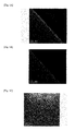
Fig. 1A] Fig. 1A is a <110> direction TEM image taken in Example 1. - [
Fig. 1B] Fig. 1B is a bright-field TEM image taken under the 004 reflection in Example 1. - [
Fig. 1C] Fig. 1C is a dark-field TEM image taken under the 1-10 reflection in Example 1. - [
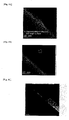
Fig.2A] Fig. 2A is a <110> direction TEM image taken in Comparative Example 1. - [
Fig. 2B] Fig. 2B is a bright-field TEM image taken under the 004 reflection in Comparative Example 1. - [
Fig. 2C] Fig. 2C is a dark-field TEM image taken under the 1-10 reflection in Comparative Example 1. - [
Fig. 3A] Fig. 3A is a <110> direction TEM image taken in Comparative Example 2. - [
Fig. 3B] Fig. 3B is a bright-field TEM image taken under the 004 reflection in Comparative Example 2. - [
Fig. 3C] Fig. 3C is a dark-field TEM image taken under the 1-10 reflection in Comparative Example 2. - [
Fig.4A] Fig. 4A is a <110> direction TEM image taken in Comparative Example 3. - [
Fig. 4B] Fig. 4B is a bright-field TEM image taken under the 004 reflection in Comparative Example 3. - [
Fig. 4C] Fig. 4C is a dark-field TEM image taken under the 1-10 reflection in Comparative Example 3. - [
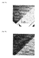
Fig. 5] Fig. 5 is a TEM image on which lattice defects were counted in Comparative Example 1. - [
Fig. 6] Fig. 6 is a TEM image on which lattice defects were counted in Comparative Example 1. - [
Fig. 7A] Fig. 7A is a <110> direction TEM image taken in Comparative Example 4. - [
Fig. 7B] Fig. 7B is a bright-field TEM image taken under the 004 reflection in Comparative Example 4. - [
Fig. 7C] Fig. 7C is a bright-field TEM image taken under the 004 reflection in Comparative Example 4. - [
Fig. 7D] Fig. 7D is a bright-field TEM image taken under the 004 reflection in Comparative Example 4. - The invention will be described by way of Examples.
- A polishing slurry was prepared by mixing 20 g of electrolytic MnO2 (D50: 0.30 µm; specific surface area: 48.7 m2/g; crystallite size: 2.0 nm; crystal structure: γ-MnO2; available from Mitsui Mining & Smelting Co., Ltd.) and 980 g of pure water and adding 9.8 g of KMnO4 (from Wako Pure Chemical Industries, Ltd.), followed by stirring. The same electrolytic MnO2 was used in Examples 2 through 10 and Comparative Examples 1 to 3. The crystallite size was measured by the Scherrer method. The specific surface area was measured by the BET method. The average particle size D50 is a diameter at 50% cumulative volume in the particle size distribution measured by a laser diffraction scattering method. In the measurement of particle size distribution, the oxide particles were dispersed by ultrasonication for 3 minutes before the measurement. A laser diffraction scattering particle size analyzer, LA-920 from Horiba, Ltd. was used.
- A CMP test was carried out using the thus prepared polishing slurry under the following conditions. A 2-inch lapped 4H-SiC substrate was used as a workpiece to be polished. The Si-face of the substrate was polished. A single side polisher BC-15 from MAT Inc. was used as a polishing device. A polishing pad SUBA #600 available from Nitta Haas Inc. was attached onto the platen. The platen was rotated at 60 rpm with a peripheral speed of 7163 cm/min. The carrier was rotated at 60 rpm with a peripheral speed of 961 cm/min. The load applied during polishing was 200 gf/cm2. The polishing slurry was fed at a rate of 200 ml/min. The polishing time was 3 hours.
- Evaluation after polishing was performed as follows. The surface roughness Ra (JIS B0601) before and after polishing was obtained by measuring the surface profile of the substrate using an atomic force microscope Dimension 3100 from Digital Instruments and analyzing the measurement data using software NanoScope 5V from the same maker. The scanning range and points were 10 µm × 10 µm and 512 × 512, respectively. The scanning rate was 1 Hz. The polishing rate (nm/min) was calculated from the difference in mass between before and after the polishing and the density of SiC (3.10 g/cm3). The results are shown in Table 1.
- A cross-section of the polished substrate was observed as follows. An about 8 mm-side square was cut out of the polished substrate such that at least one of the cross-sections was the (110) plane. A 100 nm thick specimen was sliced along the (110) plane using an FIB system, FB200 from Hitachi High-Technologies. The specimen was observed using a transmission electron microscope JEM-ARM200F from JEOL, Ltd. The magnifications in the <110> direction observation (
Fig. 1A ) and in bright-field observation under the 004 reflection (Fig. 1B ) were 200,000, and the magnification in dark-field observation under the 1-10 reflection (Fig. 1C ) was 50,000. The same cross-sectional observation was conducted in Examples 2 through 13 and Comparative Examples 1 to 3. - The procedure of Example 1 was followed, except for changing the amount of KMnO4 to 29.4 g. The results of evaluation are shown in Table 1.
- The procedure of Example 1 was followed, except for changing the amount of KMnO4 to 58.8 g. The results of evaluation are shown in Table 1.
- A polishing slurry was prepared by mixing 40 g of electrolytic MnO2 powder and 960 g of pure water, adding thereto 28.8 g of KMnO4, followed by stirring. The CMP test was conducted in the same manner as in Example 1, except for using the resulting polishing slurry. The results of evaluation are shown in Table 1.
- The procedure of Example 4 was repeated, except for changing the amount of KMnO4 to 57.6 g. The results of evaluation are shown in Table 1.
- A polishing slurry was prepared by mixing 100 g of electrolytic MnO2 powder and 900 g of pure water, adding thereto 54.0 g of KMnO4, followed by stirring. The CMP test was conducted in the same manner as in Example 1, except for using the resulting polishing slurry. The results of evaluation are shown in Table 1.
- The procedure of Example 1 was repeated, except for changing the amount of KMnO4 to 7.35 g. The results of evaluation are shown in Table 1.
- The procedure of Example 1 was repeated, except for changing the amount of KMnO4 to 9.8 g. The results of evaluation are shown in Table 1.
- The procedure of Example 1 was repeated, except for changing the amount of KMnO4 to 14.7 g. The results of evaluation are shown in Table 1.
- The procedure of Example 1 was repeated, except for changing the amount of KMnO4 to 19.6 g. The results of evaluation are shown in Table 1.
- Lambda-MnO2 powder (D50: 0.72 µm; specific surface area: 16.0 m2/g; crystallite size: 70 nm) obtained by acid-cleaning lithium manganate (LiMn2O4) (from Mitsui Mining & Smelting) in a 0.1 N HNO3 solution at 95°C for 120 minutes was used as polishing grains. A polishing slurry was prepared by mixing 20 g of the λ-MnO2 and 980 g of pure water, adding thereto 29.4 g of KMnO4 (from Wako Pure Chemical), followed by stirring. The CMP test was conducted in the same manner as in Example 1, except for using the resulting polishing slurry. The results of evaluation are shown in Table 1.
- Mn2O3 powder (D50:1.77 µm; specific surface area: 4.0 m2/g; crystallite size: 9.7 nm) obtained by firing the electrolytic MnO2 powder used in Example 1 at 800°C was used as polishing grains. A polishing slurry was prepared by mixing 20 g of the Mn2O3 powder and 980 g of pure water, adding thereto 29.4 g of KMnO4, followed by stirring. The CMP test was conducted in the same manner as in Example 1, except for using the resulting polishing slurry. The results of evaluation are shown in Table 1.
- A polishing slurry was prepared by mixing 20 g of Mn3O4 powder (D50: 1.04 µm; specific surface area: 4.9 m2/g; crystallite size: 9.6 nm; available from Mitsui Mining & Smelting) and 980 g of pure water, adding thereto 29.4 g of KMnO4, followed by stirring. The CMP test was conducted in the same manner as in Example 1, except for using the resulting polishing slurry. The results of evaluation are shown in Table 1.
- A CMP test and cross-sectional observation were performed in the same manner as in Example 1, except for using a colloidal silica slurry DSC1001 from Fujimi Inc. as a polishing slurry. The polishing characteristics are shown in Table 1. Cross-sectional TEM images are shown in
Figs. 2A, 2B, and 2C . - A commercially available 2-inch 4H-SiC substrate was lapped on its Si face. Lapping was carried out in the same manner as in the CMP test of Example 1, except for using, as a polishing slurry, a
diamond slurry 1/2PCS-WB2 from Nano Factor Co., Ltd. The lapping time was 10 minutes. The resulting lapped substrate was observed on its cross-section in the same manner as in Example 1. The TEM images are shown inFigs. 3A through 3C . The substrate used in Example 1 and Comparative Example 1 as a workpiece to be CMP-treated was the same as this lapped substrate. - A commercially available 2-inch 4H-SiC substrate having an epiready finish (a surface ready to receive thereon epitaxial growth of thin film) was observed on its cross-section in the same manner as in Example 1. The TEM images are shown in
Figs. 4A through 4C . - Comparative Example 4 corresponds to the technique of
Non-Patent Literature 1. A polishing slurry was prepared by mixing 50 g of electrolytic MnO2 powder and 950 g of pure water, adding thereto 14.5 g of KMnO4, followed by stirring. The polishing performance was evaluated in the same manner as in Example 1, except for using the thus prepared polishing slurry and changing the rotational speed of the platen to 90 rpm. The results obtained are shown in Table 1.Table 1 Polishing Slurry Results of Evaluation Polishing Grains Kind Polishing Grains Concn. (mass%) B (mol/L) Manganate Ion Concn. (mass%) A (mol/l) A/B pH Polishing Rate (nm/min) Surface Roughness Ra after Polishing (nm) Example 1 MnO2 1.98 0.23 0.73 0.06 0.270 8.1 9.28 0.133 Example 2 1.94 0.23 2.15 0.19 0.809 8.0 12.35 0.122 Example 3 1.89 0.23 4.18 0.38 1.617 9.0 12.17 0.104 Example 4 3.89 0.48 2.11 0.19 0.396 8.6 11.90 0.136 Example 5 3.78 0.48 4.10 0.38 0.792 8.6 12.50 0.132 Example 6 9.49 1.28 3.86 0.38 0.297 9.1 10.73 0.122 Example 7 1.99 0.23 0.55 0.05 0.202 7.8 9.57 0.068 Example 8 1.98 0.23 0.73 0.06 0.270 7.6 9.37 0.077 Example9 1.97 0.23 1.09 0.09 0.404 7.6 10.73 0.079 Example 10 1.96 0.23 1.45 0.13 0.539 7.9 11.19 0.075 Example 11 λ-MnO2 1.94 0.23 2.15 0.19 0.810 7.9 8.30 0.126 Example 12 Mn2O3 1.94 0.13 2.15 0.19 0.730 5.7 8.08 0.194 Example 13 Mn3O4 1.94 0.09 2.15 0.19 0.710 9.6 8.15 0.196 Compara. Example 1 SiO2 26.7 - 0 0 - 7.2 0.22 0.570 Compara. Example 4 MnO2 5.00 0.61 0.10 0.1 0.170 11.0 2.08 - A: Manganate ion concentration in slurry (mol/l)
B: Manganese ion concentration in polishing grains of slurry (mol/l) - An interpretation on the TEM images of
Figs. 1A through 1C is given below. The central diagonal line from upper left to lower right inFig. 1A is the boundary of the specimen. The right upper part above the diagonal line is the SiC single crystal structure. Likewise, the right upper part above the central diagonal line inFigs. 1B and 1C is the single crystal SiC substrate side. The same applies toFigs. 2A through 4C . - As displayed in
Fig. 1A , observation in the <110> direction gives confirmation of the SiC single crystal structure in which lattices are periodically stacked (a single layer has a thickness of about 1 nm) and the smooth polished surface of the single crystal SiC substrate. Neither the bright-field image under the 004 reflection shown inFig. 1B nor the dark-field image under the 1-10 reflection shown inFig. 1C reveals a site like a lattice defect. - While not shown in the drawings, it was confirmed that the single crystal SiC substrate obtained in Examples 2 through 13 had a smooth polished surface similarly to that of Example 1. Furthermore, no site like a lattice defect was observed at all in each of the bright-field and dark-field image under the 004 and 1-10 reflections, respectively.
- In contrast to this, the <110> direction TEM image taken in Comparative Example 1, in which the CMP treatment was carried out using colloidal silica, shows a site with a slight disturbance in polished surface smoothness. The bright-field TEM image taken under the 004 reflection shown in
Fig. 2B provides confirmation of the presence of a site (lattice defect) having adistortion 30 nm or more in width (in the direction parallel to the diagonal line in the TEM image) and 50 nm or more in length (in the direction perpendicular to the diagonal line). The presence of a site (lattice defect) with adistortion 30 nm or more in width (in the direction parallel to the diagonal line in the TEM image) and 50 nm or more in length (in the direction perpendicular to the diagonal line) is also confirmed on the dark-field TEM image under the 1-10 reflection shown inFig. 2C . - Comparative Example 2 dealt with a lapping treatment before a CMP treatment with intent to observe the condition of a work damaged layer after the lapping. When TEM observation was made in the <110> direction, presence of a large concave defect on the polished surface was revealed as shown in
Fig. 3A . The bright-field TEM image under the 004 reflection (Fig. 3B ) provides confirmation of the presence of a site (lattice defect) with a distortion 40 nm or more in width in the direction parallel to the diagonal line and 20 nm or more in length in the direction perpendicular to the diagonal line. Similarly, the dark-field TEM image under the 1-10 reflection (Fig. 3C ) also provides confirmation of the presence of a site (lattice defect) with a distortion 40 nm or wider in the direction parallel to the diagonal line and 50 nm or deeper in the direction perpendicular to the diagonal line. It was thus confirmed that the single crystal SiC substrate before being subjected to the CMP treatment of Example 1 obviously has a defect derived from work damage. - In Comparative Example 3, a commercially available epiready substrate was observed. As shown in
Fig. 4A , a site like a lattice defect was not obviously found on the polished surface when observed in the <110> direction as shown inFig. 4A . However, in bright-field observation under the 004 reflection (Fig. 4B ), the presence of a site (lattice defect) with adistortion 30 nm or more in width in the direction parallel to the diagonal line and 20 nm or more in length in the direction perpendicular to the diagonal line was confirmed. The presence of a site (lattice defect) with a distortion of 40 nm or more in width in the direction parallel to the diagonal line and about 20 nm in depth in the direction perpendicular to the diagonal line was confirmed in dark-field observation under the 1-10 reflection. -
Figs. 5 and 6 are bright-field TEM images taken of the single crystal SiC substrate of Comparative Example 1 under the g = [004] reflection at a magnification of 20,000 times, on which the number of lattice defects was counted. The central diagonal line from upper left to lower right inFigs. 5 and 6 is the boundary of the specimen. In these drawings, too, the right upper part above the diagonal line is the SiC single crystal structure. InFigs. 5 and 6 , the sites indicated by the arrows were regarded as lattice defects, and the number of them was counted. A count was taken within an area of 100 nm in a direction perpendicular to the polished surface by 10 µm from the polished surface in a direction parallel to the polished surface (the direction of the diagonal line of the TEM image). As a result of examining the specimen of Comparative Example 1 at 5 locations, there were at least 6 and, in some locations, about 20 to 30 lattice defects in a 10 µm long area. The observed lattice defects were within a depth of 100 nm from the polished surface. The CMP-treated substrate of Example 1 was inspected for the number of lattice defects in the same manner. Seeing that the substrate of Example 1 had no lattice defect as demonstrated inFigs. 1A to 1C , the number of lattice defects within a length of 10 µm along the direction parallel to the polished surface (the direction of the diagonal line in TEM images) was zero. - TEM images of the substrate of Comparative Example 4, which represents the technique of
Non-Patent Literature 1 are shown inFigs. 7A through 7D .Fig. 7A shows a cross-section taken in the <110> direction, in which the dark left upper half is the substrate side.Figs. 7B ,7C, and 7D are bright-field TEM images (×200,000) under the 004 reflection of the sites numbered 1 to 3, respectively, inFig. 7A .Figs. 7B to 7D provide confirmation of the presence of a site (lattice defect) with adistortion 30 nm or wider in the direction of the diagonal line in the TEM images and 50 nm or longer in the direction perpendicular to the diagonal line. There were found 10 such lattice defects in an area within a depth of 100 nm in the direction perpendicular to the polished surface and within a length of 10 µm in the direction parallel to the polished surface. - The present invention allows for efficient production of a high quality epitaxial substrate.
Claims (3)
- A single crystal SiC substrate having a CMP-treated polished surface,
the single crystal SiC substrate having 5 or fewer lattice defects, which have a width of 30 nm or more in a direction parallel to the polished surface and a length of 50 nm or more in a direction perpendicular to the polished surface, as counted within a depth of 100 nm from the polished surface in a direction perpendicular to the polished surface and a length of 10 µm in a direction parallel to the polished surface when observed in cross-section using a transmission electron microscope under the 00L reflection or the h-h0 reflection, where L and h are each an integer other than 0. - The single crystal SiC substrate according to claim 1, wherein L is 4, or h is 1.
- The single crystal SiC substrate according to claim 1 or 2, wherein the CMP treatment is carried out using a polishing slurry containing manganese oxide particles and manganate ions.
Applications Claiming Priority (2)
| Application Number | Priority Date | Filing Date | Title |
|---|---|---|---|
| PCT/JP2012/061334 WO2013161049A1 (en) | 2012-04-27 | 2012-04-27 | SiC SINGLE CRYSTAL SUBSTRATE |
| PCT/JP2013/061096 WO2013161591A1 (en) | 2012-04-27 | 2013-04-12 | SiC SINGLE CRYSTAL SUBSTRATE |
Publications (4)
| Publication Number | Publication Date |
|---|---|
| EP2843089A1 true EP2843089A1 (en) | 2015-03-04 |
| EP2843089A4 EP2843089A4 (en) | 2015-10-14 |
| EP2843089B1 EP2843089B1 (en) | 2024-12-18 |
| EP2843089C0 EP2843089C0 (en) | 2024-12-18 |
Family
ID=49482416
Family Applications (1)
| Application Number | Title | Priority Date | Filing Date |
|---|---|---|---|
| EP13780614.7A Active EP2843089B1 (en) | 2012-04-27 | 2013-04-12 | Method for preparing a singly crystal SiC substrate having a CMP-treated polished surface |
Country Status (4)
| Country | Link |
|---|---|
| US (1) | US9391148B2 (en) |
| EP (1) | EP2843089B1 (en) |
| JP (1) | JP5400228B1 (en) |
| WO (2) | WO2013161049A1 (en) |
Families Citing this family (6)
| Publication number | Priority date | Publication date | Assignee | Title |
|---|---|---|---|---|
| JP6448314B2 (en) * | 2014-11-06 | 2019-01-09 | 株式会社ディスコ | Polishing liquid and method for polishing SiC substrate |
| JP6744295B2 (en) * | 2015-04-01 | 2020-08-19 | 三井金属鉱業株式会社 | Abrasive materials and slurries |
| JP6768717B2 (en) | 2016-02-09 | 2020-10-14 | 三井金属鉱業株式会社 | Polished slurry and abrasive |
| JP6874737B2 (en) | 2018-05-21 | 2021-05-19 | 三菱電機株式会社 | Method of manufacturing SiC substrate |
| US20210269674A1 (en) | 2020-02-28 | 2021-09-02 | Fujimi Corporation | Polishing composition containing zirconia particles and an oxidizer |
| TWI854210B (en) * | 2021-04-15 | 2024-09-01 | 環球晶圓股份有限公司 | Fabrication method of semiconductor substrate |
Family Cites Families (20)
| Publication number | Priority date | Publication date | Assignee | Title |
|---|---|---|---|---|
| JP3778386B2 (en) * | 1996-06-11 | 2006-05-24 | 富士通株式会社 | Polishing agent manufacturing method and semiconductor device manufacturing method using Mn oxide as abrasive grains |
| JP4083838B2 (en) * | 1996-06-27 | 2008-04-30 | 富士通株式会社 | Abrasive, polishing method, and method for manufacturing semiconductor device |
| JP4028163B2 (en) * | 1999-11-16 | 2007-12-26 | 株式会社デンソー | Mechanochemical polishing method and mechanochemical polishing apparatus |
| JP4187497B2 (en) | 2002-01-25 | 2008-11-26 | Jsr株式会社 | Chemical mechanical polishing method for semiconductor substrate |
| JP2007266619A (en) * | 2002-01-25 | 2007-10-11 | Jsr Corp | Chemical mechanical polishing method for semiconductor substrate and aqueous dispersion for chemical mechanical polishing |
| TWI307712B (en) | 2002-08-28 | 2009-03-21 | Kao Corp | Polishing composition |
| JP3926293B2 (en) * | 2002-08-28 | 2007-06-06 | 花王株式会社 | Polishing liquid composition |
| US20040134418A1 (en) | 2002-11-08 | 2004-07-15 | Taisuke Hirooka | SiC substrate and method of manufacturing the same |
| JP4427472B2 (en) | 2005-03-18 | 2010-03-10 | 新日本製鐵株式会社 | Method for manufacturing SiC single crystal substrate |
| JP4846445B2 (en) | 2006-05-19 | 2011-12-28 | 新日本製鐵株式会社 | Finish polishing method for silicon carbide single crystal wafer surface |
| JP5358996B2 (en) * | 2008-03-26 | 2013-12-04 | 日立金属株式会社 | Method for manufacturing SiC single crystal substrate |
| JP5319968B2 (en) * | 2008-06-18 | 2013-10-16 | 株式会社Adeka | Polishing composition for CMP |
| US20110156058A1 (en) | 2009-02-04 | 2011-06-30 | Hitachi Metals, Ltd. | Silicon carbide monocrystal substrate and manufacturing method therefor |
| US9368367B2 (en) * | 2009-04-13 | 2016-06-14 | Sinmat, Inc. | Chemical mechanical polishing of silicon carbide comprising surfaces |
| JP4959763B2 (en) | 2009-08-28 | 2012-06-27 | 昭和電工株式会社 | SiC epitaxial wafer and manufacturing method thereof |
| JP4827963B2 (en) * | 2009-12-11 | 2011-11-30 | 国立大学法人九州大学 | Silicon carbide polishing liquid and polishing method thereof |
| JP2011218494A (en) | 2010-04-09 | 2011-11-04 | Mitsui Mining & Smelting Co Ltd | Polishing slurry, and polishing method therefor |
| JP5827950B2 (en) * | 2010-08-19 | 2015-12-02 | 三井金属鉱業株式会社 | Manganese oxide particles and method for producing the same |
| WO2012043220A1 (en) | 2010-09-28 | 2012-04-05 | 三井金属鉱業株式会社 | Polishing agent |
| US9318339B2 (en) | 2011-10-13 | 2016-04-19 | Mitsui Mining & Smelting, Ltd | Polishing slurry and polishing method |
-
2012
- 2012-04-27 JP JP2012535267A patent/JP5400228B1/en active Active
- 2012-04-27 WO PCT/JP2012/061334 patent/WO2013161049A1/en not_active Ceased
-
2013
- 2013-04-12 WO PCT/JP2013/061096 patent/WO2013161591A1/en not_active Ceased
- 2013-04-12 EP EP13780614.7A patent/EP2843089B1/en active Active
- 2013-04-12 US US14/394,525 patent/US9391148B2/en active Active
Also Published As
| Publication number | Publication date |
|---|---|
| EP2843089B1 (en) | 2024-12-18 |
| EP2843089C0 (en) | 2024-12-18 |
| US9391148B2 (en) | 2016-07-12 |
| US20150084065A1 (en) | 2015-03-26 |
| JPWO2013161049A1 (en) | 2015-12-21 |
| JP5400228B1 (en) | 2014-01-29 |
| WO2013161591A1 (en) | 2013-10-31 |
| EP2843089A4 (en) | 2015-10-14 |
| WO2013161049A1 (en) | 2013-10-31 |
Similar Documents
| Publication | Publication Date | Title |
|---|---|---|
| EP2843089B1 (en) | Method for preparing a singly crystal SiC substrate having a CMP-treated polished surface | |
| KR101369577B1 (en) | Silicon carbide epitaxial wafer and manufacturing method therefor | |
| KR101654440B1 (en) | Sic epitaxial wafer and method for manufacturing same | |
| Stickler et al. | Surface damage on abraded silicon specimens | |
| KR101110682B1 (en) | Water-based polishing slurry for polishing silicon carbide single crystal substrate, and polishing method for the same | |
| EP3045571B1 (en) | Method for producing sic single crystal | |
| TWI883318B (en) | Suspension for chemical mechanical planarization (cmp) and method employing the same | |
| EP2767568B1 (en) | Polishing slurry, and polishing method | |
| CN110079862B (en) | Silicon carbide single crystal substrate, silicon carbide epitaxial substrate, and methods for producing these | |
| EP1772503A2 (en) | Polishing slurry, method of treating surface of GaxIn1-xAsyP1-y crystal and GaxIn1-xAsyP1-y crystal substrate | |
| KR20210037655A (en) | Method of evaluating a quality of silicon wafer, method of manufacturing silicon wafer, and silicon wafer | |
| JP2007204286A (en) | Epitaxial wafer manufacturing method | |
| EP4444817A1 (en) | Polishing compositions for silicon carbide surfaces and methods of use thereof | |
| CN117545590A (en) | Surface processing method for GaN substrate and manufacturing method for GaN substrate | |
| TW201712097A (en) | Polishing composition, manufacturing method thereof and polishing method | |
| JP6589807B2 (en) | Silicon wafer polishing method, silicon wafer manufacturing method, and silicon wafer | |
| McKay et al. | Chemical mechanical polishing and direct bonding of YAG | |
| CN109716486B (en) | Silicon ingot cutting method, silicon wafer manufacturing method and silicon wafer | |
| US7311775B2 (en) | Method for heat-treating silicon wafer and silicon wafer | |
| JP5846223B2 (en) | Substrate and light emitting device | |
| JP6088953B2 (en) | Abrasive slurry and substrate manufacturing method using the same | |
| EP4465343A1 (en) | Surface processing method of semiconductor wafer | |
| Lv et al. | Insight into the mechanism of lattice damage in ground and polished InAs substrates | |
| JP5589339B2 (en) | Substrate polishing method | |
| Schwuttke | Damage profiles in silicon and their impact on device reliability |
Legal Events
| Date | Code | Title | Description |
|---|---|---|---|
| PUAI | Public reference made under article 153(3) epc to a published international application that has entered the european phase |
Free format text: ORIGINAL CODE: 0009012 |
|
| 17P | Request for examination filed |
Effective date: 20141008 |
|
| AK | Designated contracting states |
Kind code of ref document: A1 Designated state(s): AL AT BE BG CH CY CZ DE DK EE ES FI FR GB GR HR HU IE IS IT LI LT LU LV MC MK MT NL NO PL PT RO RS SE SI SK SM TR |
|
| AX | Request for extension of the european patent |
Extension state: BA ME |
|
| DAX | Request for extension of the european patent (deleted) | ||
| RIC1 | Information provided on ipc code assigned before grant |
Ipc: H01L 29/34 20060101ALI20150902BHEP Ipc: C09K 3/14 20060101ALI20150902BHEP Ipc: H01L 29/16 20060101ALI20150902BHEP Ipc: C30B 33/00 20060101ALI20150902BHEP Ipc: H01L 21/02 20060101ALI20150902BHEP Ipc: C30B 29/36 20060101AFI20150902BHEP |
|
| RA4 | Supplementary search report drawn up and despatched (corrected) |
Effective date: 20150914 |
|
| STAA | Information on the status of an ep patent application or granted ep patent |
Free format text: STATUS: REQUEST FOR EXAMINATION WAS MADE |
|
| R17P | Request for examination filed (corrected) |
Effective date: 20141008 |
|
| STAA | Information on the status of an ep patent application or granted ep patent |
Free format text: STATUS: EXAMINATION IS IN PROGRESS |
|
| 17Q | First examination report despatched |
Effective date: 20190906 |
|
| GRAP | Despatch of communication of intention to grant a patent |
Free format text: ORIGINAL CODE: EPIDOSNIGR1 |
|
| STAA | Information on the status of an ep patent application or granted ep patent |
Free format text: STATUS: GRANT OF PATENT IS INTENDED |
|
| INTG | Intention to grant announced |
Effective date: 20240906 |
|
| GRAS | Grant fee paid |
Free format text: ORIGINAL CODE: EPIDOSNIGR3 |
|
| GRAA | (expected) grant |
Free format text: ORIGINAL CODE: 0009210 |
|
| STAA | Information on the status of an ep patent application or granted ep patent |
Free format text: STATUS: THE PATENT HAS BEEN GRANTED |
|
| AK | Designated contracting states |
Kind code of ref document: B1 Designated state(s): AL AT BE BG CH CY CZ DE DK EE ES FI FR GB GR HR HU IE IS IT LI LT LU LV MC MK MT NL NO PL PT RO RS SE SI SK SM TR |
|
| REG | Reference to a national code |
Ref country code: GB Ref legal event code: FG4D |
|
| REG | Reference to a national code |
Ref country code: CH Ref legal event code: EP |
|
| REG | Reference to a national code |
Ref country code: DE Ref legal event code: R096 Ref document number: 602013086380 Country of ref document: DE |
|
| REG | Reference to a national code |
Ref country code: IE Ref legal event code: FG4D |
|
| U01 | Request for unitary effect filed |
Effective date: 20250109 |
|
| U07 | Unitary effect registered |
Designated state(s): AT BE BG DE DK EE FI FR IT LT LU LV MT NL PT RO SE SI Effective date: 20250116 |
|
| PG25 | Lapsed in a contracting state [announced via postgrant information from national office to epo] |
Ref country code: HR Free format text: LAPSE BECAUSE OF FAILURE TO SUBMIT A TRANSLATION OF THE DESCRIPTION OR TO PAY THE FEE WITHIN THE PRESCRIBED TIME-LIMIT Effective date: 20241218 |
|
| U20 | Renewal fee for the european patent with unitary effect paid |
Year of fee payment: 13 Effective date: 20250312 |
|
| PG25 | Lapsed in a contracting state [announced via postgrant information from national office to epo] |
Ref country code: NO Free format text: LAPSE BECAUSE OF FAILURE TO SUBMIT A TRANSLATION OF THE DESCRIPTION OR TO PAY THE FEE WITHIN THE PRESCRIBED TIME-LIMIT Effective date: 20250318 |
|
| PG25 | Lapsed in a contracting state [announced via postgrant information from national office to epo] |
Ref country code: GR Free format text: LAPSE BECAUSE OF FAILURE TO SUBMIT A TRANSLATION OF THE DESCRIPTION OR TO PAY THE FEE WITHIN THE PRESCRIBED TIME-LIMIT Effective date: 20250319 |
|
| PG25 | Lapsed in a contracting state [announced via postgrant information from national office to epo] |
Ref country code: RS Free format text: LAPSE BECAUSE OF FAILURE TO SUBMIT A TRANSLATION OF THE DESCRIPTION OR TO PAY THE FEE WITHIN THE PRESCRIBED TIME-LIMIT Effective date: 20250318 |
|
| PG25 | Lapsed in a contracting state [announced via postgrant information from national office to epo] |
Ref country code: SM Free format text: LAPSE BECAUSE OF FAILURE TO SUBMIT A TRANSLATION OF THE DESCRIPTION OR TO PAY THE FEE WITHIN THE PRESCRIBED TIME-LIMIT Effective date: 20241218 |
|
| PG25 | Lapsed in a contracting state [announced via postgrant information from national office to epo] |
Ref country code: PL Free format text: LAPSE BECAUSE OF FAILURE TO SUBMIT A TRANSLATION OF THE DESCRIPTION OR TO PAY THE FEE WITHIN THE PRESCRIBED TIME-LIMIT Effective date: 20241218 |
|
| PG25 | Lapsed in a contracting state [announced via postgrant information from national office to epo] |
Ref country code: ES Free format text: LAPSE BECAUSE OF FAILURE TO SUBMIT A TRANSLATION OF THE DESCRIPTION OR TO PAY THE FEE WITHIN THE PRESCRIBED TIME-LIMIT Effective date: 20241218 |
|
| PG25 | Lapsed in a contracting state [announced via postgrant information from national office to epo] |
Ref country code: IS Free format text: LAPSE BECAUSE OF FAILURE TO SUBMIT A TRANSLATION OF THE DESCRIPTION OR TO PAY THE FEE WITHIN THE PRESCRIBED TIME-LIMIT Effective date: 20250418 |
|
| PG25 | Lapsed in a contracting state [announced via postgrant information from national office to epo] |
Ref country code: SK Free format text: LAPSE BECAUSE OF FAILURE TO SUBMIT A TRANSLATION OF THE DESCRIPTION OR TO PAY THE FEE WITHIN THE PRESCRIBED TIME-LIMIT Effective date: 20241218 |
|
| PG25 | Lapsed in a contracting state [announced via postgrant information from national office to epo] |
Ref country code: CZ Free format text: LAPSE BECAUSE OF FAILURE TO SUBMIT A TRANSLATION OF THE DESCRIPTION OR TO PAY THE FEE WITHIN THE PRESCRIBED TIME-LIMIT Effective date: 20241218 |
|
| PLBE | No opposition filed within time limit |
Free format text: ORIGINAL CODE: 0009261 |
|
| STAA | Information on the status of an ep patent application or granted ep patent |
Free format text: STATUS: NO OPPOSITION FILED WITHIN TIME LIMIT |
|
| REG | Reference to a national code |
Ref country code: CH Ref legal event code: L10 Free format text: ST27 STATUS EVENT CODE: U-0-0-L10-L00 (AS PROVIDED BY THE NATIONAL OFFICE) Effective date: 20251029 |
|
| REG | Reference to a national code |
Ref country code: CH Ref legal event code: H13 Free format text: ST27 STATUS EVENT CODE: U-0-0-H10-H13 (AS PROVIDED BY THE NATIONAL OFFICE) Effective date: 20251125 |
|
| 26N | No opposition filed |
Effective date: 20250919 |
|
| PG25 | Lapsed in a contracting state [announced via postgrant information from national office to epo] |
Ref country code: MC Free format text: LAPSE BECAUSE OF FAILURE TO SUBMIT A TRANSLATION OF THE DESCRIPTION OR TO PAY THE FEE WITHIN THE PRESCRIBED TIME-LIMIT Effective date: 20241218 |
|
| GBPC | Gb: european patent ceased through non-payment of renewal fee |
Effective date: 20250412 |
|
| PG25 | Lapsed in a contracting state [announced via postgrant information from national office to epo] |
Ref country code: GB Free format text: LAPSE BECAUSE OF NON-PAYMENT OF DUE FEES Effective date: 20250412 |
|
| PG25 | Lapsed in a contracting state [announced via postgrant information from national office to epo] |
Ref country code: CH Free format text: LAPSE BECAUSE OF NON-PAYMENT OF DUE FEES Effective date: 20250430 |
|
| PG25 | Lapsed in a contracting state [announced via postgrant information from national office to epo] |
Ref country code: IE Free format text: LAPSE BECAUSE OF NON-PAYMENT OF DUE FEES Effective date: 20250412 |
|
| U20 | Renewal fee for the european patent with unitary effect paid |
Year of fee payment: 14 Effective date: 20260310 |
|
| U1H | Name or address of the proprietor changed after the registration of the unitary effect |
Owner name: MITSUI KINZOKU COMPANY, LIMITED; JP |