EP2842791A2 - Power converter - Google Patents
Power converter Download PDFInfo
- Publication number
- EP2842791A2 EP2842791A2 EP14179244.0A EP14179244A EP2842791A2 EP 2842791 A2 EP2842791 A2 EP 2842791A2 EP 14179244 A EP14179244 A EP 14179244A EP 2842791 A2 EP2842791 A2 EP 2842791A2
- Authority
- EP
- European Patent Office
- Prior art keywords
- protection device
- overvoltage protection
- power converter
- filter capacitor
- power
- Prior art date
- Legal status (The legal status is an assumption and is not a legal conclusion. Google has not performed a legal analysis and makes no representation as to the accuracy of the status listed.)
- Granted
Links
Images


Classifications
-
- B—PERFORMING OPERATIONS; TRANSPORTING
- B60—VEHICLES IN GENERAL
- B60L—PROPULSION OF ELECTRICALLY-PROPELLED VEHICLES; SUPPLYING ELECTRIC POWER FOR AUXILIARY EQUIPMENT OF ELECTRICALLY-PROPELLED VEHICLES; ELECTRODYNAMIC BRAKE SYSTEMS FOR VEHICLES IN GENERAL; MAGNETIC SUSPENSION OR LEVITATION FOR VEHICLES; MONITORING OPERATING VARIABLES OF ELECTRICALLY-PROPELLED VEHICLES; ELECTRIC SAFETY DEVICES FOR ELECTRICALLY-PROPELLED VEHICLES
- B60L9/00—Electric propulsion with power supply external to the vehicle
- B60L9/02—Electric propulsion with power supply external to the vehicle using DC motors
- B60L9/04—Electric propulsion with power supply external to the vehicle using DC motors fed from DC supply lines
-
- B—PERFORMING OPERATIONS; TRANSPORTING
- B61—RAILWAYS
- B61C—LOCOMOTIVES; MOTOR RAILCARS
- B61C17/00—Arrangement or disposition of parts; Details or accessories not otherwise provided for; Use of control gear and control systems
-
- B—PERFORMING OPERATIONS; TRANSPORTING
- B60—VEHICLES IN GENERAL
- B60L—PROPULSION OF ELECTRICALLY-PROPELLED VEHICLES; SUPPLYING ELECTRIC POWER FOR AUXILIARY EQUIPMENT OF ELECTRICALLY-PROPELLED VEHICLES; ELECTRODYNAMIC BRAKE SYSTEMS FOR VEHICLES IN GENERAL; MAGNETIC SUSPENSION OR LEVITATION FOR VEHICLES; MONITORING OPERATING VARIABLES OF ELECTRICALLY-PROPELLED VEHICLES; ELECTRIC SAFETY DEVICES FOR ELECTRICALLY-PROPELLED VEHICLES
- B60L15/00—Methods, circuits, or devices for controlling the traction-motor speed of electrically-propelled vehicles
-
- B—PERFORMING OPERATIONS; TRANSPORTING
- B60—VEHICLES IN GENERAL
- B60L—PROPULSION OF ELECTRICALLY-PROPELLED VEHICLES; SUPPLYING ELECTRIC POWER FOR AUXILIARY EQUIPMENT OF ELECTRICALLY-PROPELLED VEHICLES; ELECTRODYNAMIC BRAKE SYSTEMS FOR VEHICLES IN GENERAL; MAGNETIC SUSPENSION OR LEVITATION FOR VEHICLES; MONITORING OPERATING VARIABLES OF ELECTRICALLY-PROPELLED VEHICLES; ELECTRIC SAFETY DEVICES FOR ELECTRICALLY-PROPELLED VEHICLES
- B60L9/00—Electric propulsion with power supply external to the vehicle
- B60L9/16—Electric propulsion with power supply external to the vehicle using AC induction motors
- B60L9/18—Electric propulsion with power supply external to the vehicle using AC induction motors fed from DC supply lines
-
- H—ELECTRICITY
- H02—GENERATION; CONVERSION OR DISTRIBUTION OF ELECTRIC POWER
- H02M—APPARATUS FOR CONVERSION BETWEEN AC AND AC, BETWEEN AC AND DC, OR BETWEEN DC AND DC, AND FOR USE WITH MAINS OR SIMILAR POWER SUPPLY SYSTEMS; CONVERSION OF DC OR AC INPUT POWER INTO SURGE OUTPUT POWER; CONTROL OR REGULATION THEREOF
- H02M7/00—Conversion of AC power input into DC power output; Conversion of DC power input into AC power output
- H02M7/42—Conversion of DC power input into AC power output without possibility of reversal
-
- H—ELECTRICITY
- H05—ELECTRIC TECHNIQUES NOT OTHERWISE PROVIDED FOR
- H05K—PRINTED CIRCUITS; CASINGS OR CONSTRUCTIONAL DETAILS OF ELECTRIC APPARATUS; MANUFACTURE OF ASSEMBLAGES OF ELECTRICAL COMPONENTS
- H05K7/00—Constructional details common to different types of electric apparatus
- H05K7/14—Mounting supporting structure in casing or on frame or rack
- H05K7/1422—Printed circuit boards receptacles, e.g. stacked structures, electronic circuit modules or box like frames
- H05K7/1427—Housings
- H05K7/1432—Housings specially adapted for power drive units or power converters
- H05K7/14325—Housings specially adapted for power drive units or power converters for cabinets or racks
-
- H—ELECTRICITY
- H05—ELECTRIC TECHNIQUES NOT OTHERWISE PROVIDED FOR
- H05K—PRINTED CIRCUITS; CASINGS OR CONSTRUCTIONAL DETAILS OF ELECTRIC APPARATUS; MANUFACTURE OF ASSEMBLAGES OF ELECTRICAL COMPONENTS
- H05K7/00—Constructional details common to different types of electric apparatus
- H05K7/14—Mounting supporting structure in casing or on frame or rack
- H05K7/1422—Printed circuit boards receptacles, e.g. stacked structures, electronic circuit modules or box like frames
- H05K7/1427—Housings
- H05K7/1432—Housings specially adapted for power drive units or power converters
- H05K7/14329—Housings specially adapted for power drive units or power converters specially adapted for the configuration of power bus bars
-
- H—ELECTRICITY
- H05—ELECTRIC TECHNIQUES NOT OTHERWISE PROVIDED FOR
- H05K—PRINTED CIRCUITS; CASINGS OR CONSTRUCTIONAL DETAILS OF ELECTRIC APPARATUS; MANUFACTURE OF ASSEMBLAGES OF ELECTRICAL COMPONENTS
- H05K7/00—Constructional details common to different types of electric apparatus
- H05K7/20—Modifications to facilitate cooling, ventilating, or heating
- H05K7/2089—Modifications to facilitate cooling, ventilating, or heating for power electronics, e.g. for inverters for controlling motor
- H05K7/20936—Liquid coolant with phase change
-
- B—PERFORMING OPERATIONS; TRANSPORTING
- B60—VEHICLES IN GENERAL
- B60L—PROPULSION OF ELECTRICALLY-PROPELLED VEHICLES; SUPPLYING ELECTRIC POWER FOR AUXILIARY EQUIPMENT OF ELECTRICALLY-PROPELLED VEHICLES; ELECTRODYNAMIC BRAKE SYSTEMS FOR VEHICLES IN GENERAL; MAGNETIC SUSPENSION OR LEVITATION FOR VEHICLES; MONITORING OPERATING VARIABLES OF ELECTRICALLY-PROPELLED VEHICLES; ELECTRIC SAFETY DEVICES FOR ELECTRICALLY-PROPELLED VEHICLES
- B60L2200/00—Type of vehicles
- B60L2200/26—Rail vehicles
-
- B—PERFORMING OPERATIONS; TRANSPORTING
- B60—VEHICLES IN GENERAL
- B60L—PROPULSION OF ELECTRICALLY-PROPELLED VEHICLES; SUPPLYING ELECTRIC POWER FOR AUXILIARY EQUIPMENT OF ELECTRICALLY-PROPELLED VEHICLES; ELECTRODYNAMIC BRAKE SYSTEMS FOR VEHICLES IN GENERAL; MAGNETIC SUSPENSION OR LEVITATION FOR VEHICLES; MONITORING OPERATING VARIABLES OF ELECTRICALLY-PROPELLED VEHICLES; ELECTRIC SAFETY DEVICES FOR ELECTRICALLY-PROPELLED VEHICLES
- B60L2210/00—Converter types
- B60L2210/40—DC to AC converters
-
- Y—GENERAL TAGGING OF NEW TECHNOLOGICAL DEVELOPMENTS; GENERAL TAGGING OF CROSS-SECTIONAL TECHNOLOGIES SPANNING OVER SEVERAL SECTIONS OF THE IPC; TECHNICAL SUBJECTS COVERED BY FORMER USPC CROSS-REFERENCE ART COLLECTIONS [XRACs] AND DIGESTS
- Y02—TECHNOLOGIES OR APPLICATIONS FOR MITIGATION OR ADAPTATION AGAINST CLIMATE CHANGE
- Y02T—CLIMATE CHANGE MITIGATION TECHNOLOGIES RELATED TO TRANSPORTATION
- Y02T10/00—Road transport of goods or passengers
- Y02T10/60—Other road transportation technologies with climate change mitigation effect
- Y02T10/72—Electric energy management in electromobility
Definitions
- the present invention relates to a power converter, and specifically, is preferably applied to a power converter for rolling stock.
- a power converter provided in rolling stock power-converts DC power input from a railroad wire using a plurality of power switching elements and outputs the power to a motor for rolling stock.
- the power converter mainly includes the power switching elements, a cooling unit for cooling the power switching elements, and a filter capacitor for stabilization of the DC power input from the railroad wire.
- Patent Document 1 JP-A-5-83957 discloses a power converter that converts a three-phase AC voltage into a DC voltage, in which a unit for one phase is formed by series-connection of a positive arm having a configuration of parallel connection of a snubber circuit to a power switching element and a negative arm having the same configuration and three of the units for one phase are connected.
- connecting lines for connecting the units for three phases to one another may be made shorter, and high voltages applied to the power switching elements may be suppressed even when the capacities of the snubber circuits are smaller.
- the snubber circuit in the power converter disclosed in Patent Document 1 includes a snubber resistor, a snubber diode, and a snubber capacitor, and is heavy and bulky particularly because of the snubber capacitor. Accordingly, in the configuration disclosed in Patent Document 1, it is impossible to reduce the weight of the power converter.
- the snubber circuits are heavy and bulky as described above, and necessary to be provided separately from the power switching elements within a casing that houses the power converter.
- the snubber circuits are provided separately from the power switching element, the layout of the devices within the casing is restricted. Thus, it is impossible to downsize the power converter.
- the wiring between them is longer and, if the wiring is equal to or longer than a certain length, the inductance component of the wiring is not negligible. In this case, an inductance voltage is generated in the wiring part and it is impossible to properly protect the power switching elements.
- the invention has been achieved in consideration of the above described points, and an object of the invention is to provide a power converter in which reduction in weight and size may be realized and improvement in reliability may be realized by properly protecting power switching elements.
- a power converter for rolling stock in the invention includes a filter capacitor that smoothes a DC voltage, an overvoltage protection device that releases charge accumulated in the filter capacitor, a plurality of power switching elements that convert a DC voltage into an AC voltage, a cooling unit that cools the power switching elements, and a conductor bar that electrically connects the filter capacitor, the overvoltage protection device, and the power switching elements.
- the overvoltage protection device may be provided adjacent or closer to the filter capacitor.
- the length of the conductor bar between the overvoltage protection device and the filter capacitor may have a negligible (i.e. substantially zero) inductance.
- the power converter 10 is a device that generates DC from single-phase AC and a device that generates three-phase AC from DC.
- the former is called a converter and the latter is called an inverter.
- the converter converts a single-phase AC voltage from an AC power source into a DC voltage and charges the filter capacitor 12 for DC voltage smoothing, and includes a two-phase leg.
- the inverter converts the DC voltage charged in the filter capacitor 12 into an AC voltage by continuously changing a ratio of ON/OFF of the power switching elements 11, and includes a three-phase leg.
- the power converter 10 generates three-phase AC via the converter and the inverter, and thereby, drives a motor provided in the rolling stock R. Note that any power conversion is performed through a group of semiconductors. Further, for conduction control, a controller separately provided outputs control signals and drives the power switching elements 11 via the gate control circuit 16 and the gate wire 17 mounted on the power converter 10.
- the power switching element 11 is an IGBT (Insulated Gate Bipolar Transistor), for example.
- the IGBT has an advantage that the ON-resistance and the drive current are smaller and the switching speed is higher.
- the IGBT consumes high power at conduction and interruption and generates heat, and the cooling unit 14 is provided for heat dissipation in the embodiment.
- the filter capacitor 12 is for smoothing the DC voltage as described above.
- the conductor bar 13 is a connecting line having a flat plate shape for electrical connection to an external device, and also called a laminated bus bar.
- the laminated bus bar has a structure that suppresses an abnormal voltage (surge voltage) generated at high-speed switching in an electric circuit using the power switching elements 11 such as an IGBT.
- the conductor bar 13 As a material for the conductor bar 13, copper having lower volume resistivity is used for suppression of heat generation of the conductor, and the conductor bar has a shape having larger conductor section area.
- the conductor bar 13 has a thin flat plate shape so that the wiring inductance may be reduced.
- the cooling unit 14 includes a cooling block 141, a cooling fin 142, and a heat pipe 143.
- the cooling block 141 absorbs heat generated from the power switching elements 11 and gasifies a cooling medium enclosed in the heat pipe 143 for cooling.
- the cooling fin 142 blows air to the gasified cooling medium and liquefies the cooling medium again by heat exchange. Note that the cooling unit 14 in the embodiment employs the heat pipe system, however, may employ a radiator system.
- the input/output terminals 15 include DC terminals P and N for inputting DC and AC terminals U, V, and W for converting the DC input from the DC terminals P and N into three-phase AC at arbitrary frequencies and arbitrary voltages and outputting the AC.
- the gate control circuit 16 is a circuit for generating and outputting gate signals.
- the gate wire 17 is a wire for outputting the gate signals generated and output from the gate control circuit 16 to the power switching elements 11.
- the overvoltage protection device 18 includes a DC voltage detector 181, a power switching element 182, and a drive circuit 183.
- the overvoltage protection device 18 is a device for turning ON the power switching element 182 and releasing charge accumulated in the filter capacitor 12 when an overvoltage of the filter capacitor 12 is detected and when the control power source is turned OFF.
- the DC voltage detector 181 detects the overvoltage of the filter capacitor 12, the power switching element 182 is switched to ON when the charge accumulated in the filter capacitor 12 is released, and the drive circuit 183 switches ON/OFF by driving the power switching element 182.
- an overvoltage protection device in related art includes a snubber circuit in addition to the above described configuration.
- the snubber circuit is a circuit that commutates energy accumulated in the inductance component of the wiring to a snubber capacitor for suppressing a surge voltage generated when the power switching element 182 is turned OFF, and includes a snubber resistor, a snubber diode, and the snubber capacitor.
- the overvoltage protection device 18 formed by eliminating the snubber circuit from the overvoltage protection device in related art is employed for realization of reduction in weight and size.
- the snubber circuit is the circuit for suppressing the surge voltage and, when the snubber circuit is eliminated, suppression of the surge voltage is harder.
- the overvoltage protection device 18 is provided closer to the filter capacitor 12 so that the length of the wiring (conductor bar 13) between the overvoltage protection device 18 and the filter capacitor 12 may be as short as possible.
- the inductance of the wiring is negligible and generation of the surge voltage may be suppressed.
- Fig. 3 shows a perspective configuration of the power converter 10.
- the perspective configuration shown in Fig. 3 is a perspective configuration as seen from a direction D1 shown in Fig. 2 .
- the overvoltage protection device 18, the filter capacitor 12, the cooling block 141, and the cooling fin 142 are sequentially arranged from the front side to the depth side, and the input/output terminals 15 are provided in the cooling block 141. These are housed within the same casing 1 as the power converter 10.
- Fig. 4 shows a front configuration of a main part of the power converter 10.
- the power switching elements 11, the filter capacitor 12, the conductor bar 13, the cooling block 141, and the overvoltage protection device 18 are shown.
- the filter capacitor 12 and the overvoltage protection device 18 are arranged to be closer to each other so that terminals respectively provided may be in the same direction.
- the conductor bar 13 is provided to extend along the upper surfaces of the filter capacitor 12 and the overvoltage protection device 18 and to respectively connect the power switching elements 11, the filter capacitor 12, and the overvoltage protection device 18.
- the arrangement configuration in which physical distances L1 and L2 between the filter capacitor 12 and the overvoltage protection device 18 are as short as possible is employed, and, even when the snubber circuit is eliminated from the overvoltage protection device 18, generation of an induction voltage in the parts may be suppressed.
- Fig. 5 shows a circuit configuration of the power converter 10.
- the feeding system for railroad includes an AC system and a DC system
- the motor includes an AC motor and a DC motor.
- the power converter 10 may include a single inverter system, a single converter system, and a combination of them.
- an inverter applied to the case of a combination of the DC feeding system and the AC motor will be explained as an example.
- the main circuit of the power converter 10 in the embodiment includes the filter capacitor 12 connected between the DC terminals P and N of the input/output terminals 15, and a three-phase inverter.
- the three-phase inverter converts the input DC into three-phase AC at arbitrary frequencies and arbitrary voltages and outputs the three-phase AC to the AC terminals U, V, and W of the input/output terminals 15.
- the three-phase inverter includes six of the power switching elements 11.
- the power switching element 11 for each phase includes an element and a free wheel diode parallel-connected to the element.
- the lengths L1 and L2 of the wiring between the filter capacitor 12 and the overvoltage protection device 18 is made as short as possible, and generation of an induction voltage in the L1 and L2 parts may be suppressed.
- a power converter 10A in related art will be explained with reference to Figs. 6 to 8 .
- the same configurations as those of the power converter 10 in the embodiment have the same signs or the same signs with A and their explanation will be omitted, and the different configurations will be explained.
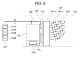
- Fig. 6 shows a front configuration of the power converter 10A in related art.
- the power converter 10A in related art is different from the power converter 10 in the embodiment in the following points.
- the power converter 10A in related art is different from the power converter 10 in the embodiment in that the power converter 10A is installed separately from an overvoltage protection device 18A within the same casing 1, the length of wiring between the overvoltage protection device 18A and a filter capacitor 12A is equal to or longer than a certain length because of separate installation and an induction voltage is generated in the parts and the induction voltage may be applied to a power switching element 182A provided in the overvoltage protection device 18A, and a snubber circuit 184A is provided within the overvoltage protection device 18A for protecting the power switching element 182A.
- Fig. 7 shows a perspective configuration of the power converter 10A in related art.
- the filter capacitor 12A, a cooling block 141A, and a cooling fin 142A are sequentially arranged from the front side to the depth side, and gate control circuits 16A are provided under the filter capacitor 12A, and input/output terminals 15A are provided in the cooling block 141A.
- the overvoltage protection device 18A is installed separately from the power converter 10A within the same casing 1.
- Fig. 8 shows a front configuration of a main part of the power converter 10A in related art.
- power switching elements 11A the filter capacitor 12A, a conductor bar 13A, the cooling block 141A, and the overvoltage protection device 18A are shown.
- the snubber circuit 184A is necessary for the overvoltage protection device 18A.
- the snubber circuit 184A includes a snubber resistor, a snubber diode, and a snubber capacitor as described above and the snubber capacitor is particularly heavy and bulky, and thereby, hinders reduction in weight and size of the casing 1 housing the overvoltage protection device 18A.
- the filter capacitor 12 and the overvoltage protection device 18 are provided closer to each other so that the conductor wiring length between the filter capacitor 12 and the overvoltage protection device 18 may be the shortest, and thereby, the inductance component of the conductor wiring between the filter capacitor 12 and the overvoltage protection device 18 may be reduced to the negligible level and the snubber circuit 184A may be eliminated.
- the reduction in weight and size of the overvoltage protection device 18 may be realized and the improvement in reliability of the power converter 10 may be realized.
- the conductor bar 13 having the thin flat plate shape is extended close to and along them, and thereby, further reduction in wiring inductance may be realized.
- the overvoltage protection device 18 may be directly attached and fixed to the power converter 10 so that the filter capacitor 12 and the overvoltage protection device 18 may be arranged closer to each other.
Landscapes
- Engineering & Computer Science (AREA)
- Mechanical Engineering (AREA)
- Transportation (AREA)
- Power Engineering (AREA)
- Microelectronics & Electronic Packaging (AREA)
- Sustainable Development (AREA)
- Sustainable Energy (AREA)
- Life Sciences & Earth Sciences (AREA)
- Automation & Control Theory (AREA)
- Physics & Mathematics (AREA)
- Thermal Sciences (AREA)
- Inverter Devices (AREA)
- Electric Propulsion And Braking For Vehicles (AREA)
Description
- The present invention relates to a power converter, and specifically, is preferably applied to a power converter for rolling stock.
- A power converter provided in rolling stock power-converts DC power input from a railroad wire using a plurality of power switching elements and outputs the power to a motor for rolling stock. The power converter mainly includes the power switching elements, a cooling unit for cooling the power switching elements, and a filter capacitor for stabilization of the DC power input from the railroad wire.
- Patent Document 1 (
JP-A-5-83957 - According to the power converter disclosed in Patent Document 1, connecting lines for connecting the units for three phases to one another may be made shorter, and high voltages applied to the power switching elements may be suppressed even when the capacities of the snubber circuits are smaller.
- However, the snubber circuit in the power converter disclosed in Patent Document 1 includes a snubber resistor, a snubber diode, and a snubber capacitor, and is heavy and bulky particularly because of the snubber capacitor. Accordingly, in the configuration disclosed in Patent Document 1, it is impossible to reduce the weight of the power converter.
- Further, the snubber circuits are heavy and bulky as described above, and necessary to be provided separately from the power switching elements within a casing that houses the power converter. When the snubber circuits are provided separately from the power switching element, the layout of the devices within the casing is restricted. Thus, it is impossible to downsize the power converter.
- Furthermore, when the snubber circuits and the power switching elements are separately provided, the wiring between them is longer and, if the wiring is equal to or longer than a certain length, the inductance component of the wiring is not negligible. In this case, an inductance voltage is generated in the wiring part and it is impossible to properly protect the power switching elements.
- The invention has been achieved in consideration of the above described points, and an object of the invention is to provide a power converter in which reduction in weight and size may be realized and improvement in reliability may be realized by properly protecting power switching elements.
- In order to solve the problem, a power converter for rolling stock in the invention includes a filter capacitor that smoothes a DC voltage, an overvoltage protection device that releases charge accumulated in the filter capacitor, a plurality of power switching elements that convert a DC voltage into an AC voltage, a cooling unit that cools the power switching elements, and a conductor bar that electrically connects the filter capacitor, the overvoltage protection device, and the power switching elements. The overvoltage protection device may be provided adjacent or closer to the filter capacitor.
- The length of the conductor bar between the overvoltage protection device and the filter capacitor may have a negligible (i.e. substantially zero) inductance.
- According to the invention, reduction in weight and size may be realized and improvement in reliability may be realized by properly protecting power switching elements.
-
-
Fig. 1 is an overall configuration diagram showing attachment positions of power converters. -
Fig. 2 is a front configuration diagram of the power converter. -
Fig. 3 is a perspective configuration diagram of the power converter. -
Fig. 4 is a front configuration diagram of a main part of the power converter. -
Fig. 5 is a circuit configuration diagram of the power converter. -
Fig. 6 is a front configuration diagram of a power converter in related art. -
Fig. 7 is a perspective configuration diagram of the power converter in related art. -
Fig. 8 is a front configuration diagram of a main part of the power converter in related art. - As below, one embodiment of the invention will be explained with reference to the drawings.
-
Fig. 1 shows attachment positions ofpower converters 10 in the embodiment. Thepower converter 10 is housed and installed inside of a casing 1 provided under the floor of rolling stock R. -
Fig. 2 shows a front configuration of thepower converter 10. Thepower converter 10 includespower switching elements 11, afilter capacitor 12, aconductor bar 13, acooling unit 14, input/output terminals 15, agate control circuit 16, agate wire 17, and anovervoltage protection device 18. - The
power converter 10 is a device that generates DC from single-phase AC and a device that generates three-phase AC from DC. The former is called a converter and the latter is called an inverter. - The converter converts a single-phase AC voltage from an AC power source into a DC voltage and charges the
filter capacitor 12 for DC voltage smoothing, and includes a two-phase leg. - The inverter converts the DC voltage charged in the
filter capacitor 12 into an AC voltage by continuously changing a ratio of ON/OFF of thepower switching elements 11, and includes a three-phase leg. - The
power converter 10 generates three-phase AC via the converter and the inverter, and thereby, drives a motor provided in the rolling stock R. Note that any power conversion is performed through a group of semiconductors. Further, for conduction control, a controller separately provided outputs control signals and drives thepower switching elements 11 via thegate control circuit 16 and thegate wire 17 mounted on thepower converter 10. - The
power switching element 11 is an IGBT (Insulated Gate Bipolar Transistor), for example. The IGBT has an advantage that the ON-resistance and the drive current are smaller and the switching speed is higher. On the other hand, the IGBT consumes high power at conduction and interruption and generates heat, and thecooling unit 14 is provided for heat dissipation in the embodiment. - The
filter capacitor 12 is for smoothing the DC voltage as described above. - The
conductor bar 13 is a connecting line having a flat plate shape for electrical connection to an external device, and also called a laminated bus bar. The laminated bus bar has a structure that suppresses an abnormal voltage (surge voltage) generated at high-speed switching in an electric circuit using thepower switching elements 11 such as an IGBT. - Specifically, as a material for the
conductor bar 13, copper having lower volume resistivity is used for suppression of heat generation of the conductor, and the conductor bar has a shape having larger conductor section area. Theconductor bar 13 has a thin flat plate shape so that the wiring inductance may be reduced. - The
cooling unit 14 includes acooling block 141, acooling fin 142, and aheat pipe 143. Thecooling block 141 absorbs heat generated from thepower switching elements 11 and gasifies a cooling medium enclosed in theheat pipe 143 for cooling. The coolingfin 142 blows air to the gasified cooling medium and liquefies the cooling medium again by heat exchange. Note that thecooling unit 14 in the embodiment employs the heat pipe system, however, may employ a radiator system. - The input/
output terminals 15 include DC terminals P and N for inputting DC and AC terminals U, V, and W for converting the DC input from the DC terminals P and N into three-phase AC at arbitrary frequencies and arbitrary voltages and outputting the AC. - The
gate control circuit 16 is a circuit for generating and outputting gate signals. Thegate wire 17 is a wire for outputting the gate signals generated and output from thegate control circuit 16 to thepower switching elements 11. - The
overvoltage protection device 18 includes aDC voltage detector 181, apower switching element 182, and adrive circuit 183. Theovervoltage protection device 18 is a device for turning ON thepower switching element 182 and releasing charge accumulated in thefilter capacitor 12 when an overvoltage of thefilter capacitor 12 is detected and when the control power source is turned OFF. TheDC voltage detector 181 detects the overvoltage of thefilter capacitor 12, thepower switching element 182 is switched to ON when the charge accumulated in thefilter capacitor 12 is released, and thedrive circuit 183 switches ON/OFF by driving thepower switching element 182. - Note that an overvoltage protection device in related art includes a snubber circuit in addition to the above described configuration. The snubber circuit is a circuit that commutates energy accumulated in the inductance component of the wiring to a snubber capacitor for suppressing a surge voltage generated when the
power switching element 182 is turned OFF, and includes a snubber resistor, a snubber diode, and the snubber capacitor. - In the embodiment, the
overvoltage protection device 18 formed by eliminating the snubber circuit from the overvoltage protection device in related art is employed for realization of reduction in weight and size. - Here, as described above, the snubber circuit is the circuit for suppressing the surge voltage and, when the snubber circuit is eliminated, suppression of the surge voltage is harder. However, in the embodiment, the
overvoltage protection device 18 is provided closer to thefilter capacitor 12 so that the length of the wiring (conductor bar 13) between theovervoltage protection device 18 and thefilter capacitor 12 may be as short as possible. Thus, the inductance of the wiring is negligible and generation of the surge voltage may be suppressed. -
Fig. 3 shows a perspective configuration of thepower converter 10. The perspective configuration shown inFig. 3 is a perspective configuration as seen from a direction D1 shown inFig. 2 . In thepower converter 10, theovervoltage protection device 18, thefilter capacitor 12, thecooling block 141, and the coolingfin 142 are sequentially arranged from the front side to the depth side, and the input/output terminals 15 are provided in thecooling block 141. These are housed within the same casing 1 as thepower converter 10. -
Fig. 4 shows a front configuration of a main part of thepower converter 10. Here, of thepower converter 10 shown inFig. 2 , particularly, thepower switching elements 11, thefilter capacitor 12, theconductor bar 13, thecooling block 141, and theovervoltage protection device 18 are shown. - The
filter capacitor 12 and theovervoltage protection device 18 are arranged to be closer to each other so that terminals respectively provided may be in the same direction. Theconductor bar 13 is provided to extend along the upper surfaces of thefilter capacitor 12 and theovervoltage protection device 18 and to respectively connect thepower switching elements 11, thefilter capacitor 12, and theovervoltage protection device 18. - In the embodiment, the arrangement configuration in which physical distances L1 and L2 between the
filter capacitor 12 and theovervoltage protection device 18 are as short as possible is employed, and, even when the snubber circuit is eliminated from theovervoltage protection device 18, generation of an induction voltage in the parts may be suppressed. -
Fig. 5 shows a circuit configuration of thepower converter 10. The feeding system for railroad includes an AC system and a DC system, and the motor includes an AC motor and a DC motor. Accordingly, depending on the combination of the feeding system and the motor, thepower converter 10 may include a single inverter system, a single converter system, and a combination of them. In the embodiment, an inverter applied to the case of a combination of the DC feeding system and the AC motor will be explained as an example. - The main circuit of the
power converter 10 in the embodiment includes thefilter capacitor 12 connected between the DC terminals P and N of the input/output terminals 15, and a three-phase inverter. The three-phase inverter converts the input DC into three-phase AC at arbitrary frequencies and arbitrary voltages and outputs the three-phase AC to the AC terminals U, V, and W of the input/output terminals 15. - The three-phase inverter includes six of the
power switching elements 11. Thepower switching element 11 for each phase includes an element and a free wheel diode parallel-connected to the element. - In the embodiment, the lengths L1 and L2 of the wiring between the
filter capacitor 12 and theovervoltage protection device 18 is made as short as possible, and generation of an induction voltage in the L1 and L2 parts may be suppressed. - As below, a
power converter 10A in related art will be explained with reference toFigs. 6 to 8 . The same configurations as those of thepower converter 10 in the embodiment have the same signs or the same signs with A and their explanation will be omitted, and the different configurations will be explained. -
Fig. 6 shows a front configuration of thepower converter 10A in related art. Thepower converter 10A in related art is different from thepower converter 10 in the embodiment in the following points. - That is, the
power converter 10A in related art is different from thepower converter 10 in the embodiment in that thepower converter 10A is installed separately from anovervoltage protection device 18A within the same casing 1, the length of wiring between theovervoltage protection device 18A and afilter capacitor 12A is equal to or longer than a certain length because of separate installation and an induction voltage is generated in the parts and the induction voltage may be applied to apower switching element 182A provided in theovervoltage protection device 18A, and asnubber circuit 184A is provided within theovervoltage protection device 18A for protecting thepower switching element 182A. -
Fig. 7 shows a perspective configuration of thepower converter 10A in related art. In thepower converter 10A, thefilter capacitor 12A, acooling block 141A, and acooling fin 142A are sequentially arranged from the front side to the depth side, andgate control circuits 16A are provided under thefilter capacitor 12A, and input/output terminals 15A are provided in thecooling block 141A. These are housed within the same casing 1 as thepower converter 10A. Further, theovervoltage protection device 18A is installed separately from thepower converter 10A within the same casing 1. -
Fig. 8 shows a front configuration of a main part of thepower converter 10A in related art. Here, of thepower converter 10A shown inFig. 6 , particularly,power switching elements 11A, thefilter capacitor 12A, aconductor bar 13A, thecooling block 141A, and theovervoltage protection device 18A are shown. - In the embodiment in related art, physical distances L11 and L12 between the
filter capacitor 12A and theovervoltage protection device 18A are longer and an inductance voltage is generated in the parts. Accordingly, in order to protect thepower switching element 182A from the induction voltage, thesnubber circuit 184A is necessary for theovervoltage protection device 18A. Thesnubber circuit 184A includes a snubber resistor, a snubber diode, and a snubber capacitor as described above and the snubber capacitor is particularly heavy and bulky, and thereby, hinders reduction in weight and size of the casing 1 housing theovervoltage protection device 18A. - As described above, according to the embodiment, the
filter capacitor 12 and theovervoltage protection device 18 are provided closer to each other so that the conductor wiring length between thefilter capacitor 12 and theovervoltage protection device 18 may be the shortest, and thereby, the inductance component of the conductor wiring between thefilter capacitor 12 and theovervoltage protection device 18 may be reduced to the negligible level and thesnubber circuit 184A may be eliminated. Thus, the reduction in weight and size of theovervoltage protection device 18 may be realized and the improvement in reliability of thepower converter 10 may be realized. - Further, for the connection between the
filter capacitor 12 and theovervoltage protection device 18, theconductor bar 13 having the thin flat plate shape is extended close to and along them, and thereby, further reduction in wiring inductance may be realized. - Furthermore, with the reduction in weight of the
overvoltage protection device 18, theovervoltage protection device 18 may be directly attached and fixed to thepower converter 10 so that thefilter capacitor 12 and theovervoltage protection device 18 may be arranged closer to each other.
Claims (6)
- A power converter for rolling stock comprising:a filter capacitor that smoothes a DC voltage;an overvoltage protection device that releases charge accumulated in the filter capacitor;a plurality of power switching elements that convert a DC voltage into an AC voltage;a cooling unit that cools the power switching elements; anda conductor bar that electrically connects the filter capacitor, the overvoltage protection device, and the power switching elements,wherein the overvoltage protection device is provided adjacent to the filter capacitor.
- The power converter according to claim 1, wherein the overvoltage protection device is fixed so that a condition that the device is provided closer to the filter capacitor may be maintained.
- The power converter according to claim 1 or 2, wherein the overvoltage protection device is directly attached and fixed to the power converter.
- The power converter according to any one of claims 1 to 3, wherein the overvoltage protection device includes:a DC voltage detector that detects a voltage accumulated in the filter capacitor;a power switching element for overvoltage protection device switched to ON when the charge accumulated in the filter capacitor is released; anda drive circuit that controls drive of the power switching element for overvoltage protection device.
- The power converter according to any one of claims 1 to 4, wherein the conductor bar has a thin flat plate shape, is provided to extend over between the filter capacitor and the overvoltage protection device, and connects the filter capacitor and the overvoltage protection device.
- The power converter according to claim 5, wherein a terminal of the filter capacitor and a terminal of the overvoltage protection device connected to the conductor bar are respectively provided at the same side with that of the power converter.
Applications Claiming Priority (1)
| Application Number | Priority Date | Filing Date | Title |
|---|---|---|---|
| JP2013176323A JP6182021B2 (en) | 2013-08-28 | 2013-08-28 | Power converter |
Publications (3)
| Publication Number | Publication Date |
|---|---|
| EP2842791A2 true EP2842791A2 (en) | 2015-03-04 |
| EP2842791A3 EP2842791A3 (en) | 2015-09-16 |
| EP2842791B1 EP2842791B1 (en) | 2021-08-25 |
Family
ID=51229841
Family Applications (1)
| Application Number | Title | Priority Date | Filing Date |
|---|---|---|---|
| EP14179244.0A Active EP2842791B1 (en) | 2013-08-28 | 2014-07-31 | Power converter |
Country Status (4)
| Country | Link |
|---|---|
| EP (1) | EP2842791B1 (en) |
| JP (1) | JP6182021B2 (en) |
| KR (1) | KR101600186B1 (en) |
| CN (1) | CN104426385B (en) |
Cited By (3)
| Publication number | Priority date | Publication date | Assignee | Title |
|---|---|---|---|---|
| US11736034B2 (en) | 2019-04-01 | 2023-08-22 | Mitsubishi Electric Corporation | Power conversion device |
| DE102016207639B4 (en) | 2015-05-07 | 2025-05-28 | Hitachi, Ltd. | Power converter and railway vehicle |
| DE102016207701B4 (en) | 2015-05-07 | 2025-07-17 | Hitachi, Ltd. | Power converters and rail vehicles |
Families Citing this family (2)
| Publication number | Priority date | Publication date | Assignee | Title |
|---|---|---|---|---|
| JP5778840B1 (en) * | 2014-09-25 | 2015-09-16 | 株式会社日立製作所 | Power conversion unit and power conversion device |
| JP6529868B2 (en) * | 2015-09-09 | 2019-06-12 | 株式会社東芝 | Electric car control device |
Citations (1)
| Publication number | Priority date | Publication date | Assignee | Title |
|---|---|---|---|---|
| JPS583957A (en) | 1981-06-27 | 1983-01-10 | Nisshin Steel Co Ltd | Zinc hot dipping device |
Family Cites Families (14)
| Publication number | Priority date | Publication date | Assignee | Title |
|---|---|---|---|---|
| JPS60200703A (en) * | 1984-03-26 | 1985-10-11 | Hitachi Ltd | Controller of ac electric railcar |
| JPH0583957A (en) * | 1991-09-18 | 1993-04-02 | Hitachi Ltd | Power converter |
| JPH0937414A (en) * | 1995-07-20 | 1997-02-07 | Mitsubishi Electric Corp | Inverter device for electric vehicles |
| JP3263316B2 (en) * | 1996-06-28 | 2002-03-04 | 株式会社日立製作所 | Electric vehicle control device |
| JPH1098887A (en) * | 1996-09-20 | 1998-04-14 | Hitachi Ltd | Power converter |
| US6160696A (en) * | 1998-05-04 | 2000-12-12 | General Electric Company | Modular bus bar and switch assembly for traction inverter |
| JP3046276B2 (en) * | 1998-05-11 | 2000-05-29 | 三菱電機株式会社 | Power converter |
| KR100485102B1 (en) * | 2002-09-17 | 2005-04-20 | 주식회사 플라스포 | Inverter stack having multi-layer bus plate |
| JP4356434B2 (en) * | 2003-11-27 | 2009-11-04 | 富士電機システムズ株式会社 | 3-level inverter circuit |
| EP2034601A1 (en) * | 2006-06-27 | 2009-03-11 | Mitsubishi Electric Corporation | Power converter |
| JP5367444B2 (en) * | 2009-04-28 | 2013-12-11 | 株式会社東芝 | Electric vehicle control device and test method thereof |
| EP2514626B1 (en) * | 2009-12-18 | 2019-04-24 | Mitsubishi Electric Corporation | Electric vehicle drive control apparatus |
| WO2011125784A1 (en) * | 2010-03-31 | 2011-10-13 | 株式会社 東芝 | Electric vehicle control device |
| EP2506421B1 (en) * | 2011-03-31 | 2020-07-08 | Kabushiki Kaisha Toshiba | Electric vehicle control device |
-
2013
- 2013-08-28 JP JP2013176323A patent/JP6182021B2/en active Active
-
2014
- 2014-07-31 EP EP14179244.0A patent/EP2842791B1/en active Active
- 2014-08-01 KR KR1020140098989A patent/KR101600186B1/en active Active
- 2014-08-01 CN CN201410377271.9A patent/CN104426385B/en active Active
Patent Citations (1)
| Publication number | Priority date | Publication date | Assignee | Title |
|---|---|---|---|---|
| JPS583957A (en) | 1981-06-27 | 1983-01-10 | Nisshin Steel Co Ltd | Zinc hot dipping device |
Cited By (3)
| Publication number | Priority date | Publication date | Assignee | Title |
|---|---|---|---|---|
| DE102016207639B4 (en) | 2015-05-07 | 2025-05-28 | Hitachi, Ltd. | Power converter and railway vehicle |
| DE102016207701B4 (en) | 2015-05-07 | 2025-07-17 | Hitachi, Ltd. | Power converters and rail vehicles |
| US11736034B2 (en) | 2019-04-01 | 2023-08-22 | Mitsubishi Electric Corporation | Power conversion device |
Also Published As
| Publication number | Publication date |
|---|---|
| CN104426385A (en) | 2015-03-18 |
| KR20150026810A (en) | 2015-03-11 |
| CN104426385B (en) | 2017-10-03 |
| EP2842791B1 (en) | 2021-08-25 |
| JP6182021B2 (en) | 2017-08-16 |
| KR101600186B1 (en) | 2016-03-04 |
| JP2015046993A (en) | 2015-03-12 |
| EP2842791A3 (en) | 2015-09-16 |
Similar Documents
| Publication | Publication Date | Title |
|---|---|---|
| US10404156B2 (en) | Power converter | |
| CN104054245B (en) | Power conversion device | |
| CN110710341B (en) | Power phase modules for converters, converters and vehicles | |
| JP6373702B2 (en) | Semiconductor power module and semiconductor drive device | |
| EP2842791B1 (en) | Power converter | |
| JPWO2019026339A1 (en) | Power converter and vehicle equipped with the power converter | |
| JP6812317B2 (en) | Vehicles equipped with power converters and power converters | |
| CN103650316A (en) | Power conversion device | |
| EP3745579B1 (en) | Power conversion device and electric railroad vehicle equipped with power conversion device | |
| CN103597726A (en) | Power converter | |
| CN103597728A (en) | Power conversion device | |
| JP4765017B2 (en) | AC-AC power converter | |
| CN107624217A (en) | Power inverter | |
| TWI590570B (en) | Power conversion device and vehicle control device | |
| JP7167328B2 (en) | power converter | |
| JP6720601B2 (en) | Power converter | |
| JP4735109B2 (en) | Matrix converter device | |
| JP6906431B2 (en) | Flow reducer | |
| JP6713246B2 (en) | Power converter | |
| JP6568422B2 (en) | Power converter | |
| JP4424918B2 (en) | Power converter | |
| JP6433579B2 (en) | Power converter | |
| EP4075932A1 (en) | Power conversion device |
Legal Events
| Date | Code | Title | Description |
|---|---|---|---|
| 17P | Request for examination filed |
Effective date: 20140818 |
|
| AK | Designated contracting states |
Kind code of ref document: A2 Designated state(s): AL AT BE BG CH CY CZ DE DK EE ES FI FR GB GR HR HU IE IS IT LI LT LU LV MC MK MT NL NO PL PT RO RS SE SI SK SM TR |
|
| AX | Request for extension of the european patent |
Extension state: BA ME |
|
| PUAI | Public reference made under article 153(3) epc to a published international application that has entered the european phase |
Free format text: ORIGINAL CODE: 0009012 |
|
| PUAL | Search report despatched |
Free format text: ORIGINAL CODE: 0009013 |
|
| AK | Designated contracting states |
Kind code of ref document: A3 Designated state(s): AL AT BE BG CH CY CZ DE DK EE ES FI FR GB GR HR HU IE IS IT LI LT LU LV MC MK MT NL NO PL PT RO RS SE SI SK SM TR |
|
| AX | Request for extension of the european patent |
Extension state: BA ME |
|
| RIC1 | Information provided on ipc code assigned before grant |
Ipc: B60L 9/04 20060101AFI20150810BHEP Ipc: B60L 9/18 20060101ALI20150810BHEP |
|
| STAA | Information on the status of an ep patent application or granted ep patent |
Free format text: STATUS: EXAMINATION IS IN PROGRESS |
|
| 17Q | First examination report despatched |
Effective date: 20181126 |
|
| REG | Reference to a national code |
Ref country code: DE Ref legal event code: R079 Ref document number: 602014079637 Country of ref document: DE Free format text: PREVIOUS MAIN CLASS: B60L0009040000 Ipc: B61C0017000000 |
|
| RIC1 | Information provided on ipc code assigned before grant |
Ipc: H05K 7/00 20060101ALI20210215BHEP Ipc: B61C 17/00 20060101AFI20210215BHEP |
|
| GRAP | Despatch of communication of intention to grant a patent |
Free format text: ORIGINAL CODE: EPIDOSNIGR1 |
|
| STAA | Information on the status of an ep patent application or granted ep patent |
Free format text: STATUS: GRANT OF PATENT IS INTENDED |
|
| INTG | Intention to grant announced |
Effective date: 20210326 |
|
| GRAS | Grant fee paid |
Free format text: ORIGINAL CODE: EPIDOSNIGR3 |
|
| GRAA | (expected) grant |
Free format text: ORIGINAL CODE: 0009210 |
|
| STAA | Information on the status of an ep patent application or granted ep patent |
Free format text: STATUS: THE PATENT HAS BEEN GRANTED |
|
| AK | Designated contracting states |
Kind code of ref document: B1 Designated state(s): AL AT BE BG CH CY CZ DE DK EE ES FI FR GB GR HR HU IE IS IT LI LT LU LV MC MK MT NL NO PL PT RO RS SE SI SK SM TR |
|
| REG | Reference to a national code |
Ref country code: GB Ref legal event code: FG4D |
|
| REG | Reference to a national code |
Ref country code: CH Ref legal event code: EP |
|
| REG | Reference to a national code |
Ref country code: IE Ref legal event code: FG4D Ref country code: AT Ref legal event code: REF Ref document number: 1423509 Country of ref document: AT Kind code of ref document: T Effective date: 20210915 |
|
| REG | Reference to a national code |
Ref country code: DE Ref legal event code: R096 Ref document number: 602014079637 Country of ref document: DE |
|
| REG | Reference to a national code |
Ref country code: LT Ref legal event code: MG9D |
|
| REG | Reference to a national code |
Ref country code: NL Ref legal event code: MP Effective date: 20210825 |
|
| REG | Reference to a national code |
Ref country code: AT Ref legal event code: MK05 Ref document number: 1423509 Country of ref document: AT Kind code of ref document: T Effective date: 20210825 |
|
| PG25 | Lapsed in a contracting state [announced via postgrant information from national office to epo] |
Ref country code: NO Free format text: LAPSE BECAUSE OF FAILURE TO SUBMIT A TRANSLATION OF THE DESCRIPTION OR TO PAY THE FEE WITHIN THE PRESCRIBED TIME-LIMIT Effective date: 20211125 Ref country code: PT Free format text: LAPSE BECAUSE OF FAILURE TO SUBMIT A TRANSLATION OF THE DESCRIPTION OR TO PAY THE FEE WITHIN THE PRESCRIBED TIME-LIMIT Effective date: 20211227 Ref country code: FI Free format text: LAPSE BECAUSE OF FAILURE TO SUBMIT A TRANSLATION OF THE DESCRIPTION OR TO PAY THE FEE WITHIN THE PRESCRIBED TIME-LIMIT Effective date: 20210825 Ref country code: ES Free format text: LAPSE BECAUSE OF FAILURE TO SUBMIT A TRANSLATION OF THE DESCRIPTION OR TO PAY THE FEE WITHIN THE PRESCRIBED TIME-LIMIT Effective date: 20210825 Ref country code: LT Free format text: LAPSE BECAUSE OF FAILURE TO SUBMIT A TRANSLATION OF THE DESCRIPTION OR TO PAY THE FEE WITHIN THE PRESCRIBED TIME-LIMIT Effective date: 20210825 Ref country code: BG Free format text: LAPSE BECAUSE OF FAILURE TO SUBMIT A TRANSLATION OF THE DESCRIPTION OR TO PAY THE FEE WITHIN THE PRESCRIBED TIME-LIMIT Effective date: 20211125 Ref country code: AT Free format text: LAPSE BECAUSE OF FAILURE TO SUBMIT A TRANSLATION OF THE DESCRIPTION OR TO PAY THE FEE WITHIN THE PRESCRIBED TIME-LIMIT Effective date: 20210825 Ref country code: RS Free format text: LAPSE BECAUSE OF FAILURE TO SUBMIT A TRANSLATION OF THE DESCRIPTION OR TO PAY THE FEE WITHIN THE PRESCRIBED TIME-LIMIT Effective date: 20210825 Ref country code: SE Free format text: LAPSE BECAUSE OF FAILURE TO SUBMIT A TRANSLATION OF THE DESCRIPTION OR TO PAY THE FEE WITHIN THE PRESCRIBED TIME-LIMIT Effective date: 20210825 Ref country code: HR Free format text: LAPSE BECAUSE OF FAILURE TO SUBMIT A TRANSLATION OF THE DESCRIPTION OR TO PAY THE FEE WITHIN THE PRESCRIBED TIME-LIMIT Effective date: 20210825 |
|
| PG25 | Lapsed in a contracting state [announced via postgrant information from national office to epo] |
Ref country code: PL Free format text: LAPSE BECAUSE OF FAILURE TO SUBMIT A TRANSLATION OF THE DESCRIPTION OR TO PAY THE FEE WITHIN THE PRESCRIBED TIME-LIMIT Effective date: 20210825 Ref country code: LV Free format text: LAPSE BECAUSE OF FAILURE TO SUBMIT A TRANSLATION OF THE DESCRIPTION OR TO PAY THE FEE WITHIN THE PRESCRIBED TIME-LIMIT Effective date: 20210825 Ref country code: GR Free format text: LAPSE BECAUSE OF FAILURE TO SUBMIT A TRANSLATION OF THE DESCRIPTION OR TO PAY THE FEE WITHIN THE PRESCRIBED TIME-LIMIT Effective date: 20211126 |
|
| PG25 | Lapsed in a contracting state [announced via postgrant information from national office to epo] |
Ref country code: NL Free format text: LAPSE BECAUSE OF FAILURE TO SUBMIT A TRANSLATION OF THE DESCRIPTION OR TO PAY THE FEE WITHIN THE PRESCRIBED TIME-LIMIT Effective date: 20210825 |
|
| PG25 | Lapsed in a contracting state [announced via postgrant information from national office to epo] |
Ref country code: DK Free format text: LAPSE BECAUSE OF FAILURE TO SUBMIT A TRANSLATION OF THE DESCRIPTION OR TO PAY THE FEE WITHIN THE PRESCRIBED TIME-LIMIT Effective date: 20210825 |
|
| REG | Reference to a national code |
Ref country code: DE Ref legal event code: R097 Ref document number: 602014079637 Country of ref document: DE |
|
| PG25 | Lapsed in a contracting state [announced via postgrant information from national office to epo] |
Ref country code: SM Free format text: LAPSE BECAUSE OF FAILURE TO SUBMIT A TRANSLATION OF THE DESCRIPTION OR TO PAY THE FEE WITHIN THE PRESCRIBED TIME-LIMIT Effective date: 20210825 Ref country code: SK Free format text: LAPSE BECAUSE OF FAILURE TO SUBMIT A TRANSLATION OF THE DESCRIPTION OR TO PAY THE FEE WITHIN THE PRESCRIBED TIME-LIMIT Effective date: 20210825 Ref country code: RO Free format text: LAPSE BECAUSE OF FAILURE TO SUBMIT A TRANSLATION OF THE DESCRIPTION OR TO PAY THE FEE WITHIN THE PRESCRIBED TIME-LIMIT Effective date: 20210825 Ref country code: EE Free format text: LAPSE BECAUSE OF FAILURE TO SUBMIT A TRANSLATION OF THE DESCRIPTION OR TO PAY THE FEE WITHIN THE PRESCRIBED TIME-LIMIT Effective date: 20210825 Ref country code: CZ Free format text: LAPSE BECAUSE OF FAILURE TO SUBMIT A TRANSLATION OF THE DESCRIPTION OR TO PAY THE FEE WITHIN THE PRESCRIBED TIME-LIMIT Effective date: 20210825 Ref country code: AL Free format text: LAPSE BECAUSE OF FAILURE TO SUBMIT A TRANSLATION OF THE DESCRIPTION OR TO PAY THE FEE WITHIN THE PRESCRIBED TIME-LIMIT Effective date: 20210825 |
|
| PLBE | No opposition filed within time limit |
Free format text: ORIGINAL CODE: 0009261 |
|
| STAA | Information on the status of an ep patent application or granted ep patent |
Free format text: STATUS: NO OPPOSITION FILED WITHIN TIME LIMIT |
|
| 26N | No opposition filed |
Effective date: 20220527 |
|
| PG25 | Lapsed in a contracting state [announced via postgrant information from national office to epo] |
Ref country code: SI Free format text: LAPSE BECAUSE OF FAILURE TO SUBMIT A TRANSLATION OF THE DESCRIPTION OR TO PAY THE FEE WITHIN THE PRESCRIBED TIME-LIMIT Effective date: 20210825 |
|
| PG25 | Lapsed in a contracting state [announced via postgrant information from national office to epo] |
Ref country code: MC Free format text: LAPSE BECAUSE OF FAILURE TO SUBMIT A TRANSLATION OF THE DESCRIPTION OR TO PAY THE FEE WITHIN THE PRESCRIBED TIME-LIMIT Effective date: 20210825 |
|
| REG | Reference to a national code |
Ref country code: CH Ref legal event code: PL |
|
| REG | Reference to a national code |
Ref country code: BE Ref legal event code: MM Effective date: 20220731 |
|
| PG25 | Lapsed in a contracting state [announced via postgrant information from national office to epo] |
Ref country code: LU Free format text: LAPSE BECAUSE OF NON-PAYMENT OF DUE FEES Effective date: 20220731 Ref country code: LI Free format text: LAPSE BECAUSE OF NON-PAYMENT OF DUE FEES Effective date: 20220731 Ref country code: FR Free format text: LAPSE BECAUSE OF NON-PAYMENT OF DUE FEES Effective date: 20220731 Ref country code: CH Free format text: LAPSE BECAUSE OF NON-PAYMENT OF DUE FEES Effective date: 20220731 |
|
| PG25 | Lapsed in a contracting state [announced via postgrant information from national office to epo] |
Ref country code: BE Free format text: LAPSE BECAUSE OF NON-PAYMENT OF DUE FEES Effective date: 20220731 |
|
| PG25 | Lapsed in a contracting state [announced via postgrant information from national office to epo] |
Ref country code: IE Free format text: LAPSE BECAUSE OF NON-PAYMENT OF DUE FEES Effective date: 20220731 |
|
| PG25 | Lapsed in a contracting state [announced via postgrant information from national office to epo] |
Ref country code: HU Free format text: LAPSE BECAUSE OF FAILURE TO SUBMIT A TRANSLATION OF THE DESCRIPTION OR TO PAY THE FEE WITHIN THE PRESCRIBED TIME-LIMIT; INVALID AB INITIO Effective date: 20140731 |
|
| PG25 | Lapsed in a contracting state [announced via postgrant information from national office to epo] |
Ref country code: MK Free format text: LAPSE BECAUSE OF FAILURE TO SUBMIT A TRANSLATION OF THE DESCRIPTION OR TO PAY THE FEE WITHIN THE PRESCRIBED TIME-LIMIT Effective date: 20210825 Ref country code: CY Free format text: LAPSE BECAUSE OF FAILURE TO SUBMIT A TRANSLATION OF THE DESCRIPTION OR TO PAY THE FEE WITHIN THE PRESCRIBED TIME-LIMIT Effective date: 20210825 |
|
| PG25 | Lapsed in a contracting state [announced via postgrant information from national office to epo] |
Ref country code: TR Free format text: LAPSE BECAUSE OF FAILURE TO SUBMIT A TRANSLATION OF THE DESCRIPTION OR TO PAY THE FEE WITHIN THE PRESCRIBED TIME-LIMIT Effective date: 20210825 |
|
| PG25 | Lapsed in a contracting state [announced via postgrant information from national office to epo] |
Ref country code: MT Free format text: LAPSE BECAUSE OF FAILURE TO SUBMIT A TRANSLATION OF THE DESCRIPTION OR TO PAY THE FEE WITHIN THE PRESCRIBED TIME-LIMIT Effective date: 20210825 |
|
| PGFP | Annual fee paid to national office [announced via postgrant information from national office to epo] |
Ref country code: GB Payment date: 20250612 Year of fee payment: 12 |
|
| PGFP | Annual fee paid to national office [announced via postgrant information from national office to epo] |
Ref country code: DE Payment date: 20250604 Year of fee payment: 12 |
|
| PGFP | Annual fee paid to national office [announced via postgrant information from national office to epo] |
Ref country code: IT Payment date: 20250623 Year of fee payment: 12 |