EP2837173B1 - Infrared detector with increased image resolution - Google Patents
Infrared detector with increased image resolution Download PDFInfo
- Publication number
- EP2837173B1 EP2837173B1 EP13729475.7A EP13729475A EP2837173B1 EP 2837173 B1 EP2837173 B1 EP 2837173B1 EP 13729475 A EP13729475 A EP 13729475A EP 2837173 B1 EP2837173 B1 EP 2837173B1
- Authority
- EP
- European Patent Office
- Prior art keywords
- detector
- detector array
- image
- pixel
- fill factor
- Prior art date
- Legal status (The legal status is an assumption and is not a legal conclusion. Google has not performed a legal analysis and makes no representation as to the accuracy of the status listed.)
- Active
Links
- 238000003384 imaging method Methods 0.000 claims description 80
- 230000000873 masking effect Effects 0.000 claims description 69
- 238000000034 method Methods 0.000 claims description 51
- 230000003287 optical effect Effects 0.000 claims description 28
- 230000035945 sensitivity Effects 0.000 claims description 15
- 238000003331 infrared imaging Methods 0.000 claims description 10
- 239000011159 matrix material Substances 0.000 claims description 10
- 239000011248 coating agent Substances 0.000 claims description 3
- 238000000576 coating method Methods 0.000 claims description 3
- 238000001931 thermography Methods 0.000 claims description 3
- 230000005855 radiation Effects 0.000 description 20
- 239000011295 pitch Substances 0.000 description 4
- 238000003491 array Methods 0.000 description 3
- 230000003247 decreasing effect Effects 0.000 description 3
- 238000013461 design Methods 0.000 description 3
- 238000005070 sampling Methods 0.000 description 3
- 238000012546 transfer Methods 0.000 description 3
- 238000006073 displacement reaction Methods 0.000 description 2
- 230000000694 effects Effects 0.000 description 2
- 210000003128 head Anatomy 0.000 description 2
- 238000005057 refrigeration Methods 0.000 description 2
- 238000012935 Averaging Methods 0.000 description 1
- 241000698776 Duma Species 0.000 description 1
- 238000013459 approach Methods 0.000 description 1
- 230000000903 blocking effect Effects 0.000 description 1
- 210000000988 bone and bone Anatomy 0.000 description 1
- 230000000295 complement effect Effects 0.000 description 1
- 238000001816 cooling Methods 0.000 description 1
- 238000010438 heat treatment Methods 0.000 description 1
- 238000005286 illumination Methods 0.000 description 1
- 239000004973 liquid crystal related substance Substances 0.000 description 1
- 238000004519 manufacturing process Methods 0.000 description 1
- 239000000463 material Substances 0.000 description 1
- 239000002184 metal Substances 0.000 description 1
- 238000012634 optical imaging Methods 0.000 description 1
- 238000012545 processing Methods 0.000 description 1
- 210000001747 pupil Anatomy 0.000 description 1
- 239000004065 semiconductor Substances 0.000 description 1
- 238000001228 spectrum Methods 0.000 description 1
- 239000000126 substance Substances 0.000 description 1
Images

Classifications
-
- H—ELECTRICITY
- H04—ELECTRIC COMMUNICATION TECHNIQUE
- H04N—PICTORIAL COMMUNICATION, e.g. TELEVISION
- H04N5/00—Details of television systems
- H04N5/30—Transforming light or analogous information into electric information
- H04N5/33—Transforming infrared radiation
-
- G—PHYSICS
- G01—MEASURING; TESTING
- G01J—MEASUREMENT OF INTENSITY, VELOCITY, SPECTRAL CONTENT, POLARISATION, PHASE OR PULSE CHARACTERISTICS OF INFRARED, VISIBLE OR ULTRAVIOLET LIGHT; COLORIMETRY; RADIATION PYROMETRY
- G01J5/00—Radiation pyrometry, e.g. infrared or optical thermometry
- G01J5/02—Constructional details
- G01J5/06—Arrangements for eliminating effects of disturbing radiation; Arrangements for compensating changes in sensitivity
- G01J5/061—Arrangements for eliminating effects of disturbing radiation; Arrangements for compensating changes in sensitivity by controlling the temperature of the apparatus or parts thereof, e.g. using cooling means or thermostats
-
- G—PHYSICS
- G01—MEASURING; TESTING
- G01J—MEASUREMENT OF INTENSITY, VELOCITY, SPECTRAL CONTENT, POLARISATION, PHASE OR PULSE CHARACTERISTICS OF INFRARED, VISIBLE OR ULTRAVIOLET LIGHT; COLORIMETRY; RADIATION PYROMETRY
- G01J5/00—Radiation pyrometry, e.g. infrared or optical thermometry
- G01J5/02—Constructional details
- G01J5/08—Optical arrangements
- G01J5/0831—Masks; Aperture plates; Spatial light modulators
-
- H—ELECTRICITY
- H04—ELECTRIC COMMUNICATION TECHNIQUE
- H04N—PICTORIAL COMMUNICATION, e.g. TELEVISION
- H04N23/00—Cameras or camera modules comprising electronic image sensors; Control thereof
- H04N23/10—Cameras or camera modules comprising electronic image sensors; Control thereof for generating image signals from different wavelengths
- H04N23/11—Cameras or camera modules comprising electronic image sensors; Control thereof for generating image signals from different wavelengths for generating image signals from visible and infrared light wavelengths
-
- H—ELECTRICITY
- H04—ELECTRIC COMMUNICATION TECHNIQUE
- H04N—PICTORIAL COMMUNICATION, e.g. TELEVISION
- H04N25/00—Circuitry of solid-state image sensors [SSIS]; Control thereof
- H04N25/48—Increasing resolution by shifting the sensor relative to the scene
-
- G—PHYSICS
- G01—MEASURING; TESTING
- G01J—MEASUREMENT OF INTENSITY, VELOCITY, SPECTRAL CONTENT, POLARISATION, PHASE OR PULSE CHARACTERISTICS OF INFRARED, VISIBLE OR ULTRAVIOLET LIGHT; COLORIMETRY; RADIATION PYROMETRY
- G01J5/00—Radiation pyrometry, e.g. infrared or optical thermometry
- G01J2005/0077—Imaging
Definitions
- the disclosed technique generally relates to infrared image detectors having a two-dimensional sensor array, and to image resolution enhancement.
- CMOS complementary metal-oxide-semiconductor
- CCD charge-coupled device
- U.K. Patent No. 2,270,230 to Hirose entitled “Two dimensional image detector” discloses masking the pixels of a sensor array such that a subdivided region is imaged by each pixel.
- a mask is provided in opposition to a surface of the sensor array, where the mask includes windows having a smaller area than the array pixels.
- a mask shifter changes the positions of the windows at pitches smaller than those between the pixels.
- Light passing through the mask window and into each pixel in the sensor array is divided into a desired number of subdivisions as the mask changes position, thus increasing the spatial resolution of the image relative to the pixel size.
- the mask may be implemented via a metal mask or via electronic manipulation of a substance having polarizing characteristics, such as liquid crystals.
- European Patent No. 1,198,119 to Parsons entitled “Improved resolution for an electric image sensor array”, discloses introducing a partially occluding mask/light source between the sensor array and the image. Resolution improvement is obtained by displacement between the array and the mask/light source and calculating grey scale values for the improved resolution from the different changes in the charges of the individual array sensors.
- U.S. Patent No. 5,712,685 to Dumas entitled “Device to enhance imaging resolution”, is directed to improving resolution of a Focal Plane Array (FPA) image sensor with microscanning methodology.
- FPA Focal Plane Array
- a mask having a checkerboard pattern of opaque and transparent areas is located in front of and adjacent to the FPA onto which an image of a scene is optically focused.
- the mask and FPA are displaced with respect to each other in a number of micro-steps that extend in the same direction as the columns/rows of the FPA grid.
- the micro-steps are of equal lengths and are each a fraction of the length of a detector element.
- Opaque areas of the mask progressively cover equal areas of detector elements in discrete steps for each micro-step movement in one direction at the same time as transparent areas of the mask progressively uncover equal areas of other detector elements for each discrete step.
- Outputs from the detector elements provide signals for sample slices of the scene for each micro-step, and an image of the scene is reconstructed from the signals.
- this article introduces the sampling-averaging MTF of a detector array at a spatial Nyquist frequency as a figure of merit to quantitatively evaluate the improvement of different microscanning modes to image quality for different fill factors (i.e., the following fill factors 1, 2/3, 1/2, 1/3) of an infrared sensor.
- fill factors i.e., the following fill factors 1, 2/3, 1/2, 1/3
- Typical sampling imaging processes of focal plane arrays with the above fill factors are simulated.
- U.S. Patent No. 5,371,369 issued to Kent and assigned to Litton Systems, Inc., entitled "Conformal Cold Baffle for Optical Imaging Systems” is directed to a cooled stray light baffle for use in an imaging system such as an infrared camera.
- the baffle includes a tapered shroud portion which is shaped to just enclose the envelope of light rays which pass through the baffle. Space between the envelope of light rays and the inner surface of the baffle is thus minimized resulting in a minimization of the overall surface area and mass of the baffle, which in turn results in a minimization of the refrigeration load of the system.
- the lower refrigeration load requires a smaller refrigerator which results in reduced system size, power consumption, vibration, cool-down time and cost of operation.
- the outer surface of the baffle is covered with a reflective material to reflect light photons.
- the inner surface is roughened and blackened to absorb stray light photons which enter the baffle.
- an apparatus for increasing the resolution of a cryogenically cooled and vacuum-sealed infrared imaging detector includes a two-dimensional detector array of photosensitive pixels arranged in a matrix, a masking filter, an optical element, shifting means, and a processor.
- the detector array is operative within the wavelength range of 1-15 ⁇ m and is successively exposed to an image scene, to acquire multiple imaging samples of the scene.
- the masking filter is disposed between the detector array and the image scene and is maintained at a fixed position with respect to the detector array.
- the f-number of the detector optics may be selected in accordance with to the fill factor reduction amount to provide a selected sensitivity of the detector.
- the selected sensitivity of the detector may correspond to the sensitivity of a non-fill factor reduced detector.
- the detector may be a thermal imaging detector.
- the detector includes a two-dimensional detector array of photosensitive pixels arranged in a matrix, the detector array operative within the wavelength range of 1-15 ⁇ m.
- the method includes the procedures of successively exposing the detector array to an image scene to acquire multiple imaging samples of the scene, and masking part of the active region of the pixels within the wavelength range of 1-15 ⁇ m by a fill factor reduction amount, for each of the imaging samples, via a masking filter disposed within the cryogenic storage dewar and maintained at a fixed position with respect to the detector array, such that only a portion of each pixel area of the image scene is imaged onto the corresponding masked pixel of the detector array.
- the method further includes the procedure of successively shifting the optical path of the image scene relative to the masking filter and the detector array between each of the imaging samples, , by a shifting increment corresponding to the fill factor reduction amount, to provide imaging of different sub-pixel regions in each of the imaging samples.
- the method further includes the procedure of reconstructing an image frame from the acquired imaging samples, the reconstructed image frame having a resolution greater than the intrinsic resolution of the detector, by a factor defined by the fill factor reduction amount.
- the method may further include the procedure of selecting the f-number of the detector optics in accordance with the fill factor reduction amount to provide a selected sensitivity of the detector.
- the selected sensitivity of the detector may correspond to the sensitivity of a non-fill factor reduced detector.
- the disclosed technique overcomes the disadvantages of the prior art by providing a method and apparatus for increasing the intrinsic resolution of an infrared (IR) imaging detector without increasing the total size or the pixel density of the detector array. Instead, the effective spatial resolution of the IR detector is enlarged by reducing the active region within the individual pixels of the detector array (i.e., reducing the "fill factor"). Multiple imaging samples of the same image scene are acquired, in which only a portion of each pixel of the image scene is imaged onto the corresponding pixel of the detector array. The image scene is successively shifted relative to the detector array to provide imaging of different configurations of sub-pixel regions in each of the imaging samples. A higher resolution image frame is then reconstructed from the individual imaging samples.
- IR infrared
- the pixels in array 110 may be any suitable size or area, where the individual pixel size is generally substantially consistent across all pixels of the array.
- Fill factor reduction means 120 is operative to selectively reduce the active (i.e., photosensitive) region of the pixels of detector array 110, by masking or blocking a portion of the photosensitive region of the pixels from receiving radiation from the image scene, such that only a portion of the image scene pixel is imaged onto the corresponding detector array pixel. The active region and masked region of the pixels are then progressively shifted during subsequent imaging samples of the scene.
- masking region 132 may be embodied by a substantially opaque or non-transmissive portion of filter or a non-transmissive coating disposed at the required portion, whereas non-masking region 134 may be embodied by a substantially transmissive portion of filter 130, such as a window or opening thereat.
- any of the components of fill factor reduction means 120 may be fully or partially integrated with the IR imaging detector in accordance with the disclosed technique, or may be separate therefrom.
- masking filter 130 may be situated within the housing enclosing the IR detector, while optical element 140 may be situated outside of the housing, provided optical element 140 and masking filter function to implement the aforementioned masking operation of the image scene 150 onto the detector array 110.
- Masking filter 130 is disposed directly on array 110, and includes nine windows (i.e., non-masking regions 134) situated on a sub-region of each of the detector pixels (DP x,y ) of detector array 110, while the remaining area of masking filter 130 is made up of masking regions 132.
- the image scene 150 is similarly divided into nine image pixels (IP x,y ) arranged in a three-by-three (3x3) matrix (i.e., each image pixel representing the region of image scene 150 that would ordinarily be projected onto a corresponding detector pixel during regular image acquisition).
- a first set of sub-frames of image scene 150 is acquired in Fig. 2A .
- the light (IR radiation) emitted from image scene 150 is directed toward detector array 110 through masking filter 130 via optical element 140 (not shown), such that only the radiation passing through the windows 134 of masking filter 130 reaches detector array 110.
- each detector pixel of detector array 110 captures a portion of a corresponding image pixel of image scene 150.
- radiation corresponding to an upper-left corner image pixel (IP 1,1 ) is directed toward a detector pixel (DP 1,1 ) situated at the upper-left corner of detector array 110.
- a portion of the radiation (154) passes through the masking filter window and is incident onto the a sub-region 114 of detector pixel DP 1,1 .
- the rest of the radiation (152) from image pixel IP 1,1 is blocked by the masking region 132, such that it does not reach detector pixel DP 1,1 . Consequently, detector pixel DP 1,1 includes an imaged region 114 and a non-imaged region 112.
- the next image pixel (IP 1,2 ) in the top row of image scene 150 reaches detector pixel DP 1,2 after passing through the masking filter window, such that only a portion of image pixel IP 1,2 is incident onto a sub-region of detector pixel DP 1,2 .
- Fill factor reduction means 120 is shown implementing an exemplary fill factor reduction of 25% (i.e., "25%FF"), denoting that each imaged region 114 occupies approximately one-quarter of the area of the respective pixel, while each non-imaged region 112 occupies an area of approximately three-quarters of the respective pixel.
- the remaining pixels (DP x,y ) of detector array 110 are imaged in an analogous manner during the first imaging sample (sub-frame), resulting in each detector pixel acquiring an imaged region 114 at its upper-left quadrant, while the remainder of the detector pixel is non-imaged.
- each image pixel imaged onto detector array 110 is shifted for the subsequent imaging samples.
- the shifting increment between each imaging sample is selected in accordance with the fill factor reduction amount, and is generally equal to a fraction of the pixel width (defined as the distance between the midpoint of adjacent pixels of the detector array).
- the fill factor reduction amount is 25% (25%FF), and so the shifting increment is also selected to be 25%, or approximately one quarter of the pixel width of the detector pixels.
- the shifting may be implemented by adjusting the line-of-sight of fill factor reduction means 120 relative to detector array 110 (e.g., by suitable adjustment of masking filter 130 and/or of optical element 140).
- the line-of-sight is shifted again such that the imaged region 114 of each detector pixel DP x,y corresponds to an upper-right quadrant of the corresponding image pixel IP x,y (e.g., the imaged quadrant of "sub-frame 2" being shifted to the right by a quarter of the pixel width).
- the line-of-sight is shifted downwards by the shifting increment with respect to the first imaging sample, such that the imaged region 114 of each detector pixel DP x,y corresponds to an middle-left quadrant of the corresponding image pixel IP x,y (e.g., the imaged quadrant of "sub-frame 1" being shifted downwards by a quarter of the pixel width).
- the remaining imaging samples (“sub frame 6" through “sub-frame 16") result in additional image pixel portions being acquired (i.e., imaging a respective portion that was not acquired in a previous sub-frame).
- the line-of-sight alignment of fill factor reduction means 120 relative to detector array 110 may be successively shifted using any suitable mechanism or technique, in order to obtain the desired imaged sub-region on the detector pixels for each imaging sample.
- masking filter 130 and detector array 110 remain in a fixed position, and thus the positions of masking regions 132 and non-masking regions 134 remain stationary, while optical element 140 is successively repositioned for each imaging sample to shift the directional angle at which optical element 140 directs the radiation from image scene 150.
- masking filter 130 and detector array 110 are jointly repositioned relative to optical element 140 (i.e., where masking filter 130 remains fixed with respect to detector array 110), for adjusting the optical path of image scene 150 for each imaging sample.
- the actual size of the imaged regions on the detector pixels may be varied, such as by adjusting the characteristics of masking filter 130 (e.g., size, amount, and/or relative positions of non-masking regions 134) and/or adjusting the optical characteristics of optical element 140.
- masking filter 130 e.g., size, amount, and/or relative positions of non-masking regions 1304.
- optical element 140 e.g., optical characteristics of optical element 140.
- it is very difficult to reposition a masking filter relative to the detector array since the two components should be arranged as close as possible to one another. Consequently, a mechanism for repositioning a movable masking filter would need to be situated within the cryogenic storage dewar (vacuum flask) along with the masking filter and detector array.
- a stationary masking filter is maintained at a fixed position and orientation relative to the detector array, while the optical path of the image scene is successively adjusted relative to the stationary masking filter between imaging samples.
- the imaged sub-regions may be nonconsecutive within a given sub-frames (e.g., an upper-left quadrant and lower-right quadrant of the image pixel may be simultaneously acquired in one sub-frame, while an upper-right quadrant and lower-left quadrant of the image pixel are simultaneously acquired in a subsequent sub-frame).
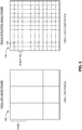
- FIG. 3 is a schematic illustration of a reconstructed image frame, referenced 164, formed from the image sub-frames of Figures 2A , 2B , 2C and 2D , compared with a regular image frame, referenced 162, of the imaging detector.
- Regular image frame 162 includes a total of 9 pixels (3x3), whereas reconstructed image frame 164 includes a total of 144 sub-pixels (12x12), providing a 16-fold increase in resolution (i.e., increasing the number of pixels by a factor of four along each of the horizontal and vertical axes).
- each individual pixel in reconstructed image frame 164 (corresponding to a pixel of image frame 162) is made up of 16 sub-pixels arranged in a 4x4 matrix.
- Each sub-pixel of reconstructed image frame 164 is formed from a combination of the respective sub-frames in which that sub-pixel was imaged.
- sub-pixel 168 of image frame 164 is formed based on sub-frames 1 and 2 ( Fig.2A ) and sub-frames 5 and 6 ( Fig.2B ), in which that particular sub-pixel portion of image scene 150 was acquired (in different configurations).
- Reconstructed image frame 164 represents a 16-fold increase in resolution with respect to image frame 162, which is an image frame that would result from regular imaging with detector array 110 (i.e., without application of the disclosed technique).
- the final image frame contains greater image detail (i.e., by a factor of sixteen) as compared to a standard image frame, as each pixel of the reconstructed image frame is made up of sixteen individual sub-pixels which provides four times the detail or information along each axis as would be contained in the corresponding pixel of the standard image frame.
- alternative resolution increase factors i.e., the amount by which the image resolution is increased
- the shifting increment may be set to be approximately one-ninth (1/9) of the detector pixel width, while each imaging sample would image a sub-region occupying an area of approximately one-ninth (1/9) of the image pixels (i.e., corresponding to a fill factor reduction factor of 1/9 or approximately 11%).
- a masking filter 130 having windows or non-masking regions 134 that are one-ninth (1/9) the size of the detector pixels may be used to provide imaging of the desired image pixel sub-region size, instead of the masking filter 130 shown in Figures 2A-2D which includes windows that are one-quarter (1/4) the detector pixel size.
- a total of 81 sub-frames would be acquired via microscanning (following a shifting increment of one-ninth (1/9) the detector pixel width between sub-frames), from which a final higher-resolution image frame can be reconstructed.
- the fill factor reduction of the detector pixels serves to reduce the overall detector sensitivity, as only a fraction of the entire radiation from the image scene reaches the detector array.
- the f-number also known as the "focal ratio", defined as the ratio between the entrance pupil diameter and the lens focal length
- the f-number decrease also provides an improved optical Modulation Transfer Function (MTF), generally representing the ability the detector to distinguish between detail in the acquired image, thereby allowing the detector to support the enhanced spatial resolution of the reconstructed image frame.
- MTF optical Modulation Transfer Function
- the disclosed technique enhances the performance of the IR imaging detector by essentially reducing the detector sensitivity (by reducing the fill factor) and compensating for this reduction by providing suitable detector optics that will provide an adequate level of overall sensitivity together with a substantially higher image spatial resolution
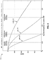
- FIG. 4 is a schematic illustration of a graph, generally referenced 170, showing Modulation Transfer Function (MTF) as a function of spatial frequency for different fill factor reduction amounts in accordance with the disclosed technique.
- Graph 170 depicts the detector MTF as a function of spatial frequency or "detector sampling frequency" (corresponding to a normalized representation of the spatial resolution).
- detector sampling frequency corresponding to a normalized representation of the spatial resolution.
- the potential fill factor reduction amount (and thus the potential resolution increase) that can actually be implemented for a given imaging detector is generally limited by opto-mechanical design constraints. Such limitations in the ability to design and manufacture the suitable high resolution optics may vary according to particular system design and requirements.
- fill factor reduction means 120 may be implemented using any suitable device, mechanism or technique operative for reducing the fill factor of the detector pixels by the desired amount.
- fill factor reduction means 120 may alternatively be implemented by only a masking filter, which is successively repositioned and/or reoriented to obtain different imaging samples, or by only an optical element, which adjusts the optical path of the radiation from the image scene 150 over successive increments for each imaging sample.
- fill factor reduction means 120 may be implemented by configuring detector array 110 such that the active (photosensitive) region of the pixels is less than the potentially maximum active region.
- the pixels may be electronically configured such that only a selected sub-pixel region is active during each imaging sample.
- the disclosed technique is applicable to all types of IR detectors, operative anywhere within the wavelength range of approximately 1-15 ⁇ m, encompassing LWIR, MWIR and SWIR wavelengths.
- the disclosed technique is particularly applicable to thermal imaging cameras, and particularly vacuum-sealed and cryogenically-cooled thermal imagers, where the term "cryogenically-cooled” as used herein encompasses different types of low-temperature detectors, including those operating at temperatures above what may be considered cryogenic temperatures under some definitions (for example, including temperatures between approximately -150°C (123K) and approximately -120°C (153K)).
Description
- The disclosed technique generally relates to infrared image detectors having a two-dimensional sensor array, and to image resolution enhancement.
- An infrared (IR) image detector forms an image by detecting radiation in the infrared portion of the electromagnetic spectrum from the imaged scene. A passive infrared detector operates by measuring the infrared radiation emitted by the sources, particularly thermal energy in the far infrared range, as opposed to active IR detectors which first illuminates the objects with IR radiation and then captures the reflections of the illuminations. The inherent spatial resolution of a detector with a two-dimensional matrix array is a function of the size and number of pixels within the array (the pixel density). For many types of image sensors, such as complementary metal-oxide-semiconductor (CMOS)-based or charge-coupled device (CCD)-based sensors, it is fairly straightforward to increase the resolution by adding more pixels within a fixed space and/or decreasing pixel size in the array. However, for IR sensors such an approach would be prohibitively difficult and expensive. Furthermore, IR detectors are prone to receiving scarce light (particularly with passive IR detectors), and usually requires manipulations or treatment in order to enhance the amount of radiation collected by the detector to enable effective imaging in the IR wavelength range.
-
U.K. Patent No. 2,270,230 to Hirose - European Patent No.
1,198,119 to Parsons , entitled "Improved resolution for an electric image sensor array", discloses introducing a partially occluding mask/light source between the sensor array and the image. Resolution improvement is obtained by displacement between the array and the mask/light source and calculating grey scale values for the improved resolution from the different changes in the charges of the individual array sensors. - PCT Application Publication No.
98/46007 to Bone -
U.S. Patent No. 6,005,682 to Wu et al , entitled "Resolution enhancement by multiple scanning with a low-resolution, two-dimensional sensor array", is directed to high-resolution imaging with low-resolution two-dimensional imagers whose sensors are only a fraction of a selected pixel area. Sensors are stepped across an image with an optical or mechanical stepper to acquire an image at each sensor position. Multiple images are obtained from individual sensors, which have a sensed area substantially less than the area of the pixels of the sensor array. The rescanning is accomplished by movable mirrors or lenses that are disposed between an illuminated specimen and a sensor area. -
U.S. Patent No. 5,712,685 to Dumas , entitled "Device to enhance imaging resolution", is directed to improving resolution of a Focal Plane Array (FPA) image sensor with microscanning methodology. A mask having a checkerboard pattern of opaque and transparent areas is located in front of and adjacent to the FPA onto which an image of a scene is optically focused. The mask and FPA are displaced with respect to each other in a number of micro-steps that extend in the same direction as the columns/rows of the FPA grid. The micro-steps are of equal lengths and are each a fraction of the length of a detector element. Opaque areas of the mask progressively cover equal areas of detector elements in discrete steps for each micro-step movement in one direction at the same time as transparent areas of the mask progressively uncover equal areas of other detector elements for each discrete step. Outputs from the detector elements provide signals for sample slices of the scene for each micro-step, and an image of the scene is reconstructed from the signals. - An article to Wang et al., entitled "The effect of fill factor of infrared FPA sensor on microscanning imagery quality", published in Proceedings of SPIE Vol. 5640, pp. 417-424, is directed to a study of optimum microscanning modes as a function of different fill factors in an infrared sensor. Microscanning is an important technique in the field of high-resolution IR imaging which can increase the system resolution and improve the performance of imaging systems. Under some assumptions, this article introduces the sampling-averaging MTF of a detector array at a spatial Nyquist frequency as a figure of merit to quantitatively evaluate the improvement of different microscanning modes to image quality for different fill factors (i.e., the following
fill factors -
U.S. Patent No. 5,371,369, issued to Kent and assigned to Litton Systems, Inc., entitled "Conformal Cold Baffle for Optical Imaging Systems" is directed to a cooled stray light baffle for use in an imaging system such as an infrared camera. The baffle includes a tapered shroud portion which is shaped to just enclose the envelope of light rays which pass through the baffle. Space between the envelope of light rays and the inner surface of the baffle is thus minimized resulting in a minimization of the overall surface area and mass of the baffle, which in turn results in a minimization of the refrigeration load of the system. The lower refrigeration load requires a smaller refrigerator which results in reduced system size, power consumption, vibration, cool-down time and cost of operation. The outer surface of the baffle is covered with a reflective material to reflect light photons. The inner surface is roughened and blackened to absorb stray light photons which enter the baffle. - An article to Fortin et al., entitled "Realization of a fast microscanning device for infrared focal plane arrays", published in Proceedings of SPIE Vol. 2743, pp.185-196, is directed to a microscanning technique for doubling the resolution of a given staring array imager. Microscanning consists in taking multiple images of the same scene while displacing each time the image over the detector plane by a distance equal to a fraction of the detector pitch. Microscanning is limited by the time required to shift the image from one point to the other and by the precision of the movements. This article describes a fast microscanning imaging device which includes three main sections: a microscanning head, a controller and a power amplifier. The microscanning head is made of a lens and a two-axis microtranslation table driven by two piezoelectric translators. The controller drives a high voltage power amplifier which in turn drives the translator. The controller allows four operation modes: fixed position, 2x2, 3x3 and 4x4 microscan and the system can work in an open as well as in a closed loop for precise displacements. The system can serve as an aid for the identification of detected objects.
- In accordance with one aspect of the disclosed technique, there is thus provided an apparatus for increasing the resolution of a cryogenically cooled and vacuum-sealed infrared imaging detector according to
claim 1. The apparatus includes a two-dimensional detector array of photosensitive pixels arranged in a matrix, a masking filter, an optical element, shifting means, and a processor. The detector array is operative within the wavelength range of 1-15 µm and is successively exposed to an image scene, to acquire multiple imaging samples of the scene. The masking filter is disposed between the detector array and the image scene and is maintained at a fixed position with respect to the detector array. The masking filter masks part of the active region of the pixels within the wavelength range of 1-15 µm by a fill factor reduction amount, for each of the imaging samples, such that only a portion of each pixel area of the image scene is imaged onto the corresponding masked pixel of the detector array. The optics are disposed between the masking filter and the image scene, and direct the incident radiation onto the detector array through the masking filter. The shifting means successively shifts the optical path of the image scene relative to the masking filter and the detector array between each of the imaging samples, by a shifting increment corresponding to the fill factor reduction amount, to provide imaging of different sub-pixel regions in each of the imaging samples. The processor reconstructs an image frame from the acquired imaging samples, the reconstructed image frame having a resolution greater than the intrinsic resolution of the detector, by a factor defined by the fill factor reduction amount. The masking filter may be a coating disposed on the detector array. The masking filter may include configuring the detector array such that the photosensitive region of the pixels of the array is smaller than the potentially maximum photosensitive region of the pixels. The shifting means may shift the optical path of the image scene relative to the masking filter by repositioning the optics with respect to the masking filter and the detector array. The shifting means may alternatively shift the optical path of the image scene relative to the masking filter and the detector array by jointly repositioning the masking filter and the detector array with respect to the optics. The f-number of the detector optics may be selected in accordance with to the fill factor reduction amount to provide a selected sensitivity of the detector. The selected sensitivity of the detector may correspond to the sensitivity of a non-fill factor reduced detector. The detector may be a thermal imaging detector. - In accordance with another aspect of the disclosed technique, there is thus provided a method for increasing the resolution of a cryogenically cooled and vacuum-sealed infrared imaging detector according to
claim 9, the detector includes a two-dimensional detector array of photosensitive pixels arranged in a matrix, the detector array operative within the wavelength range of 1-15 µm. The method includes the procedures of successively exposing the detector array to an image scene to acquire multiple imaging samples of the scene, and masking part of the active region of the pixels within the wavelength range of 1-15 µm by a fill factor reduction amount, for each of the imaging samples, via a masking filter disposed within the cryogenic storage dewar and maintained at a fixed position with respect to the detector array, such that only a portion of each pixel area of the image scene is imaged onto the corresponding masked pixel of the detector array. The method further includes the procedure of successively shifting the optical path of the image scene relative to the masking filter and the detector array between each of the imaging samples, , by a shifting increment corresponding to the fill factor reduction amount, to provide imaging of different sub-pixel regions in each of the imaging samples. The method further includes the procedure of reconstructing an image frame from the acquired imaging samples, the reconstructed image frame having a resolution greater than the intrinsic resolution of the detector, by a factor defined by the fill factor reduction amount. The method may further include the procedure of selecting the f-number of the detector optics in accordance with the fill factor reduction amount to provide a selected sensitivity of the detector. The selected sensitivity of the detector may correspond to the sensitivity of a non-fill factor reduced detector. - The disclosed technique will be understood and appreciated more fully from the following detailed description taken in conjunction with the drawings in which:
-
Figure 1 is a perspective view schematic illustration of an apparatus for increasing the resolution of an infrared imaging detector, constructed and operative in accordance with an embodiment of the disclosed technique; -
Figure 2A is a perspective view schematic illustration of an initial set of image sub-frames acquired over successive imaging samples with the apparatus ofFigure 1 ; -
Figure 2B is a perspective view schematic illustration of a subsequent set of image sub-frames acquired over successive imaging samples with the apparatus ofFigure 1 ; -
Figure 2C is a perspective view schematic illustration of another subsequent set of image sub-frames acquired over successive imaging samples with the apparatus ofFigure 1 ; -
Figure 2D is a perspective view schematic illustration of a final set of image sub-frames acquired over successive imaging samples with the apparatus ofFigure 1 ; -
Figure 3 is a schematic illustration of a reconstructed image frame, formed from the image sub-frames ofFigures 2A ,2B ,2C and2D , compared with a regular image frame of the imaging detector; and -
Figure 4 is a schematic illustration of a graph showing Modulation Transfer Function (MTF) as a function of spatial frequency for different fill factor reduction amounts in accordance with the disclosed technique. - The disclosed technique overcomes the disadvantages of the prior art by providing a method and apparatus for increasing the intrinsic resolution of an infrared (IR) imaging detector without increasing the total size or the pixel density of the detector array. Instead, the effective spatial resolution of the IR detector is enlarged by reducing the active region within the individual pixels of the detector array (i.e., reducing the "fill factor"). Multiple imaging samples of the same image scene are acquired, in which only a portion of each pixel of the image scene is imaged onto the corresponding pixel of the detector array. The image scene is successively shifted relative to the detector array to provide imaging of different configurations of sub-pixel regions in each of the imaging samples. A higher resolution image frame is then reconstructed from the individual imaging samples.
- Reference is now made to
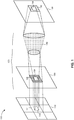
Figure 1 , which is a perspective view schematic illustration of an apparatus, generally referenced 100, for increasing the resolution of an infrared imaging detector, constructed and operative in accordance with an embodiment of the disclosed technique.Apparatus 100 includes anIR detector array 110, and a fill factor reduction means 120 made up of a maskingfilter 130 and anoptical element 140. Maskingfilter 130 andoptical element 140 are disposed in betweendetector array 110 and thescene 150 to be imaged by the detector.Detector array 110 is made up of a lattice or matrix pattern of photosensitive pixels arranged in rows and columns (e.g., a 320x240 array, which includes 320 pixels along the array width and 240 pixels along the array height). The pixels inarray 110 may be any suitable size or area, where the individual pixel size is generally substantially consistent across all pixels of the array. Fill factor reduction means 120 is operative to selectively reduce the active (i.e., photosensitive) region of the pixels ofdetector array 110, by masking or blocking a portion of the photosensitive region of the pixels from receiving radiation from the image scene, such that only a portion of the image scene pixel is imaged onto the corresponding detector array pixel. The active region and masked region of the pixels are then progressively shifted during subsequent imaging samples of the scene. In particular,optical element 140 projects animage region 152 ofimage scene 150 onto maskingfilter 130, which in turn blocks out a portion ofimage region 152 from reaching thecorresponding pixel 111 of detector array while allowing only the remainingportion 154 ofimage region 152 to reachpixel 111. Consequently,pixel 111 includes an imagedregion 114 that is less than the total area (i.e., potential photosensitive area) ofarray pixel 111. Maskingfilter 130 includes amasking region 132 and anon-masking region 134, such that radiation incident onto masking region 132 (via optical element 140) is prevented from passing through (toward detector array 110), while radiation incident ontonon-masking region 134 is passed through. For example, maskingregion 132 may be embodied by a substantially opaque or non-transmissive portion of filter or a non-transmissive coating disposed at the required portion, whereasnon-masking region 134 may be embodied by a substantially transmissive portion offilter 130, such as a window or opening thereat. - It is noted that any of the components of fill factor reduction means 120 may be fully or partially integrated with the IR imaging detector in accordance with the disclosed technique, or may be separate therefrom. For example, masking
filter 130 may be situated within the housing enclosing the IR detector, whileoptical element 140 may be situated outside of the housing, providedoptical element 140 and masking filter function to implement the aforementioned masking operation of theimage scene 150 onto thedetector array 110. - Reference is now made to
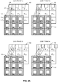
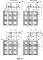
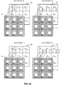
Figures 2A ,2B ,2C and2D .Figure 2A is a perspective view schematic illustration of an initial set of image sub-frames acquired over successive imaging samples with the apparatus ofFigure 1 .Figure 2B is a perspective view schematic illustration of a subsequent set of image sub-frames acquired over successive imaging samples with the apparatus ofFigure 1 .Figure 2C is a perspective view schematic illustration of another subsequent set of image sub-frames acquired over successive imaging samples with the apparatus ofFigure 1 .Figure 2D is a perspective view schematic illustration of a final set of image sub-frames acquired over successive imaging samples with the apparatus ofFigure 1 .Detector array 110 is depicted with nine (9) pixels arranged in a three-by-three (3x3) matrix. Maskingfilter 130 is disposed directly onarray 110, and includes nine windows (i.e., non-masking regions 134) situated on a sub-region of each of the detector pixels (DPx,y) ofdetector array 110, while the remaining area of maskingfilter 130 is made up of maskingregions 132. Theimage scene 150 is similarly divided into nine image pixels (IPx,y) arranged in a three-by-three (3x3) matrix (i.e., each image pixel representing the region ofimage scene 150 that would ordinarily be projected onto a corresponding detector pixel during regular image acquisition). - A first set of sub-frames of
image scene 150 is acquired inFig. 2A . The light (IR radiation) emitted fromimage scene 150 is directed towarddetector array 110 through maskingfilter 130 via optical element 140 (not shown), such that only the radiation passing through thewindows 134 of maskingfilter 130 reachesdetector array 110. In particular, each detector pixel ofdetector array 110 captures a portion of a corresponding image pixel ofimage scene 150. For example, referring to the first imaging sample ("sub-frame 1") inFig.2A , radiation corresponding to an upper-left corner image pixel (IP1,1) is directed toward a detector pixel (DP1,1) situated at the upper-left corner ofdetector array 110. A portion of the radiation (154) passes through the masking filter window and is incident onto the asub-region 114 of detector pixel DP1,1. The rest of the radiation (152) from image pixel IP1,1 is blocked by the maskingregion 132, such that it does not reach detector pixel DP1,1. Consequently, detector pixel DP1,1 includes an imagedregion 114 and anon-imaged region 112. Similarly, the next image pixel (IP1,2) in the top row ofimage scene 150 reaches detector pixel DP1,2 after passing through the masking filter window, such that only a portion of image pixel IP1,2 is incident onto a sub-region of detector pixel DP1,2. Fill factor reduction means 120 is shown implementing an exemplary fill factor reduction of 25% (i.e., "25%FF"), denoting that each imagedregion 114 occupies approximately one-quarter of the area of the respective pixel, while eachnon-imaged region 112 occupies an area of approximately three-quarters of the respective pixel. The remaining pixels (DPx,y) ofdetector array 110 are imaged in an analogous manner during the first imaging sample (sub-frame), resulting in each detector pixel acquiring an imagedregion 114 at its upper-left quadrant, while the remainder of the detector pixel is non-imaged. - Following acquisition of the first imaging sample, the portion of each image pixel imaged onto
detector array 110 is shifted for the subsequent imaging samples. The shifting increment between each imaging sample is selected in accordance with the fill factor reduction amount, and is generally equal to a fraction of the pixel width (defined as the distance between the midpoint of adjacent pixels of the detector array). In this example, the fill factor reduction amount is 25% (25%FF), and so the shifting increment is also selected to be 25%, or approximately one quarter of the pixel width of the detector pixels. The shifting may be implemented by adjusting the line-of-sight of fill factor reduction means 120 relative to detector array 110 (e.g., by suitable adjustment of maskingfilter 130 and/or of optical element 140). Referring to the second imaging sample ("sub-frame 2") inFig.2A , each detector pixel DPx,y receives incident radiation from another portion of image pixel IPx,y, such that the imagedregion 114 corresponds to an upper-middle quadrant of the corresponding image pixel IPx,y (e.g., the imaged quadrant of "sub-frame 1" being shifted to the right by a quarter of the pixel width, such that the second image quadrant partially overlaps the first image quadrant). Referring to the third imaging sample ("sub-frame 3"), the line-of-sight is shifted again such that the imagedregion 114 of each detector pixel DPx,y corresponds to an upper-right quadrant of the corresponding image pixel IPx,y (e.g., the imaged quadrant of "sub-frame 2" being shifted to the right by a quarter of the pixel width). - Additional imaging samples are acquired in an analogous manner, covering remaining overlapping portions (e.g., quadrants) of each image pixel, by successively adjusting the line-of-sight systematically over the same shifting increment (e.g., a quarter pixel width) along both the vertical axis and the horizontal axis of the
image scene 150, applying a technique called "microscanning", known in the art. For example, referring to the fifth imaging sample ("sub-frame 5") inFig.2B , the line-of-sight is shifted downwards by the shifting increment with respect to the first imaging sample, such that the imagedregion 114 of each detector pixel DPx,y corresponds to an middle-left quadrant of the corresponding image pixel IPx,y (e.g., the imaged quadrant of "sub-frame 1" being shifted downwards by a quarter of the pixel width). The remaining imaging samples ("sub frame 6" through "sub-frame 16") result in additional image pixel portions being acquired (i.e., imaging a respective portion that was not acquired in a previous sub-frame). - The line-of-sight alignment of fill factor reduction means 120 relative to
detector array 110 may be successively shifted using any suitable mechanism or technique, in order to obtain the desired imaged sub-region on the detector pixels for each imaging sample. For example, maskingfilter 130 anddetector array 110 remain in a fixed position, and thus the positions of maskingregions 132 andnon-masking regions 134 remain stationary, whileoptical element 140 is successively repositioned for each imaging sample to shift the directional angle at whichoptical element 140 directs the radiation fromimage scene 150. Alternatively, maskingfilter 130 anddetector array 110 are jointly repositioned relative to optical element 140 (i.e., where maskingfilter 130 remains fixed with respect to detector array 110), for adjusting the optical path ofimage scene 150 for each imaging sample. It is noted that the actual size of the imaged regions on the detector pixels may be varied, such as by adjusting the characteristics of masking filter 130 (e.g., size, amount, and/or relative positions of non-masking regions 134) and/or adjusting the optical characteristics ofoptical element 140. In some detectors, such as vacuum-sealed detector and/or cryogenically-cooled detectors, it is very difficult to reposition a masking filter relative to the detector array, since the two components should be arranged as close as possible to one another. Consequently, a mechanism for repositioning a movable masking filter would need to be situated within the cryogenic storage dewar (vacuum flask) along with the masking filter and detector array. This requires such a mechanism to be exceptionally miniature and fast moving, while being capable of operating in cryogenic temperatures. Furthermore, the cryogenic storage dewar would require significant enlargement, as well as an enhanced cooling mechanism to support the additional heating load. Thus, even if the implementation of a movable masking filter is feasible, the aforementioned issues would yield a detector with minimal practical applications due to the resultant high cost, higher power consumption, greater volume, and lower reliability. Therefore, according to an embodiment of the disclosed technique, a stationary masking filter is maintained at a fixed position and orientation relative to the detector array, while the optical path of the image scene is successively adjusted relative to the stationary masking filter between imaging samples. - The different sub-regions of the image pixels IPx,y of
image scene 150 may be imaged in any order or permutation. For example, a bottom row of image pixel portions may be imaged first (i.e., the four sub-frames depicted inFig.2D ), followed by a higher row, and so forth; or alternatively, a first column of image pixel portions may be imaged in a first group of sub-frames, followed by an adjacent column, and so forth. Furthermore, the imaged sub-regions may be nonconsecutive within a given sub-frames (e.g., an upper-left quadrant and lower-right quadrant of the image pixel may be simultaneously acquired in one sub-frame, while an upper-right quadrant and lower-left quadrant of the image pixel are simultaneously acquired in a subsequent sub-frame). - After all the sub-frames are acquired over successive imaging samples, where each individual sub-frame corresponds to a different imaged sub-region of each image pixel of
image scene 150, a final image frame is constructed from all of the acquired sub-frames. Namely, all of the imaged sub-regions for each image pixel are processed and combined, in accordance with a suitable image processing scheme. Reference is now made toFigure 3 , which is a schematic illustration of a reconstructed image frame, referenced 164, formed from the image sub-frames ofFigures 2A ,2B ,2C and2D , compared with a regular image frame, referenced 162, of the imaging detector.Regular image frame 162 includes a total of 9 pixels (3x3), whereasreconstructed image frame 164 includes a total of 144 sub-pixels (12x12), providing a 16-fold increase in resolution (i.e., increasing the number of pixels by a factor of four along each of the horizontal and vertical axes). In particular, each individual pixel in reconstructed image frame 164 (corresponding to a pixel of image frame 162) is made up of 16 sub-pixels arranged in a 4x4 matrix. Each sub-pixel ofreconstructed image frame 164 is formed from a combination of the respective sub-frames in which that sub-pixel was imaged. For example,sub-pixel 168 ofimage frame 164 is formed based onsub-frames 1 and 2 (Fig.2A ) andsub-frames 5 and 6 (Fig.2B ), in which that particular sub-pixel portion ofimage scene 150 was acquired (in different configurations). -
Reconstructed image frame 164 represents a 16-fold increase in resolution with respect toimage frame 162, which is an image frame that would result from regular imaging with detector array 110 (i.e., without application of the disclosed technique). The intrinsic resolution ofdetector array 110 is represented by a 3x3 pixel density (i.e., 3 rows by 3 columns of pixels = 9 total pixels), as depicted inimage frame 162, whereasreconstructed image frame 164 includes 12x12 sub-pixels within the same fixed area ofarray 110. As a result, the final image frame contains greater image detail (i.e., by a factor of sixteen) as compared to a standard image frame, as each pixel of the reconstructed image frame is made up of sixteen individual sub-pixels which provides four times the detail or information along each axis as would be contained in the corresponding pixel of the standard image frame. - It is appreciated that alternative resolution increase factors (i.e., the amount by which the image resolution is increased) may be obtained by varying the shifting increment between sub-frames, as well as the fill factor reduction amount (i.e., the amount by which the active region of the detector pixels is reduced). For example, to increase the image resolution by a factor of 9 (along each of the horizontal and vertical axes), then the shifting increment would be set to be approximately one-ninth (1/9) of the detector pixel width, while each imaging sample would image a sub-region occupying an area of approximately one-ninth (1/9) of the image pixels (i.e., corresponding to a fill factor reduction factor of 1/9 or approximately 11%). For example, a masking
filter 130 having windows ornon-masking regions 134 that are one-ninth (1/9) the size of the detector pixels, may be used to provide imaging of the desired image pixel sub-region size, instead of the maskingfilter 130 shown inFigures 2A-2D which includes windows that are one-quarter (1/4) the detector pixel size. A total of 81 sub-frames would be acquired via microscanning (following a shifting increment of one-ninth (1/9) the detector pixel width between sub-frames), from which a final higher-resolution image frame can be reconstructed. - It is noted that the fill factor reduction of the detector pixels serves to reduce the overall detector sensitivity, as only a fraction of the entire radiation from the image scene reaches the detector array. To compensate for this effect, the f-number (also known as the "focal ratio", defined as the ratio between the entrance pupil diameter and the lens focal length) of the detector optics is decreased by a factor corresponding to the fill factor reduction amount (or to the shifting increment between imaging samples). Consequently, more radiation is received from the image scene, which offsets the reduction in received radiation resulting from the fill factor reduction. The f-number decrease also provides an improved optical Modulation Transfer Function (MTF), generally representing the ability the detector to distinguish between detail in the acquired image, thereby allowing the detector to support the enhanced spatial resolution of the reconstructed image frame. Thus, the disclosed technique enhances the performance of the IR imaging detector by essentially reducing the detector sensitivity (by reducing the fill factor) and compensating for this reduction by providing suitable detector optics that will provide an adequate level of overall sensitivity together with a substantially higher image spatial resolution
- Reference is now made to
Figure 4 , which is a schematic illustration of a graph, generally referenced 170, showing Modulation Transfer Function (MTF) as a function of spatial frequency for different fill factor reduction amounts in accordance with the disclosed technique.Graph 170 depicts the detector MTF as a function of spatial frequency or "detector sampling frequency" (corresponding to a normalized representation of the spatial resolution). When implementing "regular microscanning" to increase the resolution of the detector (i.e., without reducing the fill factor of the detector pixels), then the resolution increase (additional information that can be derived from the image) is limited by the detector Nyquist frequency (where the Nyquist frequency equals half the pixel spatial sampling frequency). For example, when imaging without any fill factor reduction (i.e., "100%FF"), shifting between each microscan at increments of less than half the detector pixel pitch would not increase the overall image resolution beyond a factor of x2 (since the MTF reaches zero beyond the "2X Microscan" frequency point on the graph, and is thus essentially unusable for imaging purposes). In contrast, when implementing microscanning in conjunction with fill factor reduction, then the spatial resolution of the detector image can be increased by a larger factor (i.e., not limited by the detector Nyquist frequency) while still deriving additional information from the image. For example, if the fill factor is decreased to 25% of the total active pixel area ("25%FF"), it is possible to microscan at shifting increments of up to 1/4 of the detector pixel pitch (thereby increasing image resolution by x4 along each axis =x16 total), while still being able to distinguish between the additional information (since the MTF is still above zero). By reducing the fill factor even further, it is possible to microscan at higher frequencies/smaller shifting increments to provide an even larger resolution increase. It is noted that the potential fill factor reduction amount (and thus the potential resolution increase) that can actually be implemented for a given imaging detector is generally limited by opto-mechanical design constraints. Such limitations in the ability to design and manufacture the suitable high resolution optics may vary according to particular system design and requirements. - Referring back to
Figure 1 , fill factor reduction means 120 may be implemented using any suitable device, mechanism or technique operative for reducing the fill factor of the detector pixels by the desired amount. For example, fill factor reduction means 120 may alternatively be implemented by only a masking filter, which is successively repositioned and/or reoriented to obtain different imaging samples, or by only an optical element, which adjusts the optical path of the radiation from theimage scene 150 over successive increments for each imaging sample. Further alternatively, fill factor reduction means 120 may be implemented by configuringdetector array 110 such that the active (photosensitive) region of the pixels is less than the potentially maximum active region. For example, the pixels may be electronically configured such that only a selected sub-pixel region is active during each imaging sample. - The disclosed technique is applicable to all types of IR detectors, operative anywhere within the wavelength range of approximately 1-15 µm, encompassing LWIR, MWIR and SWIR wavelengths. The disclosed technique is particularly applicable to thermal imaging cameras, and particularly vacuum-sealed and cryogenically-cooled thermal imagers, where the term "cryogenically-cooled" as used herein encompasses different types of low-temperature detectors, including those operating at temperatures above what may be considered cryogenic temperatures under some definitions (for example, including temperatures between approximately -150°C (123K) and approximately -120°C (153K)).
- In accordance with the disclosed technique, there is provided a method for increasing the resolution of an IR imaging detector comprising a two-dimensional detector array of photosensitive pixels arranged in a matrix. The method includes the procedure of successively exposing the detector array to an image scene, to acquire multiple imaging samples of the image scene, where for each imaging sample, the region of the pixels collecting incident radiation from the image scene is reduced such that only a portion of the pixel area of the imaged scene is imaged onto the corresponding pixel of the detector array. The method further includes the procedure of successively shifting the image scene relative to the detector array by a shifting increment equal to a fraction of the pixel width of the array pixels, to provide imaging of successive sub-pixel region in each of the imaging samples. The method further includes the procedure of reconstructing an image frame having a resolution greater, by a factor defined by the shifting increment, than the intrinsic resolution of the detector, from the acquired imaging samples.
- It will be appreciated by persons skilled in the art that the disclosed technique is not limited to what has been particularly shown and described hereinabove.
Claims (11)
- An apparatus (100) for increasing the resolution of an infrared imaging detector, comprising:a two-dimensional infrared detector array of photosensitive pixels (111) arranged in a matrix (110), said detector array having a fill factor value, said detector array successively exposed to an image scene (150), to acquire multiple infrared imaging samples of said scene;characterized in that:said infrared imaging detector is cryogenically cooled and vacuum-sealed;said detector array is operative within a wavelength range of 1-15 µm;said apparatus further comprising:a masking filter (130) having a single pattern and disposed between said detector array and said image scene and maintained at a fixed position with respect to said detector array, said masking filter configured to mask (112) part of an active region of said pixels within said wavelength range thereby reducing said fill factor value by a fill factor reduction amount, for each of said imaging samples, such that only a sub-region (154) of a pixel region of said image scene is imaged onto a corresponding masked pixel of said detector array;optics (140), disposed between said masking filter and said image scene, said optics configured to direct said image scene onto said detector array through said masking filter;shifting means, for successively shifting the optical path of said image scene relative to said detector array between each of said imaging samples, by a shifting increment corresponding to said fill factor reduction amount and smaller than an unmasked active region (114) of a masked photosensitive pixel, wherein each masked photosensitive pixel of said detector array receives partially overlapping sub-regions in said imaging samples; anda processor, configured to reconstruct an image frame from said acquired imaging samples, said reconstructed image frame having a resolution greater than an intrinsic resolution of said detector array by a factor defined by said fill factor reduction amount.
- The apparatus of claim 1, wherein said masking filter comprises a coating disposed on said detector array.
- The apparatus of claim 1, wherein said masking filter comprises configuring said detector array such that a photosensitive region of said pixels of said array is smaller than a potentially maximum photosensitive region of said pixels.
- The apparatus of claim 1, wherein said shifting means is configured to shift an optical path of said image scene relative to said masking filter and said detector array by repositioning said optics with respect to said masking filter and said detector array.
- The apparatus of claim 1, wherein said shifting means is configured to shift an optical path of said image scene relative to said masking filter and said detector array by jointly repositioning said masking filter and said detector array with respect to said optics.
- The apparatus of claim 1, wherein an f-number of said optics is selected in accordance with said fill factor reduction amount to provide a selected sensitivity of said detector.
- The apparatus of claim 6, wherein said selected sensitivity of said detector corresponds to an adequate level of overall sensitivity.
- The apparatus of claim 1, wherein said detector is a thermal imaging detector.
- A method for increasing the resolution of an infrared imaging detector comprising a two-dimensional infrared detector array of photosensitive pixels arranged in a matrix, said detector array having a fill factor value, the method comprising the procedures of:successively exposing said detector array to an image scene, to acquire multiple infrared imaging samples of said scene;characterized in that:said infrared imaging detector is cryogenically cooled and vacuum-sealed;said detector array is operative within a wavelength range of 1-15 µm;masking part of an active region of said pixels within said wavelength range thereby reducing said fill factor value by a fill factor reduction amount for each of said imaging samples, via a masking filter having a single pattern, maintained at a fixed position with respect to said detector array, such that only a sub-region of a pixel region of said image scene is imaged onto a corresponding masked pixel of said detector array;successively shifting the optical path of said image scene relative to said detector array between each of said imaging samples, by a shifting increment corresponding to said fill factor reduction amount and smaller than an unmasked active region of a masked photosensitive pixel, wherein each masked photosensitive pixel of said detector array receives partially overlapping sub-regions in said imaging samples; andreconstructing an image frame from said acquired imaging samples, said reconstructed image frame having a resolution greater than an intrinsic resolution of said detector array by a factor defined by said fill factor reduction amount.
- The method of claim 9, further comprising the procedure of selecting an f-number of a detector optics in accordance with said fill factor reduction amount to provide a selected sensitivity of said detector.
- The method of claim 10, wherein said selected sensitivity of said detector corresponds to an adequate level of overall sensitivity.
Priority Applications (1)
| Application Number | Priority Date | Filing Date | Title |
|---|---|---|---|
| PL13729475T PL2837173T3 (en) | 2012-05-13 | 2013-05-05 | Infrared detector with increased image resolution |
Applications Claiming Priority (2)
| Application Number | Priority Date | Filing Date | Title |
|---|---|---|---|
| IL219773A IL219773A (en) | 2012-05-13 | 2012-05-13 | Apparatus and method for increasing the resolution of a cryogenically cooled and vacuum-sealed infrared imaging detector |
| PCT/IL2013/050380 WO2013171738A1 (en) | 2012-05-13 | 2013-05-05 | Infrared detector with increased image resolution |
Publications (2)
| Publication Number | Publication Date |
|---|---|
| EP2837173A1 EP2837173A1 (en) | 2015-02-18 |
| EP2837173B1 true EP2837173B1 (en) | 2017-03-22 |
Family
ID=48628762
Family Applications (1)
| Application Number | Title | Priority Date | Filing Date |
|---|---|---|---|
| EP13729475.7A Active EP2837173B1 (en) | 2012-05-13 | 2013-05-05 | Infrared detector with increased image resolution |
Country Status (11)
| Country | Link |
|---|---|
| US (2) | US9894292B2 (en) |
| EP (1) | EP2837173B1 (en) |
| JP (1) | JP6083833B2 (en) |
| KR (1) | KR102043325B1 (en) |
| BR (1) | BR112014028169B1 (en) |
| CA (1) | CA2873196C (en) |
| ES (1) | ES2626070T3 (en) |
| IL (1) | IL219773A (en) |
| PL (1) | PL2837173T3 (en) |
| SG (1) | SG11201407311RA (en) |
| WO (1) | WO2013171738A1 (en) |
Families Citing this family (8)
| Publication number | Priority date | Publication date | Assignee | Title |
|---|---|---|---|---|
| IL219773A (en) * | 2012-05-13 | 2015-09-24 | Elbit Sys Electro Optics Elop | Apparatus and method for increasing the resolution of a cryogenically cooled and vacuum-sealed infrared imaging detector |
| JP6361965B2 (en) * | 2013-10-24 | 2018-07-25 | パナソニックIpマネジメント株式会社 | Imaging system, imaging apparatus, encoding apparatus, and imaging method |
| KR102357965B1 (en) * | 2015-01-12 | 2022-02-03 | 삼성전자주식회사 | Method of recognizing object and apparatus thereof |
| CN105547490B (en) * | 2015-12-08 | 2019-01-25 | 中国科学院上海技术物理研究所 | A kind of real-time blind pixel detection method of number TDI infrared detector |
| EP4111179A4 (en) * | 2020-02-27 | 2023-11-15 | Shenzhen Xpectvision Technology Co., Ltd. | Imaging system |
| IL274418B (en) * | 2020-05-03 | 2021-12-01 | Elbit Systems Electro Optics Elop Ltd | Systems and methjods for enhanced motion detection, object tracking, situational awareness and super-resolution video using microscanned images |
| US11651474B2 (en) | 2020-11-04 | 2023-05-16 | Bae Systems Information And Electronic Systems Integration Inc. | Real-time super resolution at long standoff ranges |
| CN115546486A (en) * | 2022-10-17 | 2022-12-30 | 深圳市元视芯智能科技有限公司 | Bionic vision sensor, imaging method and unmanned aerial vehicle image transmission system |
Family Cites Families (17)
| Publication number | Priority date | Publication date | Assignee | Title |
|---|---|---|---|---|
| JPS61264874A (en) * | 1985-05-20 | 1986-11-22 | Fujitsu General Ltd | Solid-state image pickup device |
| JPH0682305A (en) | 1992-08-31 | 1994-03-22 | Shimadzu Corp | Two-dimensional detector |
| US5371369A (en) | 1993-10-13 | 1994-12-06 | Litton Systems, Inc. | Conformal cold baffle for optical imaging systems |
| CA2135676A1 (en) | 1994-11-14 | 1996-05-15 | Jean Dumas | Device to enhance imaging resolution |
| US6005682A (en) | 1995-06-07 | 1999-12-21 | Xerox Corporation | Resolution enhancement by multiple scanning with a low-resolution, two-dimensional sensor array |
| AUPO615297A0 (en) | 1997-04-10 | 1997-05-08 | Commonwealth Scientific And Industrial Research Organisation | Imaging system and method |
| JPH11331857A (en) * | 1998-05-13 | 1999-11-30 | Mitsubishi Electric Corp | Image pickup device |
| EP1198119A3 (en) | 2000-10-11 | 2004-05-26 | Charles E. Parsons | Improved resolution for an electric image sensor array |
| US7283231B2 (en) * | 2004-07-20 | 2007-10-16 | Duke University | Compressive sampling and signal inference |
| JP5000395B2 (en) * | 2007-06-26 | 2012-08-15 | オリンパス株式会社 | Imaging display method and imaging display device |
| GB2462137B (en) * | 2008-06-25 | 2013-01-23 | Thales Holdings Uk Plc | Imaging apparatus and method |
| JP4494505B1 (en) * | 2009-02-13 | 2010-06-30 | シャープ株式会社 | Image processing apparatus, imaging apparatus, image processing method, image processing program, and recording medium |
| US9291506B2 (en) * | 2010-01-27 | 2016-03-22 | Ci Systems Ltd. | Room-temperature filtering for passive infrared imaging |
| JP5341010B2 (en) * | 2010-04-15 | 2013-11-13 | オリンパス株式会社 | Image processing apparatus, imaging apparatus, program, and image processing method |
| US8866951B2 (en) * | 2011-08-24 | 2014-10-21 | Aptina Imaging Corporation | Super-resolution imaging systems |
| US10110834B2 (en) * | 2011-11-07 | 2018-10-23 | Raytheon Company | Hadamard enhanced sensors |
| IL219773A (en) * | 2012-05-13 | 2015-09-24 | Elbit Sys Electro Optics Elop | Apparatus and method for increasing the resolution of a cryogenically cooled and vacuum-sealed infrared imaging detector |
-
2012
- 2012-05-13 IL IL219773A patent/IL219773A/en active IP Right Grant
-
2013
- 2013-05-05 CA CA2873196A patent/CA2873196C/en active Active
- 2013-05-05 PL PL13729475T patent/PL2837173T3/en unknown
- 2013-05-05 BR BR112014028169-6A patent/BR112014028169B1/en active IP Right Grant
- 2013-05-05 SG SG11201407311RA patent/SG11201407311RA/en unknown
- 2013-05-05 EP EP13729475.7A patent/EP2837173B1/en active Active
- 2013-05-05 WO PCT/IL2013/050380 patent/WO2013171738A1/en active Application Filing
- 2013-05-05 KR KR1020147035168A patent/KR102043325B1/en active IP Right Grant
- 2013-05-05 JP JP2015512193A patent/JP6083833B2/en active Active
- 2013-05-05 ES ES13729475.7T patent/ES2626070T3/en active Active
- 2013-05-05 US US13/978,054 patent/US9894292B2/en not_active Expired - Fee Related
-
2018
- 2018-01-10 US US15/866,799 patent/US10547799B2/en active Active
Also Published As
| Publication number | Publication date |
|---|---|
| JP6083833B2 (en) | 2017-02-22 |
| ES2626070T3 (en) | 2017-07-21 |
| JP2015519567A (en) | 2015-07-09 |
| CA2873196C (en) | 2019-02-19 |
| BR112014028169A2 (en) | 2020-05-05 |
| BR112014028169B1 (en) | 2023-04-04 |
| US10547799B2 (en) | 2020-01-28 |
| AU2013261047A1 (en) | 2014-12-04 |
| US20180160056A1 (en) | 2018-06-07 |
| EP2837173A1 (en) | 2015-02-18 |
| US20140139684A1 (en) | 2014-05-22 |
| US9894292B2 (en) | 2018-02-13 |
| KR20150013795A (en) | 2015-02-05 |
| IL219773A (en) | 2015-09-24 |
| PL2837173T3 (en) | 2017-08-31 |
| KR102043325B1 (en) | 2019-12-02 |
| CA2873196A1 (en) | 2013-11-21 |
| SG11201407311RA (en) | 2014-12-30 |
| WO2013171738A1 (en) | 2013-11-21 |
Similar Documents
| Publication | Publication Date | Title |
|---|---|---|
| US10547799B2 (en) | Infrared detector with increased image resolution | |
| US11681061B2 (en) | Apparatus and method for capturing still images and video using diffraction coded imaging techniques | |
| EP1856710B1 (en) | Apparatus and method for capturing still images and video using coded lens imaging techniques | |
| US7888626B2 (en) | Coded aperture imaging system having adjustable imaging performance with a reconfigurable coded aperture mask | |
| WO2010048618A1 (en) | Systems and methods for high resolution imaging | |
| US20120081511A1 (en) | Interlaced focal plane array for wide-area surveillance | |
| Ben-Ezra | A digital gigapixel large-format tile-scan camera | |
| JP3335369B2 (en) | Imager | |
| US6642497B1 (en) | System for improving image resolution via sensor rotation | |
| Blommel et al. | Effects of microscan operation on staring infrared sensor imagery | |
| AU2013261047B2 (en) | Infrared detector with increased image resolution | |
| GB2428926A (en) | Imaging device including a pixel sensor array and scene radiation focusing and dislplacement means | |
| Falcone et al. | Hybrid CMOS x-ray detectors: the next generation for focused x-ray telescopes | |
| Göttfert et al. | Optimizing microscan for radiometry with cooled IR cameras | |
| Sims et al. | A CMOS visible image sensor with non-destructive readout capability | |
| US11861849B2 (en) | Systems and methods for enhanced motion detection, object tracking, situational awareness and super resolution video using microscanned images | |
| Greiner et al. | Resolution performance improvements in staring imaging systems using micro-scanning and a reticulated, selectable fill factor InSb FPA | |
| Chambers et al. | Reimaging system for evaluating high-resolution charge-coupled-device arrays | |
| Patel et al. | SPITFIRE multi-band short-wave and mid-wave polarimetric camera | |
| Portnoy et al. | Resolution and interpolation of multichannel long wave infrared camera data | |
| McGinn et al. | Implementation of a second-generation long-linear imager for the high-performance application | |
| Gilmore | The Large Synoptic Survey Telescope |
Legal Events
| Date | Code | Title | Description |
|---|---|---|---|
| PUAI | Public reference made under article 153(3) epc to a published international application that has entered the european phase |
Free format text: ORIGINAL CODE: 0009012 |
|
| 17P | Request for examination filed |
Effective date: 20141113 |
|
| AK | Designated contracting states |
Kind code of ref document: A1 Designated state(s): AL AT BE BG CH CY CZ DE DK EE ES FI FR GB GR HR HU IE IS IT LI LT LU LV MC MK MT NL NO PL PT RO RS SE SI SK SM TR |
|
| AX | Request for extension of the european patent |
Extension state: BA ME |
|
| DAX | Request for extension of the european patent (deleted) | ||
| 17Q | First examination report despatched |
Effective date: 20160301 |
|
| GRAP | Despatch of communication of intention to grant a patent |
Free format text: ORIGINAL CODE: EPIDOSNIGR1 |
|
| INTG | Intention to grant announced |
Effective date: 20161025 |
|
| GRAS | Grant fee paid |
Free format text: ORIGINAL CODE: EPIDOSNIGR3 |
|
| GRAA | (expected) grant |
Free format text: ORIGINAL CODE: 0009210 |
|
| AK | Designated contracting states |
Kind code of ref document: B1 Designated state(s): AL AT BE BG CH CY CZ DE DK EE ES FI FR GB GR HR HU IE IS IT LI LT LU LV MC MK MT NL NO PL PT RO RS SE SI SK SM TR |
|
| REG | Reference to a national code |
Ref country code: GB Ref legal event code: FG4D |
|
| REG | Reference to a national code |
Ref country code: CH Ref legal event code: EP |
|
| REG | Reference to a national code |
Ref country code: AT Ref legal event code: REF Ref document number: 878770 Country of ref document: AT Kind code of ref document: T Effective date: 20170415 |
|
| REG | Reference to a national code |
Ref country code: IE Ref legal event code: FG4D |
|
| REG | Reference to a national code |
Ref country code: DE Ref legal event code: R096 Ref document number: 602013018883 Country of ref document: DE |
|
| REG | Reference to a national code |
Ref country code: FR Ref legal event code: PLFP Year of fee payment: 5 |
|
| REG | Reference to a national code |
Ref country code: NL Ref legal event code: FP |
|
| REG | Reference to a national code |
Ref country code: SE Ref legal event code: TRGR |
|
| REG | Reference to a national code |
Ref country code: NO Ref legal event code: T2 Effective date: 20170322 |
|
| REG | Reference to a national code |
Ref country code: ES Ref legal event code: FG2A Ref document number: 2626070 Country of ref document: ES Kind code of ref document: T3 Effective date: 20170721 |
|
| PG25 | Lapsed in a contracting state [announced via postgrant information from national office to epo] |
Ref country code: HR Free format text: LAPSE BECAUSE OF FAILURE TO SUBMIT A TRANSLATION OF THE DESCRIPTION OR TO PAY THE FEE WITHIN THE PRESCRIBED TIME-LIMIT Effective date: 20170322 Ref country code: LT Free format text: LAPSE BECAUSE OF FAILURE TO SUBMIT A TRANSLATION OF THE DESCRIPTION OR TO PAY THE FEE WITHIN THE PRESCRIBED TIME-LIMIT Effective date: 20170322 Ref country code: GR Free format text: LAPSE BECAUSE OF FAILURE TO SUBMIT A TRANSLATION OF THE DESCRIPTION OR TO PAY THE FEE WITHIN THE PRESCRIBED TIME-LIMIT Effective date: 20170623 |
|
| REG | Reference to a national code |
Ref country code: LT Ref legal event code: MG4D |
|
| REG | Reference to a national code |
Ref country code: AT Ref legal event code: MK05 Ref document number: 878770 Country of ref document: AT Kind code of ref document: T Effective date: 20170322 |
|
| PG25 | Lapsed in a contracting state [announced via postgrant information from national office to epo] |
Ref country code: LU Free format text: LAPSE BECAUSE OF NON-PAYMENT OF DUE FEES Effective date: 20170531 Ref country code: LV Free format text: LAPSE BECAUSE OF FAILURE TO SUBMIT A TRANSLATION OF THE DESCRIPTION OR TO PAY THE FEE WITHIN THE PRESCRIBED TIME-LIMIT Effective date: 20170322 Ref country code: BG Free format text: LAPSE BECAUSE OF FAILURE TO SUBMIT A TRANSLATION OF THE DESCRIPTION OR TO PAY THE FEE WITHIN THE PRESCRIBED TIME-LIMIT Effective date: 20170622 Ref country code: RS Free format text: LAPSE BECAUSE OF FAILURE TO SUBMIT A TRANSLATION OF THE DESCRIPTION OR TO PAY THE FEE WITHIN THE PRESCRIBED TIME-LIMIT Effective date: 20170322 |
|
| PG25 | Lapsed in a contracting state [announced via postgrant information from national office to epo] |
Ref country code: SK Free format text: LAPSE BECAUSE OF FAILURE TO SUBMIT A TRANSLATION OF THE DESCRIPTION OR TO PAY THE FEE WITHIN THE PRESCRIBED TIME-LIMIT Effective date: 20170322 Ref country code: RO Free format text: LAPSE BECAUSE OF FAILURE TO SUBMIT A TRANSLATION OF THE DESCRIPTION OR TO PAY THE FEE WITHIN THE PRESCRIBED TIME-LIMIT Effective date: 20170322 Ref country code: EE Free format text: LAPSE BECAUSE OF FAILURE TO SUBMIT A TRANSLATION OF THE DESCRIPTION OR TO PAY THE FEE WITHIN THE PRESCRIBED TIME-LIMIT Effective date: 20170322 Ref country code: CZ Free format text: LAPSE BECAUSE OF FAILURE TO SUBMIT A TRANSLATION OF THE DESCRIPTION OR TO PAY THE FEE WITHIN THE PRESCRIBED TIME-LIMIT Effective date: 20170322 Ref country code: AT Free format text: LAPSE BECAUSE OF FAILURE TO SUBMIT A TRANSLATION OF THE DESCRIPTION OR TO PAY THE FEE WITHIN THE PRESCRIBED TIME-LIMIT Effective date: 20170322 |
|
| PG25 | Lapsed in a contracting state [announced via postgrant information from national office to epo] |
Ref country code: IS Free format text: LAPSE BECAUSE OF FAILURE TO SUBMIT A TRANSLATION OF THE DESCRIPTION OR TO PAY THE FEE WITHIN THE PRESCRIBED TIME-LIMIT Effective date: 20170722 Ref country code: PT Free format text: LAPSE BECAUSE OF FAILURE TO SUBMIT A TRANSLATION OF THE DESCRIPTION OR TO PAY THE FEE WITHIN THE PRESCRIBED TIME-LIMIT Effective date: 20170724 Ref country code: SM Free format text: LAPSE BECAUSE OF FAILURE TO SUBMIT A TRANSLATION OF THE DESCRIPTION OR TO PAY THE FEE WITHIN THE PRESCRIBED TIME-LIMIT Effective date: 20170322 |
|
| REG | Reference to a national code |
Ref country code: CH Ref legal event code: PL |
|
| REG | Reference to a national code |
Ref country code: DE Ref legal event code: R097 Ref document number: 602013018883 Country of ref document: DE |
|
| PLBE | No opposition filed within time limit |
Free format text: ORIGINAL CODE: 0009261 |
|
| STAA | Information on the status of an ep patent application or granted ep patent |
Free format text: STATUS: NO OPPOSITION FILED WITHIN TIME LIMIT |
|
| PG25 | Lapsed in a contracting state [announced via postgrant information from national office to epo] |
Ref country code: MC Free format text: LAPSE BECAUSE OF FAILURE TO SUBMIT A TRANSLATION OF THE DESCRIPTION OR TO PAY THE FEE WITHIN THE PRESCRIBED TIME-LIMIT Effective date: 20170322 Ref country code: DK Free format text: LAPSE BECAUSE OF FAILURE TO SUBMIT A TRANSLATION OF THE DESCRIPTION OR TO PAY THE FEE WITHIN THE PRESCRIBED TIME-LIMIT Effective date: 20170322 |
|
| REG | Reference to a national code |
Ref country code: IE Ref legal event code: MM4A |
|
| 26N | No opposition filed |
Effective date: 20180102 |
|
| PG25 | Lapsed in a contracting state [announced via postgrant information from national office to epo] |
Ref country code: LI Free format text: LAPSE BECAUSE OF NON-PAYMENT OF DUE FEES Effective date: 20170531 Ref country code: CH Free format text: LAPSE BECAUSE OF NON-PAYMENT OF DUE FEES Effective date: 20170531 Ref country code: SI Free format text: LAPSE BECAUSE OF FAILURE TO SUBMIT A TRANSLATION OF THE DESCRIPTION OR TO PAY THE FEE WITHIN THE PRESCRIBED TIME-LIMIT Effective date: 20170322 |
|
| PG25 | Lapsed in a contracting state [announced via postgrant information from national office to epo] |
Ref country code: LU Free format text: LAPSE BECAUSE OF NON-PAYMENT OF DUE FEES Effective date: 20170505 |
|
| REG | Reference to a national code |
Ref country code: BE Ref legal event code: MM Effective date: 20170531 |
|
| PG25 | Lapsed in a contracting state [announced via postgrant information from national office to epo] |
Ref country code: IE Free format text: LAPSE BECAUSE OF NON-PAYMENT OF DUE FEES Effective date: 20170505 |
|
| REG | Reference to a national code |
Ref country code: FR Ref legal event code: PLFP Year of fee payment: 6 |
|
| PG25 | Lapsed in a contracting state [announced via postgrant information from national office to epo] |
Ref country code: BE Free format text: LAPSE BECAUSE OF NON-PAYMENT OF DUE FEES Effective date: 20170531 |
|
| PG25 | Lapsed in a contracting state [announced via postgrant information from national office to epo] |
Ref country code: MT Free format text: LAPSE BECAUSE OF NON-PAYMENT OF DUE FEES Effective date: 20170505 |
|
| PG25 | Lapsed in a contracting state [announced via postgrant information from national office to epo] |
Ref country code: HU Free format text: LAPSE BECAUSE OF FAILURE TO SUBMIT A TRANSLATION OF THE DESCRIPTION OR TO PAY THE FEE WITHIN THE PRESCRIBED TIME-LIMIT; INVALID AB INITIO Effective date: 20130505 |
|
| PG25 | Lapsed in a contracting state [announced via postgrant information from national office to epo] |
Ref country code: CY Free format text: LAPSE BECAUSE OF FAILURE TO SUBMIT A TRANSLATION OF THE DESCRIPTION OR TO PAY THE FEE WITHIN THE PRESCRIBED TIME-LIMIT Effective date: 20170322 |
|
| PG25 | Lapsed in a contracting state [announced via postgrant information from national office to epo] |
Ref country code: MK Free format text: LAPSE BECAUSE OF FAILURE TO SUBMIT A TRANSLATION OF THE DESCRIPTION OR TO PAY THE FEE WITHIN THE PRESCRIBED TIME-LIMIT Effective date: 20170322 |
|
| PG25 | Lapsed in a contracting state [announced via postgrant information from national office to epo] |
Ref country code: TR Free format text: LAPSE BECAUSE OF FAILURE TO SUBMIT A TRANSLATION OF THE DESCRIPTION OR TO PAY THE FEE WITHIN THE PRESCRIBED TIME-LIMIT Effective date: 20170322 |
|
| PG25 | Lapsed in a contracting state [announced via postgrant information from national office to epo] |
Ref country code: AL Free format text: LAPSE BECAUSE OF FAILURE TO SUBMIT A TRANSLATION OF THE DESCRIPTION OR TO PAY THE FEE WITHIN THE PRESCRIBED TIME-LIMIT Effective date: 20170322 |
|
| REG | Reference to a national code |
Ref country code: FR Ref legal event code: PLFP Year of fee payment: 11 |
|
| PGFP | Annual fee paid to national office [announced via postgrant information from national office to epo] |
Ref country code: FR Payment date: 20230309 Year of fee payment: 11 |
|
| PGFP | Annual fee paid to national office [announced via postgrant information from national office to epo] |
Ref country code: SE Payment date: 20230310 Year of fee payment: 11 Ref country code: PL Payment date: 20230314 Year of fee payment: 11 Ref country code: GB Payment date: 20230316 Year of fee payment: 11 |
|
| PGFP | Annual fee paid to national office [announced via postgrant information from national office to epo] |
Ref country code: NL Payment date: 20230314 Year of fee payment: 11 |
|
| PGFP | Annual fee paid to national office [announced via postgrant information from national office to epo] |
Ref country code: NO Payment date: 20230510 Year of fee payment: 11 Ref country code: IT Payment date: 20230412 Year of fee payment: 11 Ref country code: ES Payment date: 20230602 Year of fee payment: 11 Ref country code: DE Payment date: 20230307 Year of fee payment: 11 |
|
| PGFP | Annual fee paid to national office [announced via postgrant information from national office to epo] |
Ref country code: FI Payment date: 20230513 Year of fee payment: 11 |
|
| PGFP | Annual fee paid to national office [announced via postgrant information from national office to epo] |
Ref country code: NL Payment date: 20240315 Year of fee payment: 12 |