EP1198119A2 - Improved resolution for an electric image sensor array - Google Patents
Improved resolution for an electric image sensor array Download PDFInfo
- Publication number
- EP1198119A2 EP1198119A2 EP01124155A EP01124155A EP1198119A2 EP 1198119 A2 EP1198119 A2 EP 1198119A2 EP 01124155 A EP01124155 A EP 01124155A EP 01124155 A EP01124155 A EP 01124155A EP 1198119 A2 EP1198119 A2 EP 1198119A2
- Authority
- EP
- European Patent Office
- Prior art keywords
- sensor
- array
- resolution
- sensor array
- image
- Prior art date
- Legal status (The legal status is an assumption and is not a legal conclusion. Google has not performed a legal analysis and makes no representation as to the accuracy of the status listed.)
- Withdrawn
Links
Images






Classifications
-
- H—ELECTRICITY
- H04—ELECTRIC COMMUNICATION TECHNIQUE
- H04N—PICTORIAL COMMUNICATION, e.g. TELEVISION
- H04N25/00—Circuitry of solid-state image sensors [SSIS]; Control thereof
- H04N25/48—Increasing resolution by shifting the sensor relative to the scene
-
- H—ELECTRICITY
- H04—ELECTRIC COMMUNICATION TECHNIQUE
- H04N—PICTORIAL COMMUNICATION, e.g. TELEVISION
- H04N1/00—Scanning, transmission or reproduction of documents or the like, e.g. facsimile transmission; Details thereof
- H04N1/04—Scanning arrangements, i.e. arrangements for the displacement of active reading or reproducing elements relative to the original or reproducing medium, or vice versa
- H04N1/19—Scanning arrangements, i.e. arrangements for the displacement of active reading or reproducing elements relative to the original or reproducing medium, or vice versa using multi-element arrays
- H04N1/195—Scanning arrangements, i.e. arrangements for the displacement of active reading or reproducing elements relative to the original or reproducing medium, or vice versa using multi-element arrays the array comprising a two-dimensional [2D] array
-
- H—ELECTRICITY
- H04—ELECTRIC COMMUNICATION TECHNIQUE
- H04N—PICTORIAL COMMUNICATION, e.g. TELEVISION
- H04N2201/00—Indexing scheme relating to scanning, transmission or reproduction of documents or the like, and to details thereof
- H04N2201/04—Scanning arrangements
- H04N2201/0402—Arrangements not specific to a particular one of the scanning methods covered by groups H04N1/04 - H04N1/207
- H04N2201/0458—Additional arrangements for improving or optimising scanning resolution or quality
Definitions
- the invention is characterised by producing an improvement to the resolution of a sensor array due to the introduction of a mask / light source between the Sensor array and the image.
- the mask / light source is characterised in that its position can partially affect selected sensors in the array.
- the sensor array is characterised in that there can be displacement with respect to the mask / light source and / or the image,
- the amount of displacement is characterised by being dependent on the amount of resolution improvement required.
- the grey scale values for the improved resolution are characterised by being calculated by reference to the different changes in the charges of the array's individual sensors as the displacement causes the relationship between sensors and the image to successively change.
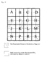
- peripheral pairs are C2D2, E2F2, C7D7, E7F7.
- the Occluded sensor positions of sensor 1A are:- A2B2C2D2, A3B3C3D3, A4B4C4D4, A5B5C5.
- a LED array provides the light source, which is collimated with the image through a lens onto the sensor array. This will allow selected LED's to be illuminated. If these LED's form an illuminated grid with arms that are a half resolution wide, that produces maximum white conditions on adjacent quarter resolution segments of adjacent row and column sensors, and the position of the network formed is moved by selecting different LED's for illumination, then four movements will identify the enhanced resolution grey scales.
- the fallout advantages are that using a lens for the LED array, will bring the mechanical tolerances within the capability of a qualified tradesman. By combining the two techniques, improvements of better than 4 times should now be feasible with minimum sampling. The use of a half resolution wide net should also reduce the effect of light contamination.
- Fig.8 shows a schematic of the arrangement.
- Figs.9 to Fig.12 show a 16 sensor array with the different positions of the Maximum White network (Light Mask) superimposed.
- Light Mask Maximum White network
Landscapes
- Engineering & Computer Science (AREA)
- Multimedia (AREA)
- Signal Processing (AREA)
- Facsimile Scanning Arrangements (AREA)
- Facsimile Heads (AREA)
- Transforming Light Signals Into Electric Signals (AREA)
Abstract
Description
- a. In this application of the invention, a Mask is positioned so that it occludes half of the light sensitive element of the array's non corner, peripheral sensors. This results in 3/4 of each of the 4 corner sensors being so occluded.
- b. The sensor array is displaced under the mask, with respect to the image, in the array's row axis (across) and column axis (down), by an amount equal to half the individual sensor's light sensitive element's dimensions, in the array's across, and down axis.
A2B2C2D2, A3B3C3D3, A4B4C4D4, A5B5C5.
Figs.9 to Fig.12 show a 16 sensor array with the different positions of the Maximum White network (Light Mask) superimposed.
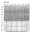
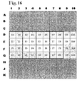
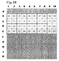
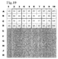
- a. Fig. 13 shows the start configuration. In each of the following diagrams ( Figs. 14 to 19), the image is successively advanced, relative to the sensor and mask, by a quarter resolution, and the position of the sensor is successively cycled to and fro, relative to the image and mask, by a quarter resolution in the mask's long axis.
- b. In Fig. 13, each of the array's end sensors have only four quarter resolution segments unmasked ( H3, H8,J3,J8 ). Each end sensor's charge is thus due to the image falling on its unmasked quarter resolution segment. This value is digitised and stored, as is the value of the remaining unmasked quarter resolution pairs (H4H5, H6H7, J4J5, and J6J7 ).
- c. In Fig 14, the image is advanced by a quarter resolution, relative to the mask and sensor, and the sensor is moved with respect to the image and mask by a quarter resolution. This means that the first two sensors of each row ( F1,F2,G1,G2 and H1,H2,J1,J2) are now masked, and the last two (F7,F8,G7,G8 and H7,H8,J7,J8 ) are half unmasked. The middle four sensors each have a pair of unmasked quarter resolution segments (G3,G4, and G5,G6) and ( H3,H4 and H5,H6). The digitised grey scale values of the unmasked quarter resolution segment pairs are stored. The image movement means row J is now masked and the grey scale values stored for this row will not be required
- d. Because H3 and H8 are known ( paragraph 18.f. above ), the values of H4,H5,H6,and H7, can be calculated by referring to the stored pair values ( paragraph 18.f. refers ), and entered on an Image quarter resolution Bit Map.
- e. Moving the image by a further quarter resolution, and returning the array to its original position relative to the mask, produces the situation shown in Fig. 15. The end sensors again now have only a quarter resolution segment exposed, so the values for these are now known ( F3,G3 - F8,G8 ) and stored. This allows the unknown quarter resolution segments ( G4,G5,G6,G7 ) to be calculated. The value of the remaining quarter resolution pairs are also stored.
- f. Repeating the process described above, allows a quarter resolution grey scale Bit Map to be constructed for the part of the image H3 to B8. which has been progressively exposed to the mask's window. Quarter resolution grey scale values for rows K and J are not calculable, and are ignored.
| How Each Quarter Resolution Segment Grey Scale Value Is Determined (para. 5i) | |||||
| Segment | Fictional Calculated Charge Value | Part of Pair or Group | Total Sensor Charge | Calculated From | Sensor Deflection |
| B2 fig.1 | 9 | 9) | (Only exposed | Neutral | |
| G2 fig.1 | 7 | 7) | (segments of each of | ||
| G7 fig.1 | 3 | 3) | (the corner sensors at | ||
| B7 fig.1 | 5 | 5) | (the Initial condition. | ||
| C2 fig.2 | 7 | B2+C2 | 16 | B2 known | Across |
| D2 fig.1 | 9 | C2+D2 | 16 | C2 calculated | Neutral |
| E2 fig.2 | 7 | D2+E2 | 16 | D2 calculated | Across |
| F2 or fig.1 | 7 | E2+F2 | 16 | E2 calculated | Neutral |
| F2 fig.2 | 7 | F2+G2 | 16 | G2 known | Across |
| C7 fig.2 | 3 | B7+C7 | 8 | B7 known | Across |
| D7 fig.1 | 5 | C7+D7 | 8 | C7 calculated | Neutral |
| E7 fig.2 | 3 | D7+E7 | 8 | D7 calculated | Across |
| F7 or fig.2 | 5 | F7+G7 | 8 | G7 known | Across |
| F7 fig.1 | 5 | E7+F7 | 8 | E7 calculated | Neutral |
| B3 fig.3 | 5 | B2+B3 | 14 | B2 known | Down |
| B4 fig.1 | 9 | B3+B4 | 14 | B3 calculated | Neutral |
| B5 fig.3 | 5 | B4+B5 | 14 | B4 calculated | Down |
| B6 fig.1 | 9 | B5+B6 | 14 | B5 calculated | Neutral |
| G3 fig.3 | 3 | G2+G3 | 10 | G2 known | Down |
| G4 fig.1 | 7 | G3+G4 | 10 | G3 calculated | Neutral |
| G5 fig.3 | 3 | G4+G5 | 10 | G4 calculated | Down |
| G6 fig.1 | 7 | G5+G6 | 10 | G5 calculated | Neutral |
| C3 fig.4 | 3 | B2B3C2C3 | 24 | C3 only unknown | All |
| F3 fig.4 | 5 | F2F3G2G3 | 24 | F3 only unknown | Across |
| C6 fig.4 | 7 | B6B7C6C7 | 24 | C6 only unknown | and |
| F6 fig.4 | 9 | F6F7G6G7 | 24 | F6 only unknown | Down |
| D3 fig.3 | 5 | C2C3D2D3 | 24 | D3 only unknown | Down |
| E3 fig.3 | 3 | E2E3F2F3 | 24 | E3 only unknown | Down |
| D6 fig.3 | 9 | C6C7D6D7 | 24 | D6 only unknown | Down |
| E6 fig.3 | 7 | E6E7F6F7 | 24 | E6 only unknown | Down |
| C4 fig.2 | 7 | B3C3B4C4 | 24 | C4 only unknown | Across |
| F4 fig.2 | 9 | F3G3F4G4 | 24 | F4 only unknown | Across |
| C5 fig.2 | 3 | B5C5B6C6 | 24 | C5 only unknown | Across |
| F5 fig.2 | 5 | F5G5F6G6 | 24 | F5 only unknown | Across |
| D4 fig.1 | 9 | C3D3C4D4 | 24 | D4 only unknown | neutral |
| D5 fig.1 | 5 | C5D5C6D6 | 24 | D5 only unknown | neutral |
| E4 fig.1 | 7 | E3E4F3F4 | 24 | E4 only unknown | neutral |
| E5 fig.1 | 3 | E5E6F5F6 | 24 | E5 only unknown | neutral |
Claims (6)
- A method of improving the resolution of an image scanning electronic sensor array having a plurality of light sensitive elements, the method comprising:introducing means between the sensor array and the image and positioning said means so as to partially affect selected sensors in the array,relative displacement of the sensor array with respect to said means,calculation of improved resolution grey scale values from the changes in the sensor array's output.
- The method of claim 1 in which said means is a mask adapted to partially oclud said sensor array.
- The method of claim 1, in which said means is a light source.
- An improved resolution image scanning device comprisingan electronic sensor array having a plurality of light sensitive elements,a means located between said sensor array and the image, said means being displacable relative to said sensor array and adapted to partially affect by its position selected sensors in the array,and calculation means for calculating improved resolution grey scale values from the changes in the sensor array's output.
- The device of claim 4, in which said means comprises a partially occluding mask.
- The device of claim 4, in which said means comprises a light source.
Priority Applications (1)
| Application Number | Priority Date | Filing Date | Title |
|---|---|---|---|
| EP01124155A EP1198119A3 (en) | 2000-10-11 | 2001-10-10 | Improved resolution for an electric image sensor array |
Applications Claiming Priority (5)
| Application Number | Priority Date | Filing Date | Title |
|---|---|---|---|
| EP00122032 | 2000-10-11 | ||
| EP00122032 | 2000-10-11 | ||
| EP00125188 | 2000-11-20 | ||
| EP00125188 | 2000-11-20 | ||
| EP01124155A EP1198119A3 (en) | 2000-10-11 | 2001-10-10 | Improved resolution for an electric image sensor array |
Publications (2)
| Publication Number | Publication Date |
|---|---|
| EP1198119A2 true EP1198119A2 (en) | 2002-04-17 |
| EP1198119A3 EP1198119A3 (en) | 2004-05-26 |
Family
ID=27223141
Family Applications (1)
| Application Number | Title | Priority Date | Filing Date |
|---|---|---|---|
| EP01124155A Withdrawn EP1198119A3 (en) | 2000-10-11 | 2001-10-10 | Improved resolution for an electric image sensor array |
Country Status (1)
| Country | Link |
|---|---|
| EP (1) | EP1198119A3 (en) |
Cited By (2)
| Publication number | Priority date | Publication date | Assignee | Title |
|---|---|---|---|---|
| WO2013171738A1 (en) | 2012-05-13 | 2013-11-21 | Elbit Systems Electro-Optics Elop Ltd. | Infrared detector with increased image resolution |
| WO2021224908A1 (en) | 2020-05-03 | 2021-11-11 | Elbit Systems Electro-Optics Elop Ltd | Systems and methods for enhanced motion detection, object tracking, situational awareness and super resolution video using microscanned images |
Family Cites Families (5)
| Publication number | Priority date | Publication date | Assignee | Title |
|---|---|---|---|---|
| JPH0682305A (en) * | 1992-08-31 | 1994-03-22 | Shimadzu Corp | Two-dimensional detector |
| CA2135676A1 (en) * | 1994-11-14 | 1996-05-15 | Jean Dumas | Device to enhance imaging resolution |
| US5900949A (en) * | 1996-05-23 | 1999-05-04 | Hewlett-Packard Company | CCD imager for confocal scanning microscopy |
| AUPO615297A0 (en) * | 1997-04-10 | 1997-05-08 | Commonwealth Scientific And Industrial Research Organisation | Imaging system and method |
| US6414760B1 (en) * | 1998-10-29 | 2002-07-02 | Hewlett-Packard Company | Image scanner with optical waveguide and enhanced optical sampling rate |
-
2001
- 2001-10-10 EP EP01124155A patent/EP1198119A3/en not_active Withdrawn
Cited By (5)
| Publication number | Priority date | Publication date | Assignee | Title |
|---|---|---|---|---|
| WO2013171738A1 (en) | 2012-05-13 | 2013-11-21 | Elbit Systems Electro-Optics Elop Ltd. | Infrared detector with increased image resolution |
| US9894292B2 (en) | 2012-05-13 | 2018-02-13 | Elbit Systems Electro-Optics Elop Ltd. | Infrared detector with increased image resolution and method for use thereof |
| US10547799B2 (en) | 2012-05-13 | 2020-01-28 | Elbit Systems Electro-Optics Elop Ltd. | Infrared detector with increased image resolution |
| WO2021224908A1 (en) | 2020-05-03 | 2021-11-11 | Elbit Systems Electro-Optics Elop Ltd | Systems and methods for enhanced motion detection, object tracking, situational awareness and super resolution video using microscanned images |
| US11861849B2 (en) | 2020-05-03 | 2024-01-02 | Elbit Systems Electro-Optics Elop Ltd | Systems and methods for enhanced motion detection, object tracking, situational awareness and super resolution video using microscanned images |
Also Published As
| Publication number | Publication date |
|---|---|
| EP1198119A3 (en) | 2004-05-26 |
Similar Documents
| Publication | Publication Date | Title |
|---|---|---|
| US6172352B1 (en) | Sensing module for accelerating signal readout from image sensors | |
| US4638371A (en) | Multiple exposure of area image sensor having a sparse array of elements | |
| US20020163582A1 (en) | Self-calibrating, digital, large format camera with single or mulitiple detector arrays and single or multiple optical systems | |
| JPH0739935B2 (en) | Image sensor | |
| EP0998114A2 (en) | Image scanner with optical waveguide and enhanced optical sampling rate | |
| CA2227289C (en) | Run-length encoded image rotation | |
| CN101706961A (en) | Image registration method and image registration device | |
| JP2915269B2 (en) | 3D camera image data processor | |
| EP0215847B1 (en) | Apparatus and method for forming digital images | |
| JP2010118818A (en) | Image capturing apparatus | |
| JP4342611B2 (en) | Improving image capture with push-bloom scanning | |
| SE427516B (en) | SET AND DEVICE FOR CORRECTING DISTORTION IN AN ELECTRONIC WAY RECORDED BY PICTURE ELEMENTS LONG LINES BUILDING PICTURE | |
| US6169576B1 (en) | Solid state image sensing device having variable resolution and color linear image sensor having variable resolution and control method thereof | |
| JPH11289485A (en) | Optical reconnaissance system | |
| US6115139A (en) | Readout system for a full-color image input scanner having three linear arrays of photosensors | |
| EP1168814A2 (en) | Image processing apparatus and processing method therefor | |
| EP1017240A3 (en) | Colour image signal generation | |
| US6593559B2 (en) | Image readout apparatus and image readout method using the same | |
| JPH0399574A (en) | Color image sensor | |
| RU2798768C1 (en) | Method of processing scan images | |
| AU759445B2 (en) | CCD readout method | |
| JPH06225187A (en) | Imaging device | |
| JP3481822B2 (en) | Solid-state imaging device and color linear image sensor | |
| TW580561B (en) | A method for measuring the perpendicularity between an image detector and its relative movement direction with an object detected | |
| JP2643770B2 (en) | Imaging device |
Legal Events
| Date | Code | Title | Description |
|---|---|---|---|
| PUAI | Public reference made under article 153(3) epc to a published international application that has entered the european phase |
Free format text: ORIGINAL CODE: 0009012 |
|
| AK | Designated contracting states |
Kind code of ref document: A2 Designated state(s): AT BE CH CY DE DK ES FI FR GB GR IE IT LI LU MC NL PT SE TR |
|
| AX | Request for extension of the european patent |
Free format text: AL;LT;LV;MK;RO;SI |
|
| PUAL | Search report despatched |
Free format text: ORIGINAL CODE: 0009013 |
|
| AK | Designated contracting states |
Kind code of ref document: A3 Designated state(s): AT BE CH CY DE DK ES FI FR GB GR IE IT LI LU MC NL PT SE TR |
|
| AX | Request for extension of the european patent |
Extension state: AL LT LV MK RO SI |
|
| 17P | Request for examination filed |
Effective date: 20041126 |
|
| AKX | Designation fees paid |
Designated state(s): AT BE CH CY DE DK ES FI FR GB GR IE IT LI LU MC NL PT SE TR |
|
| 17Q | First examination report despatched |
Effective date: 20050301 |
|
| STAA | Information on the status of an ep patent application or granted ep patent |
Free format text: STATUS: THE APPLICATION IS DEEMED TO BE WITHDRAWN |
|
| 18D | Application deemed to be withdrawn |
Effective date: 20060901 |