EP2835886B1 - Power supply module and soft start method - Google Patents
Power supply module and soft start method Download PDFInfo
- Publication number
- EP2835886B1 EP2835886B1 EP14158367.4A EP14158367A EP2835886B1 EP 2835886 B1 EP2835886 B1 EP 2835886B1 EP 14158367 A EP14158367 A EP 14158367A EP 2835886 B1 EP2835886 B1 EP 2835886B1
- Authority
- EP
- European Patent Office
- Prior art keywords
- power supply
- circuit
- supply module
- signal
- joint
- Prior art date
- Legal status (The legal status is an assumption and is not a legal conclusion. Google has not performed a legal analysis and makes no representation as to the accuracy of the status listed.)
- Active
Links
- 238000000034 method Methods 0.000 title claims description 20
- 238000001514 detection method Methods 0.000 claims description 148
- 239000003990 capacitor Substances 0.000 claims description 53
- 230000003287 optical effect Effects 0.000 claims description 23
- 238000010586 diagram Methods 0.000 description 14
- 230000035939 shock Effects 0.000 description 5
- 230000004044 response Effects 0.000 description 4
- 101100489713 Saccharomyces cerevisiae (strain ATCC 204508 / S288c) GND1 gene Proteins 0.000 description 3
- 101100489717 Saccharomyces cerevisiae (strain ATCC 204508 / S288c) GND2 gene Proteins 0.000 description 3
- 230000001419 dependent effect Effects 0.000 description 3
- 238000012986 modification Methods 0.000 description 3
- 230000004048 modification Effects 0.000 description 3
- 238000002955 isolation Methods 0.000 description 2
- 230000009286 beneficial effect Effects 0.000 description 1
- 230000008859 change Effects 0.000 description 1
- 238000004891 communication Methods 0.000 description 1
- 238000010891 electric arc Methods 0.000 description 1
- 238000005516 engineering process Methods 0.000 description 1
- 230000006870 function Effects 0.000 description 1
- 238000010438 heat treatment Methods 0.000 description 1
- 230000008569 process Effects 0.000 description 1
Images


Classifications
-
- H—ELECTRICITY
- H02—GENERATION; CONVERSION OR DISTRIBUTION OF ELECTRIC POWER
- H02H—EMERGENCY PROTECTIVE CIRCUIT ARRANGEMENTS
- H02H9/00—Emergency protective circuit arrangements for limiting excess current or voltage without disconnection
- H02H9/02—Emergency protective circuit arrangements for limiting excess current or voltage without disconnection responsive to excess current
-
- B—PERFORMING OPERATIONS; TRANSPORTING
- B60—VEHICLES IN GENERAL
- B60L—PROPULSION OF ELECTRICALLY-PROPELLED VEHICLES; SUPPLYING ELECTRIC POWER FOR AUXILIARY EQUIPMENT OF ELECTRICALLY-PROPELLED VEHICLES; ELECTRODYNAMIC BRAKE SYSTEMS FOR VEHICLES IN GENERAL; MAGNETIC SUSPENSION OR LEVITATION FOR VEHICLES; MONITORING OPERATING VARIABLES OF ELECTRICALLY-PROPELLED VEHICLES; ELECTRIC SAFETY DEVICES FOR ELECTRICALLY-PROPELLED VEHICLES
- B60L53/00—Methods of charging batteries, specially adapted for electric vehicles; Charging stations or on-board charging equipment therefor; Exchange of energy storage elements in electric vehicles
- B60L53/10—Methods of charging batteries, specially adapted for electric vehicles; Charging stations or on-board charging equipment therefor; Exchange of energy storage elements in electric vehicles characterised by the energy transfer between the charging station and the vehicle
- B60L53/14—Conductive energy transfer
- B60L53/18—Cables specially adapted for charging electric vehicles
-
- G—PHYSICS
- G05—CONTROLLING; REGULATING
- G05F—SYSTEMS FOR REGULATING ELECTRIC OR MAGNETIC VARIABLES
- G05F5/00—Systems for regulating electric variables by detecting deviations in the electric input to the system and thereby controlling a device within the system to obtain a regulated output
-
- H—ELECTRICITY
- H01—ELECTRIC ELEMENTS
- H01H—ELECTRIC SWITCHES; RELAYS; SELECTORS; EMERGENCY PROTECTIVE DEVICES
- H01H51/00—Electromagnetic relays
- H01H51/34—Self-interrupters, i.e. with periodic or other repetitive opening and closing of contacts
-
- H—ELECTRICITY
- H01—ELECTRIC ELEMENTS
- H01R—ELECTRICALLY-CONDUCTIVE CONNECTIONS; STRUCTURAL ASSOCIATIONS OF A PLURALITY OF MUTUALLY-INSULATED ELECTRICAL CONNECTING ELEMENTS; COUPLING DEVICES; CURRENT COLLECTORS
- H01R13/00—Details of coupling devices of the kinds covered by groups H01R12/70 or H01R24/00 - H01R33/00
- H01R13/64—Means for preventing incorrect coupling
- H01R13/641—Means for preventing incorrect coupling by indicating incorrect coupling; by indicating correct or full engagement
-
- H—ELECTRICITY
- H01—ELECTRIC ELEMENTS
- H01R—ELECTRICALLY-CONDUCTIVE CONNECTIONS; STRUCTURAL ASSOCIATIONS OF A PLURALITY OF MUTUALLY-INSULATED ELECTRICAL CONNECTING ELEMENTS; COUPLING DEVICES; CURRENT COLLECTORS
- H01R13/00—Details of coupling devices of the kinds covered by groups H01R12/70 or H01R24/00 - H01R33/00
- H01R13/66—Structural association with built-in electrical component
- H01R13/70—Structural association with built-in electrical component with built-in switch
- H01R13/713—Structural association with built-in electrical component with built-in switch the switch being a safety switch
-
- H—ELECTRICITY
- H01—ELECTRIC ELEMENTS
- H01R—ELECTRICALLY-CONDUCTIVE CONNECTIONS; STRUCTURAL ASSOCIATIONS OF A PLURALITY OF MUTUALLY-INSULATED ELECTRICAL CONNECTING ELEMENTS; COUPLING DEVICES; CURRENT COLLECTORS
- H01R29/00—Coupling parts for selective co-operation with a counterpart in different ways to establish different circuits, e.g. for voltage selection, for series-parallel selection, programmable connectors
-
- H—ELECTRICITY
- H02—GENERATION; CONVERSION OR DISTRIBUTION OF ELECTRIC POWER
- H02H—EMERGENCY PROTECTIVE CIRCUIT ARRANGEMENTS
- H02H3/00—Emergency protective circuit arrangements for automatic disconnection directly responsive to an undesired change from normal electric working condition with or without subsequent reconnection ; integrated protection
- H02H3/08—Emergency protective circuit arrangements for automatic disconnection directly responsive to an undesired change from normal electric working condition with or without subsequent reconnection ; integrated protection responsive to excess current
- H02H3/093—Emergency protective circuit arrangements for automatic disconnection directly responsive to an undesired change from normal electric working condition with or without subsequent reconnection ; integrated protection responsive to excess current with timing means
-
- H—ELECTRICITY
- H02—GENERATION; CONVERSION OR DISTRIBUTION OF ELECTRIC POWER
- H02H—EMERGENCY PROTECTIVE CIRCUIT ARRANGEMENTS
- H02H9/00—Emergency protective circuit arrangements for limiting excess current or voltage without disconnection
- H02H9/001—Emergency protective circuit arrangements for limiting excess current or voltage without disconnection limiting speed of change of electric quantities, e.g. soft switching on or off
- H02H9/002—Emergency protective circuit arrangements for limiting excess current or voltage without disconnection limiting speed of change of electric quantities, e.g. soft switching on or off limiting inrush current on switching on of inductive loads subjected to remanence, e.g. transformers
-
- H—ELECTRICITY
- H02—GENERATION; CONVERSION OR DISTRIBUTION OF ELECTRIC POWER
- H02H—EMERGENCY PROTECTIVE CIRCUIT ARRANGEMENTS
- H02H9/00—Emergency protective circuit arrangements for limiting excess current or voltage without disconnection
- H02H9/02—Emergency protective circuit arrangements for limiting excess current or voltage without disconnection responsive to excess current
- H02H9/025—Current limitation using field effect transistors
-
- B—PERFORMING OPERATIONS; TRANSPORTING
- B60—VEHICLES IN GENERAL
- B60L—PROPULSION OF ELECTRICALLY-PROPELLED VEHICLES; SUPPLYING ELECTRIC POWER FOR AUXILIARY EQUIPMENT OF ELECTRICALLY-PROPELLED VEHICLES; ELECTRODYNAMIC BRAKE SYSTEMS FOR VEHICLES IN GENERAL; MAGNETIC SUSPENSION OR LEVITATION FOR VEHICLES; MONITORING OPERATING VARIABLES OF ELECTRICALLY-PROPELLED VEHICLES; ELECTRIC SAFETY DEVICES FOR ELECTRICALLY-PROPELLED VEHICLES
- B60L2270/00—Problem solutions or means not otherwise provided for
- B60L2270/20—Inrush current reduction, i.e. avoiding high currents when connecting the battery
-
- B—PERFORMING OPERATIONS; TRANSPORTING
- B60—VEHICLES IN GENERAL
- B60L—PROPULSION OF ELECTRICALLY-PROPELLED VEHICLES; SUPPLYING ELECTRIC POWER FOR AUXILIARY EQUIPMENT OF ELECTRICALLY-PROPELLED VEHICLES; ELECTRODYNAMIC BRAKE SYSTEMS FOR VEHICLES IN GENERAL; MAGNETIC SUSPENSION OR LEVITATION FOR VEHICLES; MONITORING OPERATING VARIABLES OF ELECTRICALLY-PROPELLED VEHICLES; ELECTRIC SAFETY DEVICES FOR ELECTRICALLY-PROPELLED VEHICLES
- B60L53/00—Methods of charging batteries, specially adapted for electric vehicles; Charging stations or on-board charging equipment therefor; Exchange of energy storage elements in electric vehicles
- B60L53/10—Methods of charging batteries, specially adapted for electric vehicles; Charging stations or on-board charging equipment therefor; Exchange of energy storage elements in electric vehicles characterised by the energy transfer between the charging station and the vehicle
- B60L53/14—Conductive energy transfer
- B60L53/16—Connectors, e.g. plugs or sockets, specially adapted for charging electric vehicles
-
- G—PHYSICS
- G01—MEASURING; TESTING
- G01R—MEASURING ELECTRIC VARIABLES; MEASURING MAGNETIC VARIABLES
- G01R31/00—Arrangements for testing electric properties; Arrangements for locating electric faults; Arrangements for electrical testing characterised by what is being tested not provided for elsewhere
- G01R31/50—Testing of electric apparatus, lines, cables or components for short-circuits, continuity, leakage current or incorrect line connections
- G01R31/66—Testing of connections, e.g. of plugs or non-disconnectable joints
- G01R31/68—Testing of releasable connections, e.g. of terminals mounted on a printed circuit board
-
- H—ELECTRICITY
- H02—GENERATION; CONVERSION OR DISTRIBUTION OF ELECTRIC POWER
- H02H—EMERGENCY PROTECTIVE CIRCUIT ARRANGEMENTS
- H02H9/00—Emergency protective circuit arrangements for limiting excess current or voltage without disconnection
- H02H9/001—Emergency protective circuit arrangements for limiting excess current or voltage without disconnection limiting speed of change of electric quantities, e.g. soft switching on or off
- H02H9/004—Emergency protective circuit arrangements for limiting excess current or voltage without disconnection limiting speed of change of electric quantities, e.g. soft switching on or off in connection with live-insertion of plug-in units
-
- H—ELECTRICITY
- H03—ELECTRONIC CIRCUITRY
- H03K—PULSE TECHNIQUE
- H03K17/00—Electronic switching or gating, i.e. not by contact-making and –breaking
- H03K17/51—Electronic switching or gating, i.e. not by contact-making and –breaking characterised by the components used
- H03K17/78—Electronic switching or gating, i.e. not by contact-making and –breaking characterised by the components used using opto-electronic devices, i.e. light-emitting and photoelectric devices electrically- or optically-coupled
- H03K17/795—Electronic switching or gating, i.e. not by contact-making and –breaking characterised by the components used using opto-electronic devices, i.e. light-emitting and photoelectric devices electrically- or optically-coupled controlling bipolar transistors
- H03K17/7955—Electronic switching or gating, i.e. not by contact-making and –breaking characterised by the components used using opto-electronic devices, i.e. light-emitting and photoelectric devices electrically- or optically-coupled controlling bipolar transistors using phototransistors
-
- Y—GENERAL TAGGING OF NEW TECHNOLOGICAL DEVELOPMENTS; GENERAL TAGGING OF CROSS-SECTIONAL TECHNOLOGIES SPANNING OVER SEVERAL SECTIONS OF THE IPC; TECHNICAL SUBJECTS COVERED BY FORMER USPC CROSS-REFERENCE ART COLLECTIONS [XRACs] AND DIGESTS
- Y02—TECHNOLOGIES OR APPLICATIONS FOR MITIGATION OR ADAPTATION AGAINST CLIMATE CHANGE
- Y02T—CLIMATE CHANGE MITIGATION TECHNOLOGIES RELATED TO TRANSPORTATION
- Y02T10/00—Road transport of goods or passengers
- Y02T10/60—Other road transportation technologies with climate change mitigation effect
- Y02T10/70—Energy storage systems for electromobility, e.g. batteries
-
- Y—GENERAL TAGGING OF NEW TECHNOLOGICAL DEVELOPMENTS; GENERAL TAGGING OF CROSS-SECTIONAL TECHNOLOGIES SPANNING OVER SEVERAL SECTIONS OF THE IPC; TECHNICAL SUBJECTS COVERED BY FORMER USPC CROSS-REFERENCE ART COLLECTIONS [XRACs] AND DIGESTS
- Y02—TECHNOLOGIES OR APPLICATIONS FOR MITIGATION OR ADAPTATION AGAINST CLIMATE CHANGE
- Y02T—CLIMATE CHANGE MITIGATION TECHNOLOGIES RELATED TO TRANSPORTATION
- Y02T10/00—Road transport of goods or passengers
- Y02T10/60—Other road transportation technologies with climate change mitigation effect
- Y02T10/7072—Electromobility specific charging systems or methods for batteries, ultracapacitors, supercapacitors or double-layer capacitors
-
- Y—GENERAL TAGGING OF NEW TECHNOLOGICAL DEVELOPMENTS; GENERAL TAGGING OF CROSS-SECTIONAL TECHNOLOGIES SPANNING OVER SEVERAL SECTIONS OF THE IPC; TECHNICAL SUBJECTS COVERED BY FORMER USPC CROSS-REFERENCE ART COLLECTIONS [XRACs] AND DIGESTS
- Y02—TECHNOLOGIES OR APPLICATIONS FOR MITIGATION OR ADAPTATION AGAINST CLIMATE CHANGE
- Y02T—CLIMATE CHANGE MITIGATION TECHNOLOGIES RELATED TO TRANSPORTATION
- Y02T90/00—Enabling technologies or technologies with a potential or indirect contribution to GHG emissions mitigation
- Y02T90/10—Technologies relating to charging of electric vehicles
- Y02T90/14—Plug-in electric vehicles
Definitions
- the invention relates to the field of power electronic technology, and particularly to a power supply module and a soft start method.
- An inrush current protection circuit for a polyphaser alternating current power system may include a plurality of current limiting resistors, each of which is electrically coupled in series between a respective one of a plurality of phases of the polyphase alternating current power source and a respective input of a polyphase transformer rectifier unit.
- the circuit may also include a plurality of power switches, each of which is electrically coupled in parallel with a respective one of the current limiting resistors, such that when each of the power switches is closed, essentially no electrical current flows through the respective current limiting resistor.
- the circuit may also include a power switch controller configured to control each of the power switches to be open such that an inrush current passes through the respective current limiting resistor rather than the power switch, and to be closed after a time delay has passed.
- a power mixing apparatus for mixing current from a first and a second power rail includes a first enabling circuit to provide a first enabling signal, a second enabling circuit to provide a second enabling signal, a first inrush limiter to output a first current in response to the first enabling signal, a second inrush limiter to output a second current in response to the second enabling signal, a first open-circuiting circuit to decouple the first enabling circuit from the first inrush limiter when the first open-circuiting circuit is open-circuited, a second open-circuiting circuit to decouple the second enabling circuit from the second inrush limiter when the second open-circuiting circuit is open-circuited, a first isolation circuit to isolate the first inrush limiter from the second current, a second isolation circuit to isolate the second inrush limiter from the first current, and a direct-current converter to convert the first and the second current in response to the first enabling signal and in response to the second enabling signal.
- a power supply module such as an Alternating Current (AC)/Direct Current (DC) rectifier module and a DC/DC converter has been widely applied to the fields of communication, computer, automobile and home appliance.
- a DC bus in the power supply module circuit is generally connected to an electrolytic capacitor and other electronic devices.
- soft start of the DC bus is realized in a way of cooperating a structure of mechanical lock with long and short pins of a connector; and another is that the soft start of the DC bus is realized by connecting a current-limiting resistor connected in parallel with a switch device into the DC bus.
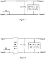
- the first solution is as shown in Figure 1 or Figure 2 , in which a current limiting resistor R1' is connected in one of two DC buses (the one of two DC buses may be the DC bus connected to an input terminal Input1 or may also be the DC bus connected to an input terminal Input2.
- the DC bus connected to the input terminal Input2 is taken as an example
- the resistor R1' is connected to a longer pin of the input terminals in the power supply module including the two DC buses.
- the power supply module When the power supply module is plugged into a power supply system which has been powered on, it can make sure that the longer pin of the input terminals in the power supply module first makes contact with the power supply system which has been powered on, and consequently the capacitor C1' between the two DC buses is charged via the current limiting resistor. The mechanical lock is then opened so that the power supply module is plugged into the right place completely. At that time, the longer pin connected to the resistor R1' is disconnected from the power supply system, and a pin of the input terminals in the power supply module which is connected to the input terminal Input2 is connected to the power supply system, and is connected to a pin in the output terminals of the power supply system which is in contact with the longer pin connected to the resistor R1' before the mechanical lock is opened.
- a difference between Figure 1 and Figure 2 is that signal input to the input terminal Input1 and the input terminal Input2 in Figure 1 is a DC signal, and signal input to the input terminal Input1 and the input terminal Input2 in Figure 2 is an AC signal, and the AC signal is converted into a DC signal via an AC/DC rectifier.
- a DC/AC converter or a DC/DC converter connected in parallel with the capacitor C1' is also included in Figure 1 and Figure 2 .
- a disadvantage of this solution is that, in this solution, first, the applying of delay is dependent on the structure of mechanical lock added to the power supply module, and since a duration of the delay is dependent on the capacitor C1' and the current limiting resistor R1', if the operation is too fast, there is a high difference between the voltage on the DC buses and the input DC voltage or the voltage of the DC signal obtained from the input AC signal after being rectified, which may also result in a big current shock and consequently result in damage to the electrolytic capacitor on the DC buses, and may damage the connection terminal connecting the power supply module including the DC buses and the power supply system. Therefore, it is apparent that the power supply module having such a structure has a high requirement on the skill of the operator.
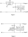
- a current limiting resistor R1' being connected in parallel with a switch device 31 is connected to a DC bus connected to an input terminal DC+ or a DC bus connected to an input terminal DC- (in Figure 3 , the DC bus connected to the input terminal DC+ is taken as an example).
- a current limiting resistor R1' being connected in parallel with the switch device 31 is connected in series with a branch circuit where a capacitor C1' is located.
- Each of the DC buses in Figure 3 and Figure 4 receives a DC signal.
- the second solution Compared with the first solution, in the second solution, no big inrush current will be generated whether when the power supply module is hot plugged or the power supply system including the power supply module is powered on.
- the second solution has disadvantages as follows. When the hot plug is performed repeatedly and if the operation is performed fast, the voltage on the DC bus in the power supply module will drop slowly after the power supply module is unplugged from the power supply system, and the power supply module is plugged into the power supply system fast again before the voltage drops to a shut-down determination voltage or a determination voltage for opening (turning off) the switch device.
- Embodiments of the present invention provide a power supply module and a soft start method, so as to solve the problem that when the existing power supply module is hot plugged rapidly on the power supply system, a big inrush current may be generated, which may damage the capacitor between the two DC buses and damage the connection terminal connecting the power supply module including the DC buses and the power supply system.
- an embodiment of the present invention provides a power supply module, including: DC buses, a current limiting circuit and a first capacitor, wherein the current limiting circuit is connected in a DC bus and the first capacitor is connected between two DC buses, or the current limiting circuit is connected between the two DC buses and then is connected in series with the first capacitor.
- the power supply module further includes a trigger drive circuit and an input detection circuit, wherein the input detection circuit is connected to the trigger drive circuit and the trigger drive circuit is then connected to the current limiting circuit.
- the input detection circuit is configured to output a first notification signal to the trigger drive circuit when it is determined that the power supply module begins to receive a power supply signal.
- the trigger drive circuit is configured to, upon receipt of the first notification signal sent from the input detection circuit, wait for a predetermined duration without sending a drive signal to the current limiting circuit, and to send the drive signal to the current limiting circuit when the predetermined duration elapses;
- the current limiting circuit is configured to limit a current on the DC buses when the drive signal is not received by the current limiting circuit, and not to limit the current on the DC bus when the drive signal is received by the current limiting circuit.
- An embodiment of the present invention provides a soft start method, including:
- the input detection circuit outputs a first notification signal to the trigger drive circuit when it is determined that the power supply module begins to receive a power supply signal, that is, the power supply module is plugged into the power supply system that has been powered on or the power supply system including the power supply module is started; upon receipt of the first notification signal, the trigger drive circuit waits for a predetermined duration without sending a drive signal to the current limiting circuit, so that the current limiting circuit limits a current on the DC bus(es) to avoid generating big current shock; and when the predetermined duration elapses, that is, when a voltage on the DC buses is close to a voltage of the power supply signal received by the power supply module, the trigger drive circuit sends the drive signal to the current limiting circuit, so that the current limiting circuit does not limit the current on the DC buses, thus realizing soft start of the power supply module.
- the embodiments of the present invention provides a power supply module and a soft start method in which a trigger drive circuit waits for a predetermined duration without sending a drive signal to a current limiting circuit upon receipt of a first notification signal, so that the current limiting circuit limits a current on the DC buses, and the trigger drive circuit sends the drive signal to the current limiting circuit when the predetermined duration elapses, so that the current limiting circuit no longer limits the current on the DC buses, thus realizing soft start of the power supply module, and solving the problem that when the power supply module is hot plugged rapidly on the power supply system, a big inrush current is generated, which may damage a capacitor between the two DC buses and damage a connection terminal connecting the power supply module including the DC buses and the power supply system.
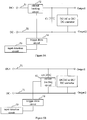
- the power supply module includes DC buses 51, a current limiting circuit 52, a first capacitor C1, a trigger drive circuit 54 and an input detection circuit 53.
- the current limiting circuit 52 is connected in a DC bus 51, and the first capacitor C1 is connected between two DC buses 51.
- the current limiting circuit 52 is connected in series with the first capacitor C1 and then is connected between the two DC buses 51, and the input detection circuit 53 is connected to the trigger drive circuit 54 and the trigger drive circuit 54 is then connected to the current limiting circuit 52.
- the input detection circuit 53 is configured to output a first notification signal to the trigger drive circuit 54 when it is determined that the power supply module begins to receive a power supply signal.
- the trigger drive circuit 54 is configured to wait for a predetermined duration without sending a drive signal to the current limiting circuit 52 when the first notification signal sent from the input detection circuit 53 is received, and to send the drive signal to the current limiting circuit 52 when the predetermined duration elapses.
- the current limiting circuit 52 is configured to limit a current on the DC buses 51 when the drive signal is not received, and not to limit the current on the DC buses 51 when the drive signal is received.
- a performance requirement for devices in the current limiting circuit 52 when the current limiting circuit 52 is connected in series in the branch circuit where the first capacitor C1 is located (as shown in Figure 5B ) is lower than a performance requirement for the devices in the current limiting circuit 52 when the current limiting circuit 52 is connected in series in a DC bus (as shown in Figure 5A ).
- a rated current of a device in the current limiting circuit 52 connected in series in the branch circuit where the first capacitor C1 is located is less than a rated current of the device in the current limiting 52 connected in series in the DC bus.
- the current limiting circuit 52 can employ a structure as shown in Figure 3 and Figure 4 in which a switch device is connected in parallel with a current limiting resistor.
- the switch device in the current limiting circuit 52 is opened when the current limiting circuit 52 has not received a drive signal sent from the trigger drive circuit 54, and thus a current flows through the current limiting resistor; and the switch device in the current limiting circuit is closed when the current limiting circuit 52 receives the drive signal sent from the trigger drive circuit 54, thus short-circuiting the current limiting resistor connected in parallel with the switch device, and a current flows through the closed switch device.
- the switch device may be a transistor, a relay or other controllable switch.
- the predetermined duration can be determined according to the first capacitor C1 and the current limiting resistor in the current limiting circuit. In order to avoid big current shock, the predetermined duration is generally not less than 10 times of a product of a value of the first capacitor C1 and a resistance value of the current limiting resistor.
- the input detection circuit 53 in the power supply module is further configured to output a second notification signal to the trigger drive circuit 54 when it is determined that the power supply module no longer receives the power supply signal; and the trigger drive circuit 54 is further configured not to send the drive signal to the current limiting circuit 52 when the second notification signal sent from the input detection circuit 53 is received, so that the current limiting circuit 52 limits the current on the DC buses 51.
- the connection terminals in the power supply module includes: a first detection joint 61 and a second detection joint 62, wherein each of the first detection joint 61 and the second detection joint 62 is connected to the input detection circuit 53; and other joints than the first detection joint 61 and the second detection joint 62 in the connection terminal of the power supply module when the first detection joint 61 and the second detection joint 62 are short-circuited by a short-circuit joint in the power supply system providing the power supply signal to the power supply module, such as a first power supply joint 63 and a second power supply joint 64, wherein the other joints are connected to corresponding joints in the connection terminal of the power supply system respectively.
- the first power supply joint 63 in the connection terminal of the power supply module is connected to one of the two DC buses in the power supply module
- the second power supply joint 64 in the connection terminal of the power supply module is connected to the other of the two DC buses in the power supply module.
- the input detection circuit determines whether the power supply module begins to receive the power supply signal, and then the input detection circuit outputs the first notification signal; and when the first detection joint 61 and the second detection joint 62 are disconnected, it is determined by the input detection circuit that the power supply module no longer receive the power supply signal, and then the input detection circuit outputs the second notification signal.
- the connection terminal of the power supply system shown in Figure 7 includes a first joint 71, a second joint 72 and a third joint 73.
- the first joint is the short-circuit joint, and the second joint 72 and the third joint 73 are configured to output the power supply signal to the power supply module.
- the first detection joint 61 and the second detection joint 62 being short-circuited by the short-circuit joint 71 in the power supply system means that each of the first detection joint 61 and the second detection joint 62 in the connection terminal of the power supply module is connected to the first joint 71 in the power supply system.
- the first detection joint 61 and the second detection joint 62 in the connection terminal of the power supply module can be short-circuited by the first joint 71 in the power supply system.
- the other joints than the first detection joint 61 and the second detection joint 62 in the connection terminal of the power supply module being connected to corresponding joints in the connection terminal of the power supply system respectively means that the first power supply joint 63 in the connection terminal of the power supply module is connected to the second joint 72 in the connection terminal of the power supply system and the second power supply joint 64 in the connection terminal of the power supply module is connected to the third joint 73 in the connection terminal of the power supply system.
- the length of each of the first detection joint 61 and the second detection joint 62 in the connection terminal of the power supply module provided by the embodiment of the present invention is less than the lengths of the other joints than the first detection joint 61 and the second detection joint 62 in the connection terminal of the power supply module.
- the first power supply joint 63 and the second power supply joint 64 are also included in Figure 8 . In this case, when the first detection joint 61 and the second detection joint 62 in the connection terminal of the power supply module are short-circuited by the short-circuit joint 71 in the connection terminal of the power supply system, the power supply module is connected to the power supply system reliably.
- connection terminal When such a connection terminal is employed, it can be avoided that a contact impedance between a joint in the connection terminal of the power supply module and a joint in the connection terminal of the power supply system in a case that the power supply module can operate normally when the power supply module is not connected to the power supply system reliably is greater than an impedance in a case that the power supply module is connected to the power supply system reliably.
- the loss of the connection terminal will increase much more than that in a normal connection, and the connection terminal will be damaged in severe heating.
- the first notification signal and the second notification signal output from the input detection circuit in the embodiment of the present invention have a difference between each other and the difference can be identified by the trigger drive circuit, that is, the trigger drive circuit can distinguish the first notification signal and the second notification signal.
- the first notification signal and the second notification signal may be digital signals, and the first notification signal is a high-level signal and the second notification signal is a low-level signal, or the first notification signal is a low-level signal and the second notification signal is a high-level signal.
- the first notification signal and the second notification signal may also be analog signals, and in this case, it is required that a difference between the first notification signal and the second notification signal can be identified by the trigger drive circuit.
- the difference between the first notification signal and the second notification signal may be a voltage difference, and may also be a current difference.
- the input detection circuit is illustrated by taking a case that the first notification signal and the second notification signal are digital signals, and the first notification signal is a low-level signal and the second notification signal is a high-level signal as an example.
- a case that the first notification signal is a high-level signal and the second notification signal is a low-level signal can be achieved by changing the connection relationship between devices.
- digital logic devices can be replaced with analog devices, and the first notification signal and the second notification signal can be distinguished by the trigger drive circuit using a difference between the first notification signal and the second notification signal.
- the input detection circuit in the power supply module provide in an embodiment of the present invention includes a first resistor R1, a second resistor R2, a second capacitor C2 and an optical coupler 91.
- One terminal of the first resistor R1 receives a first voltage signal V1.
- the other terminal of the first resistor R1 is connected to an anode of a light-emitting diode in the optical coupler 91.
- a cathode of the light-emitting diode in the optical coupler 91 is connected to the second detection joint 62.
- a collector of a phototransistor in the optical coupler 91 is connected to one terminal of the second resistor R2.
- the other terminal of the second resistor R2 receives a high-level signal.
- An emitter of the phototransistor in the optical coupler 91 receives a first ground signal GND1.
- One terminal of the second capacitor C2 is connected to the collector of the phototransistor in the optical coupler 91 and to the trigger drive circuit 54 respectively.
- the other terminal of the second capacitor C2 is connected to the emitter of the phototransistor in the optical coupler 91 and to the trigger drive circuit 54 respectively.
- the first detection joint 61 receives a second ground signal GND2.
- the first ground signal GND1 and the second ground signal GND2 may be the same ground signal or different ground signals.
- the interference of a signal received by the light-emitting diode in the optical coupler 91 to a signal received by the trigger drive circuit 54 can be prevented.
- the one terminal of the first resistor R1 receives the first voltage signal VI
- the other terminal of the first resistor R1 may also be connected to the cathode of the light-emitting diode in the optical coupler 91 and the anode of the light-emitting diode in the optical coupler 91 may be connected to the second detection joint 62. Which connection way is used can be determined by the polarity of the first voltage signal VI.
- the one terminal of the first resistor R1 receives the first voltage signal VI
- the other terminal of the first resistor R1 is connected to the anode of the light-emitting diode in the optical coupler 91
- the cathode of the light-emitting diode in the optical coupler 91 is connected to the second detection joint 62.
- the one terminal of the first resistor R1 receives the first voltage signal VI
- the other terminal of the first resistor R1 may also be connected to the cathode of the light-emitting diode in the optical coupler 91, and the anode of the light-emitting diode in the optical coupler 91 is connected to the second detection joint 62.
- the optical coupler 91 is configured to output a low-level signal to the trigger drive circuit 54 as the first notification signal when the first detection joint 61 and the second detection joint 62 are short-circuited by the short-circuit joint in the power supply system and thereby the light-emitting diode emits light and the conducting between the collector of the phototransistor and the emitter of the phototransistor is formed; and to output a high-level signal to the trigger drive circuit 54 as the second notification signal when the first detection joint 61 and the second detection joint 62 are disconnected and thereby the light-emitting does not emit light and the conducting between the collector of the phototransistor and the emitter of the phototransistor is broken.
- the input detection circuit of the power supply module provided by an embodiment of the present invention includes a third resistor R3, a fourth resistor R4, a third capacitor C3 and a transistor M1.
- One terminal of the third resistor R3 receives a second voltage signal V2.
- the other terminal of the third resistor R3 is connected to the second detection joint 62.
- a gate electrode of the transistor M1 is connected to the first detection joint 61.
- a first electrode of the transistor M1 is connected to one terminal of the fourth resistor R4.
- the other terminal of the fourth resistor R4 receives a high-level signal.
- a second electrode of the transistor M1 receives a third ground signal GND3.
- One terminal of the third capacitor C3 is connected to the first electrode of the transistor M1 and to the trigger drive circuit 54 respectively.
- the other terminal of the third capacitor C3 is connected to the second electrode of the transistor M1 and to the trigger drive circuit 54 respectively.
- the transistor M1 is configured to output a low-level signal to the trigger drive circuit 54 as the first notification signal when the first detection joint 61 and the second detection joint 62 are short-circuited by the short-circuit joint in the power supply system and thereby the conducting between the first electrode of the transistor M1 and the second electrode of the transistor M1 is formed; and to output a high-level signal to the trigger drive circuit 54 as the second notification signal when the first detection joint 61 and the second detection joint 62 are disconnected and thereby the conducting between the first electrode of the transistor and the second electrode of the transistor is broken.
- the second electrode of the transistor M1 is a drain electrode of the transistor M1.
- the first electrode of the transistor M1 is the drain electrode of the transistor M1
- the second electrode of the transistor M1 is the source electrode of the transistor M1.
- the current limiting circuit 52 is connected in the DC bus 51.
- the current limiting circuit 52 is connected between the two DC buses 51 after being connected in series with the capacitor C1.
- the input detection circuit in the power supply module provided by an embodiment of the present invention further includes a fifth resistor R5, a sixth resistor R6, a fourth capacitor C4 and a relay KM1.
- One terminal of the fifth resistor R5 receives a third voltage signal V3.
- the other terminal of the fifth resistor R5 is connected to one terminal of a coil in the relay KM1.
- the other terminal of the coil in the relay KM1 is connected to the second detection joint 62.
- One terminal of a normally open contact in the relay KM1 is connected to one terminal of the sixth resistor R6.
- the other terminal of the sixth resistor R6 receives a high-level signal.
- the other terminal of the normally open contact in the relay KM1 receives a fourth ground signal GND4.
- One terminal of the fourth capacitor C4 is connected to the one terminal of the normally open contact in the relay KM1 and to the trigger drive circuit 54 respectively.
- the other terminal of the fourth capacitor C4 is connected to the other terminal of the normally open contact in the relay KM1 and to the trigger drive circuit 54 respectively.
- the first detection joint 61 receives a fifth ground signal GND5.
- the relay KM1 is configured such that when the first detection joint 61 and the second detection joint 62 are short-circuited by the short-circuit joint in the power supply system, the normally open contact in the relay KM1 is closed, and thus a low-level signal is output to the trigger drive circuit 54 as the first notification signal; and when the first detection joint 61 and the second detection joint 62 are disconnected, the normally open contact in the relay KM1 is open, and thus a high-level signal is output to the trigger drive circuit 54 as the second notification signal.
- the current limiting circuit 52 is connected in the DC bus 51.
- the current limiting circuit 52 is connected between the two DC buses 51 after being connected in series with the capacitor C1.
- the fourth ground signal GND4 and the fifth ground signal GND5 may be the same ground signal, and may also be different ground signals.
- the fourth ground signal GND4 and the fifth ground signal GND5 are the different ground signals, the interference of a signal received by the coil in the relay KM1 to a signal received by the trigger drive circuit 54 can be prevented.
- the trigger drive circuit described above includes a DSP minimal system and a driver circuit.
- the DSP is configured to monitor whether the power supply signal has been received or the power supply signal is no longer received, and to realize a delay function.
- the driver circuit is configured to provide a drive signal to the switch device in the current limiting circuit.
- a soft start method provided by an embodiment of the present invention operates based upon the power supply module provided by an embodiment of the present invention.
- the principle for starting the power supply module provided by the embodiment of the present invention by means of this method is identical to the starting principle of the power supply module provided by the embodiment of the present invention, and the same part will not be repeated.
- the soft start method provided by an embodiment of the present invention further includes:
- the outputting, by an input detection circuit, a first notification signal to a trigger drive circuit when it is determined that the power supply module begins to receive a power supply signal includes:
- the power supply system shown in Figure 7 is employed as a power supply system, in the soft start method provided by the embodiment of the present invention, the outputting, by the input detection circuit, a second notification signal to the trigger drive circuit when it is determined that the power supply module no longer receives the power supply signal includes:
- the first notification signal output from the input detection circuit to the trigger drive circuit is a low-level signal
- the second notification signal output from the input detection circuit to the trigger drive circuit is a high-level signal
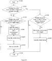
- the soft start method provided by the embodiment of the present invention can employ a flow shown in Figure 12 which includes the followings.
- step S 1200 it is started to perform a program related to the power supply module.
- step S1201 it is determined whether the power supply module is started and operates normally. If the power supply module is started and operates normally, a step S1202 is performed; otherwise, a step S1203 is performed.
- step S1202 it is determined whether the power supply module no longer receives the power supply signal. If the power supply module no longer receives the power supply signal, a step S1204 is performed; otherwise, the step S1209 is performed.
- step S1203 it is determined whether the power supply module begins to receive the power supply signal. If the power supply module begins to receive the power supply signal, a step S1206 is performed; otherwise, the step S1209 is performed.
- step S1204 a main power drive signal is shut down, and then a step S1205 is performed.
- step S1205 the switch device is open by shutting down the drive signal of the switch device in the current limiting circuit.
- step S1206 the switch device in the current limiting circuit is open, and a predetermined duration is waited for.
- step S1207 the drive signal is output to the switch device in the current limiting circuit when the predetermined duration elapses, so that the switch device is closed.
- step S1208 other start step such as a step of enabling the main power drive signal is performed.
- step S1209 the process related to the power supply module is completed.
- the step S1204 is performed first and then the step S1205 is performed.
- the inrush current can be prevented from being generated during a fast hot plug, but also a big ripple current can also be prevented from flowing through the current limiting resistor in the current limiting circuit during a slow hot plug.
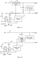
- Vin represents a signal on the first power supply joint or the second power supply joint of the power supply module.
- V_drv represents a drive signal of the main power switch device which is configured to control whether to output a power supply signal to a DC/AC converter or a DC/DC converter and a user load outside of the power supply module.
- V_plug represents the first notification signal and the second notification signal, and a low-level V_plug is the first notification signal and a high-level V_plug is the second notification signal.
- t b represents a time period between a time when the first detection joint and the second detection joint are disconnected and a time when the first power supply joint and the second power supply joint in the connection terminal of the power supply module are disconnected from the corresponding joints in the connection terminal of the power supply system.
- Vin represents a signal on the first power supply joint or the second power supply joint in the power supply module.
- V drv represents a drive signal of the main power switch device which is configured to control whether to output a power supply signal to a DC/AC converter or a DC/DC converter and a user load outside of the power supply module.
- V_plug represents the first notification signal and the second notification signal, and a low-level V_plug is the first notification signal and a high-level V_plug is the second notification signal.
- t a represents the predetermined duration.
- the first detection joint and the second detection joint are shorter than other joints in the connection terminal of the power supply module, when the power supply module is plugged into the power supply system, the first power supply joint and the second power supply joint in the connection terminal of the power supply module are first connected to the corresponding joints in the connection terminal of the power supply system, the first detection joint and the second detection joint are then connected to the short-circuit joint in the connection terminal of the power supply system, and the first detection joint and the second detection joint are short-circuited by the short-circuit joint.
- a time period between a time 0 and a time ta represents a time period between a time when the first power supply joint and the second power supply joint in the connection terminal of the power supply module are connected to the corresponding joints in the connection terminal of the power supply system and a time when the first detection joint and the second detection joint are connected to the short-circuit joint in the connection terminal of the power supply system.
- the embodiments of the present invention can be implemented by hardware, and can also be implemented by software with a necessary universal hardware platform.
- the technical solutions of the embodiments of the present invention can be embodied in a way of a software product, the software product may be stored in a non-volatile storage medium (which may be a Compact Disk-Read Only Memory (CD-ROM), a Universal Serial Bus (USB) or a mobile hard disk drive), and include multiple instructions to make a computer equipment (which may be a personal computer, a server or a network equipment) perform the method described in various embodiments of the present invention.
- a non-volatile storage medium which may be a Compact Disk-Read Only Memory (CD-ROM), a Universal Serial Bus (USB) or a mobile hard disk drive
- CD-ROM Compact Disk-Read Only Memory
- USB Universal Serial Bus
- a computer equipment which may be a personal computer, a server or a network equipment
- modules of the apparatus in the embodiment can be distributed in the apparatus of the embodiment according to the description of the embodiment, and can also be distributed in one or more apparatuses different from this embodiment by a corresponding change.
- the modules in the embodiment described above may be integrated into one module, and may also be further divided into multiple sub-modules.
Description
- The invention relates to the field of power electronic technology, and particularly to a power supply module and a soft start method.
-
US2011/058397 - An inrush current protection circuit for a polyphaser alternating current power system may include a plurality of current limiting resistors, each of which is electrically coupled in series between a respective one of a plurality of phases of the polyphase alternating current power source and a respective input of a polyphase transformer rectifier unit. The circuit may also include a plurality of power switches, each of which is electrically coupled in parallel with a respective one of the current limiting resistors, such that when each of the power switches is closed, essentially no electrical current flows through the respective current limiting resistor. The circuit may also include a power switch controller configured to control each of the power switches to be open such that an inrush current passes through the respective current limiting resistor rather than the power switch, and to be closed after a time delay has passed. -
EP0690554A2 - A power mixing apparatus for mixing current from a first and a second power rail includes a first enabling circuit to provide a first enabling signal, a second enabling circuit to provide a second enabling signal, a first inrush limiter to output a first current in response to the first enabling signal, a second inrush limiter to output a second current in response to the second enabling signal, a first open-circuiting circuit to decouple the first enabling circuit from the first inrush limiter when the first open-circuiting circuit is open-circuited, a second open-circuiting circuit to decouple the second enabling circuit from the second inrush limiter when the second open-circuiting circuit is open-circuited, a first isolation circuit to isolate the first inrush limiter from the second current, a second isolation circuit to isolate the second inrush limiter from the first current, and a direct-current converter to convert the first and the second current in response to the first enabling signal and in response to the second enabling signal. - A power supply module such as an Alternating Current (AC)/Direct Current (DC) rectifier module and a DC/DC converter has been widely applied to the fields of communication, computer, automobile and home appliance. A DC bus in the power supply module circuit is generally connected to an electrolytic capacitor and other electronic devices. When the power supply module connected to a power supply is started at the first time or when the power supply module is hot plugged on a power supply system, since a voltage on the DC bus in the power supply module does not necessarily reach a voltage resulted from an AC input after being rectified or a voltage of a DC input, a big current shock will be caused to the electrolytic capacitor connected to the DC bus, and the big current shock will result in damage to the electrolytic capacitor and occurrence of electric arc in a connection terminal connecting the power supply system and the power supply module, which may damage the connection terminal.
- For the above problems, there are two solutions in the prior art, one is that soft start of the DC bus is realized in a way of cooperating a structure of mechanical lock with long and short pins of a connector; and another is that the soft start of the DC bus is realized by connecting a current-limiting resistor connected in parallel with a switch device into the DC bus.
- The first solution is as shown in
Figure 1 or Figure 2 , in which a current limiting resistor R1' is connected in one of two DC buses (the one of two DC buses may be the DC bus connected to an input terminal Input1 or may also be the DC bus connected to an input terminal Input2. InFigure 1 and Figure 2 , the DC bus connected to the input terminal Input2 is taken as an example), the resistor R1' is connected to a longer pin of the input terminals in the power supply module including the two DC buses. When the power supply module is plugged into a power supply system which has been powered on, it can make sure that the longer pin of the input terminals in the power supply module first makes contact with the power supply system which has been powered on, and consequently the capacitor C1' between the two DC buses is charged via the current limiting resistor. The mechanical lock is then opened so that the power supply module is plugged into the right place completely. At that time, the longer pin connected to the resistor R1' is disconnected from the power supply system, and a pin of the input terminals in the power supply module which is connected to the input terminal Input2 is connected to the power supply system, and is connected to a pin in the output terminals of the power supply system which is in contact with the longer pin connected to the resistor R1' before the mechanical lock is opened. A difference betweenFigure 1 and Figure 2 is that signal input to the input terminal Input1 and the input terminal Input2 inFigure 1 is a DC signal, and signal input to the input terminal Input1 and the input terminal Input2 inFigure 2 is an AC signal, and the AC signal is converted into a DC signal via an AC/DC rectifier. A DC/AC converter or a DC/DC converter connected in parallel with the capacitor C1' is also included inFigure 1 and Figure 2 . If the DC/AC converter is connected in parallel with the capacitor C1' inFigure 1 and Figure 2 , an AC signal is output from the two output terminals Output1 and Output2 inFigure 1 and Figure 2 , and if the DC/DC converter is connected in parallel with the capacitor C1' inFigure 1 and Figure 2 , a DC signal is output from the two output terminals Output1 and Output2 inFigure 1 and Figure 2 . A disadvantage of this solution is that, in this solution, first, the applying of delay is dependent on the structure of mechanical lock added to the power supply module, and since a duration of the delay is dependent on the capacitor C1' and the current limiting resistor R1', if the operation is too fast, there is a high difference between the voltage on the DC buses and the input DC voltage or the voltage of the DC signal obtained from the input AC signal after being rectified, which may also result in a big current shock and consequently result in damage to the electrolytic capacitor on the DC buses, and may damage the connection terminal connecting the power supply module including the DC buses and the power supply system. Therefore, it is apparent that the power supply module having such a structure has a high requirement on the skill of the operator. In addition, if the power supply module has been plugged into the power supply system, a big inrush current will be generated when the power supply system is powered on, although which inrush current will not damage the connection terminal connecting the power supply module and the power supply system, but will damage the electrolytic capacitor on the DC buses. - The second solution is as shown in
Figure 3 or Figure 4 . InFigure 3 , a current limiting resistor R1' being connected in parallel with aswitch device 31 is connected to a DC bus connected to an input terminal DC+ or a DC bus connected to an input terminal DC- (inFigure 3 , the DC bus connected to the input terminal DC+ is taken as an example). InFigure 4 , a current limiting resistor R1' being connected in parallel with theswitch device 31 is connected in series with a branch circuit where a capacitor C1' is located. Each of the DC buses inFigure 3 and Figure 4 receives a DC signal. When a power supply module including the DC buses shown inFigure 3 or Figure 4 is plugged into a power supply system that has been powered on or when the power supply system into which the power supply module is plugged is powered on at the first time, the capacitor C1' in the DC buses is charged at first by the power supply module via the current limiting resistor R1'. When it is detected that a voltage on the DC bus reaches a predetermined value, theswitch device 31 is closed (turned on) to short-circuit the current limiting circuit R1' and a current flows through theswitch device 31. In this way, the current flows through the current limiting resistor R1' when the power supply module including the DC buses is powered on to start, and the current flows through the switch device during normal operation, thus realizing the purpose of soft start. Compared with the first solution, in the second solution, no big inrush current will be generated whether when the power supply module is hot plugged or the power supply system including the power supply module is powered on. However, the second solution has disadvantages as follows. When the hot plug is performed repeatedly and if the operation is performed fast, the voltage on the DC bus in the power supply module will drop slowly after the power supply module is unplugged from the power supply system, and the power supply module is plugged into the power supply system fast again before the voltage drops to a shut-down determination voltage or a determination voltage for opening (turning off) the switch device. Since there is a difference between the DC voltage output from the power supply system and the DC voltage on the DC buses of the power supply module, a big inrush current may be generated, which may damage the capacitor C1' between the two DC buses and may damage the connection terminal connecting the power supply module and the power supply system. - In conclusion, in a case that the existing DC bus structure is employed, when the power supply module including the DC buses is hot plugged rapidly on the power supply system, a big inrush current may be generated, which may damage the capacitor between the two DC buses and damage the connection terminal connecting the power supply module including the DC buses to the power supply system.
- Embodiments of the present invention provide a power supply module and a soft start method, so as to solve the problem that when the existing power supply module is hot plugged rapidly on the power supply system, a big inrush current may be generated, which may damage the capacitor between the two DC buses and damage the connection terminal connecting the power supply module including the DC buses and the power supply system.
- In view of the above problem, an embodiment of the present invention provides a power supply module, including: DC buses, a current limiting circuit and a first capacitor, wherein the current limiting circuit is connected in a DC bus and the first capacitor is connected between two DC buses, or the current limiting circuit is connected between the two DC buses and then is connected in series with the first capacitor. The power supply module further includes a trigger drive circuit and an input detection circuit, wherein the input detection circuit is connected to the trigger drive circuit and the trigger drive circuit is then connected to the current limiting circuit.
- The input detection circuit is configured to output a first notification signal to the trigger drive circuit when it is determined that the power supply module begins to receive a power supply signal.
- The trigger drive circuit is configured to, upon receipt of the first notification signal sent from the input detection circuit, wait for a predetermined duration without sending a drive signal to the current limiting circuit, and to send the drive signal to the current limiting circuit when the predetermined duration elapses; and
- The current limiting circuit is configured to limit a current on the DC buses when the drive signal is not received by the current limiting circuit, and not to limit the current on the DC bus when the drive signal is received by the current limiting circuit.
- An embodiment of the present invention provides a soft start method, including:
- outputting, by an input detection circuit, a first notification signal to a trigger drive circuit when it is determined that a power supply module begins to receive a power supply signal;
- waiting for a predetermined duration without sending a drive signal to a current limiting circuit by the trigger drive circuit when the first notification signal sent by the input detection circuit is received by the trigger drive circuit, and sending, by the trigger drive circuit, the drive signal to the current limiting circuit when the predetermined duration elapses; and
- limiting, by the current limiting circuit, a current on the DC buses when the drive signal is not received by the current limiting circuit, and not limiting, by the current limiting circuit, the current on the DC bus when the drive signal is received by the current limiting circuit.
- The beneficial effect of the embodiment of the present invention is as follows.
- In the power supply module and the soft start method provided by the embodiments of the present invention, the input detection circuit outputs a first notification signal to the trigger drive circuit when it is determined that the power supply module begins to receive a power supply signal, that is, the power supply module is plugged into the power supply system that has been powered on or the power supply system including the power supply module is started; upon receipt of the first notification signal, the trigger drive circuit waits for a predetermined duration without sending a drive signal to the current limiting circuit, so that the current limiting circuit limits a current on the DC bus(es) to avoid generating big current shock; and when the predetermined duration elapses, that is, when a voltage on the DC buses is close to a voltage of the power supply signal received by the power supply module, the trigger drive circuit sends the drive signal to the current limiting circuit, so that the current limiting circuit does not limit the current on the DC buses, thus realizing soft start of the power supply module. Hence, the following problem can be solved: when the existing power supply module is hot plugged rapidly on the power supply system, a big inrush current may be generated, which may damage the capacitor between the two DC buses and damage the connection terminal connecting the power supply module including the DC buses and the power supply system.
The present invention is set out in the independent claims with some optional features set out in the claims dependent thereto. -
-
Figures 1 to 4 are schematic structural diagrams of power supply modules in the prior art; -
Figure 5A is a first schematic structural diagram of a power supply module provided by an embodiment of the present invention; -
Figure 5B is a second schematic structural diagram of a power supply module provided by an embodiment of the present invention; -
Figure 6 is a first schematic structural diagram of a connection terminal of a power supply module provided by an embodiment of the present invention; -
Figure 7 is a schematic structural diagram of a connection terminal of a power supply system provided by an embodiment of the present invention; -
Figure 8 is a second schematic structural diagram of a connection terminal of a power supply module provided by an embodiment of the present invention; -
Figure 9A is a third schematic structural diagram of a power supply module provided by an embodiment of the present invention; -
Figure 9B is a fourth schematic structural diagram of a power supply module provided by an embodiment of the present invention; -
Figure 10A is a fifth schematic structural diagram of a power supply module provided by an embodiment of the present invention; -
Figure 10B is a sixth schematic structural diagram of a power supply module provided by an embodiment of the present invention; -
Figure 11A is a seventh schematic structural diagram of a power supply module provided by an embodiment of the present invention; -
Figure 11B is an eighth schematic structural diagram of a power supply module provided by an embodiment of the present invention; -
Figure 12 is a flow chart of a soft start method provided by an embodiment of the present invention in a practical application; and -
Figures 13 to 14 are schematic diagrams of signals at respective points of a power supply module provided by an embodiment of the present invention in a practical application. - The embodiments of the present invention provides a power supply module and a soft start method in which a trigger drive circuit waits for a predetermined duration without sending a drive signal to a current limiting circuit upon receipt of a first notification signal, so that the current limiting circuit limits a current on the DC buses, and the trigger drive circuit sends the drive signal to the current limiting circuit when the predetermined duration elapses, so that the current limiting circuit no longer limits the current on the DC buses, thus realizing soft start of the power supply module, and solving the problem that when the power supply module is hot plugged rapidly on the power supply system, a big inrush current is generated, which may damage a capacitor between the two DC buses and damage a connection terminal connecting the power supply module including the DC buses and the power supply system.
- A specific embodiment of the power supply module and the soft start method provided by the embodiments of the present invention will be illustrated below in conjunction with the accompanying drawings.
- An embodiment of the present invention provides a power supply module. As shown in
Figure 5A and Figure 5B , the power supply module includesDC buses 51, a current limitingcircuit 52, a first capacitor C1, atrigger drive circuit 54 and aninput detection circuit 53. InFigure 5A , the current limitingcircuit 52 is connected in aDC bus 51, and the first capacitor C1 is connected between twoDC buses 51. InFigure 5B , the current limitingcircuit 52 is connected in series with the first capacitor C1 and then is connected between the twoDC buses 51, and theinput detection circuit 53 is connected to thetrigger drive circuit 54 and thetrigger drive circuit 54 is then connected to the current limitingcircuit 52. - The
input detection circuit 53 is configured to output a first notification signal to thetrigger drive circuit 54 when it is determined that the power supply module begins to receive a power supply signal. - The
trigger drive circuit 54 is configured to wait for a predetermined duration without sending a drive signal to the current limitingcircuit 52 when the first notification signal sent from theinput detection circuit 53 is received, and to send the drive signal to the current limitingcircuit 52 when the predetermined duration elapses. - The current limiting
circuit 52 is configured to limit a current on theDC buses 51 when the drive signal is not received, and not to limit the current on theDC buses 51 when the drive signal is received. - In a case that the current limiting
circuit 52 is connected in series with the first capacitor C1 and then is connected between the twoDC buses 51, since a current in a branch circuit where the first capacitor C1 is located is less than a current on theDC buses 51, a performance requirement for devices in the current limitingcircuit 52 when the current limitingcircuit 52 is connected in series in the branch circuit where the first capacitor C1 is located (as shown inFigure 5B ) is lower than a performance requirement for the devices in the current limitingcircuit 52 when the current limitingcircuit 52 is connected in series in a DC bus (as shown inFigure 5A ). For example, a rated current of a device in the current limitingcircuit 52 connected in series in the branch circuit where the first capacitor C1 is located is less than a rated current of the device in the current limiting 52 connected in series in the DC bus. - Here the current limiting
circuit 52 can employ a structure as shown inFigure 3 and Figure 4 in which a switch device is connected in parallel with a current limiting resistor. In such case, the switch device in the current limitingcircuit 52 is opened when the current limitingcircuit 52 has not received a drive signal sent from thetrigger drive circuit 54, and thus a current flows through the current limiting resistor; and the switch device in the current limiting circuit is closed when the current limitingcircuit 52 receives the drive signal sent from thetrigger drive circuit 54, thus short-circuiting the current limiting resistor connected in parallel with the switch device, and a current flows through the closed switch device. The switch device may be a transistor, a relay or other controllable switch. - The predetermined duration can be determined according to the first capacitor C1 and the current limiting resistor in the current limiting circuit. In order to avoid big current shock, the predetermined duration is generally not less than 10 times of a product of a value of the first capacitor C1 and a resistance value of the current limiting resistor.
- Furthermore, the
input detection circuit 53 in the power supply module provided by an embodiment of the present invention is further configured to output a second notification signal to thetrigger drive circuit 54 when it is determined that the power supply module no longer receives the power supply signal; and thetrigger drive circuit 54 is further configured not to send the drive signal to the current limitingcircuit 52 when the second notification signal sent from theinput detection circuit 53 is received, so that the current limitingcircuit 52 limits the current on theDC buses 51. - Furthermore, as shown in
Figure 6 , the connection terminals in the power supply module provided by an embodiment of the present invention includes: a first detection joint 61 and a second detection joint 62, wherein each of the first detection joint 61 and the second detection joint 62 is connected to theinput detection circuit 53; and other joints than the first detection joint 61 and the second detection joint 62 in the connection terminal of the power supply module when the first detection joint 61 and the second detection joint 62 are short-circuited by a short-circuit joint in the power supply system providing the power supply signal to the power supply module, such as a firstpower supply joint 63 and a second power supply joint 64, wherein the other joints are connected to corresponding joints in the connection terminal of the power supply system respectively. The first power supply joint 63 in the connection terminal of the power supply module is connected to one of the two DC buses in the power supply module, and the second power supply joint 64 in the connection terminal of the power supply module is connected to the other of the two DC buses in the power supply module. - When the first detection joint 61 and the second detection joint 62 are short-circuited by the short-circuit joint in the connection terminal of the power supply system, it is determined by the input detection circuit that the power supply module begins to receive the power supply signal, and then the input detection circuit outputs the first notification signal; and when the first detection joint 61 and the second detection joint 62 are disconnected, it is determined by the input detection circuit that the power supply module no longer receive the power supply signal, and then the input detection circuit outputs the second notification signal.
- The connection terminal of the power supply system shown in
Figure 7 includes a first joint 71, a second joint 72 and a third joint 73. The first joint is the short-circuit joint, and the second joint 72 and the third joint 73 are configured to output the power supply signal to the power supply module. - When the power supply module provided by the embodiment of the present invention is plugged into the power supply system shown in
Figure 7 , the first detection joint 61 and the second detection joint 62 being short-circuited by the short-circuit joint 71 in the power supply system means that each of the first detection joint 61 and the second detection joint 62 in the connection terminal of the power supply module is connected to the first joint 71 in the power supply system. In this case, the first detection joint 61 and the second detection joint 62 in the connection terminal of the power supply module can be short-circuited by the first joint 71 in the power supply system. The other joints than the first detection joint 61 and the second detection joint 62 in the connection terminal of the power supply module being connected to corresponding joints in the connection terminal of the power supply system respectively means that the first power supply joint 63 in the connection terminal of the power supply module is connected to the second joint 72 in the connection terminal of the power supply system and the second power supply joint 64 in the connection terminal of the power supply module is connected to the third joint 73 in the connection terminal of the power supply system. - Furthermore, as shown in
Figure 8 , the length of each of the first detection joint 61 and the second detection joint 62 in the connection terminal of the power supply module provided by the embodiment of the present invention is less than the lengths of the other joints than the first detection joint 61 and the second detection joint 62 in the connection terminal of the power supply module. The firstpower supply joint 63 and the second power supply joint 64 are also included inFigure 8 . In this case, when the first detection joint 61 and the second detection joint 62 in the connection terminal of the power supply module are short-circuited by the short-circuit joint 71 in the connection terminal of the power supply system, the power supply module is connected to the power supply system reliably. When such a connection terminal is employed, it can be avoided that a contact impedance between a joint in the connection terminal of the power supply module and a joint in the connection terminal of the power supply system in a case that the power supply module can operate normally when the power supply module is not connected to the power supply system reliably is greater than an impedance in a case that the power supply module is connected to the power supply system reliably. When the power supply module is heavily loaded, the loss of the connection terminal will increase much more than that in a normal connection, and the connection terminal will be damaged in severe heating. - It is required that the first notification signal and the second notification signal output from the input detection circuit in the embodiment of the present invention have a difference between each other and the difference can be identified by the trigger drive circuit, that is, the trigger drive circuit can distinguish the first notification signal and the second notification signal. For example, the first notification signal and the second notification signal may be digital signals, and the first notification signal is a high-level signal and the second notification signal is a low-level signal, or the first notification signal is a low-level signal and the second notification signal is a high-level signal. The first notification signal and the second notification signal may also be analog signals, and in this case, it is required that a difference between the first notification signal and the second notification signal can be identified by the trigger drive circuit. The difference between the first notification signal and the second notification signal may be a voltage difference, and may also be a current difference.
- In the following, a specific embodiment of the input detection circuit is illustrated by taking a case that the first notification signal and the second notification signal are digital signals, and the first notification signal is a low-level signal and the second notification signal is a high-level signal as an example. In practice, of course, a case that the first notification signal is a high-level signal and the second notification signal is a low-level signal can be achieved by changing the connection relationship between devices. Also, digital logic devices can be replaced with analog devices, and the first notification signal and the second notification signal can be distinguished by the trigger drive circuit using a difference between the first notification signal and the second notification signal.
- As shown in
Figure 9A and Figure 9B , the input detection circuit in the power supply module provide in an embodiment of the present invention includes a first resistor R1, a second resistor R2, a second capacitor C2 and anoptical coupler 91. - One terminal of the first resistor R1 receives a first voltage signal V1. The other terminal of the first resistor R1 is connected to an anode of a light-emitting diode in the
optical coupler 91. A cathode of the light-emitting diode in theoptical coupler 91 is connected to thesecond detection joint 62. A collector of a phototransistor in theoptical coupler 91 is connected to one terminal of the second resistor R2. The other terminal of the second resistor R2 receives a high-level signal. An emitter of the phototransistor in theoptical coupler 91 receives a first ground signal GND1. One terminal of the second capacitor C2 is connected to the collector of the phototransistor in theoptical coupler 91 and to thetrigger drive circuit 54 respectively. The other terminal of the second capacitor C2 is connected to the emitter of the phototransistor in theoptical coupler 91 and to thetrigger drive circuit 54 respectively. The first detection joint 61 receives a second ground signal GND2. - The first ground signal GND1 and the second ground signal GND2 may be the same ground signal or different ground signals. When the first ground signal GND1 and the second ground signal GND2 are the different ground signals, the interference of a signal received by the light-emitting diode in the
optical coupler 91 to a signal received by thetrigger drive circuit 54 can be prevented. - In the
Figure 9A and Figure 9B , the one terminal of the first resistor R1 receives the first voltage signal VI, and the other terminal of the first resistor R1 may also be connected to the cathode of the light-emitting diode in theoptical coupler 91 and the anode of the light-emitting diode in theoptical coupler 91 may be connected to thesecond detection joint 62. Which connection way is used can be determined by the polarity of the first voltage signal VI. When the first voltage signal VI is a positive voltage signal, the one terminal of the first resistor R1 receives the first voltage signal VI, the other terminal of the first resistor R1 is connected to the anode of the light-emitting diode in theoptical coupler 91, and the cathode of the light-emitting diode in theoptical coupler 91 is connected to thesecond detection joint 62. When the first voltage signal VI is a negative voltage signal, the one terminal of the first resistor R1 receives the first voltage signal VI, the other terminal of the first resistor R1 may also be connected to the cathode of the light-emitting diode in theoptical coupler 91, and the anode of the light-emitting diode in theoptical coupler 91 is connected to thesecond detection joint 62. - The
optical coupler 91 is configured to output a low-level signal to thetrigger drive circuit 54 as the first notification signal when the first detection joint 61 and the second detection joint 62 are short-circuited by the short-circuit joint in the power supply system and thereby the light-emitting diode emits light and the conducting between the collector of the phototransistor and the emitter of the phototransistor is formed; and to output a high-level signal to thetrigger drive circuit 54 as the second notification signal when the first detection joint 61 and the second detection joint 62 are disconnected and thereby the light-emitting does not emit light and the conducting between the collector of the phototransistor and the emitter of the phototransistor is broken. - In
Figure 9A , the current limitingcircuit 52 is connected in aDC bus 51, and inFigure 9B , the current limitingcircuit 52 being connected in series with the capacitor C1 is connected between the twoDC buses 51. - Furthermore, as shown in
Figure 10A and 10B , the input detection circuit of the power supply module provided by an embodiment of the present invention includes a third resistor R3, a fourth resistor R4, a third capacitor C3 and a transistor M1. - One terminal of the third resistor R3 receives a second voltage signal V2. The other terminal of the third resistor R3 is connected to the
second detection joint 62. A gate electrode of the transistor M1 is connected to thefirst detection joint 61. A first electrode of the transistor M1 is connected to one terminal of the fourth resistor R4. The other terminal of the fourth resistor R4 receives a high-level signal. A second electrode of the transistor M1 receives a third ground signal GND3. One terminal of the third capacitor C3 is connected to the first electrode of the transistor M1 and to thetrigger drive circuit 54 respectively. The other terminal of the third capacitor C3 is connected to the second electrode of the transistor M1 and to thetrigger drive circuit 54 respectively. - The transistor M1 is configured to output a low-level signal to the
trigger drive circuit 54 as the first notification signal when the first detection joint 61 and the second detection joint 62 are short-circuited by the short-circuit joint in the power supply system and thereby the conducting between the first electrode of the transistor M1 and the second electrode of the transistor M1 is formed; and to output a high-level signal to thetrigger drive circuit 54 as the second notification signal when the first detection joint 61 and the second detection joint 62 are disconnected and thereby the conducting between the first electrode of the transistor and the second electrode of the transistor is broken. - When the first electrode of the transistor M1 is a source electrode of the transistor M1, the second electrode of the transistor M1 is a drain electrode of the transistor M1. When the first electrode of the transistor M1 is the drain electrode of the transistor M1, the second electrode of the transistor M1 is the source electrode of the transistor M1.
- In
Figure 10A , the current limitingcircuit 52 is connected in theDC bus 51. InFigure 10B , the current limitingcircuit 52 is connected between the twoDC buses 51 after being connected in series with the capacitor C1. - Furthermore, as shown in
Figure 11A and Figure 11B , the input detection circuit in the power supply module provided by an embodiment of the present invention further includes a fifth resistor R5, a sixth resistor R6, a fourth capacitor C4 and a relay KM1. - One terminal of the fifth resistor R5 receives a third voltage signal V3. The other terminal of the fifth resistor R5 is connected to one terminal of a coil in the relay KM1. The other terminal of the coil in the relay KM1 is connected to the
second detection joint 62. One terminal of a normally open contact in the relay KM1 is connected to one terminal of the sixth resistor R6. The other terminal of the sixth resistor R6 receives a high-level signal. The other terminal of the normally open contact in the relay KM1 receives a fourth ground signal GND4. One terminal of the fourth capacitor C4 is connected to the one terminal of the normally open contact in the relay KM1 and to thetrigger drive circuit 54 respectively. The other terminal of the fourth capacitor C4 is connected to the other terminal of the normally open contact in the relay KM1 and to thetrigger drive circuit 54 respectively. The first detection joint 61 receives a fifth ground signal GND5. - The relay KM1 is configured such that when the first detection joint 61 and the second detection joint 62 are short-circuited by the short-circuit joint in the power supply system, the normally open contact in the relay KM1 is closed, and thus a low-level signal is output to the
trigger drive circuit 54 as the first notification signal; and when the first detection joint 61 and the second detection joint 62 are disconnected, the normally open contact in the relay KM1 is open, and thus a high-level signal is output to thetrigger drive circuit 54 as the second notification signal. - In
Figure 11A , the current limitingcircuit 52 is connected in theDC bus 51. InFigure 11B , the current limitingcircuit 52 is connected between the twoDC buses 51 after being connected in series with the capacitor C1. - The fourth ground signal GND4 and the fifth ground signal GND5 may be the same ground signal, and may also be different ground signals. When the fourth ground signal GND4 and the fifth ground signal GND5 are the different ground signals, the interference of a signal received by the coil in the relay KM1 to a signal received by the
trigger drive circuit 54 can be prevented. - The trigger drive circuit described above includes a DSP minimal system and a driver circuit. The DSP is configured to monitor whether the power supply signal has been received or the power supply signal is no longer received, and to realize a delay function. The driver circuit is configured to provide a drive signal to the switch device in the current limiting circuit.
- A soft start method provided by an embodiment of the present invention operates based upon the power supply module provided by an embodiment of the present invention. The principle for starting the power supply module provided by the embodiment of the present invention by means of this method is identical to the starting principle of the power supply module provided by the embodiment of the present invention, and the same part will not be repeated.
- The soft start method provided by the embodiment of the present invention includes:
- outputting, by an input detection circuit, a first notification signal to a trigger drive circuit when it is determined that the power supply module begins to receive a power supply signal;
- waiting for a predetermined duration without sending a drive signal to a current limiting circuit by the trigger drive circuit when the first notification signal sent from the input detection circuit is received; and sending, by the trigger drive circuit, the drive signal to the current limiting circuit when the predetermined duration elapses; and
- limiting, by the current limiting circuit, a current on a DC bus when the drive signal is not received; and not limiting, by the current limiting circuit, the current on the DC bus when the drive signal is received.
- Furthermore, the soft start method provided by an embodiment of the present invention further includes:
- outputting, by the input detection circuit, a second notification signal to the trigger drive module when it is determined that the power supply module no longer receives the power supply signal; and
- not sending, by the trigger drive circuit, the drive signal to the current limiting circuit when the second notification signal sent from the input detection circuit has been received, so that the current limiting circuit limits the current on the DC bus.
- Furthermore, when any power supply module shown in
Figure 6, Figure 8 ,Figure 9A, Figure 9B ,Figure 10A, Figure 10B ,Figure 11A and Figure 11B is employed as the power supply module provided by the embodiment of the present invention and the power supply system shown inFigure 7 is employed as a power supply system, in the soft start method provided by the embodiment of the present invention, the outputting, by an input detection circuit, a first notification signal to a trigger drive circuit when it is determined that the power supply module begins to receive a power supply signal includes: - determining, by the input detection circuit, that the power supply module begins to receive the power supply signal when the first detection joint and the second detection joint are short-circuited by a short-circuit joint in the power supply system; and
- outputting, by the input detection circuit, the first notification signal to the trigger drive circuit.
- Furthermore, when any power supply module shown in
Figure 6, Figure 8 ,Figure 9A, Figure 9B ,Figure 10A, Figure 10B ,Figure 11A and Figure 11B is employed as the power supply module provided by the embodiment of the present invention the power supply system shown inFigure 7 is employed as a power supply system, in the soft start method provided by the embodiment of the present invention, the outputting, by the input detection circuit, a second notification signal to the trigger drive circuit when it is determined that the power supply module no longer receives the power supply signal includes: - determining, by the input detection circuit, that the power supply module no longer receives the power supply signal when the first detection joint and the second detection joint are disconnected; and
- outputting, by the input detection circuit, the second notification signal to the trigger drive circuit.
- Furthermore, when any power supply module shown in
Figure 9A, Figure 9B ,Figure 10A, Figure 10B ,Figure 11A and Figure 11B is employed as the power supply module provided by the embodiment of the present invention, the first notification signal output from the input detection circuit to the trigger drive circuit is a low-level signal, and the second notification signal output from the input detection circuit to the trigger drive circuit is a high-level signal. - Furthermore, in practical application, the soft start method provided by the embodiment of the present invention can employ a flow shown in
Figure 12 which includes the followings. - In
step S 1200, it is started to perform a program related to the power supply module. - In step S1201, it is determined whether the power supply module is started and operates normally. If the power supply module is started and operates normally, a step S1202 is performed; otherwise, a step S1203 is performed.
- In step S1202, it is determined whether the power supply module no longer receives the power supply signal. If the power supply module no longer receives the power supply signal, a step S1204 is performed; otherwise, the step S1209 is performed.
- In step S1203, it is determined whether the power supply module begins to receive the power supply signal. If the power supply module begins to receive the power supply signal, a step S1206 is performed; otherwise, the step S1209 is performed.
- In step S1204, a main power drive signal is shut down, and then a step S1205 is performed.
- In step S1205, the switch device is open by shutting down the drive signal of the switch device in the current limiting circuit.
- In step S1206, the switch device in the current limiting circuit is open, and a predetermined duration is waited for.
- In step S1207, the drive signal is output to the switch device in the current limiting circuit when the predetermined duration elapses, so that the switch device is closed.
- In step S1208, other start step such as a step of enabling the main power drive signal is performed.
- In step S1209, the process related to the power supply module is completed.
- In practice, the step S1204 is performed first and then the step S1205 is performed. In this way, not only the inrush current can be prevented from being generated during a fast hot plug, but also a big ripple current can also be prevented from flowing through the current limiting resistor in the current limiting circuit during a slow hot plug.
- When the power supply module changes from a started and normal operation state to a state of no longer receiving the power supply signal, signals at respective points of the power supply module is shown in
Figure 13 . InFigure 13 , Vin represents a signal on the first power supply joint or the second power supply joint of the power supply module. V_drv represents a drive signal of the main power switch device which is configured to control whether to output a power supply signal to a DC/AC converter or a DC/DC converter and a user load outside of the power supply module. V_plug represents the first notification signal and the second notification signal, and a low-level V_plug is the first notification signal and a high-level V_plug is the second notification signal. Since the first detection joint and the second detection joint are shorter than other joints in the connection terminal of the power supply module, when the power supply module is pulled out from the power supply system, the first detection joint and the second detection joint are disconnected first, and then the first power supply joint and the second power supply joint in the connection terminal of the power supply module are disconnected from the corresponding joints in the connection terminal of the power supply system. Therefore, tb represents a time period between a time when the first detection joint and the second detection joint are disconnected and a time when the first power supply joint and the second power supply joint in the connection terminal of the power supply module are disconnected from the corresponding joints in the connection terminal of the power supply system. - When the power supply module changes from a non-started and normal operation state to a state of receiving the power supply signal, signals at respective points of the power supply module is showed in
Figure 14 . InFigure 14 , Vin represents a signal on the first power supply joint or the second power supply joint in the power supply module. V drv represents a drive signal of the main power switch device which is configured to control whether to output a power supply signal to a DC/AC converter or a DC/DC converter and a user load outside of the power supply module. V_plug represents the first notification signal and the second notification signal, and a low-level V_plug is the first notification signal and a high-level V_plug is the second notification signal. ta represents the predetermined duration. Since the first detection joint and the second detection joint are shorter than other joints in the connection terminal of the power supply module, when the power supply module is plugged into the power supply system, the first power supply joint and the second power supply joint in the connection terminal of the power supply module are first connected to the corresponding joints in the connection terminal of the power supply system, the first detection joint and the second detection joint are then connected to the short-circuit joint in the connection terminal of the power supply system, and the first detection joint and the second detection joint are short-circuited by the short-circuit joint. Therefore, a time period between atime 0 and a time ta represents a time period between a time when the first power supply joint and the second power supply joint in the connection terminal of the power supply module are connected to the corresponding joints in the connection terminal of the power supply system and a time when the first detection joint and the second detection joint are connected to the short-circuit joint in the connection terminal of the power supply system. - Through the above description of the embodiments, it can be known by those skilled in the art that the embodiments of the present invention can be implemented by hardware, and can also be implemented by software with a necessary universal hardware platform. Based upon such understanding, the technical solutions of the embodiments of the present invention can be embodied in a way of a software product, the software product may be stored in a non-volatile storage medium (which may be a Compact Disk-Read Only Memory (CD-ROM), a Universal Serial Bus (USB) or a mobile hard disk drive), and include multiple instructions to make a computer equipment (which may be a personal computer, a server or a network equipment) perform the method described in various embodiments of the present invention.
- It should be understood by those skilled in the art that the accompanying drawings are just schematic diagrams of a preferred embodiment, and modules and flows in the accompanying drawings may be not necessary for implementing the present invention.
- It should be understood by those skilled in the art that the modules of the apparatus in the embodiment can be distributed in the apparatus of the embodiment according to the description of the embodiment, and can also be distributed in one or more apparatuses different from this embodiment by a corresponding change. The modules in the embodiment described above may be integrated into one module, and may also be further divided into multiple sub-modules.
- Sequence numbers of the embodiments of the present invention described above are only used for description, and do not intend to represent superiority and inferiority of the embodiments.
- It is apparent that various modifications and variations can be made to the present invention by those skilled in the art without departing from the scope of the present invention. Accordingly, the present invention intends to include these modifications and variations to the present invention if these modifications and variations fall within the scope of the claims of the present invention.
Claims (8)
- A power supply module, comprising:two Direct Current, DC, buses (51);a capacitor (C1) coupled between the two DC buses;a current limiting circuit (52) connected in one of the two DC buses (51) or in series with the capacitor (C1);a trigger drive circuit (54) for sending a drive signal to the current limiting circuit (52);a connection terminal having a first detection joint (61) and a second detection joint (62);an input detection circuit (53) coupled to the first detection joint and the second detection joint and configured to:determine that the power supply module begins to receive a power supply signal and then output a first notification signal (V_plug) to the trigger drive circuit (54) when the first detection joint (61) and the second detection joint (62) are short-circuited by a short-circuit joint (71) in a connection terminal of a power supply system providing the power supply signal to the power supply module and power supply joints (63, 64) in the connection terminal of the power supply module are connected to corresponding joints (72, 73) in the connection terminal of the power supply system respectively, anddetermine that the power supply module no longer receives the power supply signal and then output a second notification signal (V_plug) to the trigger drive circuit (54) when the first detection joint (61) and the second detection joint (63) are disconnected;the trigger drive circuit (54) configured to:wait for a predetermined duration without sending a drive signal to the current limiting circuit (52) when the first notification signal sent from the input detection circuit is received by trigger drive circuit, and to send the drive signal to the current limiting circuit when the predetermined duration elapses, andnot send the drive signal to the current limiting circuit (52) when the second notification signal sent from the input detection circuit is received by the trigger drive circuit;the current limiting circuit configured to limit a current on the DC buses (51) of the power supply module when the drive signal is not received by the current limiting circuit, and not to limit the current on the DC buses (51) when the drive signal is received by the current limiting circuit;wherein the length of each of the first detection joint (61) and the second detection joint (62) in the connection terminal of the power supply module is less than the lengths of the power supply joints (63, 64) in the connection terminal of the power supply module, such that the power supply module is connected to the power supply system reliably and it is avoided that a contact impedance between a joint (73, 74) in the connection terminal of the power supply module and a joint (63, 64) in the connection terminal of the power supply system in a case that the power supply module operates normally when the power supply module is not connected to the power supply system reliably is greater than an impedance in a case that the power supply module is connected to the power supply system reliably.
- The power supply module according to claim 1, wherein the input detection circuit (53) comprises: a first resistor (R1), a second resistor (R2), a second capacitor (C2) and an optical coupler (91);
one terminal of the first resistor receives a first voltage signal, the other terminal of the first resistor is connected to a first electrode of a light-emitting diode in the optical coupler, and a second electrode of the light-emitting diode in the optical coupler is connected to the second detection joint; a collector of a phototransistor in the optical coupler is connected to one terminal of the second resistor, the other terminal of the second resistor receives a high-level signal, and an emitter of the phototransistor in the optical coupler receives a first ground signal; one terminal of the second capacitor is connected to the collector of the phototransistor in the optical coupler and to the trigger drive circuit (54) respectively, and the other terminal of the second capacitor is connected to the emitter of the phototransistor in the optical coupler and to the trigger drive circuit respectively; the first detection joint receives a second ground signal; and
the optical coupler is configured to output a low-level signal to the trigger drive circuit when the first detection joint and the second detection joint are short-circuited by the short-circuit joint in the power supply system and thereby the light-emitting diode emits light and the conducting between the collector of the phototransistor and the emitter of the phototransistor is formed, and to output a high-level signal to the trigger drive circuit when the first detection joint and the second detection joint are disconnected and thereby the light-emitting diode does not emit light and the conducting between the collector of the phototransistor and the emitter of the phototransistor is broken. - The power supply module according to claim 1, wherein the input detection circuit (53) comprises: a third resistor (R3), a fourth resistor (R4), a third capacitor (C3) and a transistor (M1);
one terminal of the third resistor receives a second voltage signal, and the other terminal of the third resistor is connected to the second detection joint (62); a gate electrode of the transistor is connected to the first detection joint (61), a first electrode of the transistor is connected to one terminal of the fourth resistor, the other terminal of the fourth resistor receives a high-level signal, a second electrode of the transistor receives a third ground signal, one terminal of the third capacitor is connected to the first electrode of the transistor and to the trigger drive circuit (54) respectively, and the other terminal of the third capacitor is connected to a second electrode of the transistor and to the trigger drive circuit respectively; and
the transistor is configured to output a low-level signal to the trigger drive circuit when the first detection joint and the second detection joint are short-circuited by the short-circuit joint in the power supply system and thereby the conducting between the first electrode of the transistor and the second electrode of the transistor is formed, and to output a high-level signal to the trigger drive circuit when the first detection joint and the second detection joint are disconnected and thereby the conducting between the first electrode of the transistor and the second electrode of the transistor is broken. - The power supply module according to claim 1, wherein the input detection circuit (53) comprises: a fifth resistor (R5), a sixth resistor (R6), a fourth capacitor (C4) and a relay (KM1);
one terminal of the fifth resistor receives a third voltage signal, the other terminal of the fifth resistor is connected to one terminal of a coil in the relay, and the other terminal of the coil in the relay is connected to the second detection joint (62); one terminal of a normally open contact in the relay is connected to one terminal of the sixth resistor, the other terminal of the relay receives a high-level signal, and the other terminal of the normally open contact in the relay receives a fourth ground signal; one terminal of the fourth capacitor is connected to the one terminal of the normally open contact in the relay and to the trigger drive circuit respectively, and the other terminal of the fourth capacitor is connected to the other terminal of the normally open contact in the relay and to the trigger drive circuit respectively; the first detection joint receives a fifth ground signal; and
the relay is configured to output a low-level signal to the trigger drive circuit (54) when the first detection joint (61) and the second detection joint are short-circuited by the short-circuit joint in the power supply system and thereby the normally open contact in the relay is closed, and to output a high-level signal to the trigger drive circuit when the first detection joint and the second detection joint are disconnected and thereby the normally open contact in the relay is open. - The power supply module according to claim 1, wherein the current limiting circuit (52) is connected in at least one of the two DC buses (51) of the power supply module, or the current limiting circuit is connected in series with the capacitor (C1) of the power supply module and then is connected between the two DC buses of the power supply module.
- A soft start method, comprising:determining, by an input detection circuit (53) coupled to a first detection joint (61) and a second detection joint (62) in a connection terminal of power supply module, the power supply module begins to receive a power supply signal and then outputting, by the input detection circuit (53), a first notification signal to a trigger drive circuit (54) when the first detection joint and the second detection joint are short-circuited by a short-circuit joint in a connection terminal of a power supply system providing the power supply signal to the power supply module and power supply joints in the connection terminal of the power supply module are connected to corresponding joints in the connection terminal of the power supply system respectively;determining, by the input detection circuit (53), that the power supply module no longer receives the power supply signal and then outputting, by the input detection circuit (53), a second notification signal to the trigger drive circuit (54) when the first detection joint and the second detection joint are disconnected;waiting for a predetermined duration without sending a drive signal to a current limiting circuit (52) by the trigger drive circuit when the first notification signal sent from the input detection circuit is received by the trigger drive circuit, and sending, by the trigger drive circuit, the drive signal to the current limiting circuit when the predetermined duration elapses;not sending, by the trigger drive circuit, the drive signal to the current limiting circuit (52) when the second notification signal sent from the input detection circuit is received by the trigger drive circuit; andlimiting, by the current limiting circuit, a current on at least one of the two DC buses of the power supply module when the drive signal is not received by the current limiting circuit, and not limiting, by the current limiting circuit, the current on the at least one of the two DC buses when the drive signal is received by the current limiting circuit;wherein the length of each of the first detection joint and the second detection joint in the connection terminal of the power supply module is less than the lengths of the power supply joints in the connection terminal of the power supply module, such that the power supply module is connected to the power supply system reliably and it is avoided that a contact impedance between a joint in the connection terminal of the power supply module and a joint in the connection terminal of the power supply system in a case that the power supply module operates normally when the power supply module is not connected to the power supply system reliably is greater than an impedance in a case that the power supply module is connected to the power supply system reliably.
- The method according to claim 6, wherein the first notification signal is a low-level signal.
- The method according to claim 6, wherein the second notification signal is a high-level signal.
Applications Claiming Priority (1)
| Application Number | Priority Date | Filing Date | Title |
|---|---|---|---|
| CN201310105574.0A CN104079155B (en) | 2013-03-28 | 2013-03-28 | A kind of soft starting circuit and control method |
Publications (3)
| Publication Number | Publication Date |
|---|---|
| EP2835886A2 EP2835886A2 (en) | 2015-02-11 |
| EP2835886A3 EP2835886A3 (en) | 2015-05-20 |
| EP2835886B1 true EP2835886B1 (en) | 2021-06-02 |
Family
ID=50238226
Family Applications (1)
| Application Number | Title | Priority Date | Filing Date |
|---|---|---|---|
| EP14158367.4A Active EP2835886B1 (en) | 2013-03-28 | 2014-03-07 | Power supply module and soft start method |
Country Status (3)
| Country | Link |
|---|---|
| US (1) | US9847635B2 (en) |
| EP (1) | EP2835886B1 (en) |
| CN (1) | CN104079155B (en) |
Families Citing this family (18)
| Publication number | Priority date | Publication date | Assignee | Title |
|---|---|---|---|---|
| CN104079158A (en) * | 2014-07-08 | 2014-10-01 | 中国兵器工业集团第二一四研究所苏州研发中心 | Ultra-low static power consumption power source starting control circuit |
| WO2017105482A1 (en) * | 2015-12-18 | 2017-06-22 | Hewlett Packard Enterprise Development Lp | Variable soft start |
| CN105515410B (en) * | 2015-12-22 | 2018-03-23 | 上海交通大学 | With isolation drive and soft electric rectification circuit |
| US10084310B1 (en) * | 2016-02-08 | 2018-09-25 | National Technology & Engineering Solutions Of Sandia, Llc | Low-inductance direct current power bus |
| CN106129985B (en) * | 2016-06-30 | 2019-03-01 | 深圳茂硕电子科技有限公司 | A kind of hot plug discharge circuit |
| CN106533216B (en) * | 2016-12-26 | 2023-06-27 | 中电科航空电子有限公司 | Onboard airport wireless communication equipment power supply based on onboard equipment power supply |
| CN108494238B (en) * | 2018-03-27 | 2020-11-03 | 上海电气分布式能源科技有限公司 | Circuit device for realizing hot plug of power supply |
| CN109818341A (en) * | 2019-03-12 | 2019-05-28 | 欧普照明股份有限公司 | A kind of surge current suppression circuit |
| CN112615213A (en) * | 2020-11-12 | 2021-04-06 | 中海油田服务股份有限公司 | Intelligent socket |
| CN112491257A (en) * | 2020-11-17 | 2021-03-12 | 北京精密机电控制设备研究所 | Integrated DC power supply conditioning device |
| CN112909984B (en) * | 2021-01-22 | 2022-05-24 | 温州大学 | High-voltage inverter system |
| EP4033648A1 (en) | 2021-01-25 | 2022-07-27 | ABB Schweiz AG | Ups device with passive balancing |
| CN113067570B (en) * | 2021-03-31 | 2023-07-07 | 樊娜 | Electronic wall switch applied to alternating current power supply system |
| CN115333355A (en) * | 2021-04-16 | 2022-11-11 | 中兴通讯股份有限公司 | Connector, switching power supply and communication power supply system |
| CN113422352B (en) * | 2021-06-07 | 2022-06-21 | 山东建筑大学 | Strong-current switch circuit capable of automatically detecting short-circuit fault |
| CN113363932B (en) * | 2021-06-07 | 2022-06-21 | 山东建筑大学 | Series short-circuit fault detection and protection circuit based on electrolytic capacitor |
| CN114039478B (en) * | 2022-01-07 | 2022-06-17 | 石家庄国耀电子科技有限公司 | Special silent power supply for high-power radar |
| US20230266807A1 (en) * | 2022-02-18 | 2023-08-24 | Juniper Networks, Inc. | Power supply assembly with input module and power supply unit |
Citations (3)
| Publication number | Priority date | Publication date | Assignee | Title |
|---|---|---|---|---|
| JP2000175438A (en) * | 1998-12-07 | 2000-06-23 | Nec Yonezawa Ltd | Inrush current reducing circuit |
| EP1168588A1 (en) * | 1998-12-28 | 2002-01-02 | Kabushiki Kaisha Yaskawa Denki | Inverter apparatus |
| WO2007020692A1 (en) * | 2005-08-18 | 2007-02-22 | Fujitsu Limited | Inrush current reduction circuit and power supply |
Family Cites Families (14)
| Publication number | Priority date | Publication date | Assignee | Title |
|---|---|---|---|---|
| JPS5292451A (en) * | 1976-01-30 | 1977-08-03 | Mitsubishi Electric Corp | Coupling circuit |
| DE3003738C2 (en) * | 1980-01-31 | 1984-01-19 | Licentia Patent-Verwaltungs-Gmbh, 6000 Frankfurt | Electronic connection circuit |
| US5336934A (en) * | 1992-12-17 | 1994-08-09 | Ford Motor Company | Electrical connection and interlock circuit system for vehicle electric drive |
| US5488531A (en) * | 1994-06-30 | 1996-01-30 | Tandem Computers Incorporated | Redundant power mixing element with fault detection for DC-to-DC converter |
| US7414335B2 (en) * | 2004-04-15 | 2008-08-19 | Seagate Technology | Inrush current controller |
| WO2006083334A1 (en) * | 2005-01-31 | 2006-08-10 | Georgia Tech Research Corporation | Active current surge limiters |
| WO2007091332A1 (en) * | 2006-02-10 | 2007-08-16 | Fujitsu Limited | Connection detecting circuit |
| US20070279811A1 (en) * | 2006-06-01 | 2007-12-06 | Inventec Corporation | Protection device |
| DE112008003629T5 (en) * | 2008-01-22 | 2010-11-04 | Hewlett-Packard Development Company, L.P., Houston | Delay circuit with reset feature |
| JP5119112B2 (en) * | 2008-07-30 | 2013-01-16 | 富士通コンポーネント株式会社 | Male connector, female connector and connector |
| US8305783B2 (en) * | 2009-09-10 | 2012-11-06 | B/E Aerospace, Inc. | Systems and methods for polyphase alternating current transformer inrush current limiting |
| CN102739029A (en) * | 2012-05-31 | 2012-10-17 | 德讯科技股份有限公司 | Soft start circuit for realizing large-current start of switching power supply |
| CN102820771B (en) * | 2012-08-10 | 2015-10-21 | 深圳市禾望电气股份有限公司 | A kind of converter equipment soft starting device and soft-start method |
| JP2014092484A (en) * | 2012-11-05 | 2014-05-19 | Fujitsu Ltd | Connector and leak detection device |
-
2013
- 2013-03-28 CN CN201310105574.0A patent/CN104079155B/en active Active
-
2014
- 2014-03-07 EP EP14158367.4A patent/EP2835886B1/en active Active
- 2014-03-25 US US14/224,771 patent/US9847635B2/en active Active
Patent Citations (3)
| Publication number | Priority date | Publication date | Assignee | Title |
|---|---|---|---|---|
| JP2000175438A (en) * | 1998-12-07 | 2000-06-23 | Nec Yonezawa Ltd | Inrush current reducing circuit |
| EP1168588A1 (en) * | 1998-12-28 | 2002-01-02 | Kabushiki Kaisha Yaskawa Denki | Inverter apparatus |
| WO2007020692A1 (en) * | 2005-08-18 | 2007-02-22 | Fujitsu Limited | Inrush current reduction circuit and power supply |
Also Published As
| Publication number | Publication date |
|---|---|
| CN104079155A (en) | 2014-10-01 |
| EP2835886A2 (en) | 2015-02-11 |
| US9847635B2 (en) | 2017-12-19 |
| CN104079155B (en) | 2017-10-17 |
| US20140375294A1 (en) | 2014-12-25 |
| EP2835886A3 (en) | 2015-05-20 |
Similar Documents
| Publication | Publication Date | Title |
|---|---|---|
| EP2835886B1 (en) | Power supply module and soft start method | |
| CN107634567B (en) | Short circuit protection for charging of data interface | |
| US10998741B2 (en) | Charger | |
| EP3285356A1 (en) | Charger, electronic device, and charging method | |
| CN108667327B (en) | Multi-level inverter | |
| US20170229872A1 (en) | Inverter pre-charge circuit | |
| US11239756B2 (en) | Troubleshooting method and apparatus for power supply device | |
| CN104158283B (en) | Circuit and method for realizing smooth switching of main stand-by power source of communication equipment | |
| JP2018512663A (en) | Rapid recovery of power supply after a power outage via data link | |
| CN105720561A (en) | Protective circuit for an inverter as well as inverter system | |
| TW201509043A (en) | Protection circuit and electronic device with the same | |
| CN203800819U (en) | Frequency converter and power-on protection module thereof | |
| US10411461B2 (en) | Protection circuit for brushless DC motor, and control device | |
| EP2849325A1 (en) | Inverter for photovoltaic modules | |
| US5687069A (en) | Rectifier bridge apparatus | |
| KR20150057235A (en) | Pre-charging circuit of inverter | |
| CN105247760B (en) | Circuit structure | |
| CN112042100A (en) | Power conversion device | |
| TWI789459B (en) | On-line uninterruptible power supply and its control method | |
| US20170012528A1 (en) | Dc-to-dc converter input node short protection | |
| JP6866496B2 (en) | Storage battery device and start detection circuit | |
| TW201806289A (en) | Smart switch system and controlling method for switch box | |
| JP2008131756A (en) | Power conversion device | |
| CN113328621B (en) | BOOST circuit and switching power supply | |
| CN202872450U (en) | Cold boot circuit for UPS power supply |
Legal Events
| Date | Code | Title | Description |
|---|---|---|---|
| PUAI | Public reference made under article 153(3) epc to a published international application that has entered the european phase |
Free format text: ORIGINAL CODE: 0009012 |
|
| 17P | Request for examination filed |
Effective date: 20140307 |
|
| AK | Designated contracting states |
Kind code of ref document: A2 Designated state(s): AL AT BE BG CH CY CZ DE DK EE ES FI FR GB GR HR HU IE IS IT LI LT LU LV MC MK MT NL NO PL PT RO RS SE SI SK SM TR |
|
| AX | Request for extension of the european patent |
Extension state: BA ME |
|
| PUAL | Search report despatched |
Free format text: ORIGINAL CODE: 0009013 |
|
| AK | Designated contracting states |
Kind code of ref document: A3 Designated state(s): AL AT BE BG CH CY CZ DE DK EE ES FI FR GB GR HR HU IE IS IT LI LT LU LV MC MK MT NL NO PL PT RO RS SE SI SK SM TR |
|
| AX | Request for extension of the european patent |
Extension state: BA ME |
|
| RIC1 | Information provided on ipc code assigned before grant |
Ipc: H02H 3/093 20060101AFI20150415BHEP Ipc: H02M 1/36 20070101ALI20150415BHEP Ipc: B60L 11/18 20060101ALI20150415BHEP Ipc: H02H 9/00 20060101ALI20150415BHEP Ipc: H03K 17/292 20060101ALI20150415BHEP Ipc: H03H 11/38 20060101ALI20150415BHEP Ipc: H02M 1/08 20060101ALI20150415BHEP Ipc: H05K 5/02 20060101ALI20150415BHEP Ipc: H01H 9/54 20060101ALI20150415BHEP |
|
| R17P | Request for examination filed (corrected) |
Effective date: 20150723 |
|
| RBV | Designated contracting states (corrected) |
Designated state(s): AL AT BE BG CH CY CZ DE DK EE ES FI FR GB GR HR HU IE IS IT LI LT LU LV MC MK MT NL NO PL PT RO RS SE SI SK SM TR |
|
| RAP1 | Party data changed (applicant data changed or rights of an application transferred) |
Owner name: VERTIV ENERGY SYSTEMS, INC. |
|
| STAA | Information on the status of an ep patent application or granted ep patent |
Free format text: STATUS: EXAMINATION IS IN PROGRESS |
|
| 17Q | First examination report despatched |
Effective date: 20190918 |
|
| REG | Reference to a national code |
Ref country code: DE Ref legal event code: R079 Ref document number: 602014077840 Country of ref document: DE Free format text: PREVIOUS MAIN CLASS: H02H0003093000 Ipc: B60L0053180000 |
|
| RAP1 | Party data changed (applicant data changed or rights of an application transferred) |
Owner name: VERTIV CORPORATION |
|
| RIC1 | Information provided on ipc code assigned before grant |
Ipc: H02H 3/093 20060101ALI20201012BHEP Ipc: G05F 5/00 20060101ALI20201012BHEP Ipc: H02H 9/00 20060101ALI20201012BHEP Ipc: B60L 53/18 20190101AFI20201012BHEP Ipc: H03K 17/795 20060101ALI20201012BHEP |
|
| GRAP | Despatch of communication of intention to grant a patent |
Free format text: ORIGINAL CODE: EPIDOSNIGR1 |
|
| STAA | Information on the status of an ep patent application or granted ep patent |
Free format text: STATUS: GRANT OF PATENT IS INTENDED |
|
| INTG | Intention to grant announced |
Effective date: 20210126 |
|
| GRAS | Grant fee paid |
Free format text: ORIGINAL CODE: EPIDOSNIGR3 |
|
| GRAA | (expected) grant |
Free format text: ORIGINAL CODE: 0009210 |
|
| STAA | Information on the status of an ep patent application or granted ep patent |
Free format text: STATUS: THE PATENT HAS BEEN GRANTED |
|
| REG | Reference to a national code |
Ref country code: CH Ref legal event code: EP |
|
| AK | Designated contracting states |
Kind code of ref document: B1 Designated state(s): AL AT BE BG CH CY CZ DE DK EE ES FI FR GB GR HR HU IE IS IT LI LT LU LV MC MK MT NL NO PL PT RO RS SE SI SK SM TR |
|
| REG | Reference to a national code |
Ref country code: GB Ref legal event code: FG4D |
|
| REG | Reference to a national code |
Ref country code: AT Ref legal event code: REF Ref document number: 1398140 Country of ref document: AT Kind code of ref document: T Effective date: 20210615 |
|
| REG | Reference to a national code |
Ref country code: IE Ref legal event code: FG4D |
|
| REG | Reference to a national code |
Ref country code: DE Ref legal event code: R096 Ref document number: 602014077840 Country of ref document: DE |
|
| REG | Reference to a national code |
Ref country code: LT Ref legal event code: MG9D |
|
| PG25 | Lapsed in a contracting state [announced via postgrant information from national office to epo] |
Ref country code: HR Free format text: LAPSE BECAUSE OF FAILURE TO SUBMIT A TRANSLATION OF THE DESCRIPTION OR TO PAY THE FEE WITHIN THE PRESCRIBED TIME-LIMIT Effective date: 20210602 Ref country code: BG Free format text: LAPSE BECAUSE OF FAILURE TO SUBMIT A TRANSLATION OF THE DESCRIPTION OR TO PAY THE FEE WITHIN THE PRESCRIBED TIME-LIMIT Effective date: 20210902 Ref country code: FI Free format text: LAPSE BECAUSE OF FAILURE TO SUBMIT A TRANSLATION OF THE DESCRIPTION OR TO PAY THE FEE WITHIN THE PRESCRIBED TIME-LIMIT Effective date: 20210602 Ref country code: LT Free format text: LAPSE BECAUSE OF FAILURE TO SUBMIT A TRANSLATION OF THE DESCRIPTION OR TO PAY THE FEE WITHIN THE PRESCRIBED TIME-LIMIT Effective date: 20210602 |
|
| REG | Reference to a national code |
Ref country code: NL Ref legal event code: MP Effective date: 20210602 |
|
| REG | Reference to a national code |
Ref country code: AT Ref legal event code: MK05 Ref document number: 1398140 Country of ref document: AT Kind code of ref document: T Effective date: 20210602 |
|
| PG25 | Lapsed in a contracting state [announced via postgrant information from national office to epo] |
Ref country code: GR Free format text: LAPSE BECAUSE OF FAILURE TO SUBMIT A TRANSLATION OF THE DESCRIPTION OR TO PAY THE FEE WITHIN THE PRESCRIBED TIME-LIMIT Effective date: 20210903 Ref country code: LV Free format text: LAPSE BECAUSE OF FAILURE TO SUBMIT A TRANSLATION OF THE DESCRIPTION OR TO PAY THE FEE WITHIN THE PRESCRIBED TIME-LIMIT Effective date: 20210602 Ref country code: RS Free format text: LAPSE BECAUSE OF FAILURE TO SUBMIT A TRANSLATION OF THE DESCRIPTION OR TO PAY THE FEE WITHIN THE PRESCRIBED TIME-LIMIT Effective date: 20210602 Ref country code: SE Free format text: LAPSE BECAUSE OF FAILURE TO SUBMIT A TRANSLATION OF THE DESCRIPTION OR TO PAY THE FEE WITHIN THE PRESCRIBED TIME-LIMIT Effective date: 20210602 Ref country code: PL Free format text: LAPSE BECAUSE OF FAILURE TO SUBMIT A TRANSLATION OF THE DESCRIPTION OR TO PAY THE FEE WITHIN THE PRESCRIBED TIME-LIMIT Effective date: 20210602 Ref country code: NO Free format text: LAPSE BECAUSE OF FAILURE TO SUBMIT A TRANSLATION OF THE DESCRIPTION OR TO PAY THE FEE WITHIN THE PRESCRIBED TIME-LIMIT Effective date: 20210902 |
|
| PG25 | Lapsed in a contracting state [announced via postgrant information from national office to epo] |
Ref country code: AT Free format text: LAPSE BECAUSE OF FAILURE TO SUBMIT A TRANSLATION OF THE DESCRIPTION OR TO PAY THE FEE WITHIN THE PRESCRIBED TIME-LIMIT Effective date: 20210602 Ref country code: RO Free format text: LAPSE BECAUSE OF FAILURE TO SUBMIT A TRANSLATION OF THE DESCRIPTION OR TO PAY THE FEE WITHIN THE PRESCRIBED TIME-LIMIT Effective date: 20210602 Ref country code: NL Free format text: LAPSE BECAUSE OF FAILURE TO SUBMIT A TRANSLATION OF THE DESCRIPTION OR TO PAY THE FEE WITHIN THE PRESCRIBED TIME-LIMIT Effective date: 20210602 Ref country code: PT Free format text: LAPSE BECAUSE OF FAILURE TO SUBMIT A TRANSLATION OF THE DESCRIPTION OR TO PAY THE FEE WITHIN THE PRESCRIBED TIME-LIMIT Effective date: 20211004 Ref country code: ES Free format text: LAPSE BECAUSE OF FAILURE TO SUBMIT A TRANSLATION OF THE DESCRIPTION OR TO PAY THE FEE WITHIN THE PRESCRIBED TIME-LIMIT Effective date: 20210602 Ref country code: CZ Free format text: LAPSE BECAUSE OF FAILURE TO SUBMIT A TRANSLATION OF THE DESCRIPTION OR TO PAY THE FEE WITHIN THE PRESCRIBED TIME-LIMIT Effective date: 20210602 Ref country code: EE Free format text: LAPSE BECAUSE OF FAILURE TO SUBMIT A TRANSLATION OF THE DESCRIPTION OR TO PAY THE FEE WITHIN THE PRESCRIBED TIME-LIMIT Effective date: 20210602 Ref country code: SM Free format text: LAPSE BECAUSE OF FAILURE TO SUBMIT A TRANSLATION OF THE DESCRIPTION OR TO PAY THE FEE WITHIN THE PRESCRIBED TIME-LIMIT Effective date: 20210602 Ref country code: SK Free format text: LAPSE BECAUSE OF FAILURE TO SUBMIT A TRANSLATION OF THE DESCRIPTION OR TO PAY THE FEE WITHIN THE PRESCRIBED TIME-LIMIT Effective date: 20210602 |
|
| REG | Reference to a national code |
Ref country code: DE Ref legal event code: R097 Ref document number: 602014077840 Country of ref document: DE |
|
| PLBE | No opposition filed within time limit |
Free format text: ORIGINAL CODE: 0009261 |
|
| STAA | Information on the status of an ep patent application or granted ep patent |
Free format text: STATUS: NO OPPOSITION FILED WITHIN TIME LIMIT |
|
| PG25 | Lapsed in a contracting state [announced via postgrant information from national office to epo] |
Ref country code: DK Free format text: LAPSE BECAUSE OF FAILURE TO SUBMIT A TRANSLATION OF THE DESCRIPTION OR TO PAY THE FEE WITHIN THE PRESCRIBED TIME-LIMIT Effective date: 20210602 |
|
| 26N | No opposition filed |
Effective date: 20220303 |
|
| PG25 | Lapsed in a contracting state [announced via postgrant information from national office to epo] |
Ref country code: AL Free format text: LAPSE BECAUSE OF FAILURE TO SUBMIT A TRANSLATION OF THE DESCRIPTION OR TO PAY THE FEE WITHIN THE PRESCRIBED TIME-LIMIT Effective date: 20210602 |
|
| PG25 | Lapsed in a contracting state [announced via postgrant information from national office to epo] |
Ref country code: MC Free format text: LAPSE BECAUSE OF FAILURE TO SUBMIT A TRANSLATION OF THE DESCRIPTION OR TO PAY THE FEE WITHIN THE PRESCRIBED TIME-LIMIT Effective date: 20210602 |
|
| REG | Reference to a national code |
Ref country code: CH Ref legal event code: PL |
|
| REG | Reference to a national code |
Ref country code: BE Ref legal event code: MM Effective date: 20220331 |
|
| PG25 | Lapsed in a contracting state [announced via postgrant information from national office to epo] |
Ref country code: LU Free format text: LAPSE BECAUSE OF NON-PAYMENT OF DUE FEES Effective date: 20220307 Ref country code: LI Free format text: LAPSE BECAUSE OF NON-PAYMENT OF DUE FEES Effective date: 20220331 Ref country code: IE Free format text: LAPSE BECAUSE OF NON-PAYMENT OF DUE FEES Effective date: 20220307 Ref country code: CH Free format text: LAPSE BECAUSE OF NON-PAYMENT OF DUE FEES Effective date: 20220331 |
|
| PG25 | Lapsed in a contracting state [announced via postgrant information from national office to epo] |
Ref country code: BE Free format text: LAPSE BECAUSE OF NON-PAYMENT OF DUE FEES Effective date: 20220331 |
|
| PGFP | Annual fee paid to national office [announced via postgrant information from national office to epo] |
Ref country code: FR Payment date: 20230327 Year of fee payment: 10 |
|
| PGFP | Annual fee paid to national office [announced via postgrant information from national office to epo] |
Ref country code: IT Payment date: 20230321 Year of fee payment: 10 Ref country code: GB Payment date: 20230327 Year of fee payment: 10 Ref country code: DE Payment date: 20230329 Year of fee payment: 10 |
|
| P01 | Opt-out of the competence of the unified patent court (upc) registered |
Effective date: 20230621 |
|
| PG25 | Lapsed in a contracting state [announced via postgrant information from national office to epo] |
Ref country code: HU Free format text: LAPSE BECAUSE OF FAILURE TO SUBMIT A TRANSLATION OF THE DESCRIPTION OR TO PAY THE FEE WITHIN THE PRESCRIBED TIME-LIMIT; INVALID AB INITIO Effective date: 20140307 |