EP2833703B1 - High-frequency power supply device and reflected wave power control method - Google Patents
High-frequency power supply device and reflected wave power control method Download PDFInfo
- Publication number
- EP2833703B1 EP2833703B1 EP13807713.6A EP13807713A EP2833703B1 EP 2833703 B1 EP2833703 B1 EP 2833703B1 EP 13807713 A EP13807713 A EP 13807713A EP 2833703 B1 EP2833703 B1 EP 2833703B1
- Authority
- EP
- European Patent Office
- Prior art keywords
- reflected wave
- wave power
- power
- value
- control
- Prior art date
- Legal status (The legal status is an assumption and is not a legal conclusion. Google has not performed a legal analysis and makes no representation as to the accuracy of the status listed.)
- Active
Links
- 238000000034 method Methods 0.000 title claims description 15
- 230000000903 blocking effect Effects 0.000 claims description 104
- 238000001514 detection method Methods 0.000 claims description 69
- 238000009499 grossing Methods 0.000 claims description 34
- 238000010586 diagram Methods 0.000 description 26
- 239000010752 BS 2869 Class D Substances 0.000 description 18
- 238000005516 engineering process Methods 0.000 description 17
- 230000006378 damage Effects 0.000 description 11
- 230000007274 generation of a signal involved in cell-cell signaling Effects 0.000 description 11
- 230000005856 abnormality Effects 0.000 description 7
- 230000003321 amplification Effects 0.000 description 7
- 239000003990 capacitor Substances 0.000 description 7
- 238000006243 chemical reaction Methods 0.000 description 7
- 238000003199 nucleic acid amplification method Methods 0.000 description 7
- 230000004069 differentiation Effects 0.000 description 6
- 230000009467 reduction Effects 0.000 description 5
- 230000002159 abnormal effect Effects 0.000 description 4
- 230000007423 decrease Effects 0.000 description 3
- 230000000694 effects Effects 0.000 description 3
- 239000004065 semiconductor Substances 0.000 description 3
- 230000003685 thermal hair damage Effects 0.000 description 3
- 238000012986 modification Methods 0.000 description 2
- 230000004048 modification Effects 0.000 description 2
- 230000002265 prevention Effects 0.000 description 2
- 230000002238 attenuated effect Effects 0.000 description 1
- 230000005540 biological transmission Effects 0.000 description 1
- 239000000969 carrier Substances 0.000 description 1
- 230000008859 change Effects 0.000 description 1
- 230000001934 delay Effects 0.000 description 1
- 238000009413 insulation Methods 0.000 description 1
- 238000012423 maintenance Methods 0.000 description 1
- 230000007257 malfunction Effects 0.000 description 1
- 238000009832 plasma treatment Methods 0.000 description 1
- 230000004044 response Effects 0.000 description 1
- 230000002441 reversible effect Effects 0.000 description 1
- 230000006641 stabilisation Effects 0.000 description 1
- 238000011105 stabilization Methods 0.000 description 1
- 230000002123 temporal effect Effects 0.000 description 1
Images


Classifications
-
- H—ELECTRICITY
- H01—ELECTRIC ELEMENTS
- H01J—ELECTRIC DISCHARGE TUBES OR DISCHARGE LAMPS
- H01J37/00—Discharge tubes with provision for introducing objects or material to be exposed to the discharge, e.g. for the purpose of examination or processing thereof
- H01J37/32—Gas-filled discharge tubes
- H01J37/32009—Arrangements for generation of plasma specially adapted for examination or treatment of objects, e.g. plasma sources
- H01J37/32082—Radio frequency generated discharge
- H01J37/32174—Circuits specially adapted for controlling the RF discharge
-
- H—ELECTRICITY
- H01—ELECTRIC ELEMENTS
- H01J—ELECTRIC DISCHARGE TUBES OR DISCHARGE LAMPS
- H01J37/00—Discharge tubes with provision for introducing objects or material to be exposed to the discharge, e.g. for the purpose of examination or processing thereof
- H01J37/32—Gas-filled discharge tubes
- H01J37/32009—Arrangements for generation of plasma specially adapted for examination or treatment of objects, e.g. plasma sources
- H01J37/32082—Radio frequency generated discharge
- H01J37/32137—Radio frequency generated discharge controlling of the discharge by modulation of energy
- H01J37/32146—Amplitude modulation, includes pulsing
-
- H—ELECTRICITY
- H01—ELECTRIC ELEMENTS
- H01J—ELECTRIC DISCHARGE TUBES OR DISCHARGE LAMPS
- H01J37/00—Discharge tubes with provision for introducing objects or material to be exposed to the discharge, e.g. for the purpose of examination or processing thereof
- H01J37/32—Gas-filled discharge tubes
- H01J37/32009—Arrangements for generation of plasma specially adapted for examination or treatment of objects, e.g. plasma sources
- H01J37/32082—Radio frequency generated discharge
- H01J37/32174—Circuits specially adapted for controlling the RF discharge
- H01J37/32183—Matching circuits
-
- H—ELECTRICITY
- H01—ELECTRIC ELEMENTS
- H01J—ELECTRIC DISCHARGE TUBES OR DISCHARGE LAMPS
- H01J37/00—Discharge tubes with provision for introducing objects or material to be exposed to the discharge, e.g. for the purpose of examination or processing thereof
- H01J37/32—Gas-filled discharge tubes
- H01J37/32917—Plasma diagnostics
- H01J37/32935—Monitoring and controlling tubes by information coming from the object and/or discharge
- H01J37/32944—Arc detection
-
- H—ELECTRICITY
- H01—ELECTRIC ELEMENTS
- H01J—ELECTRIC DISCHARGE TUBES OR DISCHARGE LAMPS
- H01J37/00—Discharge tubes with provision for introducing objects or material to be exposed to the discharge, e.g. for the purpose of examination or processing thereof
- H01J37/32—Gas-filled discharge tubes
- H01J37/32917—Plasma diagnostics
- H01J37/3299—Feedback systems
-
- H—ELECTRICITY
- H02—GENERATION; CONVERSION OR DISTRIBUTION OF ELECTRIC POWER
- H02M—APPARATUS FOR CONVERSION BETWEEN AC AND AC, BETWEEN AC AND DC, OR BETWEEN DC AND DC, AND FOR USE WITH MAINS OR SIMILAR POWER SUPPLY SYSTEMS; CONVERSION OF DC OR AC INPUT POWER INTO SURGE OUTPUT POWER; CONTROL OR REGULATION THEREOF
- H02M1/00—Details of apparatus for conversion
- H02M1/08—Circuits specially adapted for the generation of control voltages for semiconductor devices incorporated in static converters
-
- H—ELECTRICITY
- H02—GENERATION; CONVERSION OR DISTRIBUTION OF ELECTRIC POWER
- H02M—APPARATUS FOR CONVERSION BETWEEN AC AND AC, BETWEEN AC AND DC, OR BETWEEN DC AND DC, AND FOR USE WITH MAINS OR SIMILAR POWER SUPPLY SYSTEMS; CONVERSION OF DC OR AC INPUT POWER INTO SURGE OUTPUT POWER; CONTROL OR REGULATION THEREOF
- H02M7/00—Conversion of ac power input into dc power output; Conversion of dc power input into ac power output
- H02M7/42—Conversion of dc power input into ac power output without possibility of reversal
- H02M7/44—Conversion of dc power input into ac power output without possibility of reversal by static converters
- H02M7/48—Conversion of dc power input into ac power output without possibility of reversal by static converters using discharge tubes with control electrode or semiconductor devices with control electrode
- H02M7/53—Conversion of dc power input into ac power output without possibility of reversal by static converters using discharge tubes with control electrode or semiconductor devices with control electrode using devices of a triode or transistor type requiring continuous application of a control signal
- H02M7/537—Conversion of dc power input into ac power output without possibility of reversal by static converters using discharge tubes with control electrode or semiconductor devices with control electrode using devices of a triode or transistor type requiring continuous application of a control signal using semiconductor devices only, e.g. single switched pulse inverters
- H02M7/539—Conversion of dc power input into ac power output without possibility of reversal by static converters using discharge tubes with control electrode or semiconductor devices with control electrode using devices of a triode or transistor type requiring continuous application of a control signal using semiconductor devices only, e.g. single switched pulse inverters with automatic control of output wave form or frequency
-
- H—ELECTRICITY
- H05—ELECTRIC TECHNIQUES NOT OTHERWISE PROVIDED FOR
- H05H—PLASMA TECHNIQUE; PRODUCTION OF ACCELERATED ELECTRICALLY-CHARGED PARTICLES OR OF NEUTRONS; PRODUCTION OR ACCELERATION OF NEUTRAL MOLECULAR OR ATOMIC BEAMS
- H05H1/00—Generating plasma; Handling plasma
- H05H1/24—Generating plasma
- H05H1/46—Generating plasma using applied electromagnetic fields, e.g. high frequency or microwave energy
-
- H—ELECTRICITY
- H05—ELECTRIC TECHNIQUES NOT OTHERWISE PROVIDED FOR
- H05H—PLASMA TECHNIQUE; PRODUCTION OF ACCELERATED ELECTRICALLY-CHARGED PARTICLES OR OF NEUTRONS; PRODUCTION OR ACCELERATION OF NEUTRAL MOLECULAR OR ATOMIC BEAMS
- H05H2242/00—Auxiliary systems
- H05H2242/20—Power circuits
- H05H2242/26—Matching networks
Definitions
- the present invention relates to a reflected wave power control method and an RF power supplying device for controlling reflected wave power that is transmitted from a load side to an RF generator side when RF power is supplied from the RF generator to the load.
- An RF generator that converts the DC of a DC power supply to RFAC through the switching operation is known.
- a class-D RF generator using a class-D amplifier circuit (Class D: IEC International Standard IEC 60268-3 4 classes of operation) is known.
- a class-D RF generator causes the RF power amplifier device to perform the switching operation via the RF gate signal, which has a predetermined duty ratio, to convert the DC of a DC power supply to RFAC and supplies the obtained RF AC to a load as RF forward wave power.
- the class-D RF generator adjusts the output through the pulse operation.
- the pulse operation is performed in a driving mode in which ON state and the OFF state are alternated by the RF gate signal. In the ON state, the switching operation is performed by the RF power amplifier device and RF power is output; in the OFF state, the switching operation is not performed and RF power is not output.
- the RF output power is adjusted by changing the duty ratio that is a time ratio between the ON state and the OFF state.
- the duty ratio between the ON state and the OFF state can be controlled by a duty ratio between the ON state and the OFF state of the pulse control signal.
- RF means high frequency.
- the load impedance When RF power is supplied from an RF power generator to a load, for example, to a load such as a plasma treatment device, the load impedance varies according to the state of a plasma discharge. When the load impedance varies, reflected wave power that returns from the load side to the RF generator side varies.
- reflected wave power affects a class-D RF generator.
- an RF power amplifier device which is one of the components of a class-D RF generator, may suffer thermal damage due to heat generated by an internal loss caused by reflected wave power or may suffer insulation damage due to a surge voltage of reflected wave power.
- a still larger reflected wave power sometimes damages the DC power supply that is one of the components of a class-D RF generator.
- a class-D RF generator when a class-D RF generator supplies RF power to a plasma load through the pulse operation, forward wave power all returns to the generator side as reflected wave power in the non-ignition state in which plasma is not yet ignited. Therefore, a class-D RF generator is required to tolerate total reflected wave power.
- reflected wave power generated when forward wave power all returns to the generator side is called total reflected wave power
- total reflected wave power tolerance the ability to tolerate total reflected wave power during RF power supply is called total reflected wave power tolerance.
- the total reflected wave power tolerance includes the ability not only to prevent an RF power amplifier device from being damaged by total reflected wave power but also to continue the plasma ignition operation by continuously supplying power without interruption from the time the ignition operation is started to the time the supply of RF power is stopped upon determination that the ignition has failed.
- Patent Literature 1 describes a technology that uses load impedance, viewed from an RF power amplifier device, in the delay state in order to suppress accumulated carriers in the body diode of the RF power amplifier device and thereby reduces the switching loss of the circuit.
- To realize total reflected wave power tolerance it is further required to limit the ignition time, necessary for the ignition operation at plasma ignition time, in advance and, by doing so, to limit the reflected wave power within this ignition time to the same power level as that of the rated power of forward wave power.
- a class-C RF generator is also known as a RF generator that is usually used.
- a technology is known that reduces forward wave power on the supplying side in order to reduce the supply of reflected wave power to a level equal to or lower than the rated output when reflected wave power is generated. In this way, the technology prevents the device on the RF generator side from being damaged (Patent Literature 2 to Patent Literature 7).
- Patent Literatures 2 and 3 disclose technologies for stopping the supply of power
- Patent Literatures 4 to 7 disclose technologies for reducing forward wave power.
- Patent literature 2 describes a shutdown method for controlling the forward wave power value of an RF plasma power supply so that the reflected wave power value becomes equal to or lower than 10% to 20% of the rated output.
- Patent literature 3 describes a microwave power supply system that uses a signal, output from a reflected wave power detector, to temporally integrate the differences between the magnitude of the signal, corresponding to the reflected microwave power, and the charge/discharge reference value and, if the magnitude of the integrated signal having the magnitude corresponding to the integrated value exceeds the allowable reference value, shuts down the supply of power.
- Patent literature 4 describes a technology that reduces the output power using a mixer when reflected wave power exceeds the limit value.
- Patent literature 5 describes a technology that generates a power control signal using the power reduction signal, output from the reflected wave power detection signal, and forward wave power.
- Patent literature 6 describes a technology that calculates the difference between the reflected wave power, which is detected and fed back, and the reflected wave power that is set and, based on the calculated difference, drops the forward wave power.
- Patent literature 7 describes a technology that calculates a reflected wave coefficient based on the reflected wave power, corrects the magnitude of the gain of the attenuator according to the calculated reflected wave coefficient, and supplies required power to the load.
- Patent literature 8 describes a technology that differentiates the output of the sensor, which measures reflected wave power, and determines the generation of an abnormal discharge based on the degree of temporal variations in the reflected wave of RF power output by the differentiation.
- Patent literature 9 describes a technology that comprises a reflected wave power amount dropping loop system.
- Patent literature 10 describes a technology that comprises a reflected wave power peak value dropping loop system and an arc blocking system.
- a class-D RF generator supplies RF power to a plasma load through the pulse operation, it is required, in the non-ignition state before plasma is ignited, to supply a high load-end power to the load against total reflected wave power, generated when forward wave power all returns to the generator side as reflected wave power and, thereby, to increase plasma ignition ability during the pulse operation, with no damage to the RF power amplifier device caused by total reflected wave power at pulse operation time.
- the load impedance is used in the delay state to reduce the switching loss of the circuit.
- plasma ignition time is limited to realize total reflected wave power tolerance, plasma may remain un-ignited if it takes long until plasma is ignited.
- Patent Literatures 2 and 3 the power supply is stopped.
- the technology described in Patent Literature 2 controls forward wave power so that the reflected wave power value becomes equal to or lower than 10% - 20% of the rated output.
- the technology described in Patent Literature 3 controls power shutdown based on the output of the charge/discharge circuit.
- the load impedance of the plasma load varies largely at plasma rise time. This variation in the load impedance generates reflected wave power that returns from the plasma load side to the generator side. The reflected wave power generated at plasma rise-time varies largely in a short time.
- the power is controlled based on the instantaneous value of reflected wave power. Therefore, when reflected wave power rises rapidly at plasma rise time and its peak value exceeds the setting value, power reduction is started by power control.
- the power supplied to the plasma load is limited by power control, the supplied power is limited before plasma is ignited with the result that plasma is not ignited successfully. Even if plasma is ignited successfully, the problem is that the reduced power supply makes it difficult to maintain plasma, meaning that normal plasma generation is difficult.
- the conventional power control reduces power based on an instantaneous value of reflected wave power. This may result in an incorrect determination that the peak of reflected wave power at plasma rise time is mistaken as an increase in reflected wave power caused by a plasma state change that will exist for a long time. If the power is turned off or reduced based on this incorrect determination, it becomes difficult to ignite or maintain plasma.
- an object of the present invention is to realize total reflected wave power tolerance that is the ability to tolerate total reflected wave power generated when forward wave power all returns to the generator side as reflected wave power in the non-ignition state before plasma is ignited, to prevent an RF power amplifier device from being damaged by all reflected wave power during the pulse operation and, at the same time, to continue the plasma ignition operation by continuously supplying power without shutting down the supply of RF power in order to increase the plasma ignition performance during the pulse operation time.
- the present invention relates to reflected wave power control in which the reflected wave power of an RF generator is detected and, using the detected reflected wave power, the RF generator is controlled.
- reflected wave power is controlled based on a variation in the peak value of the detection value of reflected wave power.
- reflected wave power is controlled based on a variation in a smoothed value obtained by smoothing detection values of reflected wave power.
- a reflected wave power control loop system includes a reflected wave power peak value dropping loop system and an arc blocking system that perform control based on a peak variation in reflected wave power and a reflected wave power amount dropping loop system that performs control based on a smoothed power amount of reflected wave power.
- the reflected wave power peak value dropping loop system of the present invention controls the DC voltage of the DC power supply of the RF generator unit based on the peak value of reflected wave power and, through the voltage control of the DC power supply, performs dropping control of the peak value of reflected wave power.
- the reflected wave power peak value dropping loop system is a control system that drops (reduces) the peak value of reflected wave power when the peak value of reflected wave power exceeds a setting value (reflected wave power peak limit value). This system drops (reduces) the amplitude of the peak value of reflected wave power to prevent the RF power amplifier device from being destroyed due to an overload or a surge voltage.
- the reflected wave power peak value dropping loop system is configured to control the DC voltage of the DC power supply of the RF generator unit. The system feeds back the peak value of reflected wave power to this DC power supply to cause it to drop the DC voltage, thus speedily dropping the peak value of reflected wave power.
- the arc blocking system of the present invention controls whether to output from the RF amplifier unit of the RF generator unit based on the peak value of reflected wave power and thereby controls whether to supply power to the plasma load to control the blocking of an arc at the plasma load.
- the arc blocking system is a control system that stops the power supply when the peak value of reflected wave power exceeds the setting value (arc limit value).
- the arc blocking system stops the power supply to extinguish an arc in the plasma load. It is also possible to configure the system in such way that, when an arc is blocked, the ignition retry function, which performs the re-ignition operation after a predetermined time, is activated to ignite plasma again.
- the reflected wave power peak value dropping loop system and the arc blocking system of the present invention perform the control to drop the peak value of reflected wave power or perform control to stop the power supply when the peak value of reflected wave power exceeds the setting value that is set in each control system.
- At least one of the reflected wave power peak value dropping loop system and the arc blocking system of the present invention includes a sharp variation removing unit that removes a sharp variation from the detection value of reflected wave power.
- the sharp variation removing unit removes a sharp variation amount, generated by a sharp variation, from the detection value of reflected wave power, and feeds back a signal corresponding to the peak value of reflected wave power not generated by the sharp variation and existing longer than the sharp variation.
- the use of the peak value, from which a sharp variation amount is removed prevents an incorrect determination that could be generated by the feedback control based on a peak value caused by a sharp variation generated at a plasma rise time.
- the sharp variation removing unit may be configured by a first-order lag circuit such as a low pass filter.
- the reflected wave power amount dropping loop system of the present invention controls the amplification of the RF amplifier unit of the RF generator unit, based on the smoothed power amount of reflected wave power, to control the amount of power to be supplied to the plasma load for controlling whether to drop the smoothed power amount of reflected wave power.
- the reflected wave power amount dropping loop system is a control system that drops (reduces) the power amount of reflected wave power when the smoothed value, such as the average value or the effective value of the power amount of reflected wave power, exceeds the setting value (reflected wave power smoothed limit value). This system drops (reduces) the power amount of reflected wave power with the amplitude of the output voltage maintained, thus preventing thermal damage to the RF power amplifier device.
- the control systems of the present invention including the reflected wave power peak value dropping loop system, arc blocking system, and reflected wave power amount dropping loop system, can be each controlled independently.
- the setting values used for the control systems are the reflected wave power peak limit value, arc limit value, and reflected wave power smoothed limit value. The largest value is the arc limit value, the next largest value is the reflected wave power peak limit value, and the smallest value is the reflected wave power smoothed limit value.
- the reflected wave power peak limit value is an index of effect on the RF amplifier device caused by an increase in the peak value of reflected wave power such as an overload or a surge voltage.
- the reflected wave power peak value dropping loop system drops the peak value of reflected wave power and performs control so that the peak value of reflected wave power does not become equal to or larger than the setting value.
- the control based on this limit value protects the destruction of the RF power amplifier device from an overload or a surge voltage when reflected wave power is generated.
- the arc limit value which is a threshold for detecting an increase in reflected wave power generated by a failure in the ignition of the plasma load, is set as an arc blocking level.
- the arc blocking system determines that the ignition has failed and starts the arc blocking operation.
- the reflected wave power smoothed limit value is a setting value used as an index of thermal effect on the RF power amplifier device caused by an increase in the power amount of reflected wave power.
- the reflected wave power amount dropping loop system controls the duty ratio of the pulse control signal to control a drop (reduction) in the power amount of reflected wave power for preventing thermal damage to the RF power amplifier device.
- the reflected wave power amount dropping loop system reduces the ratio of the ON state in the time ratio between the ON state and the OFF state of the pulse control signal to reduce reflected wave power.
- the reflected wave power control system of the present invention uses the reflected wave power peak value dropping loop system, arc blocking system, and reflected wave power amount dropping loop system described above to provide total reflected wave power tolerance, which is the ability to tolerate total reflected wave power generated when forward wave power all returns to the generator side as reflected wave power, in the non-ignition state before the plasma is ignited.
- Total reflected wave power tolerance provided in this manner, prevents the RF power amplifier device from being damaged by total reflected wave power and, until reflected wave power generated due to an ignition failure becomes so high that the power supply must be stopped, continues supplying power without stopping the supply of RF power for continued plasma ignition operation, thus increasing the plasma ignition performance during the pulse operation.
- One aspect of the present invention is an RF power supplying device and another aspect is a reflected wave power control method.
- the invention is defined by the claims.
- An RF power supplying device of the present invention which is an RF power supplying device that supplies RF power to a plasma load, includes an RF generator unit that converts DC of a DC power supply to RF AC through a switching operation and outputs RF power; and a plurality of feedback systems that feeds back a detection value of the RF output of the RF generator unit for performing feedback control.
- the feedback system includes a forward wave power control loop system that feeds back a detection value of forward wave power, which is sent from the RF generator unit to a plasma load, for controlling the forward wave power; and a plurality of reflected wave power control loop systems each of which feeds back a detection value of reflected wave power, which is sent from the plasma load to the RF generator unit, for controlling the reflected wave power.
- the arc blocking system does not form a control loop but, after performing the blocking processing to stop forward wave power, performs the plasma ignition operation through the re-ignition operation. Considering that this operation forms one type of loop, the arc blocking system is included in the reflected wave power control loop system in the description below.
- the reflected wave power peak value dropping loop system and the arc blocking system of the present invention include a sharp variation removing unit that removes a sharp variation from the detection value of reflected wave power detected at the output end of the RF generator unit.
- the sharp variation removing unit which may be configured by a first-order lag circuit, removes a sharp variation, included in the detection value, by causing a first-order lag in the detection value of reflected wave power.
- the first-order lag circuit can reduce a sharp variation included in reflected wave power generated at plasma rise time, prevent an incorrect determination caused by a variation that is not related to the plasma load and generated at plasma rise time, and thus prevent an incorrect operation that reduces the supply of RF power.
- the sharp variation removing unit may be configured not only as a first-order lag circuit but also as a unit that detects a time at which the detection value of reflected wave power varies sharply and removes the detection value at this time.
- the reflected wave power amount dropping loop system provided in the reflected wave power control loop system of the present invention configured to calculate the smoothed value of reflected wave power, includes a power smoothing unit that outputs the average value or the effective value of the detection values of reflected wave power.
- a power smoothing unit that outputs the average value or the effective value of the detection values of reflected wave power.
- the reflected wave power amount dropping loop system calculates the amount of error between the smoothed value, obtained by the power smoothing unit, and the reflected wave power smoothed limit value (reflected wave power average limit value or reflected wave power effective limit value) and, based on the calculated amount of error, performs the dropping control for the reflected wave power amount.
- the following describes the reflected wave power peak value dropping loop system, arc blocking system, and reflected wave power amount dropping loop system.
- the reflected wave power control loop system of the present invention includes the reflected wave power peak value dropping loop system that drops (reduces) the peak value of reflected wave power.
- the reflected wave power peak value dropping loop system has a reflected wave power peak limit value as the threshold for determining whether the reflected wave power peak value is to be dropped.
- the reflected wave power peak value dropping loop system of the present invention feeds back the difference between the peak value of reflected wave power and the reflected wave power peak limit value to the forward wave power control loop system as the feedback signal. Based on the feedback signal fed back from the reflected wave power peak value dropping loop system, the forward wave power control loop system controls the pulse width of the PWM signal, which drives the DC/DC converter provided in the RF generator unit, to control the output voltage.
- the detection value of reflected wave power may include a peak generated by a sharp variation at the time plasma rises. This peak is not caused by a plasma abnormality. Therefore, if the reflected wave power peak value is dropped based on this peak value when the plasma state is normal, an incorrect control operation would be performed on the assumption that a plasma abnormality has occurred.
- the sharp variation removing unit outputs a signal, generated by removing a sharp variation included in the detection value of reflected wave power, as the peak value of reflected wave power.
- the reflected wave power control loop system of the present invention includes an arc blocking system that prevents damage caused by excessive reflected wave power.
- the arc blocking system stops the supply of power to the plasma load to block an arc in the plasma load.
- the arc blocking system has an arc limit value as the threshold for determining whether the output of RF power is to be stopped.
- the arc blocking system of the present invention controls the pulse control signal, which generates the RF gate signal for driving the RF amplifier unit provided in the RF generator unit, to control whether to output RF power from the RF amplifier unit.
- the RF amplifier unit converts a DC voltage to AC RF power, for example, via a full-bridge inverter. When converting from DC to AC, the RF amplifier unit performs amplification/ conversion in synchronization with the RF gate signal that switches the switch device of the inverter.
- the pulse control signal that generates the RF gate signal can control the output of RF power.
- the sharp variation removing unit may be provided. Based on the comparison between the peak value of reflected wave power, from which a sharp variation is removed by the sharp variation removing unit, and the arc limit value, the arc blocking system performs the blocking control, thus avoiding an incorrect operation that may be caused by a sharp variation.
- the reflected wave power peak value dropping loop system and the arc blocking system use the sharp variation removing unit to remove a variation from reflected wave power. This prevents a peak value, generated when plasma rises, from being determined incorrectly as a plasma abnormality.
- the reflected wave power control loop system of the present invention includes the reflected wave power amount dropping loop system that drops (reduces) the power amount of reflected wave power.
- the reflected wave power amount dropping loop system of the present invention determines the duty ratio of the pulse control signal, which determines the time ratio between the ON state and the OFF state of the RF gate signal of the RF amplifier unit provided in the RF generator unit, based on the comparison between the smoothed power amount obtained by the power smoothing unit and the reflected wave power smoothed limit value, thereby controlling a drop (reduction) in the power amount of RF power of the RF amplifier unit.
- the power smoothing unit may be an average value circuit that calculates the average value of power or an effective value circuit that calculates the effective value of power.
- the reflected wave power amount dropping loop system controls a drop (reduction) in the power amount of RF power of the RF amplifier unit based on the comparison between the average value of power and the reflected wave power average limit value or based on the comparison between the effective value of power and the reflected wave power effective limit value.
- the average value dropping operation or the effective value dropping operation performed by the reflected wave power amount dropping loop system reduces the duty ratio of the pulse control signal that determines the time ratio between the ON state and the OFF state of the RF gate signal. By doing so, the reflected wave power amount dropping loop system reduces the amount of reflected wave power without reducing the amplitude of the RF voltage of the RF amplifier unit and therefore reduces a heat loss in the RF power amplifier device to prevent destruction. Because the amplitude of the RF voltage of the RF amplifier unit is not reduced, the high ignition voltage can be maintained.
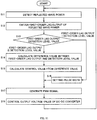
- FIG. 1 is a diagram showing the general configuration of the RF power supplying device of the present invention.
- an RF power supplying device 1 includes an RF generator unit 10 that converts the DC voltage of a DC power supply via a DC/DC converter 12, converts/amplifies DC to AC via an RF amplifier unit , and supplies the converted and amplified RF power to a load 103 such as a plasma load.
- the RF generator unit 10 includes a forward wave power control loop system 20 that performs feedback control based on the forward wave power feedback value PF detected by an RF sensor 16 at the output end and a reflected wave power control loop system 100 (30, 40, 50) that performs feedback control based on the reflected wave power feedback value PR detected by the RF sensor 16 at the output end.
- the reflected wave power control loop system 100 includes the reflected wave power peak value dropping loop system 30, arc blocking system 40, and reflected wave power amount dropping loop system 50.
- the reflected wave power peak value dropping loop system 30 performs control to drop (reduce) the peak value of reflected wave power
- the arc blocking system 40 performs control to block an arc in the plasma load
- the reflected wave power amount dropping loop system 50 performs control to drop (reduce) the power amount of reflected wave power.
- the reflected wave power peak value dropping loop system 30 and the arc blocking system 40 of the reflected wave power control loop system 100 perform control based on the signal of a peak value obtained by removing a sharp variation from the detected reflected wave power feedback value PR via a sharp variation removing unit 31.
- the reflected wave power amount dropping loop system 50 of the reflected wave power control loop system 100 performs control based on the smoothed power amount calculated by smoothing the detected reflected wave power feedback value PR via a power smoothing unit 51.
- the sharp variation removing unit 31 removes a sharp variation, which is the peak value generated when plasma rises, from the reflected wave power feedback value PR to prevent the sharp variation from being determined incorrectly as a plasma abnormality.
- the output of the sharp variation removing unit 31 is used in the control performed by the reflected wave power peak value dropping loop system 30 and the arc blocking system 40.
- the sharp variation removing unit 31 may be a first-order lag circuit configured by an LPF (low pass filter).
- the power smoothing unit 51 outputs a value corresponding to the power value that is a smoothed value calculated as the average value or effective value of the reflected wave power feedback values PR.
- the reflected wave power amount dropping loop system 50 calculates the duty ratio of the pulse control signal used to control the RF amplifier unit based on the output of the power smoothing unit 51.
- the reflected wave power control method of the present invention for use in an RF power supply, which supplies RF power to a plasma load, configures a feedback system that performs feedback control by feeding back the detection value of the output of the RF generator unit that converts the DC of a DC power supply to RF AC through the switching operation.
- the detection value of forward wave power is fed back to a forward wave power control loop system and the detection value of reflected wave power is fed back to a reflected wave power control loop system 100 that includes a plurality of loop systems.
- a reflected wave power peak value dropping loop system and an arc blocking system of the reflected wave power control loop system 100 control the output voltage to drop the peak value of reflected wave power or to block an arc.
- a sharp variation removing unit removes a sharp variation, included in the detection value of reflected wave power, to prevent a peak value, generated at plasma rise time, from being determined as a plasma abnormality, thus preventing the dropping or the blocking from being performed incorrectly.
- a reflected wave power amount dropping loop system of the reflected wave power control loop system 100 smoothes the detection values of reflected wave power via a power smoothing unit and feeds back a signal, corresponding to the smoothed power amount, to drop the power amount of reflected wave power.
- the reflected wave power control loop system includes a reflected wave power peak value dropping loop system.
- the reflected wave power peak value dropping loop system has a reflected wave power peak limit value as the threshold for determining whether the reflected wave power peak value is to be dropped.
- the reflected wave power peak value dropping loop system feeds back the difference between the detection value of reflected wave power and the reflected wave power peak limit value to the forward wave power control loop system to control the pulse width of the PWM signal, which drives the DC/DC converter provided in the RF generator unit, thus controlling the output voltage.
- the reflected wave power control loop system includes an arc blocking system.
- the arc blocking system has an arc limit value as the threshold for determining whether RF power is to be output.
- the arc blocking system controls the RF gate signal of the RF amplifier unit provided in the RF generator unit based on the comparison between the detection value of reflected wave power and the arc limit value, thus controlling the blocking of the output of RF power of the RF amplifier unit.
- the detection value of reflected wave power is sent to the sharp variation removing unit, which removes a sharp variation, included in the detection value and generated at plasma rise time, and prevents an incorrect operation.
- the reflected wave power control loop system includes a reflected wave power amount dropping loop system. Based on the comparison between the smoothed value, obtained by smoothing the detection values of reflected wave power, and the reflected wave power smoothed limit value that determines whether to drop the power amount of RF power as well as the dropping amount, the reflected wave power amount dropping loop system determines the duty ratio of the pulse control signal, which determines the time ratio between the ON state and the OFF state of the RF gate signal of the RF amplifier unit provided in the RF generator unit, thereby performing the dropping control of the power amount of RF power output from the RF amplifier unit.
- the smoothed value is the average value or the effective value of the detection values of reflected wave power.
- the reflected wave power amount dropping loop system has the reflected wave power average limit value or the reflected wave power effective limit value.
- FIG. 2 is a diagram showing the outline of power control performed in the present invention.
- the reflected wave power control of the RF power supply of the present invention uses the RF sensor 16, provided at the output end of the RF generator unit 10, to detect reflected wave power sent from the load side to the RF generator side (S1).
- a sharp variation is removed from the detection value of the detected reflected wave power (S2) and, based on the peak value of the obtained reflected wave power, the reflected wave power peak value dropping control (S3) and the arc blocking control (S4) are performed.
- a sharp variation can be removed by causing a first-order delay in the detection value of reflected wave power.
- the reflected wave power peak value dropping control uses the PWM control signal, which is based on the peak value of reflected wave power, to drive the DC/DC converter 12 of the RF generator unit 10 for controlling the output voltage.
- the arc blocking control determines if plasma is ignited based on the peak value of reflected wave power and, when a high reflected wave power is generated due to an ignition failure (S7), stops the RF gate signal and stops the output from the RF amplifier unit to stop the forward wave power (S8). After stopping the forward wave power, the arc blocking control performs the re-ignition operation to perform the plasma ignition operation repeatedly (S9).
- the re-ignition operation can be performed by the ignition retry function, which tries to ignite plasma, after a predetermined stop time elapses after the ignition is determined to fail.
- This retry function allows the user to specify the number of retries to repeat the ignition operation and the time width of the stop time. It is also possible to set up the retry function so that the retry operation is stopped if plasma cannot be ignited within the specified number of retries or to resume the retry operation after stopping the operation for a specified time.
- the smoothed value of the detection values of reflected wave power can be calculated as the average value or the effective value (S5).
- the reflected wave power amount dropping control is performed based on the calculated smoothed value.
- the reflected wave power amount dropping control sets the duty ratio of the pulse control signal based on the smoothed value of reflected wave power and performs dropping control for the RF amplifier unit based on this duty ratio (S6).
- the reflected wave power peak value dropping control (S3), arc blocking control (S4), and reflected wave power amount dropping control (S6) each of which has an individual threshold for starting the control, can perform the control operation independently of each other.
- the forward wave power control of the RF power supply of the present invention uses the RF sensor 16 to detect forward wave power sent from the RF generator side to the load side (S101).
- the forward wave power control uses the PWM control signal, which is based on the detected amount of forward wave power, to drive the DC/DC converter 12 of the RF generator unit 10 for controlling the output voltage (S102).
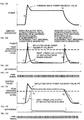
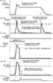
- FIG. 3 is a diagram showing the relation among the reflected wave power feedback, limit values, and arc blocking level.
- FIG. 3A shows the forward wave power feedback value PF.
- the first-order lag output of reflected wave power 202 indicates the output obtained by causing a first-order lag in the reflected wave power feedback value PR
- the smoothed value 203 indicates the average value or effective value of the reflected wave power feedback values PR.
- FIG. 3B also shows the limit values (reflected wave power smoothed limit value 301, reflected wave power peak limit value 302) and the arc limit value 303 that is the arc blocking level.
- a forward wave power feedback value 200 and a reflected wave power feedback value 201 are each indicated by an envelope curve in FIG. 3
- the output of the RF sensor 16 may be not only a DC voltage output but also an RF AC voltage output.
- the first-order lag output of reflected wave power 202 may be obtained by causing a first-order lag in the reflected wave power feedback value PR to produce a signal from which a sharp variation, which occurs sharply at plasma rise time, is reduced.
- This first-order lag output of reflected wave power 202 is compared with the reflected wave power peak limit value 302. As a result, if the first-order lag output of reflected wave power 202 reaches the reflected wave power peak limit value 302, the reflected wave power peak value dropping control is performed to reduce the peak value of reflected wave power.
- the ignition of plasma is determined to fail and the arc blocking control is performed.
- the arc blocking control stops power to be supplied to the plasma load to block an arc at the plasma load.
- the smoothed value (average value or effective value) 203 reaches the reflected wave power smoothed limit value (reflected wave power average limit value or reflected wave power effective limit value) 301, the reflected wave power amount dropping operation is performed to limit the output power amount without reducing the amplitude of the output voltage of the RF generator unit. Limiting the output power in this manner reduces a heat loss in the RF power amplifier device.
- the forward wave power feedback value and the reflected wave power feedback value in FIG. 3 which are schematic examples shown for the sake of description, do not show actual examples. Nor do the limit value and the arc blocking level show actual examples.
- the present invention realizes total reflected wave power tolerance, which is the ability to tolerate total reflected wave power generated when forward wave power all returns to the generator side as reflected wave power, in the non-ignition state before plasma is ignited.
- the present invention prevents an incorrect determination caused by the peak of reflected wave power at plasma rise time and, at the same time, performs power control based on a variation in reflected wave power caused by a longer-period variation in the plasma state of the plasma load.
- This power control prevents an RF power amplifier device from being damaged by all reflected wave power and, at the same time, continues the supply of RF power without shutdown to ignite a plasma and maintains the plasma state.
- Embodiments of the present invention are described below in detail with reference to the drawings.
- the following describes an RF power supplying device and a reflected wave power control method of present invention.
- An example of the configuration of the RF power supplying device is described with reference to FIG. 4
- an example of the operation of an RF amplifier unit is described with reference to FIGS. 5 and 6
- a part of the circuit configuration of the RF power supplying device is described with reference to FIGS. 7 and 8 .
- the operation of a forward wave power control loop system of the RF power supplying device is described with reference to FIG. 9
- the operation of a reflected wave power peak value dropping loop system of the RF power supplying device is described with reference to FIG. 10 to FIG.
- an RF power supplying device 1 of the present invention includes an RF generator unit 10 that supplies RF power to a load 103, and a generator output end 101 of the RF generator unit 10 and the load 103 are connected via a coaxial cable 102.
- the coaxial cable 102 is exemplary only and is not always required in this configuration; instead of the coaxial cable 102, power may be transmitted via any other transmission line.
- Feedback control of the RF generator unit 10 is performed by the feedback systems including a forward wave power control loop system 20, a reflected wave power amount dropping loop system 50, a reflected wave power peak value dropping loop system 30, and an arc blocking system 40.
- the RF generator unit 10 includes a DC power supply 11, a DC/DC converter 12, RF amplifier units 13, a synthesizer 14, and a low-pass filter 15, with an RF sensor 16 between the low-pass filter 15 and the generator output end 101.
- the DC power supply 11 is the input supply source of the DC/DC converter 12. Instead of the DC power supply 11, a DC voltage generated by rectifying and smoothing AC voltage may also be used.
- the DC/DC converter 12 is a device that converts the voltage Edc of the DC power supply 11 to a variable DC voltage Vdc, and the converter may be configured by an inverter circuit or by a chopper circuit.
- the DC/DC converter 12 changes the conduction ratio of the semiconductor device according to the pulse width of the PWM signal, supplied from a drive circuit 25 of the forward wave power control loop system 20 and, thereby, makes variable the DC voltage Vdc of the output.
- the DC voltage Vdc of the output of the DC/DC converter 12 is sent to the RF amplifier unit 13.
- the RF amplifier unit 13 a device that converts a DC voltage to an AC voltage, may be configured by a class-D RF amplifier circuit.
- the class-D RF amplifier circuit is an RF amplifier circuit that converts the DC of the DC power supply to an RF AC through the switching operation. This amplifier circuit causes the switching device in the output stage to perform ON/OFF operation based on the RF gate signal to increase and decrease the output current between 0 and the maximum value for performing the amplification operation via DC/ACconversion.
- a class-D RF amplifier circuit with a small heat loss because of a small on-time resistance of the switching device, performs conversion efficiently.
- the RF amplifier unit 13 implemented by a class-D amplifier circuit, may be in a full-bridge inverter configuration. This amplifier unit converts the DC voltage Vdc, received from the DC/DC converter 12, to an AC RF output power. The voltage amplitude of the RF output power of the RF amplifier unit 13 is proportional to the received DC voltage Vdc. The DC to AC amplification/conversion of the RF amplifier unit 13 is performed in synchronization with the RF gate signal supplied from a gate signal generator 18.
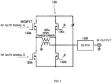
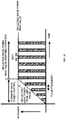
- FIG. 5 is a diagram showing an example of one configuration of the RF amplifier unit included in the RF generator.
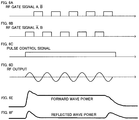
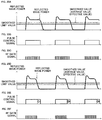
- FIG. 6 is a diagram showing the RF gate signal that drives and controls the RF amplifier unit, the RF output, and forward wave power and reflected wave power detected at the plasma load.
- MOSFETs 120a-120d are in the bridge configuration, the connection point between series-connected MOSFET 120a and MOSFET 120d and the connection point between series-connected MOSFET 120c and MOSFET 120d are connected via a main transformer 120e, and the output of the main transformer 120e, obtained via a filter 120f, is the RF output.
- the MOSFETs 120a-120d are driven and controlled by the RF gate signals A, A*, B, and B* ( FIG. 5A, FIG. 5A ).
- the RF gate signals A and A* (in FIG. 5 , the symbol “-" is shown above the letter A to indicate an inverse signal), which are signals for driving and controlling the series circuit of the MOSFET 120a and the MOSFET 120b, are in reverse phase.
- the RF gate signals B and B* (in FIG. 5 , the symbol "-" is shown above the letter B to indicate an inverse signal), which are signals for driving and controlling the series circuit of the MOSFET 120c and the MOSFET 120d, are in inverse phase.
- the RF gate signal A and the RF gate signal B are in inverse phase.
- the RF gate signals A, A*, B, and B* ( FIGS. 6A, 6B ) are controlled by the pulse control signal ( FIG. 6C ).
- the RF gate signals A, A*, B, and B* are output when the pulse control signal is on. During this period, the RF output ( FIG. 6D ) is output.
- FIGS. 6E and 6F show the forward wave power and the reflected wave power received at the plasma load.
- the reflected wave power is generated transiently at the plasma load, on which the impedance matching box is installed, when the RF gate signal ( FIGS. 6A, 6B ) rises, and is attenuated after the stabilization time elapses ( FIG. 6F ).
- the parallel connection of a plurality of RF amplifier units gives larger RF output power.
- the AC powers at the generator output end 101 of the RF generator unit 10 are placed in phase with each other by phase-synchronizing the amplification/conversion of the RF generator units.
- the synthesizer 14 is a device that combines the RF output powers, output from the plurality of RF amplifier units 13, into one.
- the synthesizer 14 may be omitted when one RF amplifier unit 13 is used.
- the RF output power, output from the RF amplifier unit 13, and the RF output power, combined into one and output by the synthesizer 14, include many higher harmonic components.
- the low-pass filter 15 shapes the waveform of the RF output power, removes the higher harmonic components included in RF power, and sends RF output power, which includes fewer higher harmonic components, to the RF sensor 16.
- the RF sensor 16 separately detects two powers, forward wave power and reflected wave power, included in the RF output power, and outputs them as a forward wave power feedback value PF and a reflected wave power feedback value PR.
- the RF output power, which passed through the RF sensor 16, is sent to the generator output end 101.
- the generator output end 101 connects the coaxial cable 102 and the RF generator unit 10. The generation of unwanted reflected wave power is prevented by matching the characteristic impedance of the generator output end 101 with the characteristic impedance of the coaxial cable 102.
- the coaxial cable 102 supplies the RF output power, received from the generator output end 101, to the load 103.
- the load 103 can match the impedance, viewed from the RF generator side, with the characteristic impedance of the generator output end 101 and the characteristic impedance of the coaxial cable 102 via the matching box (impedance matching box).
- the characteristic impedance and the matching impedance are, for example, 50 [ohm].
- the forward wave power control loop system 20 is a feedback system that feeds back the forward wave power feedback value PF, detected by the RF sensor 16, to the DC/DC converter 12 so that the forward wave power of the RF generator unit 10 becomes equal to the forward wave power instruction value.
- the forward wave power control loop system 20 includes a hold circuit 22, a forward wave power error amplifier device 23, a PWM signal generation circuit 24, and the drive circuit 25 that are connected in series in the direction from the RF sensor 16 to the DC/DC converter 12.
- a forward wave power instruction value 21 is a reference value, used during the forward wave power control, to control the magnitude of the forward wave power feedback value PF detected by the RF sensor 16.
- the PWM signal is generated that has a pulse width that makes the peak value of the forward wave power feedback value PF equal to the forward wave power instruction value 21. This PWM signal is used to pulse-control the DC/DC converter 12.
- the forward wave power feedback value PF which is output by the RF sensor 16, includes the value of the Ton area and the value of the Toff area.
- the value of the Ton area represents the magnitude of the forward wave power.
- the value of the Toff area does not represents the magnitude of the forward wave power.
- the hold circuit 22 holds only the value of the Ton area of the forward wave power feedback value PF, not including the value of the Toff area, to obtain the magnitude of the forward wave power.
- the hold circuit 22 turns on the switch according to the Ton area of the forward wave power feedback value PF, and turns off the switch and disconnects it according to the Toff area, to maintain the immediately preceding state, and holds the amplitude of the forward wave power feedback value.
- the hold circuit 22 sends the amplitude of the forward wave power feedback value PF, which is held, to the forward wave power error amplifier device 23.
- FIG. 7 is a circuit diagram showing an example of the configuration of the hold circuit 22.
- a hold circuit 61 configured by a switch circuit 65, receives the forward wave power instruction value 21 and the forward wave power feedback value PF with a resistor 63 and a resistor 64 connected to the input end of the switch circuit 65.
- the switch circuit 65 which performs switching in synchronization with ON/OFF of the forward wave power feedback value PF, sends the forward wave power feedback value PF of the Ton area, as well as the forward wave power instruction value, to an error amplifier circuit 62 connected to the output end of the switch circuit 65.
- the error amplifier circuit 62 configured by an operational amplifier 66, amplifies the difference between the forward wave power feedback value PF and the forward wave power instruction value.
- the figure shows an example in which the error amplification function is configured by hardware of the error amplifier circuit 62 that includes the operational amplifier 66.
- the function may be implemented not only by a hardware configuration but also by a software configuration in which the CPU runs a program to perform error amplification operation processing.
- a hold circuit 71 configured by a switch circuit 75 and a capacitor, receives the forward wave power feedback value PF via the input end of the switch circuit 75.
- the switch circuit 75 performs switching in synchronization with ON/OFF of the forward wave power feedback value PF and holds the forward wave power feedback value PF of the Ton area in the capacitor.
- the voltage value held in the capacitor which is the forward wave power feedback value PF
- the error amplifier circuit 72 receives the forward wave power instruction value 21 via a resistor 73.
- An error amplifier circuit 72 configured by an operational amplifier 76, amplifies the difference between the forward wave power feedback value PF and the forward wave power instruction value.
- the forward wave power error amplifier device 23 amplifies the error between the forward wave power instruction value and the forward wave power feedback value PF with a predefined gain and outputs the resulting value as the control amount.
- the PWM signal generation circuit 24 generates the PWM signal according to the larger by comparison of the two control amounts of the forward wave power error amplifier device 23 or the reflected wave power peak value power error amplifier 34.
- the control amount output by the reflected wave power peak value power error amplifier 34 is the control amount by which reflected wave power peak value dropping control is performed. If the control value of the forward wave power error amplifier device 23 is larger than the control amount of the reflected wave power peak value power error amplifier 34, forward wave power control is performed according to the control amount of the forward wave power error amplifier device 23. Conversely, if the control amount of the reflected wave power peak value power error amplifier 34 is larger than the control amount of the forward wave power error amplifier device 23, reflected wave power peak value dropping control is performed according to the control amount of the reflected wave power peak value power error amplifier 34 to drop and reduce an excessive peak value of the reflected wave power.
- the drive circuit 25 generates the drive signal, which amplifies power high enough for the semiconductor device in the DC/DC converter 12 to be driven, based on the PWM signal generated by the PWM signal generation circuit 24. Then, the drive circuit 25 sends the generated drive signal to the gate of the semiconductor device in the DC/DC converter 12 to cause the DC/DC converter 12 to perform the switching operation for converting the DC voltage Edc of the DC power supply 11 to the output voltage Vdc.
- the drive circuit 25 insulates between the reference potentials of the PWM signal generation circuit 24 and the reference potential of the DC/DC converter 12 and, if the potential of the PWM signal and the potential of the DC/DC converter 12 differ, prevents damage to, or a malfunction of, the PWM signal generation circuit 24 caused by a current from the DC/DC converter 12 to the PWM signal generation circuit 24.
- the reflected wave power peak value dropping loop system 30 is a feedback system that drops the peak value of reflected wave power of the RF generator unit 10 by feeding back the reflected wave power feedback value PR, detected by the RF sensor 16, to the DC/DC converter 12 via the forward wave power control loop system 20.
- the reflected wave power peak value dropping loop system 30 includes a sharp variation removing unit 31, a reflected wave power peak limit value 32, a hold circuit 33, and the reflected wave power peak value power error amplifier 34.
- the reflected wave power peak value dropping loop system 30 sends the output of the reflected wave power peak value power error amplifier 34 to the PWM signal generation circuit 24 of the forward wave power control loop system 20 for controlling the pulse width of the PWM signal that drives the DC/DC converter 12, thus dropping and reducing the peak value of the reflected wave power.
- the sharp variation removing unit 31 is a circuit that removes a sharp variation generated at plasma rise time.
- peak-like reflected wave power is generated inevitably at plasma rise time even when plasma is ignited successfully. If the reflected wave power generated at plasma rise time reaches the setting value (reflected wave power peak limit value), this rise in the reflected wave power is sometimes determined mistakenly as a rise in reflected wave power caused due to an abnormality in the plasma load. The dropping control of the reflected wave power peak, if performed based on this incorrect determination, could generate a problem that the ignited plasma will become unstable.
- the sharp variation removing unit 31 removes a sharp variation included in the detected reflected wave power feedback value PR and prevents incorrect determination that may be caused due to reflected wave power generated at plasma rise time.
- the sharp variation removing unit 31 may be configured by a first-order lag circuit composed of a resistor and a capacitor.
- FIG. 8 is a diagram showing an example of the configuration of the sharp variation removing unit 31.
- FIG. 8A shows an example of the circuit in which the sharp variation removing unit 31 is configured by a first-order lag circuit 80.
- This circuit may be configured by a low pass filter (LPF) composed of a resistor 81 and a capacitor 82.
- LPF low pass filter
- FIG. 8B shows another example of the configuration of the sharp variation removing unit 31.
- the sharp variation removing unit 31 may be configured by a filter circuit 90 that removes RF components.
- a switching circuit 95 switches the output of the detection signal of reflected wave power and outputs only the signal from which a sharp variation, included in the detection signal, is removed.
- a sharp variation is detected by a differentiation circuit 91, a comparator circuit 92, and a limit value 93.
- a variation in the detection signal is detected by the differentiation circuit 91, and the detected differentiation value and the limit value 93 are compared to detect a sharp variation.
- the switching circuit 95 places a sharp variation in the OFF state based on the output of the comparator circuit 92 and stops the output of the detection signal; on the other hand, the switching circuit 95 places a signal, which does not include a sharp variation, in the ON state and outputs the detection signal.
- a delay circuit 94 delays the detection signal for the time, required for the processing of the differentiation circuit 91 and the comparator circuit 92, to adjust the time of switching performed by the switching circuit 95.
- the reflected wave power peak limit value 32 is a reference value with which the output of the sharp variation removing unit 31 is compared when the reflected wave power peak value dropping operation is performed. This value is a pre-set value. During the reflected wave power peak value dropping operation, the peak value of the reflected wave power feedback is limited to a value equal to or smaller than the reflected wave power peak limit value 32.
- the hold circuit 33 may have a configuration similar to that of the hold circuit 22 provided in the forward wave power control loop system 20.
- the hold circuit 33 turns on the switch according to the Ton area of the reflected wave power feedback value PR, and turns off and disconnects the switch according to the Toff area, to maintain the immediately preceding state and holds the amplitude of the reflected wave power feedback value.
- the hold circuit 33 sends the amplitude of the reflected wave power feedback value PR, which is held, to the reflected wave power peak value power error amplifier 34.
- the reflected wave power peak value power error amplifier 34 amplifies the difference between the reflected wave power peak limit value 32 and the output of the sharp variation removing unit 31 with a pre-set gain and outputs the resulting value as the control amount.
- the control amount output by the reflected wave power peak value power error amplifier 34 is the control amount by which the reflected wave power peak value dropping control is performed.
- the PWM signal generation circuit 24 receives the output of the reflected wave power peak value power error amplifier 34 and the output of the forward wave power error amplifier device 23. If the control amount of the reflected wave power peak value power error amplifier 34 is larger than the control amount of the forward wave power error amplifier device 23, reflected wave power peak value dropping control is performed according to the control amount of the reflected wave power peak value power error amplifier 34 to drop an excessive peak value of the reflected wave power.
- the arc blocking system 40 is a feedback system that feeds back the reflected wave power feedback value PR, detected by the RF sensor 16, to the RF amplifier unit 13 to control the blocking of an arc by stopping power supplied to the plasma load.
- the arc blocking system 40 includes the sharp variation removing unit 31, provided in the reflected wave power peak value dropping loop system 30, as well as an arc limit value 41, a comparator 42, and a gate turn-off signal generator 43, and sends the output of the gate turn-off signal generator 43 to the gate signal generator 18.
- the arc blocking system 40 controls the duty ratio of the pulse control signal, which controls ON/OFF of the RF gate signal that drives the RF amplifier unit 13, in order to block an arc.
- the sharp variation removing unit 31 provided in the reflected wave power peak value dropping loop system 30 is used also in the arc blocking system 40
- other configurations are also possible.
- the sharp variation removing unit 31 may be provided separately in the arc blocking system 40.
- the sharp variation removing unit is provided independently of the reflected wave power peak value dropping loop system 30 and the arc blocking system 40; in this case, the detection value of the reflected wave power, from which a sharp variation is removed, is sent to both feedback systems, that is, to the reflected wave power peak value dropping loop system 30 and the arc blocking system 40.
- the arc limit value 41 is a level value used to determine whether plasma load ignition succeeded or failed. Whether plasma load ignition succeeded or failed is determined by determining whether the detection value, generated by removing a sharp variation from the reflected wave power feedback value PR, has reached the arc limit value 41. The reflectedwave power feedback value PR increases when the plasma load ignition failed. Therefore, if the output of the sharp variation removing unit 31 has reached the arc limit value 41, it is detected that plasma load ignition failed.
- the comparator 42 is a comparator that compares the arc limit value 41 and the output of the sharp variation removing unit 31 to determine the ignition state of the plasma load. The comparator 42 determines that the ignition succeeded if the output of the sharp variation removing unit 31 is equal to or smaller than the arc limit value 41; conversely, the comparator 42 determines that the ignition failed if the output of the sharp variation removing unit 31 exceeds the arc limit value 41.
- the gate turn-off signal generator 43 sends the gate turn-off signal to the gate signal generator 18 according to the ignition determination signal output by the comparator 42.
- the gate turn-off signal generator 43 does not send the gate turn-off signal but permits the gate signal generator 18 to output the RF gate signal.
- the gate turn-off signal generator 43 sends the gate turn-off signal to inhibit the gate signal generator 18 from outputting the RF gate signal.
- the gate signal generator 18 is a circuit that supplies the RF gate signal that controls RF gate power required to drive the RF power amplifier device in the RF amplifier unit 13.
- the gate signal generator 18 applies the generated RF gate signal to the bridge-configured MOSFETs 120 in the RF amplifier unit 13 shown in FIG. 5 to alternately switch the MOSFETs 120 between on and off for generating an RF output.
- the pulse control signal is the control signal used to control the output of the RF gate signal.
- the pulse control signal When in the ON state, the pulse control signal causes the gate signal generator 18 to output the RF gate signal and, when in the OFF state, causes the gate signal generator 18 to stop the RF gate signal.
- the RF amplifier unit 13 is driven with a duty ratio, equal to the duty ratio of the pulse control signal that is pre-set in the gate signal generator 18, to output RF power.
- the gate signal generator 18 stops the output of the pulse control signal or reduces the duty ratio to reduce RF power, output by the RF amplifier unit 13, or stops RF power.
- a brancher 17 is a circuit that branches and supplies the pulse control signal, output by the gate signal generator 18, to each of the RF amplifier units when there is a plurality of RF amplifier units 13. When there is only one RF amplifier unit, the brancher 17 is not required.
- the reflected wave power amount dropping loop system 50 is a feedback system that feeds back the reflected wave power feedback value PR, detected by the RF sensor 16, to the RF amplifier unit 13 to drop the power amount of the reflected wave power of the RF generator unit 10.
- the reflected wave power amount dropping loop system 50 includes a power smoothing unit 51 that is a smoothing unit for smoothing the power of the reflected wave power feedback value, a reflected wave power smoothed limit value 52 that is used as the threshold of the smoothed reflected wave power smoothed value, a reflected wave power smoothed value power error amplifier device 53 that amplifies power based on the difference between the reflected wave power smoothed value and the reflected wave power smoothed limit value, and a duty ratio dropping signal generator 54 that determines the duty ratio of the pulse control signal based on the output of the reflected wave power smoothed value power error amplifier device 53.
- the reflected wave power amount dropping loop system 50 sends the output of the duty ratio dropping signal generator 54 to the gate signal generator 18.
- the reflected wave power amount dropping loop system 50 includes the power smoothing unit 51, which calculates the average value or the effective value, as means for smoothing the reflected wave power feedback value PR.
- the reflected wave power amount dropping loop system 50 feeds back the calculated control amount to the RF amplifier unit 13 to control the power amount.
- the reflected wave power amount dropping loop system 50 performs the reflected wave power dropping operation to make the reflected wave power smoothed value equal to or smaller than the reference value.
- the dropping operation performed based on the average value of reflected wave power is referred to as the reflected wave power average value dropping operation
- the dropping operation performed based on the effective value of reflected wave power is referred to as the reflected wave power effective value dropping operation.
- the power smoothing unit 51 which is a circuit that smoothes the reflected wave power feedback value PR for outputting a reflected wave power smoothed value, includes an average value circuit or an effective value circuit.
- the average value circuit and the effective value circuit are each a circuit that calculates the average value or the effective value of the reflected wave power feedback values PR generated during the pulse operation of the RF generator unit 10.
- This circuit may be configured not only by a hardware circuit but also as software operation processing.
- the average value circuit when configured by hardware, may be configured by a first-order lag circuit composed of a resistor and a capacitor.
- a reflected wave power smoothed value is calculated by smoothing the reflected wave power feedback values PR as described above. This reduces heat loss in, and prevents damage to, the RF power amplifier device, not by reducing the amplitude of RF output power, but by reducing the duty ratio of the pulse control signal.
- the reflected wave power smoothed limit value (reflected wave power average limit value, reflected wave power effective limit value) is the reference value to be compared with the output of the power smoothing unit (average value circuit, effective value circuit) 51 when the reflected wave power smoothed value dropping operation (reflected wave power average value dropping operation, reflected wave power effective value dropping operation) is performed.
- the smoothed value (average value, effective value) of the reflected wave power feedback values PR becomes equal to or smaller than the reflected wave power smoothed limit value (reflected wave power average limit value, reflected wave power effective limit value) during the reflected wave power smoothed value dropping operation (reflected wave power average value dropping operation, reflected wave power effective value dropping operation), the duty ratio of the pulse control signal is adjusted, the ON state of the RF gate signal generated by the gate signal generator 18 is limited, and the power amount of reflected wave power is dropped (reduced).
- the reflected wave power smoothed value power error amplifier (reflected wave power average value power error amplifier device, reflected wave power effective value power error amplifier device) 53 amplifies the error, which is the difference between the reflected wave power smoothed limit value (reflected wave power average limit value, reflected wave power effective limit value) 52 and the output of the power smoothing unit (average value circuit, effective value circuit) 51, with a predefined gain and outputs the result as the control amount.
- the duty ratio dropping signal generator 54 is a circuit that determines the duty ratio between the ON state and the OFF state at pulse operation time according to the control amount output by the reflected wave power smoothed value power error amplifier device (reflected wave power average value power error amplifier device, reflected wave power effective value power error amplifier device) 53.
- the gate signal generator 18 receives the pulse control signal from the duty ratio dropping signal generator 54 and generates the RF gate signal whose ON state and OFF state are based on the duty ratio of the pulse control signal.
- the gate signal generator 18 also receives the gate turn-off signal from the gate turn-off signal generator 43 of the arc blocking system 40. This gate turn-off signal has priority over the duty ratio signal and stops the RF gate signal.
- the duty ratio dropping signal generator 54 When the operation does not move to the reflected wave power average value dropping operation but the usual forward wave power control is performed, the duty ratio dropping signal generator 54 does not generate the duty ratio dropping signal but generates the gate signal with the pulse control signal, which has a pre-set fixed duty ratio, and performs the pulse operation.
- the forward wave power control is performed by the forward wave power control loop system 20 shown in FIG. 9 (indicated by bold arrows).
- the output Vdc of the DC/DC converter 12 is made variable to control the amplitude of the RF output power so that the forward wave power instruction value 21 always matches the peak value of the forward wave power feedback value PF.
- the control loop moves from the forward wave power control loop system 20 to a reflected wave power control loop system 100 (reflected wave power peak value dropping loop system 30, arc blocking system 40, or reflected wave power amount dropping loop system 50) in which the dropping operation or the blocking operation is performed.
- a reflected wave power control loop system 100 reflected wave power peak value dropping loop system 30, arc blocking system 40, or reflected wave power amount dropping loop system 50
- FIG. 10 shows the reflected wave power peak value dropping control loop system.
- reflected wave power is generated. If the output (for example, first-order lag output) obtained by removing a sharp variation in reflected wave power from the reflected wave power feedback value PR, which is obtained by detecting the reflected wave power, exceeds the reflected wave power peak limit value 32, the reflected wave power peak value dropping loop system 30 shown in FIG. 10 (indicated by bold arrows) performs the reflected wave power peak value dropping operation.
- the output for example, first-order lag output
- the amplitude of the RF output power is limited to a predetermined value or lower.
- This reflected wave power peak value dropping operation protects the RF power amplifier device from an overload or a surge voltage when reflected wave power is generated, and prevents the RF power amplifier device from being destroyed.
- the RF sensor 16 detects reflected wave power (S11) and sends the detected reflected wave power to the sharp variation removing unit 31 to obtain the output (for example, first-order lag output) from which a sharp variation is removed (S12). If the output (for example, first-order lag output), from which a sharp variation in the reflected wave power is removed, exceeds the reflected wave power peak limit value 32 that is the detection level of the reflected wave power peak value (S13), the difference between the output (for example, first-order lag output), from which a sharp variation in the reflected wave power is removed, and the reflected wave power peak limit value 32 is calculated (S14) and, based on this difference, the control value is calculated (S15). Based on the control value, the PWM signal generation circuit 24 generates the PWM signal (S17). The difference and the control value can be generated by the reflected wave power peak value power error amplifier 34.
- the PWM signal generation circuit 24 generates the PWM signal (S17) based on the predetermined setting pulse width (S16).
- the DC/DC converter 12 is driven by the generated PWM signal to control the output voltage value (S18).
- FIG. 12 is a diagram showing the forward wave power control and the reflected wave power peak value dropping operation.
- the horizontal axis of FIG. 12 indicates the time, and the vertical axis indicates the reflected wave power.
- the DC/DC converter is driven by the PWM signal with the predetermined pulse width. This driving increases forward wave power (not shown) and, at the same time, increases reflected wave power.
- the reflected wave power peak value dropping operation is started.
- the reflected wave power peak value dropping operation decreases the pulse width of the PWM signal so that the peak value of reflected wave power does not exceed the reflected wave power peak limit value.
- FIG. 13 schematically shows the reflected wave power peak value dropping operation when plasma ignition succeeded and when plasma ignition failed.
- the waveforms shown in FIG. 13 are not actual waveforms but are simplified for the sake of description.
- FIG. 13A shows the forward wave power feedback value.
- the bold solid line indicates the reflected wave power feedback value PR
- the light solid line indicates the first-order lag output of the reflected wave power feedback value
- the chain line indicates the peak dropping detection level.
- FIGS. 13A to 13D show the waveform when the ignition succeeded
- FIGS. 13E to 13G show the waveform when the ignition failed.
- the reflected wave power increases at the plasma rise time T1 and at the plasma fall time T2.
- the reflected wave power peak value dropping operation is performed based on the reflected wave power feedback value PR (indicated by bold solid line)
- PR indicated by bold solid line
- the output generated by removing a sharp variation from the reflected wave power feedback value (for example, first-order lag output) (indicated by light solid line) does not reach the peak dropping detection level and, therefore, the reflected wave power peak value dropping operation is not performed.
- the PWM signal is not changed ( FIG. 13D ) and the forward wave power control is maintained.
- the output generated by removing a sharp variation from the reflected wave power feedback value (for example, first-order lag output) (indicated by light solid line) reaches the peak dropping detection level at the time T3, which is after the time T1, at ignition failure time and the reflected wave power peak value dropping operation is started.
- the pulse width of the PWM signal is generated ( FIG. 13G ) based on the difference ( FIG. 13F ) between the first-order lag output of the reflected wave power and the peak dropping detection level, and the reflected wave power voltage peak is dropped.
- the reflected wave power peak value dropping operation is terminated and the operation returns from the reflected wave power peak value dropping control to the forward wave power control.
- FIG. 14 shows the arc blocking control loop system.
- the arc blocking system 40 shown in FIG. 14 (indicated by bold arrows in FIG. 14 ) performs the arc blocking operation.
- the gate turn-off signal generator 43 sends the blocking signal to stop the operation of the RF amplifier unit 13 for blocking an arc.
- the pulse width of the RF output power during the arc blocking operation becomes much shorter than the pre-set pulse width used in the duty ratio during the normal pulse operation and, therefore, the RF power amplifier device is not destroyed.
- the RF sensor 16 detects reflected wave power (S21) and sends the detected reflected wave power to the sharp variation removing unit 31 to remove a sharp variation.
- S21 reflected wave power
- the sharp variation removing unit 31 outputs a first-order lag.
- a sharp variation is removed by generating a first-order lag output of reflected wave power (S22). If the obtained first-order lag output exceeds the arc limit value 41 that is the arc blocking detection level (S23), the gate turn-off signal is generated (S24).
- the gate signal generator 18 stops the output of the RF gate signal (S25) to stop the output of the RF amplifier unit (S26).
- the gate signal generator 18 generates the RF gate signal based on the predetermined duty ratio of the pulse control signal to maintain the output of the RF amplifier unit or, if the output of the RF amplifier unit is stopped, to restart the output (S27).
- the ignition retry function may be used to perform the re-ignition operation.
- the re-ignition operation tries the ignition after a predetermined stop time elapses from the time the ignition is determined to fail.
- This retry function allows the operator to specify the number of retries to repeat the ignition operation or the time width of the stop time. The operator may also specify that, if the ignition does not succeed within a specified number of retries, the retry operation be stopped or the retry operation be once stopped and then restarted after a predetermined time.
- FIG. 16 schematically shows the arc blocking operation when plasma ignition succeeded and when plasma ignition failed.
- the waveforms shown in FIG. 16 are not actual waveforms but are simplified for the sake of description.
- FIG. 16A and FIG. 16D show forward wave power feedback values.
- the bold solid line indicates the reflected wave power feedback value PR
- the light solid line indicates the first-order lag output of the reflected wave power feedback value
- the chain line indicates the arc limit value.
- FIGS. 16A to 16C show the waveform when the ignition succeeded
- FIGS. 16D to 16F show the waveform when the ignition failed.
- the reflected wave power increases at the plasma rise time t1 and at the plasma fall time t2 ( FIG. 16B ).
- the arc blocking operation is performed based on the reflected wave power feedback value PR (indicated by bold solid line), it is incorrectly determined that an abnormal condition, such as arc generation, is generated even when the normal ignition operation is performed, and the plasma is extinguished by the arc blocking operation.
- the output generated by removing a sharp variation from the reflected wave power feedback value does not reach the arc limit value that is the arc blocking level and, therefore, the arc blocking operation is not performed.
- the gate turn-off signal is not output ( FIG. 16C ) and the forward wave power control is maintained.
- the output generated by removing a sharp variation from the reflected wave power feedback value (first-order lag output (indicated by light solid line)) reaches the arc limit value, which is the arc blocking detection level, at the time t3, which is after the time t1, at ignition failure time ( FIG. 16E ).
- the gate turn-off signal is generated ( FIG. 16F ) and the arc blocking operation is started.
- FIG. 17 schematically shows the reflected wave power amount dropping operation.
- reflected wave power is generated. If the reflected wave power smoothed value obtained by smoothing the reflected wave power feedback value PR, obtained by detecting the reflected wave power, exceeds the reflected wave power smoothed limit value 52, the reflected wave power amount dropping loop system 50 (indicated by bold arrows) shown in FIG. 17 performs the reflected wave power amount dropping operation.
- the reflected wave power smoothed value is the average value or the effective value of reflected wave power.
- the reflected wave power dropping operation controls the duty ratio of the pulse control signal so that the output of the power smoothing unit 51 does not exceed the reflected wave power smoothed limit value 52. Limiting the width of the ON state of the RF gate signal in this manner prevents the power amount of RF output power from exceeding a predetermined value.
- the reflected wave power amount dropping operation reduces the output power without reducing the amplitude of the PF output voltage and reduces a heat loss in the RF power amplifier device, thus preventing destruction.
- the RF sensor 16 detects reflected wave power (S31) and sends the detected reflected wave power to the power smoothing unit 51 to calculate the reflected wave power smoothed value (S32). If the reflected wave power smoothed value exceeds the reflected wave power smoothed limit value 52 that is the reflectedwave power detection level (S33), the difference between the reflected wave power smoothed value and the reflected wave power smoothed limit value 52 is calculated (S34). The control value is calculated based on this difference (S35), and the duty ratio of the pulse control signal corresponding to the control value is calculated through duty ratio conversion. To perform the duty ratio conversion, the relation between the control value and the duty ratio corresponding to this control value is predetermined and, based on this correspondence, the duty ratio is calculated from this control value.
- the duty ratio dropping signal generator 54 Based on the calculated duty ratio, the duty ratio dropping signal generator 54 generates the duty ratio dropping signal.
- the gate signal generator 18 generates the RF gate signal, whose ON state is reduced, based on the duty ratio dropping signal.
- the duty ratio dropping signal is a pulse control signal that defines the duty ratio between the ON sate and the OFF state of the RF gate signal. Reducing the ON state reduces the power amount of forward wave power and, thereby, reduces the power amount of reflected wave power (S38).
- the duty ratio dropping signal generator 54 does not generate the duty ratio dropping signal.
- the gate signal generator 18 generates the pulse control signal (S38) based on the predetermined setting duty ratio (S37), generates the RF gate signal based on the pulse control signal (S39), and drives the RF amplifier unit 13 by the generated RF gate signal to control the output power (S40).
- FIG. 19 is a diagram showing the forward wave power control and the reflected wave power amount dropping operation.
- the horizontal axis of FIG. 19 indicates the time, and the vertical axis indicates the power ( FIG. 19A ) and the load voltage ( FIG. 19B ).
- the RF amplifier unit 13 is driven by the RF gate signal that has the ON state and the OFF state of the predetermined duty ratio. This driving increases the power of forward wave power (not shown) and, at the same time, increases the power amount of reflected wave power.
- the reflected wave power smoothed value average value or effective value
- the reflected wave power amount dropping operation is started.
- the reflected wave power amount dropping operation decreases the duty ratio of the pulse control signal to narrow the width of the ON state during which the RF gate signal is output. By doing so, the reflected wave power amount dropping operation controls the power amount of reflected wave power so that it does not exceed the reflected wave power smoothed limit value.
- FIG. 19A shows an example in which the average value is used as the smoothed value.
- the upper limit of the reflected wave power average value can be controlled so that it does not exceed the reflected wave power average limit value.
- FIG. 19B which shows the load voltage, indicates that the voltage applied to the load during the reflected wave power average value dropping operation is kept constant.
- the supplied power is reduced by reducing the number of cycles of RF voltages applied during one period of the pulse operation.
- FIG. 20 schematically shows the reflected wave power amount dropping operation.
- the waveforms shown in FIG. 20 are not actual waveforms but are simplified for the sake of description.
- FIG.20A to 20C show the case in which the reflected wave power smoothed value exceeds the reflected smoothed limit value
- FIG.20D to 20F show a state after the reflected wave power amount dropping operation.
- FIG. 20A shoes the reflected wave power
- FIG. 20D shows the reflected wave power smoothed value
- FIG.20D,20E show the pulse control signal
- FIG.20C,20F show a RF gate signal.
- he pulse control signal in the figures represent the ON state, in which the gate signal is output, and the OFF state in which the gate signal is not output.
- the signal waveforms are not actual waveforms but are simplified for the sake of description.
- FIG.20D to FIG.20F show a state after the reflected wave power amount dropping operation.
- the output power is controlled by that the duty ratio of the pulse control signal is reduced, and the pulse control signal ( FIG.20E ) determined by the duty ratio is output.
- the RF signal is generated based on the pulse control signal ( FIG.20F ) and the reflected wave power amount is dropped.
- Control Reflected wave power amount dropping control Reflected wave power peak value dropping control Arc blocking control Detection level Low Intermediate High Control value Smoothed value of reflected wave power (average value, effective value) Signal generated by removing sharp variation from reflected wave power (first-order lag) Signal generated by removing sharp variation from reflected wave power (first-order lag) Control target RF output power Smoothed power amount of reflected wave power RF output power Peak value of reflected wave power RF output power Peak value of reflected wave power RF output power Peak value of reflected wave power Control target unit RF power amplifier unit DC/DC converter (voltage conversion unit) RFpower amplifier unit Control amount Duty ratio between ON state and OFF state of gate signal, Pulse control signal of class-D amplifier unit PWM signal of DC/DC converter Gate signal of class-D amplifier unit Purpose • Prevention of thermal destruction of RF power amplifier device
- the RF power supplying device and the reflected wave power control method of the present invention are applicable to a power supply that supplies power to a plasma generation device.
Landscapes
- Physics & Mathematics (AREA)
- Engineering & Computer Science (AREA)
- Plasma & Fusion (AREA)
- Chemical & Material Sciences (AREA)
- Analytical Chemistry (AREA)
- Electromagnetism (AREA)
- Spectroscopy & Molecular Physics (AREA)
- Power Engineering (AREA)
- Plasma Technology (AREA)
Description
- The present invention relates to a reflected wave power control method and an RF power supplying device for controlling reflected wave power that is transmitted from a load side to an RF generator side when RF power is supplied from the RF generator to the load.
- An RF generator that converts the DC of a DC power supply to RFAC through the switching operation is known. As this RF generator, a class-D RF generator using a class-D amplifier circuit (Class D: IEC International Standard IEC 60268-3 4 classes of operation) is known.
- A class-D RF generator causes the RF power amplifier device to perform the switching operation via the RF gate signal, which has a predetermined duty ratio, to convert the DC of a DC power supply to RFAC and supplies the obtained RF AC to a load as RF forward wave power. The class-D RF generator adjusts the output through the pulse operation. The pulse operation is performed in a driving mode in which ON state and the OFF state are alternated by the RF gate signal. In the ON state, the switching operation is performed by the RF power amplifier device and RF power is output; in the OFF state, the switching operation is not performed and RF power is not output. The RF output power is adjusted by changing the duty ratio that is a time ratio between the ON state and the OFF state. The duty ratio between the ON state and the OFF state can be controlled by a duty ratio between the ON state and the OFF state of the pulse control signal. In this specification, RF means high frequency.
- When RF power is supplied from an RF power generator to a load, for example, to a load such as a plasma treatment device, the load impedance varies according to the state of a plasma discharge. When the load impedance varies, reflected wave power that returns from the load side to the RF generator side varies.
- In some cases, reflected wave power affects a class-D RF generator. For example, an RF power amplifier device, which is one of the components of a class-D RF generator, may suffer thermal damage due to heat generated by an internal loss caused by reflected wave power or may suffer insulation damage due to a surge voltage of reflected wave power. A still larger reflected wave power sometimes damages the DC power supply that is one of the components of a class-D RF generator.
- In particular, when a class-D RF generator supplies RF power to a plasma load through the pulse operation, forward wave power all returns to the generator side as reflected wave power in the non-ignition state in which plasma is not yet ignited. Therefore, a class-D RF generator is required to tolerate total reflected wave power. In the description below, reflected wave power generated when forward wave power all returns to the generator side is called total reflected wave power, and the ability to tolerate total reflected wave power during RF power supply is called total reflected wave power tolerance.
- The total reflected wave power tolerance includes the ability not only to prevent an RF power amplifier device from being damaged by total reflected wave power but also to continue the plasma ignition operation by continuously supplying power without interruption from the time the ignition operation is started to the time the supply of RF power is stopped upon determination that the ignition has failed.
- Conventionally, to realize such total reflected wave power tolerance, the present applicant has proposed a plasma generation power supply (see Patent Literature 1).
Patent Literature 1 describes a technology that uses load impedance, viewed from an RF power amplifier device, in the delay state in order to suppress accumulated carriers in the body diode of the RF power amplifier device and thereby reduces the switching loss of the circuit. To realize total reflected wave power tolerance, it is further required to limit the ignition time, necessary for the ignition operation at plasma ignition time, in advance and, by doing so, to limit the reflected wave power within this ignition time to the same power level as that of the rated power of forward wave power. - Not only a class-D RF generator, a class-C RF generator is also known as a RF generator that is usually used. For use by a usually used RF generator device such as a class-C RF generator, a technology is known that reduces forward wave power on the supplying side in order to reduce the supply of reflected wave power to a level equal to or lower than the rated output when reflected wave power is generated. In this way, the technology prevents the device on the RF generator side from being damaged (Patent Literature 2 to Patent Literature 7).
- Patent Literatures 2 and 3 disclose technologies for stopping the supply of power, and Patent Literatures 4 to 7 disclose technologies for reducing forward wave power.
- Patent literature 2 describes a shutdown method for controlling the forward wave power value of an RF plasma power supply so that the reflected wave power value becomes equal to or lower than 10% to 20% of the rated output. Patent literature 3 describes a microwave power supply system that uses a signal, output from a reflected wave power detector, to temporally integrate the differences between the magnitude of the signal, corresponding to the reflected microwave power, and the charge/discharge reference value and, if the magnitude of the integrated signal having the magnitude corresponding to the integrated value exceeds the allowable reference value, shuts down the supply of power.
- Patent literature 4 describes a technology that reduces the output power using a mixer when reflected wave power exceeds the limit value.
Patent literature 5 describes a technology that generates a power control signal using the power reduction signal, output from the reflected wave power detection signal, and forward wave power.Patent literature 6 describes a technology that calculates the difference between the reflected wave power, which is detected and fed back, and the reflected wave power that is set and, based on the calculated difference, drops the forward wave power. Patent literature 7 describes a technology that calculates a reflected wave coefficient based on the reflected wave power, corrects the magnitude of the gain of the attenuator according to the calculated reflected wave coefficient, and supplies required power to the load. -
Patent literature 8 describes a technology that differentiates the output of the sensor, which measures reflected wave power, and determines the generation of an abnormal discharge based on the degree of temporal variations in the reflected wave of RF power output by the differentiation. Patent literature 9 describes a technology that comprises a reflected wave power amount dropping loop system.Patent literature 10 describes a technology that comprises a reflected wave power peak value dropping loop system and an arc blocking system. -
- Patent Literature 1: Japanese Patent No.
3641785 - Patent Literature 2: Japanese Patent Publication No.
7-32078 - Patent Literature 3: Japanese Patent Application Publication No.
2004-71269 - Patent Literature 4: Japanese Patent Application Publication No.
10-257774 - Patent Literature 5: Japanese Patent No.
3998986 - Patent Literature 6: Japanese Patent Application Publication No.
2004-8893 - Patent Literature 7: Japanese Patent Application Publication No.
2005-136933 - Patent Literature 8: Japanese Patent No.
3893276 - Patent Literature 9:
US 2003/042977 A1 (paragraph [0035]) - Patent Literature 10:
JP 2003 143861 A - When a class-D RF generator supplies RF power to a plasma load through the pulse operation, it is required, in the non-ignition state before plasma is ignited, to supply a high load-end power to the load against total reflected wave power, generated when forward wave power all returns to the generator side as reflected wave power and, thereby, to increase plasma ignition ability during the pulse operation, with no damage to the RF power amplifier device caused by total reflected wave power at pulse operation time.
- According to the technology described in
Patent Literature 1, the load impedance is used in the delay state to reduce the switching loss of the circuit. However, when the plasma ignition time is limited to realize total reflected wave power tolerance, plasma may remain un-ignited if it takes long until plasma is ignited. - According to the technology described in Patent Literatures 2 and 3, the power supply is stopped. The technology described in Patent Literature 2 controls forward wave power so that the reflected wave power value becomes equal to or lower than 10% - 20% of the rated output. The technology described in Patent Literature 3 controls power shutdown based on the output of the charge/discharge circuit. These technologies cannot maintain the supply of RF power while tolerating total reflected wave power, meaning that total reflected wave power tolerance cannot be realized.
- Even if the RF generator and the plasma load match properly when the DC of the DC power supply is converted to RF AC via the switching operation in the RF generator and the forward wave power of RF power is supplied to the plasma load, the load impedance of the plasma load varies largely at plasma rise time. This variation in the load impedance generates reflected wave power that returns from the plasma load side to the generator side. The reflected wave power generated at plasma rise-time varies largely in a short time.
- According to the power control described in Patent Literature 4 to Patent Literature 7, the power is controlled based on the instantaneous value of reflected wave power. Therefore, when reflected wave power rises rapidly at plasma rise time and its peak value exceeds the setting value, power reduction is started by power control. When the power supplied to the plasma load is limited by power control, the supplied power is limited before plasma is ignited with the result that plasma is not ignited successfully. Even if plasma is ignited successfully, the problem is that the reduced power supply makes it difficult to maintain plasma, meaning that normal plasma generation is difficult.
- That is, the conventional power control reduces power based on an instantaneous value of reflected wave power. This may result in an incorrect determination that the peak of reflected wave power at plasma rise time is mistaken as an increase in reflected wave power caused by a plasma state change that will exist for a long time. If the power is turned off or reduced based on this incorrect determination, it becomes difficult to ignite or maintain plasma.
- Therefore, in an RF generator that supplies RF power to a plasma load through the pulse operation, it is an object of the present invention, in the non-ignition state before plasma is ignited, to solve the above-described conventional problems with total reflected wave power tolerance that is the ability to tolerate total reflected wave power generated when forward wave power all returns to the generator side as reflected wave power. More specifically, when a class-D RF generator supplies RF power to a plasma load through the pulse operation, an object of the present invention is to realize total reflected wave power tolerance that is the ability to tolerate total reflected wave power generated when forward wave power all returns to the generator side as reflected wave power in the non-ignition state before plasma is ignited, to prevent an RF power amplifier device from being damaged by all reflected wave power during the pulse operation and, at the same time, to continue the plasma ignition operation by continuously supplying power without shutting down the supply of RF power in order to increase the plasma ignition performance during the pulse operation time.
- In an RF power supply for supplying RF power to a plasma load, the present invention relates to reflected wave power control in which the reflected wave power of an RF generator is detected and, using the detected reflected wave power, the RF generator is controlled. For a short-time variation in reflected wave power, reflected wave power is controlled based on a variation in the peak value of the detection value of reflected wave power. For a long-time variation in reflected wave power, reflected wave power is controlled based on a variation in a smoothed value obtained by smoothing detection values of reflected wave power.
- According to the present invention, a reflected wave power control loop system includes a reflected wave power peak value dropping loop system and an arc blocking system that perform control based on a peak variation in reflected wave power and a reflected wave power amount dropping loop system that performs control based on a smoothed power amount of reflected wave power.
- The reflected wave power peak value dropping loop system of the present invention controls the DC voltage of the DC power supply of the RF generator unit based on the peak value of reflected wave power and, through the voltage control of the DC power supply, performs dropping control of the peak value of reflected wave power. The reflected wave power peak value dropping loop system is a control system that drops (reduces) the peak value of reflected wave power when the peak value of reflected wave power exceeds a setting value (reflected wave power peak limit value). This system drops (reduces) the amplitude of the peak value of reflected wave power to prevent the RF power amplifier device from being destroyed due to an overload or a surge voltage.
- The reflected wave power peak value dropping loop system is configured to control the DC voltage of the DC power supply of the RF generator unit. The system feeds back the peak value of reflected wave power to this DC power supply to cause it to drop the DC voltage, thus speedily dropping the peak value of reflected wave power.
- The arc blocking system of the present invention controls whether to output from the RF amplifier unit of the RF generator unit based on the peak value of reflected wave power and thereby controls whether to supply power to the plasma load to control the blocking of an arc at the plasma load. The arc blocking system is a control system that stops the power supply when the peak value of reflected wave power exceeds the setting value (arc limit value). When the ignition fails and a high reflected wave power is generated that exceeds the arc blocking level at which that an arc at the plasma load is blocked, the arc blocking system stops the power supply to extinguish an arc in the plasma load. It is also possible to configure the system in such way that, when an arc is blocked, the ignition retry function, which performs the re-ignition operation after a predetermined time, is activated to ignite plasma again.
- The reflected wave power peak value dropping loop system and the arc blocking system of the present invention perform the control to drop the peak value of reflected wave power or perform control to stop the power supply when the peak value of reflected wave power exceeds the setting value that is set in each control system.
- At least one of the reflected wave power peak value dropping loop system and the arc blocking system of the present invention includes a sharp variation removing unit that removes a sharp variation from the detection value of reflected wave power. The sharp variation removing unit removes a sharp variation amount, generated by a sharp variation, from the detection value of reflected wave power, and feeds back a signal corresponding to the peak value of reflected wave power not generated by the sharp variation and existing longer than the sharp variation. The use of the peak value, from which a sharp variation amount is removed, prevents an incorrect determination that could be generated by the feedback control based on a peak value caused by a sharp variation generated at a plasma rise time. The sharp variation removing unit may be configured by a first-order lag circuit such as a low pass filter.
- The reflected wave power amount dropping loop system of the present invention controls the amplification of the RF amplifier unit of the RF generator unit, based on the smoothed power amount of reflected wave power, to control the amount of power to be supplied to the plasma load for controlling whether to drop the smoothed power amount of reflected wave power. The reflected wave power amount dropping loop system is a control system that drops (reduces) the power amount of reflected wave power when the smoothed value, such as the average value or the effective value of the power amount of reflected wave power, exceeds the setting value (reflected wave power smoothed limit value). This system drops (reduces) the power amount of reflected wave power with the amplitude of the output voltage maintained, thus preventing thermal damage to the RF power amplifier device.
- The control systems of the present invention, including the reflected wave power peak value dropping loop system, arc blocking system, and reflected wave power amount dropping loop system, can be each controlled independently. The setting values used for the control systems are the reflected wave power peak limit value, arc limit value, and reflected wave power smoothed limit value. The largest value is the arc limit value, the next largest value is the reflected wave power peak limit value, and the smallest value is the reflected wave power smoothed limit value.
- The reflected wave power peak limit value is an index of effect on the RF amplifier device caused by an increase in the peak value of reflected wave power such as an overload or a surge voltage. When the peak value of reflected wave power exceeds this setting value, the reflected wave power peak value dropping loop system drops the peak value of reflected wave power and performs control so that the peak value of reflected wave power does not become equal to or larger than the setting value. The control based on this limit value protects the destruction of the RF power amplifier device from an overload or a surge voltage when reflected wave power is generated.
- The arc limit value, which is a threshold for detecting an increase in reflected wave power generated by a failure in the ignition of the plasma load, is set as an arc blocking level. When the peak value of reflected wave power exceeds the arc blocking level, the arc blocking system determines that the ignition has failed and starts the arc blocking operation.
- The reflected wave power smoothed limit value is a setting value used as an index of thermal effect on the RF power amplifier device caused by an increase in the power amount of reflected wave power. When the average value or the effective value of reflected wave power exceeds this setting value, the reflected wave power amount dropping loop system controls the duty ratio of the pulse control signal to control a drop (reduction) in the power amount of reflected wave power for preventing thermal damage to the RF power amplifier device. In the dropping control of the duty ratio, the reflected wave power amount dropping loop system reduces the ratio of the ON state in the time ratio between the ON state and the OFF state of the pulse control signal to reduce reflected wave power.
- The reflected wave power control system of the present invention uses the reflected wave power peak value dropping loop system, arc blocking system, and reflected wave power amount dropping loop system described above to provide total reflected wave power tolerance, which is the ability to tolerate total reflected wave power generated when forward wave power all returns to the generator side as reflected wave power, in the non-ignition state before the plasma is ignited. Total reflected wave power tolerance, provided in this manner, prevents the RF power amplifier device from being damaged by total reflected wave power and, until reflected wave power generated due to an ignition failure becomes so high that the power supply must be stopped, continues supplying power without stopping the supply of RF power for continued plasma ignition operation, thus increasing the plasma ignition performance during the pulse operation.
- One aspect of the present invention is an RF power supplying device and another aspect is a reflected wave power control method. The invention is defined by the claims.
- An RF power supplying device of the present invention, which is an RF power supplying device that supplies RF power to a plasma load, includes an RF generator unit that converts DC of a DC power supply to RF AC through a switching operation and outputs RF power; and a plurality of feedback systems that feeds back a detection value of the RF output of the RF generator unit for performing feedback control. The feedback system includes a forward wave power control loop system that feeds back a detection value of forward wave power, which is sent from the RF generator unit to a plasma load, for controlling the forward wave power; and a plurality of reflected wave power control loop systems each of which feeds back a detection value of reflected wave power, which is sent from the plasma load to the RF generator unit, for controlling the reflected wave power.
- The arc blocking system does not form a control loop but, after performing the blocking processing to stop forward wave power, performs the plasma ignition operation through the re-ignition operation. Considering that this operation forms one type of loop, the arc blocking system is included in the reflected wave power control loop system in the description below.
- In the feedback system of the reflected wave power control loop system, if a peak value generated at plasma rise time is determined incorrectly as a rise in reflected wave power caused by an abnormal condition of the plasma load, the feedback control will result in an incorrect operation.
- To reduce this incorrect operation caused by a peak value, the reflected wave power peak value dropping loop system and the arc blocking system of the present invention include a sharp variation removing unit that removes a sharp variation from the detection value of reflected wave power detected at the output end of the RF generator unit.
- The sharp variation removing unit, which may be configured by a first-order lag circuit, removes a sharp variation, included in the detection value, by causing a first-order lag in the detection value of reflected wave power. By causing a first-order lag in the detection value of reflected wave power, the first-order lag circuit can reduce a sharp variation included in reflected wave power generated at plasma rise time, prevent an incorrect determination caused by a variation that is not related to the plasma load and generated at plasma rise time, and thus prevent an incorrect operation that reduces the supply of RF power.
- The sharp variation removing unit may be configured not only as a first-order lag circuit but also as a unit that detects a time at which the detection value of reflected wave power varies sharply and removes the detection value at this time.
- The reflected wave power amount dropping loop system provided in the reflected wave power control loop system of the present invention, configured to calculate the smoothed value of reflected wave power, includes a power smoothing unit that outputs the average value or the effective value of the detection values of reflected wave power. As the criterion for determining whether the power amount of RF power is to be dropped and as the reflected wave power smoothed limit value that determines the drop amount used in the dropping control, the reflected wave power average limit value or the reflected wave power effective limit value is provided. The reflected wave power amount dropping loop system calculates the amount of error between the smoothed value, obtained by the power smoothing unit, and the reflected wave power smoothed limit value (reflected wave power average limit value or reflected wave power effective limit value) and, based on the calculated amount of error, performs the dropping control for the reflected wave power amount.
- The following describes the reflected wave power peak value dropping loop system, arc blocking system, and reflected wave power amount dropping loop system.
- The reflected wave power control loop system of the present invention includes the reflected wave power peak value dropping loop system that drops (reduces) the peak value of reflected wave power. The reflected wave power peak value dropping loop system has a reflected wave power peak limit value as the threshold for determining whether the reflected wave power peak value is to be dropped.
- The reflected wave power peak value dropping loop system of the present invention feeds back the difference between the peak value of reflected wave power and the reflected wave power peak limit value to the forward wave power control loop system as the feedback signal. Based on the feedback signal fed back from the reflected wave power peak value dropping loop system, the forward wave power control loop system controls the pulse width of the PWM signal, which drives the DC/DC converter provided in the RF generator unit, to control the output voltage.
- The detection value of reflected wave power may include a peak generated by a sharp variation at the time plasma rises. This peak is not caused by a plasma abnormality. Therefore, if the reflected wave power peak value is dropped based on this peak value when the plasma state is normal, an incorrect control operation would be performed on the assumption that a plasma abnormality has occurred.
- To avoid such an incorrect determination, the sharp variation removing unit is provided. The sharp variation removing unit outputs a signal, generated by removing a sharp variation included in the detection value of reflected wave power, as the peak value of reflected wave power. By feeding back the difference between the peak value, from which a sharp variation is removed, and the reflected wave power peak limit value to the forward wave power control loop system as the feedback signal, an incorrect operation due to a sharp variation can be avoided.
- The reflected wave power control loop system of the present invention includes an arc blocking system that prevents damage caused by excessive reflected wave power. When the ignition fails and an excessive amount of reflected wave power is generated, the arc blocking system stops the supply of power to the plasma load to block an arc in the plasma load. The arc blocking system has an arc limit value as the threshold for determining whether the output of RF power is to be stopped.
- Based on the comparison between the peak value of reflected wave power and the arc limit value, the arc blocking system of the present invention controls the pulse control signal, which generates the RF gate signal for driving the RF amplifier unit provided in the RF generator unit, to control whether to output RF power from the RF amplifier unit. The RF amplifier unit converts a DC voltage to AC RF power, for example, via a full-bridge inverter. When converting from DC to AC, the RF amplifier unit performs amplification/ conversion in synchronization with the RF gate signal that switches the switch device of the inverter. By controlling the pulse control signal that generates the RF gate signal to be sent to the RF amplifier unit, the arc blocking system can control the output of RF power.
- In the arc blocking system, too, a peak included in the detection value of reflected wave power and generated by a sharp variation at plasma arise time is sometimes determined incorrectly as a plasma abnormality. To avoid such an incorrect determination, the sharp variation removing unit may be provided. Based on the comparison between the peak value of reflected wave power, from which a sharp variation is removed by the sharp variation removing unit, and the arc limit value, the arc blocking system performs the blocking control, thus avoiding an incorrect operation that may be caused by a sharp variation.
- The reflected wave power peak value dropping loop system and the arc blocking system use the sharp variation removing unit to remove a variation from reflected wave power. This prevents a peak value, generated when plasma rises, from being determined incorrectly as a plasma abnormality.
- The reflected wave power control loop system of the present invention includes the reflected wave power amount dropping loop system that drops (reduces) the power amount of reflected wave power.
- The reflected wave power amount dropping loop system of the present invention determines the duty ratio of the pulse control signal, which determines the time ratio between the ON state and the OFF state of the RF gate signal of the RF amplifier unit provided in the RF generator unit, based on the comparison between the smoothed power amount obtained by the power smoothing unit and the reflected wave power smoothed limit value, thereby controlling a drop (reduction) in the power amount of RF power of the RF amplifier unit. The power smoothing unit may be an average value circuit that calculates the average value of power or an effective value circuit that calculates the effective value of power. The reflected wave power amount dropping loop system controls a drop (reduction) in the power amount of RF power of the RF amplifier unit based on the comparison between the average value of power and the reflected wave power average limit value or based on the comparison between the effective value of power and the reflected wave power effective limit value.
- The average value dropping operation or the effective value dropping operation performed by the reflected wave power amount dropping loop system reduces the duty ratio of the pulse control signal that determines the time ratio between the ON state and the OFF state of the RF gate signal. By doing so, the reflected wave power amount dropping loop system reduces the amount of reflected wave power without reducing the amplitude of the RF voltage of the RF amplifier unit and therefore reduces a heat loss in the RF power amplifier device to prevent destruction. Because the amplitude of the RF voltage of the RF amplifier unit is not reduced, the high ignition voltage can be maintained.
-
FIG. 1 is a diagram showing the general configuration of the RF power supplying device of the present invention. InFIG. 1 , an RFpower supplying device 1 includes anRF generator unit 10 that converts the DC voltage of a DC power supply via a DC/DC converter 12, converts/amplifies DC to AC via an RF amplifier unit , and supplies the converted and amplified RF power to aload 103 such as a plasma load. - The
RF generator unit 10 includes a forward wave powercontrol loop system 20 that performs feedback control based on the forward wave power feedback value PF detected by anRF sensor 16 at the output end and a reflected wave power control loop system 100 (30, 40, 50) that performs feedback control based on the reflected wave power feedback value PR detected by theRF sensor 16 at the output end. The reflected wave powercontrol loop system 100 includes the reflected wave power peak value droppingloop system 30,arc blocking system 40, and reflected wave power amount droppingloop system 50. - The reflected wave power peak value dropping
loop system 30 performs control to drop (reduce) the peak value of reflected wave power, thearc blocking system 40 performs control to block an arc in the plasma load, and the reflected wave power amount droppingloop system 50 performs control to drop (reduce) the power amount of reflected wave power. - The reflected wave power peak value dropping
loop system 30 and thearc blocking system 40 of the reflected wave powercontrol loop system 100 perform control based on the signal of a peak value obtained by removing a sharp variation from the detected reflected wave power feedback value PR via a sharpvariation removing unit 31. The reflected wave power amount droppingloop system 50 of the reflected wave powercontrol loop system 100 performs control based on the smoothed power amount calculated by smoothing the detected reflected wave power feedback value PR via apower smoothing unit 51. - The sharp
variation removing unit 31 removes a sharp variation, which is the peak value generated when plasma rises, from the reflected wave power feedback value PR to prevent the sharp variation from being determined incorrectly as a plasma abnormality. The output of the sharpvariation removing unit 31 is used in the control performed by the reflected wave power peak value droppingloop system 30 and thearc blocking system 40. The sharpvariation removing unit 31 may be a first-order lag circuit configured by an LPF (low pass filter). - The
power smoothing unit 51 outputs a value corresponding to the power value that is a smoothed value calculated as the average value or effective value of the reflected wave power feedback values PR. The reflected wave power amount droppingloop system 50 calculates the duty ratio of the pulse control signal used to control the RF amplifier unit based on the output of thepower smoothing unit 51. - The reflected wave power control method of the present invention for use in an RF power supply, which supplies RF power to a plasma load, configures a feedback system that performs feedback control by feeding back the detection value of the output of the RF generator unit that converts the DC of a DC power supply to RF AC through the switching operation. In this feedback system, the detection value of forward wave power is fed back to a forward wave power control loop system and the detection value of reflected wave power is fed back to a reflected wave power
control loop system 100 that includes a plurality of loop systems. - A reflected wave power peak value dropping loop system and an arc blocking system of the reflected wave power
control loop system 100 control the output voltage to drop the peak value of reflected wave power or to block an arc. In the dropping control or the blocking control, a sharp variation removing unit removes a sharp variation, included in the detection value of reflected wave power, to prevent a peak value, generated at plasma rise time, from being determined as a plasma abnormality, thus preventing the dropping or the blocking from being performed incorrectly. - A reflected wave power amount dropping loop system of the reflected wave power
control loop system 100 smoothes the detection values of reflected wave power via a power smoothing unit and feeds back a signal, corresponding to the smoothed power amount, to drop the power amount of reflected wave power. - The reflected wave power control loop system includes a reflected wave power peak value dropping loop system. The reflected wave power peak value dropping loop system has a reflected wave power peak limit value as the threshold for determining whether the reflected wave power peak value is to be dropped. The reflected wave power peak value dropping loop system feeds back the difference between the detection value of reflected wave power and the reflected wave power peak limit value to the forward wave power control loop system to control the pulse width of the PWM signal, which drives the DC/DC converter provided in the RF generator unit, thus controlling the output voltage.
- The reflected wave power control loop system includes an arc blocking system. The arc blocking system has an arc limit value as the threshold for determining whether RF power is to be output. The arc blocking system controls the RF gate signal of the RF amplifier unit provided in the RF generator unit based on the comparison between the detection value of reflected wave power and the arc limit value, thus controlling the blocking of the output of RF power of the RF amplifier unit.
- In the reflected wave power peak value dropping control and the arc blocking control, the detection value of reflected wave power is sent to the sharp variation removing unit, which removes a sharp variation, included in the detection value and generated at plasma rise time, and prevents an incorrect operation.
- The reflected wave power control loop system includes a reflected wave power amount dropping loop system. Based on the comparison between the smoothed value, obtained by smoothing the detection values of reflected wave power, and the reflected wave power smoothed limit value that determines whether to drop the power amount of RF power as well as the dropping amount, the reflected wave power amount dropping loop system determines the duty ratio of the pulse control signal, which determines the time ratio between the ON state and the OFF state of the RF gate signal of the RF amplifier unit provided in the RF generator unit, thereby performing the dropping control of the power amount of RF power output from the RF amplifier unit. The smoothed value is the average value or the effective value of the detection values of reflected wave power. As the reflected wave power smoothed limit value, the reflected wave power amount dropping loop system has the reflected wave power average limit value or the reflected wave power effective limit value.
-
FIG. 2 is a diagram showing the outline of power control performed in the present invention. The reflected wave power control of the RF power supply of the present invention uses theRF sensor 16, provided at the output end of theRF generator unit 10, to detect reflected wave power sent from the load side to the RF generator side (S1). - A sharp variation is removed from the detection value of the detected reflected wave power (S2) and, based on the peak value of the obtained reflected wave power, the reflected wave power peak value dropping control (S3) and the arc blocking control (S4) are performed. A sharp variation can be removed by causing a first-order delay in the detection value of reflected wave power.
- The reflected wave power peak value dropping control (S3) uses the PWM control signal, which is based on the peak value of reflected wave power, to drive the DC/
DC converter 12 of theRF generator unit 10 for controlling the output voltage. The arc blocking control (S4) determines if plasma is ignited based on the peak value of reflected wave power and, when a high reflected wave power is generated due to an ignition failure (S7), stops the RF gate signal and stops the output from the RF amplifier unit to stop the forward wave power (S8). After stopping the forward wave power, the arc blocking control performs the re-ignition operation to perform the plasma ignition operation repeatedly (S9). - The re-ignition operation can be performed by the ignition retry function, which tries to ignite plasma, after a predetermined stop time elapses after the ignition is determined to fail. This retry function allows the user to specify the number of retries to repeat the ignition operation and the time width of the stop time. It is also possible to set up the retry function so that the retry operation is stopped if plasma cannot be ignited within the specified number of retries or to resume the retry operation after stopping the operation for a specified time.
- The smoothed value of the detection values of reflected wave power can be calculated as the average value or the effective value (S5). The reflected wave power amount dropping control is performed based on the calculated smoothed value. The reflected wave power amount dropping control sets the duty ratio of the pulse control signal based on the smoothed value of reflected wave power and performs dropping control for the RF amplifier unit based on this duty ratio (S6).
- The reflected wave power peak value dropping control (S3), arc blocking control (S4), and reflected wave power amount dropping control (S6), each of which has an individual threshold for starting the control, can perform the control operation independently of each other.
- On the other hand, the forward wave power control of the RF power supply of the present invention uses the
RF sensor 16 to detect forward wave power sent from the RF generator side to the load side (S101). The forward wave power control uses the PWM control signal, which is based on the detected amount of forward wave power, to drive the DC/DC converter 12 of theRF generator unit 10 for controlling the output voltage (S102). -
FIG. 3 is a diagram showing the relation among the reflected wave power feedback, limit values, and arc blocking level. -
FIG. 3A shows the forward wave power feedback value PF. InFIG. 3B , the first-order lag output of reflectedwave power 202 indicates the output obtained by causing a first-order lag in the reflected wave power feedback value PR, and the smoothedvalue 203 indicates the average value or effective value of the reflected wave power feedback values PR.FIG. 3B also shows the limit values (reflected wave power smoothedlimit value 301, reflected wave power peak limit value 302) and thearc limit value 303 that is the arc blocking level. Although a forward wavepower feedback value 200 and a reflected wavepower feedback value 201 are each indicated by an envelope curve inFIG. 3 , the output of theRF sensor 16 may be not only a DC voltage output but also an RF AC voltage output. - The first-order lag output of reflected
wave power 202 may be obtained by causing a first-order lag in the reflected wave power feedback value PR to produce a signal from which a sharp variation, which occurs sharply at plasma rise time, is reduced. This first-order lag output of reflectedwave power 202 is compared with the reflected wave powerpeak limit value 302. As a result, if the first-order lag output of reflectedwave power 202 reaches the reflected wave powerpeak limit value 302, the reflected wave power peak value dropping control is performed to reduce the peak value of reflected wave power. - In addition, if the first-order lag output of reflected
wave power 202 further increases to thearc limit value 303 that is the arc blocking level, the ignition of plasma is determined to fail and the arc blocking control is performed. The arc blocking control stops power to be supplied to the plasma load to block an arc at the plasma load. - If the smoothed value (average value or effective value) 203 reaches the reflected wave power smoothed limit value (reflected wave power average limit value or reflected wave power effective limit value) 301, the reflected wave power amount dropping operation is performed to limit the output power amount without reducing the amplitude of the output voltage of the RF generator unit. Limiting the output power in this manner reduces a heat loss in the RF power amplifier device.
- The forward wave power feedback value and the reflected wave power feedback value in
FIG. 3 , which are schematic examples shown for the sake of description, do not show actual examples. Nor do the limit value and the arc blocking level show actual examples. - As described above, in an RF generator that supplies RF power to a plasma load through the pulse operation, the present invention realizes total reflected wave power tolerance, which is the ability to tolerate total reflected wave power generated when forward wave power all returns to the generator side as reflected wave power, in the non-ignition state before plasma is ignited.
- In addition, the present invention prevents an incorrect determination caused by the peak of reflected wave power at plasma rise time and, at the same time, performs power control based on a variation in reflected wave power caused by a longer-period variation in the plasma state of the plasma load. This power control prevents an RF power amplifier device from being damaged by all reflected wave power and, at the same time, continues the supply of RF power without shutdown to ignite a plasma and maintains the plasma state.
-
-
FIG. 1 is a diagram showing the general configuration of an RF power supplying device of the present invention. -
FIG. 2 is a diagram showing the outline of a reflected wave power control method of the present invention. -
FIG. 3 is a diagram showing the relation among a reflected wave power feedback value, limit values, and an arc blocking level. -
FIG. 4 is a diagram showing an example of the configuration of the RF power supplying device of the present invention. -
FIG. 5 is a diagram showing an example of the operation of an RF amplifier unit. -
FIG. 6 is a diagram showing an example of the operation of the RF amplifier unit. -
FIG. 7 is a diagram showing a part of the circuit configuration of the RF power supplying device of the present invention. -
FIG. 8 is a diagram showing a part of the circuit configuration of the RF power supplying device of the present invention. -
FIG. 9 is a diagram showing the operation of a forward wave power control loop system of the RF power supplying device of the present invention. -
FIG. 10 is a diagram showing the operation of a reflected wave power peak value dropping loop system of the RF power supplying device of the present invention. -
FIG. 11 is a flowchart showing the operation of the reflected wave power peak value dropping loop system of the RF power supplying device of the present invention. -
FIG. 12 is a diagram showing the forward wave power control and the reflected wave power peak value dropping operation. -
FIG. 13 is a diagram schematically showing the reflected wave power peak value dropping operations when plasma ignition succeeded and failed. -
FIG. 14 is a diagram showing the operation of an arc blocking system of the present invention. -
FIG. 15 is a flowchart showing the operation of the arc blocking system of the present invention. -
FIG. 16 is a diagram schematically showing the arc blocking operations when plasma ignition succeeded and failed. -
FIG. 17 is a diagram schematically showing the operation of the reflected wave power amount dropping loop system of the present invention. -
FIG. 18 is a flowchart showing the reflected wave power amount dropping loop system of the present invention. -
FIG. 19 is a diagram showing the forward wave power control and the reflected wave power amount dropping operation. -
FIG. 20 is a diagram showing the reflected wave power amount dropping operation of the present invention. - Embodiments of the present invention are described below in detail with reference to the drawings. The following describes an RF power supplying device and a reflected wave power control method of present invention. An example of the configuration of the RF power supplying device is described with reference to
FIG. 4 , an example of the operation of an RF amplifier unit is described with reference toFIGS. 5 and6 , and a part of the circuit configuration of the RF power supplying device is described with reference toFIGS. 7 and8 . The operation of a forward wave power control loop system of the RF power supplying device is described with reference toFIG. 9 , the operation of a reflected wave power peak value dropping loop system of the RF power supplying device is described with reference toFIG. 10 to FIG. 13 , the operation of an arc blocking system of the RF power supplying device is described with reference toFIG. 14 to FIG. 16 , and the operation of a reflected wave power amount dropping loop system of the RF power supplying device is described with reference toFIG. 17 to FIG. 20 . - First, an example of the configuration of an RF power supplying device of the present invention is described with reference to
FIG. 4 . - Referring to
FIG. 4 , an RFpower supplying device 1 of the present invention includes anRF generator unit 10 that supplies RF power to aload 103, and agenerator output end 101 of theRF generator unit 10 and theload 103 are connected via acoaxial cable 102. Thecoaxial cable 102 is exemplary only and is not always required in this configuration; instead of thecoaxial cable 102, power may be transmitted via any other transmission line. - Feedback control of the
RF generator unit 10 is performed by the feedback systems including a forward wave powercontrol loop system 20, a reflected wave power amount droppingloop system 50, a reflected wave power peak value droppingloop system 30, and anarc blocking system 40. - The
RF generator unit 10 includes aDC power supply 11, a DC/DC converter 12,RF amplifier units 13, asynthesizer 14, and a low-pass filter 15, with anRF sensor 16 between the low-pass filter 15 and thegenerator output end 101. - The
DC power supply 11 is the input supply source of the DC/DC converter 12. Instead of theDC power supply 11, a DC voltage generated by rectifying and smoothing AC voltage may also be used. - The DC/
DC converter 12 is a device that converts the voltage Edc of theDC power supply 11 to a variable DC voltage Vdc, and the converter may be configured by an inverter circuit or by a chopper circuit. The DC/DC converter 12 changes the conduction ratio of the semiconductor device according to the pulse width of the PWM signal, supplied from adrive circuit 25 of the forward wave powercontrol loop system 20 and, thereby, makes variable the DC voltage Vdc of the output. The DC voltage Vdc of the output of the DC/DC converter 12 is sent to theRF amplifier unit 13. - The
RF amplifier unit 13, a device that converts a DC voltage to an AC voltage, may be configured by a class-D RF amplifier circuit. The class-D RF amplifier circuit is an RF amplifier circuit that converts the DC of the DC power supply to an RF AC through the switching operation. This amplifier circuit causes the switching device in the output stage to perform ON/OFF operation based on the RF gate signal to increase and decrease the output current between 0 and the maximum value for performing the amplification operation via DC/ACconversion. A class-D RF amplifier circuit, with a small heat loss because of a small on-time resistance of the switching device, performs conversion efficiently. - The
RF amplifier unit 13, implemented by a class-D amplifier circuit, may be in a full-bridge inverter configuration. This amplifier unit converts the DC voltage Vdc, received from the DC/DC converter 12, to an AC RF output power. The voltage amplitude of the RF output power of theRF amplifier unit 13 is proportional to the received DC voltage Vdc. The DC to AC amplification/conversion of theRF amplifier unit 13 is performed in synchronization with the RF gate signal supplied from agate signal generator 18. -
FIG. 5 is a diagram showing an example of one configuration of the RF amplifier unit included in the RF generator.FIG. 6 is a diagram showing the RF gate signal that drives and controls the RF amplifier unit, the RF output, and forward wave power and reflected wave power detected at the plasma load. - In an
RF amplifier unit 120 shown inFIG. 5 ,MOSFETs 120a-120d are in the bridge configuration, the connection point between series-connectedMOSFET 120a andMOSFET 120d and the connection point between series-connectedMOSFET 120c andMOSFET 120d are connected via amain transformer 120e, and the output of themain transformer 120e, obtained via afilter 120f, is the RF output. TheMOSFETs 120a-120d are driven and controlled by the RF gate signals A, A*, B, and B* (FIG. 5A, FIG. 5A ). - The RF gate signals A and A* (in
FIG. 5 , the symbol "-" is shown above the letter A to indicate an inverse signal), which are signals for driving and controlling the series circuit of theMOSFET 120a and theMOSFET 120b, are in reverse phase. The RF gate signals B and B* (inFIG. 5 , the symbol "-" is shown above the letter B to indicate an inverse signal), which are signals for driving and controlling the series circuit of theMOSFET 120c and theMOSFET 120d, are in inverse phase. The RF gate signal A and the RF gate signal B are in inverse phase. - The RF gate signals A, A*, B, and B* (
FIGS. 6A, 6B ) are controlled by the pulse control signal (FIG. 6C ). The RF gate signals A, A*, B, and B* are output when the pulse control signal is on. During this period, the RF output (FIG. 6D ) is output. -
FIGS. 6E and 6F show the forward wave power and the reflected wave power received at the plasma load. Referring toFIG. 6F , the reflected wave power is generated transiently at the plasma load, on which the impedance matching box is installed, when the RF gate signal (FIGS. 6A, 6B ) rises, and is attenuated after the stabilization time elapses (FIG. 6F ). - The parallel connection of a plurality of RF amplifier units gives larger RF output power. In the configuration in which a plurality of RF amplifier units are connected in parallel, the AC powers at the
generator output end 101 of theRF generator unit 10 are placed in phase with each other by phase-synchronizing the amplification/conversion of the RF generator units. - The
synthesizer 14 is a device that combines the RF output powers, output from the plurality ofRF amplifier units 13, into one. Thesynthesizer 14 may be omitted when oneRF amplifier unit 13 is used. - The RF output power, output from the
RF amplifier unit 13, and the RF output power, combined into one and output by thesynthesizer 14, include many higher harmonic components. The low-pass filter 15 shapes the waveform of the RF output power, removes the higher harmonic components included in RF power, and sends RF output power, which includes fewer higher harmonic components, to theRF sensor 16. - The
RF sensor 16 separately detects two powers, forward wave power and reflected wave power, included in the RF output power, and outputs them as a forward wave power feedback value PF and a reflected wave power feedback value PR. The RF output power, which passed through theRF sensor 16, is sent to thegenerator output end 101. Thegenerator output end 101 connects thecoaxial cable 102 and theRF generator unit 10. The generation of unwanted reflected wave power is prevented by matching the characteristic impedance of thegenerator output end 101 with the characteristic impedance of thecoaxial cable 102. - The
coaxial cable 102 supplies the RF output power, received from thegenerator output end 101, to theload 103. - The
load 103 can match the impedance, viewed from the RF generator side, with the characteristic impedance of thegenerator output end 101 and the characteristic impedance of thecoaxial cable 102 via the matching box (impedance matching box). The characteristic impedance and the matching impedance are, for example, 50 [ohm]. - The forward wave power
control loop system 20 is a feedback system that feeds back the forward wave power feedback value PF, detected by theRF sensor 16, to the DC/DC converter 12 so that the forward wave power of theRF generator unit 10 becomes equal to the forward wave power instruction value. The forward wave powercontrol loop system 20 includes ahold circuit 22, a forward wave powererror amplifier device 23, a PWMsignal generation circuit 24, and thedrive circuit 25 that are connected in series in the direction from theRF sensor 16 to the DC/DC converter 12. - A forward wave
power instruction value 21 is a reference value, used during the forward wave power control, to control the magnitude of the forward wave power feedback value PF detected by theRF sensor 16. During the forward wave power control, the PWM signal is generated that has a pulse width that makes the peak value of the forward wave power feedback value PF equal to the forward wavepower instruction value 21. This PWM signal is used to pulse-control the DC/DC converter 12. - The forward wave power feedback value PF, which is output by the
RF sensor 16, includes the value of the Ton area and the value of the Toff area. The value of the Ton area represents the magnitude of the forward wave power. On the other hand, the value of the Toff area does not represents the magnitude of the forward wave power. Thehold circuit 22 holds only the value of the Ton area of the forward wave power feedback value PF, not including the value of the Toff area, to obtain the magnitude of the forward wave power. - The
hold circuit 22 turns on the switch according to the Ton area of the forward wave power feedback value PF, and turns off the switch and disconnects it according to the Toff area, to maintain the immediately preceding state, and holds the amplitude of the forward wave power feedback value. Thehold circuit 22 sends the amplitude of the forward wave power feedback value PF, which is held, to the forward wave powererror amplifier device 23. -
FIG. 7 is a circuit diagram showing an example of the configuration of thehold circuit 22. In acircuit 60 shown inFIG. 7A , ahold circuit 61, configured by aswitch circuit 65, receives the forward wavepower instruction value 21 and the forward wave power feedback value PF with aresistor 63 and aresistor 64 connected to the input end of theswitch circuit 65. Theswitch circuit 65, which performs switching in synchronization with ON/OFF of the forward wave power feedback value PF, sends the forward wave power feedback value PF of the Ton area, as well as the forward wave power instruction value, to anerror amplifier circuit 62 connected to the output end of theswitch circuit 65. - The
error amplifier circuit 62, configured by anoperational amplifier 66, amplifies the difference between the forward wave power feedback value PF and the forward wave power instruction value. The figure shows an example in which the error amplification function is configured by hardware of theerror amplifier circuit 62 that includes theoperational amplifier 66. The function may be implemented not only by a hardware configuration but also by a software configuration in which the CPU runs a program to perform error amplification operation processing. - In a
circuit 70 shown inFIG. 7B , ahold circuit 71, configured by aswitch circuit 75 and a capacitor, receives the forward wave power feedback value PF via the input end of theswitch circuit 75. Theswitch circuit 75 performs switching in synchronization with ON/OFF of the forward wave power feedback value PF and holds the forward wave power feedback value PF of the Ton area in the capacitor. - The voltage value held in the capacitor, which is the forward wave power feedback value PF, is sent to the
error amplifier circuit 72 via abuffer circuit 77 and aresistor 74. Theerror amplifier circuit 72 receives the forward wavepower instruction value 21 via aresistor 73. Anerror amplifier circuit 72, configured by anoperational amplifier 76, amplifies the difference between the forward wave power feedback value PF and the forward wave power instruction value. - The forward wave power
error amplifier device 23 amplifies the error between the forward wave power instruction value and the forward wave power feedback value PF with a predefined gain and outputs the resulting value as the control amount. - The PWM
signal generation circuit 24 generates the PWM signal according to the larger by comparison of the two control amounts of the forward wave powererror amplifier device 23 or the reflected wave power peak valuepower error amplifier 34. - The control amount output by the reflected wave power peak value
power error amplifier 34 is the control amount by which reflected wave power peak value dropping control is performed. If the control value of the forward wave powererror amplifier device 23 is larger than the control amount of the reflected wave power peak valuepower error amplifier 34, forward wave power control is performed according to the control amount of the forward wave powererror amplifier device 23. Conversely, if the control amount of the reflected wave power peak valuepower error amplifier 34 is larger than the control amount of the forward wave powererror amplifier device 23, reflected wave power peak value dropping control is performed according to the control amount of the reflected wave power peak valuepower error amplifier 34 to drop and reduce an excessive peak value of the reflected wave power. - The
drive circuit 25 generates the drive signal, which amplifies power high enough for the semiconductor device in the DC/DC converter 12 to be driven, based on the PWM signal generated by the PWMsignal generation circuit 24. Then, thedrive circuit 25 sends the generated drive signal to the gate of the semiconductor device in the DC/DC converter 12 to cause the DC/DC converter 12 to perform the switching operation for converting the DC voltage Edc of theDC power supply 11 to the output voltage Vdc. In addition, thedrive circuit 25 insulates between the reference potentials of the PWMsignal generation circuit 24 and the reference potential of the DC/DC converter 12 and, if the potential of the PWM signal and the potential of the DC/DC converter 12 differ, prevents damage to, or a malfunction of, the PWMsignal generation circuit 24 caused by a current from the DC/DC converter 12 to the PWMsignal generation circuit 24. - The reflected wave power peak value dropping
loop system 30 is a feedback system that drops the peak value of reflected wave power of theRF generator unit 10 by feeding back the reflected wave power feedback value PR, detected by theRF sensor 16, to the DC/DC converter 12 via the forward wave powercontrol loop system 20. The reflected wave power peak value droppingloop system 30 includes a sharpvariation removing unit 31, a reflected wave powerpeak limit value 32, ahold circuit 33, and the reflected wave power peak valuepower error amplifier 34. The reflected wave power peak value droppingloop system 30 sends the output of the reflected wave power peak valuepower error amplifier 34 to the PWMsignal generation circuit 24 of the forward wave powercontrol loop system 20 for controlling the pulse width of the PWM signal that drives the DC/DC converter 12, thus dropping and reducing the peak value of the reflected wave power. - The sharp
variation removing unit 31 is a circuit that removes a sharp variation generated at plasma rise time. In the plasma load, peak-like reflected wave power is generated inevitably at plasma rise time even when plasma is ignited successfully. If the reflected wave power generated at plasma rise time reaches the setting value (reflected wave power peak limit value), this rise in the reflected wave power is sometimes determined mistakenly as a rise in reflected wave power caused due to an abnormality in the plasma load. The dropping control of the reflected wave power peak, if performed based on this incorrect determination, could generate a problem that the ignited plasma will become unstable. - The sharp
variation removing unit 31 removes a sharp variation included in the detected reflected wave power feedback value PR and prevents incorrect determination that may be caused due to reflected wave power generated at plasma rise time. The sharpvariation removing unit 31 may be configured by a first-order lag circuit composed of a resistor and a capacitor. -
FIG. 8 is a diagram showing an example of the configuration of the sharpvariation removing unit 31.FIG. 8A shows an example of the circuit in which the sharpvariation removing unit 31 is configured by a first-order lag circuit 80. This circuit may be configured by a low pass filter (LPF) composed of aresistor 81 and acapacitor 82. -
FIG. 8B shows another example of the configuration of the sharpvariation removing unit 31. The sharpvariation removing unit 31 may be configured by afilter circuit 90 that removes RF components. A switchingcircuit 95 switches the output of the detection signal of reflected wave power and outputs only the signal from which a sharp variation, included in the detection signal, is removed. A sharp variation is detected by adifferentiation circuit 91, acomparator circuit 92, and alimit value 93. A variation in the detection signal is detected by thedifferentiation circuit 91, and the detected differentiation value and thelimit value 93 are compared to detect a sharp variation. The switchingcircuit 95 places a sharp variation in the OFF state based on the output of thecomparator circuit 92 and stops the output of the detection signal; on the other hand, the switchingcircuit 95 places a signal, which does not include a sharp variation, in the ON state and outputs the detection signal. Adelay circuit 94 delays the detection signal for the time, required for the processing of thedifferentiation circuit 91 and thecomparator circuit 92, to adjust the time of switching performed by the switchingcircuit 95. - In
FIG. 4 , the reflected wave powerpeak limit value 32 is a reference value with which the output of the sharpvariation removing unit 31 is compared when the reflected wave power peak value dropping operation is performed. This value is a pre-set value. During the reflected wave power peak value dropping operation, the peak value of the reflected wave power feedback is limited to a value equal to or smaller than the reflected wave powerpeak limit value 32. - The
hold circuit 33 may have a configuration similar to that of thehold circuit 22 provided in the forward wave powercontrol loop system 20. Thehold circuit 33 turns on the switch according to the Ton area of the reflected wave power feedback value PR, and turns off and disconnects the switch according to the Toff area, to maintain the immediately preceding state and holds the amplitude of the reflected wave power feedback value. Thehold circuit 33 sends the amplitude of the reflected wave power feedback value PR, which is held, to the reflected wave power peak valuepower error amplifier 34. - The reflected wave power peak value
power error amplifier 34 amplifies the difference between the reflected wave powerpeak limit value 32 and the output of the sharpvariation removing unit 31 with a pre-set gain and outputs the resulting value as the control amount. - The control amount output by the reflected wave power peak value
power error amplifier 34 is the control amount by which the reflected wave power peak value dropping control is performed. The PWMsignal generation circuit 24 receives the output of the reflected wave power peak valuepower error amplifier 34 and the output of the forward wave powererror amplifier device 23. If the control amount of the reflected wave power peak valuepower error amplifier 34 is larger than the control amount of the forward wave powererror amplifier device 23, reflected wave power peak value dropping control is performed according to the control amount of the reflected wave power peak valuepower error amplifier 34 to drop an excessive peak value of the reflected wave power. - The
arc blocking system 40 is a feedback system that feeds back the reflected wave power feedback value PR, detected by theRF sensor 16, to theRF amplifier unit 13 to control the blocking of an arc by stopping power supplied to the plasma load. Thearc blocking system 40 includes the sharpvariation removing unit 31, provided in the reflected wave power peak value droppingloop system 30, as well as anarc limit value 41, acomparator 42, and a gate turn-off signal generator 43, and sends the output of the gate turn-off signal generator 43 to thegate signal generator 18. By doing so, thearc blocking system 40 controls the duty ratio of the pulse control signal, which controls ON/OFF of the RF gate signal that drives theRF amplifier unit 13, in order to block an arc. - In addition to the configuration in which the sharp
variation removing unit 31 provided in the reflected wave power peak value droppingloop system 30 is used also in thearc blocking system 40, other configurations are also possible. For example, the sharpvariation removing unit 31 may be provided separately in thearc blocking system 40. A still another configuration is that the sharp variation removing unit is provided independently of the reflected wave power peak value droppingloop system 30 and thearc blocking system 40; in this case, the detection value of the reflected wave power, from which a sharp variation is removed, is sent to both feedback systems, that is, to the reflected wave power peak value droppingloop system 30 and thearc blocking system 40. - The
arc limit value 41 is a level value used to determine whether plasma load ignition succeeded or failed. Whether plasma load ignition succeeded or failed is determined by determining whether the detection value, generated by removing a sharp variation from the reflected wave power feedback value PR, has reached thearc limit value 41. The reflectedwave power feedback value PR increases when the plasma load ignition failed. Therefore, if the output of the sharpvariation removing unit 31 has reached thearc limit value 41, it is detected that plasma load ignition failed. - The
comparator 42 is a comparator that compares thearc limit value 41 and the output of the sharpvariation removing unit 31 to determine the ignition state of the plasma load. Thecomparator 42 determines that the ignition succeeded if the output of the sharpvariation removing unit 31 is equal to or smaller than thearc limit value 41; conversely, thecomparator 42 determines that the ignition failed if the output of the sharpvariation removing unit 31 exceeds thearc limit value 41. - The gate turn-
off signal generator 43 sends the gate turn-off signal to thegate signal generator 18 according to the ignition determination signal output by thecomparator 42. When ignition succeeded, the gate turn-off signal generator 43 does not send the gate turn-off signal but permits thegate signal generator 18 to output the RF gate signal. When ignition failed, the gate turn-off signal generator 43 sends the gate turn-off signal to inhibit thegate signal generator 18 from outputting the RF gate signal. - The
gate signal generator 18 is a circuit that supplies the RF gate signal that controls RF gate power required to drive the RF power amplifier device in theRF amplifier unit 13. Thegate signal generator 18 applies the generated RF gate signal to the bridge-configuredMOSFETs 120 in theRF amplifier unit 13 shown inFIG. 5 to alternately switch theMOSFETs 120 between on and off for generating an RF output. - The pulse control signal is the control signal used to control the output of the RF gate signal. When in the ON state, the pulse control signal causes the
gate signal generator 18 to output the RF gate signal and, when in the OFF state, causes thegate signal generator 18 to stop the RF gate signal. Controlling the duty ratio, which is determined by the time width ratio between the ON state and the OFF state (=ON state/ (ON state + OFF state)), controls the power amount that is output by theRF amplifier unit 13. - During the usual pulse operation time, the
RF amplifier unit 13 is driven with a duty ratio, equal to the duty ratio of the pulse control signal that is pre-set in thegate signal generator 18, to output RF power. - When the gate turn-off signal is received from the gate turn-
off signal generator 43, thegate signal generator 18 stops the output of the pulse control signal or reduces the duty ratio to reduce RF power, output by theRF amplifier unit 13, or stops RF power. - A
brancher 17 is a circuit that branches and supplies the pulse control signal, output by thegate signal generator 18, to each of the RF amplifier units when there is a plurality ofRF amplifier units 13. When there is only one RF amplifier unit, thebrancher 17 is not required. - The reflected wave power amount dropping
loop system 50 is a feedback system that feeds back the reflected wave power feedback value PR, detected by theRF sensor 16, to theRF amplifier unit 13 to drop the power amount of the reflected wave power of theRF generator unit 10. The reflected wave power amount droppingloop system 50 includes apower smoothing unit 51 that is a smoothing unit for smoothing the power of the reflected wave power feedback value, a reflected wave power smoothedlimit value 52 that is used as the threshold of the smoothed reflected wave power smoothed value, a reflected wave power smoothed value powererror amplifier device 53 that amplifies power based on the difference between the reflected wave power smoothed value and the reflected wave power smoothed limit value, and a duty ratio droppingsignal generator 54 that determines the duty ratio of the pulse control signal based on the output of the reflected wave power smoothed value powererror amplifier device 53. The reflected wave power amount droppingloop system 50 sends the output of the duty ratio droppingsignal generator 54 to thegate signal generator 18. The reflected wave power amount droppingloop system 50 controls the duty ratio of the pulse control signal to drop and reduce the power amount of the reflected wave power. - Because it is required to control the power amount without changing the voltage amplitude of reflected wave power, the reflected wave power amount dropping
loop system 50 includes thepower smoothing unit 51, which calculates the average value or the effective value, as means for smoothing the reflected wave power feedback value PR. The reflected wave power amount droppingloop system 50 feeds back the calculated control amount to theRF amplifier unit 13 to control the power amount. - With the average value or the effective value of reflected wave power as the reflected wave power smoothed value, the reflected wave power amount dropping
loop system 50 performs the reflected wave power dropping operation to make the reflected wave power smoothed value equal to or smaller than the reference value. In the description below, the dropping operation performed based on the average value of reflected wave power is referred to as the reflected wave power average value dropping operation, while the dropping operation performed based on the effective value of reflected wave power is referred to as the reflected wave power effective value dropping operation. - The
power smoothing unit 51, which is a circuit that smoothes the reflected wave power feedback value PR for outputting a reflected wave power smoothed value, includes an average value circuit or an effective value circuit. The average value circuit and the effective value circuit are each a circuit that calculates the average value or the effective value of the reflected wave power feedback values PR generated during the pulse operation of theRF generator unit 10. This circuit may be configured not only by a hardware circuit but also as software operation processing. The average value circuit, when configured by hardware, may be configured by a first-order lag circuit composed of a resistor and a capacitor. - A reflected wave power smoothed value is calculated by smoothing the reflected wave power feedback values PR as described above. This reduces heat loss in, and prevents damage to, the RF power amplifier device, not by reducing the amplitude of RF output power, but by reducing the duty ratio of the pulse control signal.
- The reflected wave power smoothed limit value (reflected wave power average limit value, reflected wave power effective limit value) is the reference value to be compared with the output of the power smoothing unit (average value circuit, effective value circuit) 51 when the reflected wave power smoothed value dropping operation (reflected wave power average value dropping operation, reflected wave power effective value dropping operation) is performed. So that the smoothed value (average value, effective value) of the reflected wave power feedback values PR becomes equal to or smaller than the reflected wave power smoothed limit value (reflected wave power average limit value, reflected wave power effective limit value) during the reflected wave power smoothed value dropping operation (reflected wave power average value dropping operation, reflected wave power effective value dropping operation), the duty ratio of the pulse control signal is adjusted, the ON state of the RF gate signal generated by the
gate signal generator 18 is limited, and the power amount of reflected wave power is dropped (reduced). - The reflected wave power smoothed value power error amplifier (reflected wave power average value power error amplifier device, reflected wave power effective value power error amplifier device) 53 amplifies the error, which is the difference between the reflected wave power smoothed limit value (reflected wave power average limit value, reflected wave power effective limit value) 52 and the output of the power smoothing unit (average value circuit, effective value circuit) 51, with a predefined gain and outputs the result as the control amount.
- The duty ratio dropping
signal generator 54 is a circuit that determines the duty ratio between the ON state and the OFF state at pulse operation time according to the control amount output by the reflected wave power smoothed value power error amplifier device (reflected wave power average value power error amplifier device, reflected wave power effective value power error amplifier device) 53. - During the reflected wave power smoothed value dropping operation, the
gate signal generator 18 receives the pulse control signal from the duty ratio droppingsignal generator 54 and generates the RF gate signal whose ON state and OFF state are based on the duty ratio of the pulse control signal. Thegate signal generator 18 also receives the gate turn-off signal from the gate turn-off signal generator 43 of thearc blocking system 40. This gate turn-off signal has priority over the duty ratio signal and stops the RF gate signal. - When the operation does not move to the reflected wave power average value dropping operation but the usual forward wave power control is performed, the duty ratio dropping
signal generator 54 does not generate the duty ratio dropping signal but generates the gate signal with the pulse control signal, which has a pre-set fixed duty ratio, and performs the pulse operation. - The following describes an example of the control of the RF power supplying device of the present invention.
- First, the forward wave power control performed by the forward wave power control loop system is described with reference to
FIG. 9 . - When the impedance of the
load 103 is matched to 50[ohm] and there is no reflected wave power, the forward wave power control is performed by the forward wave powercontrol loop system 20 shown inFIG. 9 (indicated by bold arrows). - During the forward wave power control, the output Vdc of the DC/
DC converter 12 is made variable to control the amplitude of the RF output power so that the forward wavepower instruction value 21 always matches the peak value of the forward wave power feedback value PF. - When the impedance of the
load 103 is not matched to 50[ohm] during the forward wave power control and the condition (1), (2), or (3) given below is satisfied, the control loop moves from the forward wave powercontrol loop system 20 to a reflected wave power control loop system 100 (reflected wave power peak value droppingloop system 30,arc blocking system 40, or reflected wave power amount dropping loop system 50) in which the dropping operation or the blocking operation is performed. - (1) If a first-
order lag output 202, from which a sharp variation in reflected wave power is removed, reaches a reflected wave powerpeak limit value 302 as shown inFIG. 3B , the reflected wave power peak value droppingloop system 30 is activated to start the reflected wave power peak value dropping operation. - (2) If the first-
order lag output 202, from which a sharp variation in reflected wave power is removed, reaches anarc limit value 303 as shown inFIG. 3B , thearc blocking system 40 is activated to start the arc blocking operation. - (3) If a smoothed
value 203 of reflected wave power calculated by the power smoothing unit (average value circuit, effective value circuit) 51 reaches a reflected wave power smoothed value limit value (reflected wave power average limit value, reflected wave power effective value limit value) 301 as shown inFIG. 3B , the reflected wave power amount dropping operation is started. The dropping operation and the blocking operation described above operate independently of each other. - Next, the reflected wave power peak value dropping control is described below with reference to
FIG. 10 to FIG. 13 .FIG. 10 shows the reflected wave power peak value dropping control loop system. - When the impedance of the load is not matched to 50[ohm] and impedance matching is not achieved, reflected wave power is generated. If the output (for example, first-order lag output) obtained by removing a sharp variation in reflected wave power from the reflected wave power feedback value PR, which is obtained by detecting the reflected wave power, exceeds the reflected wave power
peak limit value 32, the reflected wave power peak value droppingloop system 30 shown inFIG. 10 (indicated by bold arrows) performs the reflected wave power peak value dropping operation. - By controlling the DC/
DC converter 12 so that the output of the sharpvariation removing unit 31 does not exceed the reflected wave powerpeak limit value 32, the amplitude of the RF output power is limited to a predetermined value or lower. This reflected wave power peak value dropping operation protects the RF power amplifier device from an overload or a surge voltage when reflected wave power is generated, and prevents the RF power amplifier device from being destroyed. - When the reflected wave power is reduced and the output of the sharp
variation removing unit 31 falls below the reflected wave powerpeak limit value 32, the control returns to the forward wave power control again. - In the flowchart shown in
FIG. 11 , theRF sensor 16 detects reflected wave power (S11) and sends the detected reflected wave power to the sharpvariation removing unit 31 to obtain the output (for example, first-order lag output) from which a sharp variation is removed (S12). If the output (for example, first-order lag output), from which a sharp variation in the reflected wave power is removed, exceeds the reflected wave powerpeak limit value 32 that is the detection level of the reflected wave power peak value (S13), the difference between the output (for example, first-order lag output), from which a sharp variation in the reflected wave power is removed, and the reflected wave powerpeak limit value 32 is calculated (S14) and, based on this difference, the control value is calculated (S15). Based on the control value, the PWMsignal generation circuit 24 generates the PWM signal (S17). The difference and the control value can be generated by the reflected wave power peak valuepower error amplifier 34. - On the other hand, if the output (for example, first-order lag output), from which a sharp variation in the reflected wave power is removed, does not exceed the reflected wave power peak limit value 32 (S13), the PWM
signal generation circuit 24 generates the PWM signal (S17) based on the predetermined setting pulse width (S16). The DC/DC converter 12 is driven by the generated PWM signal to control the output voltage value (S18). -
FIG. 12 is a diagram showing the forward wave power control and the reflected wave power peak value dropping operation. The horizontal axis ofFIG. 12 indicates the time, and the vertical axis indicates the reflected wave power. - In the forward wave power control, the DC/DC converter is driven by the PWM signal with the predetermined pulse width. This driving increases forward wave power (not shown) and, at the same time, increases reflected wave power. When the peak value of the reflected wave power reaches the reflected wave power peak limit value, the reflected wave power peak value dropping operation is started. The reflected wave power peak value dropping operation decreases the pulse width of the PWM signal so that the peak value of reflected wave power does not exceed the reflected wave power peak limit value.
-
FIG. 13 schematically shows the reflected wave power peak value dropping operation when plasma ignition succeeded and when plasma ignition failed. The waveforms shown inFIG. 13 are not actual waveforms but are simplified for the sake of description.FIG. 13A shows the forward wave power feedback value. InFIGS. 13B and 13E , the bold solid line indicates the reflected wave power feedback value PR, the light solid line indicates the first-order lag output of the reflected wave power feedback value, and the chain line indicates the peak dropping detection level. -
FIGS. 13A to 13D show the waveform when the ignition succeeded, andFIGS. 13E to 13G show the waveform when the ignition failed. - When the ignition succeeded, the reflected wave power increases at the plasma rise time T1 and at the plasma fall time T2. At this time, if the reflected wave power peak value dropping operation is performed based on the reflected wave power feedback value PR (indicated by bold solid line), it is incorrectly determined that an abnormal condition is generated even when the normal ignition operation is performed. This reduces the amplitude of the forward wave power, making it difficult to maintain plasma.
- On the other hand, the output generated by removing a sharp variation from the reflected wave power feedback value (for example, first-order lag output) (indicated by light solid line) does not reach the peak dropping detection level and, therefore, the reflected wave power peak value dropping operation is not performed. In this case, the PWM signal is not changed (
FIG. 13D ) and the forward wave power control is maintained. - When the ignition failed, the output generated by removing a sharp variation from the reflected wave power feedback value (for example, first-order lag output) (indicated by light solid line) reaches the peak dropping detection level at the time T3, which is after the time T1, at ignition failure time and the reflected wave power peak value dropping operation is started. The pulse width of the PWM signal is generated (
FIG. 13G ) based on the difference (FIG. 13F ) between the first-order lag output of the reflected wave power and the peak dropping detection level, and the reflected wave power voltage peak is dropped. - When the output from which a sharp variation in the reflected wave power is removed (for example, first-order lag output) is reduced and falls below the peak dropping detection level, the reflected wave power peak value dropping operation is terminated and the operation returns from the reflected wave power peak value dropping control to the forward wave power control.
- Next, the arc blocking control is described with reference to
FIG. 14 to FIG. 16 .FIG. 14 shows the arc blocking control loop system. - When reflected wave power increases due to a failure in the ignition of the plasma load and the reflected wave power feedback value PR exceeds the arc blocking level, the
arc blocking system 40 shown inFIG. 14 (indicated by bold arrows inFIG. 14 ) performs the arc blocking operation. - When the peak value, from which a sharp variation is removed by the sharp
variation removing unit 31, reaches thearc limit value 41, the gate turn-off signal generator 43 sends the blocking signal to stop the operation of theRF amplifier unit 13 for blocking an arc. - The pulse width of the RF output power during the arc blocking operation becomes much shorter than the pre-set pulse width used in the duty ratio during the normal pulse operation and, therefore, the RF power amplifier device is not destroyed.
- When the ignition fails, high power is supplied immediately before arc blocking and, during this period, a high voltage is applied to the load. Therefore, the protection and the ignition retry can be accomplished at the same time. When the ignition succeeds, reflected wave power at normal pulse rise time can be reduced by removing a sharp variation. Therefore, an incorrect detection of ignition determination can be prevented and the pulse operation can be continued without interruption.
- In the flowchart in
FIG. 15 , theRF sensor 16 detects reflected wave power (S21) and sends the detected reflected wave power to the sharpvariation removing unit 31 to remove a sharp variation. In the description below, an example is described in which the sharp variation removing unit outputs a first-order lag. - A sharp variation is removed by generating a first-order lag output of reflected wave power (S22). If the obtained first-order lag output exceeds the
arc limit value 41 that is the arc blocking detection level (S23), the gate turn-off signal is generated (S24). - In response to the gate turn-off signal, the
gate signal generator 18 stops the output of the RF gate signal (S25) to stop the output of the RF amplifier unit (S26). - On the other hand, if the first-order lag output does not exceed the arc limit value 41 (S23), the
gate signal generator 18 generates the RF gate signal based on the predetermined duty ratio of the pulse control signal to maintain the output of the RF amplifier unit or, if the output of the RF amplifier unit is stopped, to restart the output (S27). - When the ignition fails, the ignition retry function may be used to perform the re-ignition operation. The re-ignition operation tries the ignition after a predetermined stop time elapses from the time the ignition is determined to fail. This retry function allows the operator to specify the number of retries to repeat the ignition operation or the time width of the stop time. The operator may also specify that, if the ignition does not succeed within a specified number of retries, the retry operation be stopped or the retry operation be once stopped and then restarted after a predetermined time.
-
FIG. 16 schematically shows the arc blocking operation when plasma ignition succeeded and when plasma ignition failed. The waveforms shown inFIG. 16 are not actual waveforms but are simplified for the sake of description.FIG. 16A and FIG. 16D show forward wave power feedback values. InFIGS. 16B and 16E , the bold solid line indicates the reflected wave power feedback value PR, the light solid line indicates the first-order lag output of the reflected wave power feedback value, and the chain line indicates the arc limit value. -
FIGS. 16A to 16C show the waveform when the ignition succeeded, andFIGS. 16D to 16F show the waveform when the ignition failed. - When the ignition succeeded, the reflected wave power increases at the plasma rise time t1 and at the plasma fall time t2 (
FIG. 16B ). At this time, if the arc blocking operation is performed based on the reflected wave power feedback value PR (indicated by bold solid line), it is incorrectly determined that an abnormal condition, such as arc generation, is generated even when the normal ignition operation is performed, and the plasma is extinguished by the arc blocking operation. - On the other hand, the output generated by removing a sharp variation from the reflected wave power feedback value (first-order lag output(indicated by light solid line)) does not reach the arc limit value that is the arc blocking level and, therefore, the arc blocking operation is not performed. In this case, the gate turn-off signal is not output (
FIG. 16C ) and the forward wave power control is maintained. - When the ignition failed, the output generated by removing a sharp variation from the reflected wave power feedback value (first-order lag output (indicated by light solid line)) reaches the arc limit value, which is the arc blocking detection level, at the time t3, which is after the time t1, at ignition failure time (
FIG. 16E ). The gate turn-off signal is generated (FIG. 16F ) and the arc blocking operation is started. - When the arc blocking operation is started and the arc is extinguished, the forward wave power feedback value PF and the reflected wave power feedback value PR are reduced (
FIGS. 16D and 16E ) and the first-order lag output of the reflected wave power attenuates according to the time constant of the first-order lag circuit (FIG. 16E ). - Next, the reflected wave power amount dropping control is described with reference to
FIG. 17 to FIG. 20 .FIG. 17 schematically shows the reflected wave power amount dropping operation. - When the impedance of the load is not matched to 50[ohm] and impedance matching is not achieved, reflected wave power is generated. If the reflected wave power smoothed value obtained by smoothing the reflected wave power feedback value PR, obtained by detecting the reflected wave power, exceeds the reflected wave power smoothed
limit value 52, the reflected wave power amount dropping loop system 50 (indicated by bold arrows) shown inFIG. 17 performs the reflected wave power amount dropping operation. The reflected wave power smoothed value is the average value or the effective value of reflected wave power. - The reflected wave power dropping operation, performed under the reflected wave power amount dropping control, controls the duty ratio of the pulse control signal so that the output of the
power smoothing unit 51 does not exceed the reflected wave power smoothedlimit value 52. Limiting the width of the ON state of the RF gate signal in this manner prevents the power amount of RF output power from exceeding a predetermined value. By reducing the duty ratio of the pulse control signal, the reflected wave power amount dropping operation reduces the output power without reducing the amplitude of the PF output voltage and reduces a heat loss in the RF power amplifier device, thus preventing destruction. - When reflected wave power is reduced by the reflected wave power amount dropping operation and the output of the
power smoothing unit 51 becomes smaller than the reflected wave power smoothedlimit value 52, control returns to the forward wave power control again. - In the flowchart shown in
FIG. 18 , theRF sensor 16 detects reflected wave power (S31) and sends the detected reflected wave power to thepower smoothing unit 51 to calculate the reflected wave power smoothed value (S32). If the reflected wave power smoothed value exceeds the reflected wave power smoothedlimit value 52 that is the reflectedwave power detection level (S33), the difference between the reflected wave power smoothed value and the reflected wave power smoothedlimit value 52 is calculated (S34). The control value is calculated based on this difference (S35), and the duty ratio of the pulse control signal corresponding to the control value is calculated through duty ratio conversion. To perform the duty ratio conversion, the relation between the control value and the duty ratio corresponding to this control value is predetermined and, based on this correspondence, the duty ratio is calculated from this control value. - Based on the calculated duty ratio, the duty ratio dropping
signal generator 54 generates the duty ratio dropping signal. Thegate signal generator 18 generates the RF gate signal, whose ON state is reduced, based on the duty ratio dropping signal. The duty ratio dropping signal is a pulse control signal that defines the duty ratio between the ON sate and the OFF state of the RF gate signal. Reducing the ON state reduces the power amount of forward wave power and, thereby, reduces the power amount of reflected wave power (S38). - On the other hand, if the reflected wave power smoothed value does not exceed the reflected wave power smoothed limit value 52 (S33), the duty ratio dropping
signal generator 54 does not generate the duty ratio dropping signal. Thegate signal generator 18 generates the pulse control signal (S38) based on the predetermined setting duty ratio (S37), generates the RF gate signal based on the pulse control signal (S39), and drives theRF amplifier unit 13 by the generated RF gate signal to control the output power (S40). -
FIG. 19 is a diagram showing the forward wave power control and the reflected wave power amount dropping operation. The horizontal axis ofFIG. 19 indicates the time, and the vertical axis indicates the power (FIG. 19A ) and the load voltage (FIG. 19B ). - During the forward wave power control, the
RF amplifier unit 13 is driven by the RF gate signal that has the ON state and the OFF state of the predetermined duty ratio. This driving increases the power of forward wave power (not shown) and, at the same time, increases the power amount of reflected wave power. When the reflected wave power smoothed value (average value or effective value), obtained by smoothing the reflected wave power, reaches the reflected wave power smoothed limit value, the reflected wave power amount dropping operation is started. - The reflected wave power amount dropping operation decreases the duty ratio of the pulse control signal to narrow the width of the ON state during which the RF gate signal is output. By doing so, the reflected wave power amount dropping operation controls the power amount of reflected wave power so that it does not exceed the reflected wave power smoothed limit value.
-
FIG. 19A shows an example in which the average value is used as the smoothed value. Through the reflected wave power average value dropping operation, the upper limit of the reflected wave power average value can be controlled so that it does not exceed the reflected wave power average limit value. -
FIG. 19B , which shows the load voltage, indicates that the voltage applied to the load during the reflected wave power average value dropping operation is kept constant. The supplied power is reduced by reducing the number of cycles of RF voltages applied during one period of the pulse operation. -
FIG. 20 schematically shows the reflected wave power amount dropping operation. The waveforms shown inFIG. 20 are not actual waveforms but are simplified for the sake of description. -
FIG.20A to 20C show the case in which the reflected wave power smoothed value exceeds the reflected smoothed limit value, andFIG.20D to 20F show a state after the reflected wave power amount dropping operation.
FIG. 20A shoes the reflected wave power andFIG. 20D shows the reflected wave power smoothed value.FIG.20D,20E show the pulse control signal, andFIG.20C,20F show a RF gate signal. he pulse control signal in the figures represent the ON state, in which the gate signal is output, and the OFF state in which the gate signal is not output. The signal waveforms are not actual waveforms but are simplified for the sake of description. - When RF signal (
FIG.20C ) is generated based on the pulse control signal (FIG.20B ) determined by the pre-set duty ratio and the smoothed value average value or smoothed value of the reflected wave power exceeds the smoothed limit value (FIG.20A ) inFIG.20A to FIG.20C , the duty ratio of the pulse control signal is reduced and the reflected wave power amount is dropped -
FIG.20D to FIG.20F show a state after the reflected wave power amount dropping operation. The output power is controlled by that the duty ratio of the pulse control signal is reduced, and the pulse control signal (FIG.20E ) determined by the duty ratio is output. The RF signal is generated based on the pulse control signal (FIG.20F ) and the reflected wave power amount is dropped. - The following shows the table indicating the relation among the reflected wave power peak value dropping control, arc blocking control, and reflected wave power amount dropping control that are included in the reflected wave power control of the present invention.
[Table 1] Control Reflected wave power amount dropping control Reflected wave power peak value dropping control Arc blocking control Detection level Low Intermediate High Control value Smoothed value of reflected wave power (average value, effective value) Signal generated by removing sharp variation from reflected wave power (first-order lag) Signal generated by removing sharp variation from reflected wave power (first-order lag) Control target RF output power Smoothed power amount of reflected wave power RF output power Peak value of reflected wave power RF output power Peak value of reflected wave power Control target unit RF power amplifier unit DC/DC converter (voltage conversion unit) RFpower amplifier unit Control amount Duty ratio between ON state and OFF state of gate signal, Pulse control signal of class-D amplifier unit PWM signal of DC/DC converter Gate signal of class-D amplifier unit Purpose • Prevention of thermal destruction of RF power amplifier device • Prevention of destruction of RF power amplifier device due to surge voltage • RF generator protection • Maintenance of ignition voltage amplitude - The description of the embodiments and modifications described above are an example of the RF power supplying device and the reflected wave power control method of the present invention. It is to be understood that the present invention is not limited to the embodiments but may be modified in various ways based on the scope of the present invention and that those modifications are included in the scope of the present invention.
- The RF power supplying device and the reflected wave power control method of the present invention are applicable to a power supply that supplies power to a plasma generation device.
-
- 1 RF power supplying device
- 10 RF generator unit
- 11 DC power supply
- 12 Converter
- 13 Amplifier unit
- 14 Synthesizer
- 15 Low-pass filter
- 16 Sensor
- 17 Brancher
- 18 Gate signal generator
- 20 Forward wave power control loop system
- 21 Forward wave power instruction value
- 22 Hold circuit
- 23 Forward wave power error amplifier device
- 24 PWM signal generation circuit
- 25 Drive circuit
- 30 Reflected wave power peak value dropping loop system
- 31 Sharp variation removing unit
- 32 Reflected wave power peak limit value
- 33 Hold circuit
- 34 Reflected wave power peak value power error amplifier
- 40 Arc blocking system
- 41 Arc limit value
- 42 Comparator
- 43 Gate turn-off signal generator
- 50 Reflected wave power amount dropping loop system
- 51 Power smoothing unit
- 52 Reflected wave power smoothed limit value
- 53 Reflected wave power smoothed value power error amplifier device
- 54 Duty ratio dropping signal generator
- 60 Circuit
- 61 Hold circuit
- 62 Error amplifier circuit
- 63 Resistor
- 64 Resistor
- 65 Switch circuit
- 66 Operational amplifier
- 70 Circuit
- 71 Hold circuit
- 72 Error amplifier circuit
- 73 Resistor
- 74 Resistor
- 75 Switch circuit
- 76 Operational amplifier
- 77 Buffer circuit
- 80 First-order lag circuit
- 81 Resistor
- 82 Capacitor
- 90 Filter circuit
- 91 Differentiation circuit
- 92 Comparator circuit
- 93 Limit value
- 94 Delay circuit
- 95 Switching circuit
- 100 Reflected wave power control loop system
- 101 Generator output end
- 102 Coaxial cable
- 103 Load
- 120 Amplifier unit
- 120a-120d MOSFET
- 120e Main transformer
- 120f Filter
- 202 First-order lag output
- 203 Smoothed value
- 301 Limit value
- 302 Reflected wave power peak limit value
- 303 Arc limit value
- Edc DC voltage
- PF Forward wave power feedback value
- PR Reflected wave power feedback value
- Vdc DC voltage
Claims (10)
- An RF power supplying device (1) that supplies RF power to a plasma load (103), said RF power supplying device (1) comprising:an RF generator unit (10) that converts DC of a DC power supply to RF AC through a switching operation and outputs RF power; anda feedback system (100) that feeds back a detection value of the RF output of said RF generator unit (10) for performing feedback control, whereinsaid feedback system (100) comprises:a forward wave power control loop system (20) that feeds back a detection value of forward wave power, which is sent from said RF generator unit (10) to a plasma load (103), for controlling the forward wave power;characterized bya plurality of reflected wave power control loop systems (30, 40, 50) each of which feeds back a detection value of reflected wave power, which is sent from said plasma load (103) to said RF generator unit (10), for controlling the reflected wave power,said plurality of reflected wave power control loop systems comprising:a reflected wave power peak value dropping loop system (30) adapted to control a DC voltage of the DC power supply of said RF generator unit (10) based on a peak value of reflected wave power in order to control whether to drop the peak value of reflected wave power; andan arc blocking system (40) adapted to control a peak variation in reflected wave power to control, based on the peak value of reflected wave power, whether to supply power to the plasma load (103) and thereby control arc blocking at the plasma load (103), anda reflected wave power amount dropping loop system (50), adapted to control a duty ratio between an ON state and an OFF state of the RF amplifier unit of said RF generator unit (10), based on a smoothed power amount of reflected wave power, to control a supply amount of power to the plasma load and thereby control dropping of a power amount of reflected wave power;wherein at least one of said reflected wave power peak value dropping loop system and said arc blocking system (40) comprises a sharp variation removing unit (31) that removes a sharp variation from the detection value of reflected wave power, and feeds back a signal corresponding to a peak value of reflected wave power not generated by the sharp variation.
- The RF power supplying device (1) according to claim 1, wherein
said reflected wave power peak value dropping loop system (30) comprises a reflected wave power peak limit value as a threshold for determining whether peak value dropping control of reflected wave power is to be performed, and
a difference between the detection value of reflected wave power and the reflected wave power peak limit value is fed back to said forward wave power control loop system (20) to control a pulse width of a PWM signal, which drives a DC/DC converter provided in said RF generator unit (10), for controlling the DC voltage of the DC power supply. - The RF power supplying device (1) according to claim 1 or 2, wherein
said arc blocking system (40) comprises an arc limit value as a threshold for determining whether RF power is to be output, and
an RF gate signal is controlled based on a comparison between the detection value of reflected wave power and the arc limit value for controlling whether RF power of the RF amplifier unit is to be output, the RF gate signal controlling the RF amplifier unit provided in said RF generator unit (10). - The RF power supplying device (1) according to one of claims 1 to 3, wherein
said reflected wave power amount dropping loop system (50) comprises:a power smoothing unit (51) that outputs an average value or an effective value of the detection values of reflected wave power; anda reflected wave power average limit value or a reflected wave power effective limit value as a reflected wave power dropping limit value that defines whether to drop a power amount of RF power as well as a dropping amount, whereinbased on a comparison between an average value output of said power smoothing unit (51) and the reflected wave power average limit value or a comparison between an effective value output of said power smoothing unit (51) and the reflected wave power effective limit value, a duty ratio, that is a time ratio between an ON state and an OFF state of the RF amplifier unit of a pulse control signal is determined for controlling a power amount dropping of RF power of the RF amplifier unit, the pulse control signal controlling the RF amplifier unit provided in said RF generator unit (10). - The RF power supplying device (1) according to one of claims 1 to 4 wherein
said sharp variation removing unit (31) is a first-order lag circuit that causes a first-order lag in the detection values of reflected wave power. - A reflected wave power control method for an RF power supply (1) that supplies RF power to a plasma load, said RF power supply (1) comprising:by means of an RF generator unit (10) converting DC of a DC power supply to RF AC through a switching operation and outputs RF power; andby means of a feedback system (100) feeding back a detection value of the RF output of said RF generator unit (10) for performing feedback control, whereinby means of a forward wave power control loop system (20) comprised in said feedback system (100) a detection value of forward wave power is fed back, which is sent from said RF generator unit (10) to a plasma load (103), for controlling the forward wave power;characterized bya plurality of reflected wave power control loop systems (30, 40, 50) each of which feeding back a detection value of reflected wave power, which is sent from said plasma load to said RF generator unit (10), for controlling the reflected wave power,by means of a reflected wave power peak value dropping loop system (30) comprised in said reflected wave power control loop systems controlling a DC voltage of the DC power supply of said RF generator unit (10) based on a peak value of reflected wave power and, through the voltage control of the DC power supply, in order to control whether to drop the peak value of reflected wave power; andby means of an arc blocking system (40) controlling a peak variation in reflected wave power, based on the peak value of reflected wave power, to control whether to supply power to the plasma load (103) and thereby control arc blocking at the plasma load (103), andby means of a reflected wave power amount dropping loop system (50),controlling a duty ratio between an ON state and an OFF state of the RF amplifier unit of said RF generator unit (10), based on a smoothed power amount of reflected wave power, to control a supply amount of power to the plasma load and thereby control dropping of a power amount of reflected wave power;wherein a sharp variation removing unit (31) comprised in at least one of said reflected wave power peak value dropping loop system (30) and said arc blocking system (40) removes a sharp variation from the detection value of reflected wave power, whereinsaid sharp variation removing unit (31) removes a sharp variation amount, generated by a sharp variation, from the detection value of reflected wave power and feeds back a signal corresponding to a peak value of reflected wave power not generated by the sharp variation.
- The reflected wave power control method according to claim 6, wherein
said reflected wave power peak value dropping loop system (30) comprises a reflected wave power peak limit value as a threshold for determining whether peak value dropping control of reflected wave power is to be performed, and
a difference between the detection value of reflected wave power and the reflected wave power peak limit value is fed back to said forward wave power control loop system (20) to control a pulse width of a PWM signal, which drives a DC/DC converter provided in said RF generator unit (10), for controlling the DC voltage of the DC power supply. - The reflected wave power control method according to claim 6 or 7, wherein
said arc blocking system (40) comprises an arc limit value as a threshold for determining whether RF power is to be output, and
an RF gate signal is controlled based on a comparison between the detection value of reflected wave power and the arc limit value for controlling whether RF power of the RF amplifier unit is to be output, the RF gate signal controlling the RF amplifier unit provided in said RF generator unit (10). - The reflected wave power control method according to one of claims 6 to 8, wherein
said reflected wave power amount dropping loop system (50) comprises:a power smoothing unit (51) that outputs an average value or an effective value of the detection values of reflected wave power; anda reflected wave power average limit value or a reflected wave power effective limit value as a reflected wave power dropping limit value that defines whether to drop a power amount of RF power as well as a dropping amount, whereinbased on a comparison between an average value output of said power smoothing unit (51) and the reflected wave power average limit value or a comparison between an effective value output of said power smoothing unit (51) and the reflected wave power effective limit value, a duty ratio, that is a time ratio between an ON state and an OFF state of the RF amplifier unit of a pulse control signal is determined for controlling a power amount dropping of RF power of the RF amplifier unit, the pulse control signal controlling the RF amplifier unit provided in said RF generator unit (10). - The reflected wave power control method according to one of claims 6 to 9, wherein
said sharp variation removing (31) unit removes the sharp variation, generated by a sharp variation, from the detection value of reflected wave power by causing a first-order lag in the detection value of reflected wave power.
Priority Applications (1)
| Application Number | Priority Date | Filing Date | Title |
|---|---|---|---|
| DE13807713.6T DE13807713T1 (en) | 2012-06-18 | 2013-06-03 | High-frequency power supply device and method for current control of reflected waves |
Applications Claiming Priority (2)
| Application Number | Priority Date | Filing Date | Title |
|---|---|---|---|
| JP2012136942A JP5534365B2 (en) | 2012-06-18 | 2012-06-18 | High frequency power supply device and reflected wave power control method |
| PCT/JP2013/065339 WO2013190987A1 (en) | 2012-06-18 | 2013-06-03 | High-frequency power supply device and reflected wave power control method |
Publications (3)
| Publication Number | Publication Date |
|---|---|
| EP2833703A1 EP2833703A1 (en) | 2015-02-04 |
| EP2833703A4 EP2833703A4 (en) | 2015-09-23 |
| EP2833703B1 true EP2833703B1 (en) | 2017-04-19 |
Family
ID=49768589
Family Applications (1)
| Application Number | Title | Priority Date | Filing Date |
|---|---|---|---|
| EP13807713.6A Active EP2833703B1 (en) | 2012-06-18 | 2013-06-03 | High-frequency power supply device and reflected wave power control method |
Country Status (10)
| Country | Link |
|---|---|
| US (1) | US9070537B2 (en) |
| EP (1) | EP2833703B1 (en) |
| JP (1) | JP5534365B2 (en) |
| KR (1) | KR101523484B1 (en) |
| CN (1) | CN104322154B (en) |
| DE (1) | DE13807713T1 (en) |
| IN (1) | IN2014KN02415A (en) |
| PL (1) | PL2833703T3 (en) |
| TW (1) | TWI472270B (en) |
| WO (1) | WO2013190987A1 (en) |
Families Citing this family (62)
| Publication number | Priority date | Publication date | Assignee | Title |
|---|---|---|---|---|
| EP2486583A4 (en) * | 2009-10-09 | 2017-06-07 | DH Technologies Development Pte. Ltd. | Apparatus for measuring rf voltage from a quadrupole in a mass spectrometer |
| CN104871285B (en) * | 2012-12-18 | 2018-01-05 | 通快许廷格两合公司 | Arc-suppressing method and the power feed system with power converter |
| DE102013205936B4 (en) * | 2013-04-04 | 2016-07-14 | TRUMPF Hüttinger GmbH + Co. KG | Method for controlling a controlled system with a standardized selection variable |
| DE102013110883B3 (en) | 2013-10-01 | 2015-01-15 | TRUMPF Hüttinger GmbH + Co. KG | Apparatus and method for monitoring a discharge in a plasma process |
| US10978955B2 (en) | 2014-02-28 | 2021-04-13 | Eagle Harbor Technologies, Inc. | Nanosecond pulser bias compensation |
| US11539352B2 (en) | 2013-11-14 | 2022-12-27 | Eagle Harbor Technologies, Inc. | Transformer resonant converter |
| US10892140B2 (en) | 2018-07-27 | 2021-01-12 | Eagle Harbor Technologies, Inc. | Nanosecond pulser bias compensation |
| US10020800B2 (en) | 2013-11-14 | 2018-07-10 | Eagle Harbor Technologies, Inc. | High voltage nanosecond pulser with variable pulse width and pulse repetition frequency |
| US9706630B2 (en) | 2014-02-28 | 2017-07-11 | Eagle Harbor Technologies, Inc. | Galvanically isolated output variable pulse generator disclosure |
| US9960763B2 (en) | 2013-11-14 | 2018-05-01 | Eagle Harbor Technologies, Inc. | High voltage nanosecond pulser |
| JP5704772B1 (en) | 2014-02-04 | 2015-04-22 | 株式会社京三製作所 | High frequency power supply device and plasma ignition method |
| EP2905801B1 (en) * | 2014-02-07 | 2019-05-22 | TRUMPF Huettinger Sp. Z o. o. | Method of monitoring the discharge in a plasma process and monitoring device for monitoring the discharge in a plasma |
| US10483089B2 (en) * | 2014-02-28 | 2019-11-19 | Eagle Harbor Technologies, Inc. | High voltage resistive output stage circuit |
| JP6362931B2 (en) * | 2014-06-19 | 2018-07-25 | 株式会社ダイヘン | High frequency power supply |
| JP5797313B1 (en) * | 2014-08-25 | 2015-10-21 | 株式会社京三製作所 | Regenerative circulator, high frequency power supply device, and high frequency power regeneration method |
| JP6474985B2 (en) * | 2014-09-30 | 2019-02-27 | 株式会社ダイヘン | High frequency power supply |
| JP6524753B2 (en) * | 2015-03-30 | 2019-06-05 | 東京エレクトロン株式会社 | PLASMA PROCESSING APPARATUS, PLASMA PROCESSING METHOD, AND STORAGE MEDIUM |
| US9577516B1 (en) * | 2016-02-18 | 2017-02-21 | Advanced Energy Industries, Inc. | Apparatus for controlled overshoot in a RF generator |
| US11004660B2 (en) | 2018-11-30 | 2021-05-11 | Eagle Harbor Technologies, Inc. | Variable output impedance RF generator |
| US10903047B2 (en) | 2018-07-27 | 2021-01-26 | Eagle Harbor Technologies, Inc. | Precise plasma control system |
| US11430635B2 (en) | 2018-07-27 | 2022-08-30 | Eagle Harbor Technologies, Inc. | Precise plasma control system |
| US10026592B2 (en) * | 2016-07-01 | 2018-07-17 | Lam Research Corporation | Systems and methods for tailoring ion energy distribution function by odd harmonic mixing |
| JP6157036B1 (en) * | 2016-07-08 | 2017-07-05 | 株式会社京三製作所 | High frequency power supply device and control method of high frequency power supply device |
| WO2018148182A1 (en) | 2017-02-07 | 2018-08-16 | Eagle Harbor Technologies, Inc. | Transformer resonant converter |
| EP3832691A1 (en) * | 2017-03-31 | 2021-06-09 | Eagle Harbor Technologies, Inc. | Method of plasma processing a substrate and plasma processing chamber |
| US11094505B2 (en) | 2017-07-07 | 2021-08-17 | Asm Ip Holding B.V. | Substrate processing apparatus, storage medium and substrate processing method |
| JP7027720B2 (en) * | 2017-08-07 | 2022-03-02 | 富士電機株式会社 | Power converter |
| EP3665775A4 (en) | 2017-08-25 | 2020-07-22 | Eagle Harbor Technologies, Inc. | Arbitrary waveform generation using nanosecond pulses |
| US10510575B2 (en) | 2017-09-20 | 2019-12-17 | Applied Materials, Inc. | Substrate support with multiple embedded electrodes |
| US10622191B2 (en) | 2018-02-09 | 2020-04-14 | Asm Ip Holding B.V. | Substrate processing method |
| US10555412B2 (en) | 2018-05-10 | 2020-02-04 | Applied Materials, Inc. | Method of controlling ion energy distribution using a pulse generator with a current-return output stage |
| CN110504149B (en) * | 2018-05-17 | 2022-04-22 | 北京北方华创微电子装备有限公司 | Pulse modulation system and method of radio frequency power supply |
| US11532457B2 (en) | 2018-07-27 | 2022-12-20 | Eagle Harbor Technologies, Inc. | Precise plasma control system |
| US11222767B2 (en) | 2018-07-27 | 2022-01-11 | Eagle Harbor Technologies, Inc. | Nanosecond pulser bias compensation |
| US11302518B2 (en) | 2018-07-27 | 2022-04-12 | Eagle Harbor Technologies, Inc. | Efficient energy recovery in a nanosecond pulser circuit |
| US10607814B2 (en) | 2018-08-10 | 2020-03-31 | Eagle Harbor Technologies, Inc. | High voltage switch with isolated power |
| KR20230025034A (en) | 2018-08-10 | 2023-02-21 | 이글 하버 테크놀로지스, 인코포레이티드 | Plasma sheath control for rf plasma reactors |
| US11476145B2 (en) | 2018-11-20 | 2022-10-18 | Applied Materials, Inc. | Automatic ESC bias compensation when using pulsed DC bias |
| TWI783203B (en) | 2019-01-08 | 2022-11-11 | 美商鷹港科技股份有限公司 | A nanosecond pulser circuit |
| CN113169026B (en) | 2019-01-22 | 2024-04-26 | 应用材料公司 | Feedback loop for controlling pulse voltage waveform |
| US11508554B2 (en) | 2019-01-24 | 2022-11-22 | Applied Materials, Inc. | High voltage filter assembly |
| CN111725091A (en) * | 2019-03-22 | 2020-09-29 | 北京北方华创微电子装备有限公司 | Method and device for optimizing process flow, storage medium and semiconductor processing equipment |
| KR102223876B1 (en) * | 2019-10-28 | 2021-03-05 | 주식회사 뉴파워 프라즈마 | Multiple voltage control method and high frequency power device with multiple voltage control function, for resolving mismatching aspect |
| TWI778449B (en) | 2019-11-15 | 2022-09-21 | 美商鷹港科技股份有限公司 | High voltage pulsing circuit |
| WO2021134000A1 (en) | 2019-12-24 | 2021-07-01 | Eagle Harbor Technologies, Inc. | Nanosecond pulser rf isolation for plasma systems |
| US11670488B2 (en) * | 2020-01-10 | 2023-06-06 | COMET Technologies USA, Inc. | Fast arc detecting match network |
| US11462388B2 (en) | 2020-07-31 | 2022-10-04 | Applied Materials, Inc. | Plasma processing assembly using pulsed-voltage and radio-frequency power |
| CN112034377A (en) * | 2020-08-27 | 2020-12-04 | 国家电网有限公司 | Detection device for reflected wave power of high-frequency power supply and use method thereof |
| CN114446752B (en) * | 2020-11-04 | 2024-04-05 | 中微半导体设备(上海)股份有限公司 | Method and device for detecting electric arc in plasma processing cavity |
| US11901157B2 (en) | 2020-11-16 | 2024-02-13 | Applied Materials, Inc. | Apparatus and methods for controlling ion energy distribution |
| US11798790B2 (en) | 2020-11-16 | 2023-10-24 | Applied Materials, Inc. | Apparatus and methods for controlling ion energy distribution |
| US11587765B2 (en) | 2020-11-22 | 2023-02-21 | Applied Materials, Inc. | Plasma ignition optimization in semiconductor processing chambers |
| US11495470B1 (en) | 2021-04-16 | 2022-11-08 | Applied Materials, Inc. | Method of enhancing etching selectivity using a pulsed plasma |
| US11948780B2 (en) | 2021-05-12 | 2024-04-02 | Applied Materials, Inc. | Automatic electrostatic chuck bias compensation during plasma processing |
| US11791138B2 (en) | 2021-05-12 | 2023-10-17 | Applied Materials, Inc. | Automatic electrostatic chuck bias compensation during plasma processing |
| US11967483B2 (en) | 2021-06-02 | 2024-04-23 | Applied Materials, Inc. | Plasma excitation with ion energy control |
| US20220399185A1 (en) | 2021-06-09 | 2022-12-15 | Applied Materials, Inc. | Plasma chamber and chamber component cleaning methods |
| US11810760B2 (en) | 2021-06-16 | 2023-11-07 | Applied Materials, Inc. | Apparatus and method of ion current compensation |
| US11569066B2 (en) | 2021-06-23 | 2023-01-31 | Applied Materials, Inc. | Pulsed voltage source for plasma processing applications |
| US11476090B1 (en) | 2021-08-24 | 2022-10-18 | Applied Materials, Inc. | Voltage pulse time-domain multiplexing |
| TW202410119A (en) * | 2022-04-25 | 2024-03-01 | 日商東京威力科創股份有限公司 | Plasma treatment device, power source system, and plasma treatment method |
| US11972924B2 (en) | 2022-06-08 | 2024-04-30 | Applied Materials, Inc. | Pulsed voltage source for plasma processing applications |
Family Cites Families (19)
| Publication number | Priority date | Publication date | Assignee | Title |
|---|---|---|---|---|
| US5195045A (en) * | 1991-02-27 | 1993-03-16 | Astec America, Inc. | Automatic impedance matching apparatus and method |
| JPH0732078B2 (en) | 1993-01-14 | 1995-04-10 | 株式会社アドテック | High frequency plasma power supply and impedance matching device |
| JPH10257774A (en) | 1997-03-07 | 1998-09-25 | Horiba Ltd | High-frequency power supply unit |
| JP4772232B2 (en) * | 2001-08-29 | 2011-09-14 | アジレント・テクノロジーズ・インク | High frequency amplifier circuit and driving method of high frequency amplifier circuit |
| JP2003143861A (en) * | 2001-10-31 | 2003-05-16 | Daihen Corp | High frequency power supply |
| JP3893276B2 (en) | 2001-12-04 | 2007-03-14 | 株式会社日立ハイテクノロジーズ | Plasma processing equipment |
| JP3998986B2 (en) * | 2002-01-22 | 2007-10-31 | 株式会社ダイヘン | Traveling wave power control method of high frequency power supply and high frequency power supply apparatus |
| JP4332322B2 (en) | 2002-06-05 | 2009-09-16 | パール工業株式会社 | Plasma generator for exhaust gas decomposition treatment |
| JP3962297B2 (en) | 2002-08-05 | 2007-08-22 | 株式会社ダイヘン | Microwave power supply system |
| JP3641785B2 (en) | 2002-08-09 | 2005-04-27 | 株式会社京三製作所 | Power supply for plasma generation |
| JP2004205328A (en) * | 2002-12-25 | 2004-07-22 | Daihen Corp | High-frequency power supply device |
| US7115185B1 (en) * | 2003-09-16 | 2006-10-03 | Advanced Energy Industries, Inc. | Pulsed excitation of inductively coupled plasma sources |
| JP2005136933A (en) | 2003-10-31 | 2005-05-26 | Hitachi Hybrid Network Co Ltd | Automatic gain controller |
| JP4624686B2 (en) * | 2004-01-15 | 2011-02-02 | 株式会社ダイヘン | High frequency power supply |
| KR100710509B1 (en) * | 2006-04-11 | 2007-04-25 | 남상욱 | High-efficiency linear power amplifier system using pulse area modulation |
| SG183056A1 (en) * | 2008-03-26 | 2012-08-30 | Kyosan Electric Mfg | Abnormal discharge suppressing device for vacuum apparatus |
| KR101124419B1 (en) * | 2009-02-18 | 2012-03-20 | 포항공과대학교 산학협력단 | Portable power module for microwave excited microplasmas |
| JP4932942B2 (en) * | 2009-08-07 | 2012-05-16 | 株式会社京三製作所 | Pulse modulation high frequency power control method and pulse modulation high frequency power supply device |
| JP5691081B2 (en) * | 2010-04-02 | 2015-04-01 | 株式会社アルバック | Deposition equipment |
-
2012
- 2012-06-18 JP JP2012136942A patent/JP5534365B2/en active Active
-
2013
- 2013-01-07 TW TW102100411A patent/TWI472270B/en active
- 2013-06-03 CN CN201380028359.3A patent/CN104322154B/en active Active
- 2013-06-03 EP EP13807713.6A patent/EP2833703B1/en active Active
- 2013-06-03 DE DE13807713.6T patent/DE13807713T1/en active Pending
- 2013-06-03 IN IN2415KON2014 patent/IN2014KN02415A/en unknown
- 2013-06-03 US US14/394,341 patent/US9070537B2/en active Active
- 2013-06-03 KR KR1020147034773A patent/KR101523484B1/en active IP Right Grant
- 2013-06-03 WO PCT/JP2013/065339 patent/WO2013190987A1/en active Application Filing
- 2013-06-03 PL PL13807713T patent/PL2833703T3/en unknown
Non-Patent Citations (1)
| Title |
|---|
| None * |
Also Published As
| Publication number | Publication date |
|---|---|
| US9070537B2 (en) | 2015-06-30 |
| EP2833703A4 (en) | 2015-09-23 |
| TW201401937A (en) | 2014-01-01 |
| TWI472270B (en) | 2015-02-01 |
| IN2014KN02415A (en) | 2015-05-01 |
| US20150084509A1 (en) | 2015-03-26 |
| JP5534365B2 (en) | 2014-06-25 |
| KR20140147158A (en) | 2014-12-29 |
| PL2833703T3 (en) | 2017-09-29 |
| WO2013190987A1 (en) | 2013-12-27 |
| KR101523484B1 (en) | 2015-05-27 |
| DE13807713T1 (en) | 2015-05-21 |
| CN104322154B (en) | 2015-11-25 |
| JP2014002898A (en) | 2014-01-09 |
| CN104322154A (en) | 2015-01-28 |
| EP2833703A1 (en) | 2015-02-04 |
Similar Documents
| Publication | Publication Date | Title |
|---|---|---|
| EP2833703B1 (en) | High-frequency power supply device and reflected wave power control method | |
| EP2833702B1 (en) | High-frequency power supply device and ignition voltage selection method | |
| CN108923377B (en) | IGBT (insulated Gate Bipolar transistor) overcurrent protection device and method of PFC (Power factor correction) circuit | |
| US10432108B2 (en) | Power supply system | |
| TWI475802B (en) | Pulse modulated rf power control method and pulse modulated rf power supply device | |
| US7509105B2 (en) | Radio frequency excitation arrangement including a limiting circuit | |
| US9621064B2 (en) | Arc quenching circuit for a power supply in a plasma generator | |
| EP2259662A1 (en) | Abnormal discharge suppressing device for vacuum apparatus | |
| KR20150032602A (en) | Dc power supply device, and control method for dc power supply device | |
| AU2010240285A1 (en) | Power supply device | |
| JP6031266B2 (en) | Isolated operation detection method and isolated operation detection device | |
| JP5826559B2 (en) | Switching power supply device and control method thereof | |
| JP2010255061A (en) | Sputtering apparatus and sputtering treatment method | |
| US9608404B2 (en) | Constant current control power supply and laser oscillator | |
| KR101832619B1 (en) | Power Conditioning System for Detecting Fault of Power Stack | |
| KR101446307B1 (en) | Power supply having a actively protection circuit and a control method therefor | |
| JP4439849B2 (en) | Power supply | |
| JP4364195B2 (en) | AC power supply apparatus and arc prevention method in the apparatus | |
| KR101191297B1 (en) | Induction heating appatus and control method for the same | |
| JP2011233659A (en) | Laser oscillation device and laser beam machine | |
| JP5473699B2 (en) | Transformer control device | |
| KR100843451B1 (en) | Power supply having protect circuit | |
| WO2004107552A1 (en) | High-frequency heater inverter power source control circuit | |
| KR20130009676A (en) | Switching mode power supply comprising over voltage protection circuit | |
| JP2007028490A (en) | Power amplifying circuit |
Legal Events
| Date | Code | Title | Description |
|---|---|---|---|
| PUAI | Public reference made under article 153(3) epc to a published international application that has entered the european phase |
Free format text: ORIGINAL CODE: 0009012 |
|
| 17P | Request for examination filed |
Effective date: 20141028 |
|
| AK | Designated contracting states |
Kind code of ref document: A1 Designated state(s): AL AT BE BG CH CY CZ DE DK EE ES FI FR GB GR HR HU IE IS IT LI LT LU LV MC MK MT NL NO PL PT RO RS SE SI SK SM TR |
|
| AX | Request for extension of the european patent |
Extension state: BA ME |
|
| REG | Reference to a national code |
Ref country code: DE Ref legal event code: R210 Ref document number: 602013020112 Country of ref document: DE Effective date: 20150521 Ref country code: DE Ref legal event code: R210 Effective date: 20150521 |
|
| DAX | Request for extension of the european patent (deleted) | ||
| RA4 | Supplementary search report drawn up and despatched (corrected) |
Effective date: 20150824 |
|
| RIC1 | Information provided on ipc code assigned before grant |
Ipc: H01J 37/32 20060101ALI20150818BHEP Ipc: H05H 1/46 20060101AFI20150818BHEP Ipc: H02M 1/08 20060101ALI20150818BHEP Ipc: H02M 7/539 20060101ALI20150818BHEP Ipc: H05H 1/00 20060101ALI20150818BHEP |
|
| 17Q | First examination report despatched |
Effective date: 20160420 |
|
| GRAP | Despatch of communication of intention to grant a patent |
Free format text: ORIGINAL CODE: EPIDOSNIGR1 |
|
| INTG | Intention to grant announced |
Effective date: 20161214 |
|
| GRAS | Grant fee paid |
Free format text: ORIGINAL CODE: EPIDOSNIGR3 |
|
| GRAA | (expected) grant |
Free format text: ORIGINAL CODE: 0009210 |
|
| AK | Designated contracting states |
Kind code of ref document: B1 Designated state(s): AL AT BE BG CH CY CZ DE DK EE ES FI FR GB GR HR HU IE IS IT LI LT LU LV MC MK MT NL NO PL PT RO RS SE SI SK SM TR |
|
| REG | Reference to a national code |
Ref country code: GB Ref legal event code: FG4D |
|
| REG | Reference to a national code |
Ref country code: DE Ref legal event code: R082 Ref document number: 602013020112 Country of ref document: DE |
|
| REG | Reference to a national code |
Ref country code: CH Ref legal event code: EP |
|
| REG | Reference to a national code |
Ref country code: AT Ref legal event code: REF Ref document number: 887053 Country of ref document: AT Kind code of ref document: T Effective date: 20170515 |
|
| REG | Reference to a national code |
Ref country code: IE Ref legal event code: FG4D |
|
| REG | Reference to a national code |
Ref country code: DE Ref legal event code: R096 Ref document number: 602013020112 Country of ref document: DE |
|
| REG | Reference to a national code |
Ref country code: NL Ref legal event code: MP Effective date: 20170419 |
|
| REG | Reference to a national code |
Ref country code: LT Ref legal event code: MG4D |
|
| REG | Reference to a national code |
Ref country code: AT Ref legal event code: MK05 Ref document number: 887053 Country of ref document: AT Kind code of ref document: T Effective date: 20170419 |
|
| PG25 | Lapsed in a contracting state [announced via postgrant information from national office to epo] |
Ref country code: NL Free format text: LAPSE BECAUSE OF FAILURE TO SUBMIT A TRANSLATION OF THE DESCRIPTION OR TO PAY THE FEE WITHIN THE PRESCRIBED TIME-LIMIT Effective date: 20170419 |
|
| PG25 | Lapsed in a contracting state [announced via postgrant information from national office to epo] |
Ref country code: NO Free format text: LAPSE BECAUSE OF FAILURE TO SUBMIT A TRANSLATION OF THE DESCRIPTION OR TO PAY THE FEE WITHIN THE PRESCRIBED TIME-LIMIT Effective date: 20170719 Ref country code: GR Free format text: LAPSE BECAUSE OF FAILURE TO SUBMIT A TRANSLATION OF THE DESCRIPTION OR TO PAY THE FEE WITHIN THE PRESCRIBED TIME-LIMIT Effective date: 20170720 Ref country code: HR Free format text: LAPSE BECAUSE OF FAILURE TO SUBMIT A TRANSLATION OF THE DESCRIPTION OR TO PAY THE FEE WITHIN THE PRESCRIBED TIME-LIMIT Effective date: 20170419 Ref country code: LT Free format text: LAPSE BECAUSE OF FAILURE TO SUBMIT A TRANSLATION OF THE DESCRIPTION OR TO PAY THE FEE WITHIN THE PRESCRIBED TIME-LIMIT Effective date: 20170419 Ref country code: AT Free format text: LAPSE BECAUSE OF FAILURE TO SUBMIT A TRANSLATION OF THE DESCRIPTION OR TO PAY THE FEE WITHIN THE PRESCRIBED TIME-LIMIT Effective date: 20170419 Ref country code: FI Free format text: LAPSE BECAUSE OF FAILURE TO SUBMIT A TRANSLATION OF THE DESCRIPTION OR TO PAY THE FEE WITHIN THE PRESCRIBED TIME-LIMIT Effective date: 20170419 Ref country code: ES Free format text: LAPSE BECAUSE OF FAILURE TO SUBMIT A TRANSLATION OF THE DESCRIPTION OR TO PAY THE FEE WITHIN THE PRESCRIBED TIME-LIMIT Effective date: 20170419 |
|
| PG25 | Lapsed in a contracting state [announced via postgrant information from national office to epo] |
Ref country code: IS Free format text: LAPSE BECAUSE OF FAILURE TO SUBMIT A TRANSLATION OF THE DESCRIPTION OR TO PAY THE FEE WITHIN THE PRESCRIBED TIME-LIMIT Effective date: 20170819 Ref country code: RS Free format text: LAPSE BECAUSE OF FAILURE TO SUBMIT A TRANSLATION OF THE DESCRIPTION OR TO PAY THE FEE WITHIN THE PRESCRIBED TIME-LIMIT Effective date: 20170419 Ref country code: LV Free format text: LAPSE BECAUSE OF FAILURE TO SUBMIT A TRANSLATION OF THE DESCRIPTION OR TO PAY THE FEE WITHIN THE PRESCRIBED TIME-LIMIT Effective date: 20170419 Ref country code: BG Free format text: LAPSE BECAUSE OF FAILURE TO SUBMIT A TRANSLATION OF THE DESCRIPTION OR TO PAY THE FEE WITHIN THE PRESCRIBED TIME-LIMIT Effective date: 20170719 Ref country code: SE Free format text: LAPSE BECAUSE OF FAILURE TO SUBMIT A TRANSLATION OF THE DESCRIPTION OR TO PAY THE FEE WITHIN THE PRESCRIBED TIME-LIMIT Effective date: 20170419 |
|
| REG | Reference to a national code |
Ref country code: DE Ref legal event code: R097 Ref document number: 602013020112 Country of ref document: DE |
|
| PG25 | Lapsed in a contracting state [announced via postgrant information from national office to epo] |
Ref country code: SK Free format text: LAPSE BECAUSE OF FAILURE TO SUBMIT A TRANSLATION OF THE DESCRIPTION OR TO PAY THE FEE WITHIN THE PRESCRIBED TIME-LIMIT Effective date: 20170419 Ref country code: EE Free format text: LAPSE BECAUSE OF FAILURE TO SUBMIT A TRANSLATION OF THE DESCRIPTION OR TO PAY THE FEE WITHIN THE PRESCRIBED TIME-LIMIT Effective date: 20170419 Ref country code: CZ Free format text: LAPSE BECAUSE OF FAILURE TO SUBMIT A TRANSLATION OF THE DESCRIPTION OR TO PAY THE FEE WITHIN THE PRESCRIBED TIME-LIMIT Effective date: 20170419 Ref country code: RO Free format text: LAPSE BECAUSE OF FAILURE TO SUBMIT A TRANSLATION OF THE DESCRIPTION OR TO PAY THE FEE WITHIN THE PRESCRIBED TIME-LIMIT Effective date: 20170419 Ref country code: MC Free format text: LAPSE BECAUSE OF FAILURE TO SUBMIT A TRANSLATION OF THE DESCRIPTION OR TO PAY THE FEE WITHIN THE PRESCRIBED TIME-LIMIT Effective date: 20170419 Ref country code: DK Free format text: LAPSE BECAUSE OF FAILURE TO SUBMIT A TRANSLATION OF THE DESCRIPTION OR TO PAY THE FEE WITHIN THE PRESCRIBED TIME-LIMIT Effective date: 20170419 |
|
| REG | Reference to a national code |
Ref country code: CH Ref legal event code: PL |
|
| PLBE | No opposition filed within time limit |
Free format text: ORIGINAL CODE: 0009261 |
|
| STAA | Information on the status of an ep patent application or granted ep patent |
Free format text: STATUS: NO OPPOSITION FILED WITHIN TIME LIMIT |
|
| PG25 | Lapsed in a contracting state [announced via postgrant information from national office to epo] |
Ref country code: SM Free format text: LAPSE BECAUSE OF FAILURE TO SUBMIT A TRANSLATION OF THE DESCRIPTION OR TO PAY THE FEE WITHIN THE PRESCRIBED TIME-LIMIT Effective date: 20170419 Ref country code: IT Free format text: LAPSE BECAUSE OF FAILURE TO SUBMIT A TRANSLATION OF THE DESCRIPTION OR TO PAY THE FEE WITHIN THE PRESCRIBED TIME-LIMIT Effective date: 20170419 |
|
| REG | Reference to a national code |
Ref country code: IE Ref legal event code: MM4A |
|
| 26N | No opposition filed |
Effective date: 20180122 |
|
| GBPC | Gb: european patent ceased through non-payment of renewal fee |
Effective date: 20170719 |
|
| REG | Reference to a national code |
Ref country code: FR Ref legal event code: ST Effective date: 20180228 |
|
| PG25 | Lapsed in a contracting state [announced via postgrant information from national office to epo] |
Ref country code: LU Free format text: LAPSE BECAUSE OF NON-PAYMENT OF DUE FEES Effective date: 20170603 Ref country code: LI Free format text: LAPSE BECAUSE OF NON-PAYMENT OF DUE FEES Effective date: 20170630 Ref country code: CH Free format text: LAPSE BECAUSE OF NON-PAYMENT OF DUE FEES Effective date: 20170630 Ref country code: GB Free format text: LAPSE BECAUSE OF NON-PAYMENT OF DUE FEES Effective date: 20170719 Ref country code: IE Free format text: LAPSE BECAUSE OF NON-PAYMENT OF DUE FEES Effective date: 20170603 |
|
| PG25 | Lapsed in a contracting state [announced via postgrant information from national office to epo] |
Ref country code: SI Free format text: LAPSE BECAUSE OF FAILURE TO SUBMIT A TRANSLATION OF THE DESCRIPTION OR TO PAY THE FEE WITHIN THE PRESCRIBED TIME-LIMIT Effective date: 20170419 Ref country code: FR Free format text: LAPSE BECAUSE OF NON-PAYMENT OF DUE FEES Effective date: 20170630 |
|
| REG | Reference to a national code |
Ref country code: BE Ref legal event code: MM Effective date: 20170630 |
|
| PG25 | Lapsed in a contracting state [announced via postgrant information from national office to epo] |
Ref country code: BE Free format text: LAPSE BECAUSE OF NON-PAYMENT OF DUE FEES Effective date: 20170630 |
|
| PG25 | Lapsed in a contracting state [announced via postgrant information from national office to epo] |
Ref country code: MT Free format text: LAPSE BECAUSE OF NON-PAYMENT OF DUE FEES Effective date: 20170603 |
|
| PG25 | Lapsed in a contracting state [announced via postgrant information from national office to epo] |
Ref country code: HU Free format text: LAPSE BECAUSE OF FAILURE TO SUBMIT A TRANSLATION OF THE DESCRIPTION OR TO PAY THE FEE WITHIN THE PRESCRIBED TIME-LIMIT; INVALID AB INITIO Effective date: 20130603 |
|
| PG25 | Lapsed in a contracting state [announced via postgrant information from national office to epo] |
Ref country code: CY Free format text: LAPSE BECAUSE OF FAILURE TO SUBMIT A TRANSLATION OF THE DESCRIPTION OR TO PAY THE FEE WITHIN THE PRESCRIBED TIME-LIMIT Effective date: 20170419 |
|
| PG25 | Lapsed in a contracting state [announced via postgrant information from national office to epo] |
Ref country code: MK Free format text: LAPSE BECAUSE OF FAILURE TO SUBMIT A TRANSLATION OF THE DESCRIPTION OR TO PAY THE FEE WITHIN THE PRESCRIBED TIME-LIMIT Effective date: 20170419 |
|
| PG25 | Lapsed in a contracting state [announced via postgrant information from national office to epo] |
Ref country code: TR Free format text: LAPSE BECAUSE OF FAILURE TO SUBMIT A TRANSLATION OF THE DESCRIPTION OR TO PAY THE FEE WITHIN THE PRESCRIBED TIME-LIMIT Effective date: 20170419 |
|
| PG25 | Lapsed in a contracting state [announced via postgrant information from national office to epo] |
Ref country code: PT Free format text: LAPSE BECAUSE OF FAILURE TO SUBMIT A TRANSLATION OF THE DESCRIPTION OR TO PAY THE FEE WITHIN THE PRESCRIBED TIME-LIMIT Effective date: 20170419 |
|
| PG25 | Lapsed in a contracting state [announced via postgrant information from national office to epo] |
Ref country code: AL Free format text: LAPSE BECAUSE OF FAILURE TO SUBMIT A TRANSLATION OF THE DESCRIPTION OR TO PAY THE FEE WITHIN THE PRESCRIBED TIME-LIMIT Effective date: 20170419 |
|
| PGFP | Annual fee paid to national office [announced via postgrant information from national office to epo] |
Ref country code: DE Payment date: 20240502 Year of fee payment: 12 |
|
| PGFP | Annual fee paid to national office [announced via postgrant information from national office to epo] |
Ref country code: PL Payment date: 20240517 Year of fee payment: 12 |