EP2833532A1 - Voltage regulating circuit - Google Patents
Voltage regulating circuit Download PDFInfo
- Publication number
- EP2833532A1 EP2833532A1 EP12875573.3A EP12875573A EP2833532A1 EP 2833532 A1 EP2833532 A1 EP 2833532A1 EP 12875573 A EP12875573 A EP 12875573A EP 2833532 A1 EP2833532 A1 EP 2833532A1
- Authority
- EP
- European Patent Office
- Prior art keywords
- voltage
- signal
- output
- regulating circuit
- unit
- Prior art date
- Legal status (The legal status is an assumption and is not a legal conclusion. Google has not performed a legal analysis and makes no representation as to the accuracy of the status listed.)
- Granted
Links
Images



Classifications
-
- H—ELECTRICITY
- H02—GENERATION; CONVERSION OR DISTRIBUTION OF ELECTRIC POWER
- H02M—APPARATUS FOR CONVERSION BETWEEN AC AND AC, BETWEEN AC AND DC, OR BETWEEN DC AND DC, AND FOR USE WITH MAINS OR SIMILAR POWER SUPPLY SYSTEMS; CONVERSION OF DC OR AC INPUT POWER INTO SURGE OUTPUT POWER; CONTROL OR REGULATION THEREOF
- H02M3/00—Conversion of DC power input into DC power output
- H02M3/22—Conversion of DC power input into DC power output with intermediate conversion into AC
- H02M3/24—Conversion of DC power input into DC power output with intermediate conversion into AC by static converters
- H02M3/28—Conversion of DC power input into DC power output with intermediate conversion into AC by static converters using discharge tubes with control electrode or semiconductor devices with control electrode to produce the intermediate AC
- H02M3/325—Conversion of DC power input into DC power output with intermediate conversion into AC by static converters using discharge tubes with control electrode or semiconductor devices with control electrode to produce the intermediate AC using devices of a triode or a transistor type requiring continuous application of a control signal
- H02M3/335—Conversion of DC power input into DC power output with intermediate conversion into AC by static converters using discharge tubes with control electrode or semiconductor devices with control electrode to produce the intermediate AC using devices of a triode or a transistor type requiring continuous application of a control signal using semiconductor devices only
- H02M3/337—Conversion of DC power input into DC power output with intermediate conversion into AC by static converters using discharge tubes with control electrode or semiconductor devices with control electrode to produce the intermediate AC using devices of a triode or a transistor type requiring continuous application of a control signal using semiconductor devices only in push-pull configuration
- H02M3/3376—Conversion of DC power input into DC power output with intermediate conversion into AC by static converters using discharge tubes with control electrode or semiconductor devices with control electrode to produce the intermediate AC using devices of a triode or a transistor type requiring continuous application of a control signal using semiconductor devices only in push-pull configuration with automatic control of output voltage or current
-
- H—ELECTRICITY
- H02—GENERATION; CONVERSION OR DISTRIBUTION OF ELECTRIC POWER
- H02M—APPARATUS FOR CONVERSION BETWEEN AC AND AC, BETWEEN AC AND DC, OR BETWEEN DC AND DC, AND FOR USE WITH MAINS OR SIMILAR POWER SUPPLY SYSTEMS; CONVERSION OF DC OR AC INPUT POWER INTO SURGE OUTPUT POWER; CONTROL OR REGULATION THEREOF
- H02M1/00—Details of apparatus for conversion
- H02M1/0048—Circuits or arrangements for reducing losses
-
- H—ELECTRICITY
- H02—GENERATION; CONVERSION OR DISTRIBUTION OF ELECTRIC POWER
- H02M—APPARATUS FOR CONVERSION BETWEEN AC AND AC, BETWEEN AC AND DC, OR BETWEEN DC AND DC, AND FOR USE WITH MAINS OR SIMILAR POWER SUPPLY SYSTEMS; CONVERSION OF DC OR AC INPUT POWER INTO SURGE OUTPUT POWER; CONTROL OR REGULATION THEREOF
- H02M1/00—Details of apparatus for conversion
- H02M1/0083—Converters characterised by their input or output configuration
- H02M1/0093—Converters characterised by their input or output configuration wherein the output is created by adding a regulated voltage to or subtracting it from an unregulated input
-
- H—ELECTRICITY
- H02—GENERATION; CONVERSION OR DISTRIBUTION OF ELECTRIC POWER
- H02M—APPARATUS FOR CONVERSION BETWEEN AC AND AC, BETWEEN AC AND DC, OR BETWEEN DC AND DC, AND FOR USE WITH MAINS OR SIMILAR POWER SUPPLY SYSTEMS; CONVERSION OF DC OR AC INPUT POWER INTO SURGE OUTPUT POWER; CONTROL OR REGULATION THEREOF
- H02M3/00—Conversion of DC power input into DC power output
- H02M3/22—Conversion of DC power input into DC power output with intermediate conversion into AC
- H02M3/24—Conversion of DC power input into DC power output with intermediate conversion into AC by static converters
- H02M3/28—Conversion of DC power input into DC power output with intermediate conversion into AC by static converters using discharge tubes with control electrode or semiconductor devices with control electrode to produce the intermediate AC
- H02M3/325—Conversion of DC power input into DC power output with intermediate conversion into AC by static converters using discharge tubes with control electrode or semiconductor devices with control electrode to produce the intermediate AC using devices of a triode or a transistor type requiring continuous application of a control signal
- H02M3/335—Conversion of DC power input into DC power output with intermediate conversion into AC by static converters using discharge tubes with control electrode or semiconductor devices with control electrode to produce the intermediate AC using devices of a triode or a transistor type requiring continuous application of a control signal using semiconductor devices only
- H02M3/3353—Conversion of DC power input into DC power output with intermediate conversion into AC by static converters using discharge tubes with control electrode or semiconductor devices with control electrode to produce the intermediate AC using devices of a triode or a transistor type requiring continuous application of a control signal using semiconductor devices only having at least two simultaneously operating switches on the input side, e.g. "double forward" or "double (switched) flyback" converter
-
- Y—GENERAL TAGGING OF NEW TECHNOLOGICAL DEVELOPMENTS; GENERAL TAGGING OF CROSS-SECTIONAL TECHNOLOGIES SPANNING OVER SEVERAL SECTIONS OF THE IPC; TECHNICAL SUBJECTS COVERED BY FORMER USPC CROSS-REFERENCE ART COLLECTIONS [XRACs] AND DIGESTS
- Y02—TECHNOLOGIES OR APPLICATIONS FOR MITIGATION OR ADAPTATION AGAINST CLIMATE CHANGE
- Y02B—CLIMATE CHANGE MITIGATION TECHNOLOGIES RELATED TO BUILDINGS, e.g. HOUSING, HOUSE APPLIANCES OR RELATED END-USER APPLICATIONS
- Y02B70/00—Technologies for an efficient end-user side electric power management and consumption
- Y02B70/10—Technologies improving the efficiency by using switched-mode power supplies [SMPS], i.e. efficient power electronics conversion e.g. power factor correction or reduction of losses in power supplies or efficient standby modes
Definitions
- Embodiments of the present invention relate to circuit technologies, and in particular, to a voltage regulating circuit.
- MBB Modular Building Block
- an RRU needs to have a remote capability, and in this case, a diameter of an RRU cable becomes relatively thick, so that costs of an RRU solution are increased, for example, an RRU remote terminal becomes larger, outgoing cables of a cabinet and a power distribution box are thicker, space needs to be increased, and an extra switching component is required, which are not beneficial to normalized design of a product.
- a voltage boosting circuit for direct voltage boosting is disclosed.
- a voltage source is connected to a converter directly, and after the voltage source is converted by the converter, a required voltage is output.
- Embodiments of the present invention provide a voltage regulating circuit, so as to solve a problem of low efficiency and high power consumption of a voltage boosting circuit in the prior art.
- a first aspect of the present invention provides a voltage regulating circuit, including:
- the voltage regulating circuit in the embodiment of the present invention outputs a second voltage signal by using a voltage boosting unit, and a sum of the second voltage signal and a first voltage signal forms an output signal of the voltage regulating circuit.
- efficiency of voltage boosting in the voltage regulating circuit in the embodiment of the present invention can be improved, and power consumption of the voltage regulating circuit can be reduced, thereby reducing heat of a system in which the voltage regulating circuit is used and reducing the volume of the system.
- FIG 1 is a schematic structural diagram of a voltage regulating circuit according to an embodiment of the present invention.
- a voltage regulating circuit 9 in this embodiment includes: a main loop unit 11, a voltage boosting unit 12, and a switching control unit 13, where the main loop unit 11 outputs, according to an input signal (Us shown in FIG.
- the voltage boosting unit 12 is configured to output a second voltage signal ⁇ U according to the input signal Us, where a sum of the second voltage signal AU and the first voltage signal Us' forms an output signal of the voltage regulating circuit 9; and the switching control unit 13 is configured to compare the first voltage signal Us' with a preset first reference voltage Vg, and when the first voltage signal Us' is greater than or equal to the first reference voltage Vg, control the second voltage signal ⁇ U output by the voltage boosting unit to be zero.
- the voltage boosting unit 12 and the main loop unit 11 are disposed in parallel, and they share one voltage source 10, that is, an input end of the main loop unit 11 is connected to the voltage source 10, an input end of the voltage boosting unit 12 is connected to the voltage source 10, and output ends of the main loop unit 11 (a and b shown in FIG. 1 ) and output ends of the voltage boosting unit 12 (c and d shown in FIG 1 ) are connected in series to form output ends of the voltage regulating circuit 9 (a and d shown in FIG 1 ).
- a short-circuit switch 121 is disposed between the output ends c and d of the voltage boosting unit 12, where the short-circuit switch 121 is connected to the switching control unit 13, so that the switching control unit 13 controls, when it is determined that the first voltage signal Us' is greater than or equal to the first reference voltage Vg, the short-circuit switch 121 to be closed, to enable a second voltage signal ⁇ U output by the voltage boosting unit 12 to be zero.
- an input end of the switching control unit 13 is connected to the output ends a and b of the main loop unit 11, receives the first voltage signal Us' output by the main loop unit 11, and the switching control unit 13 compares the first voltage signal Us' with the preset first reference voltage Vg; and if the first voltage signal Us' is less than the first reference voltage Vg, the short-circuit switch 121 is controlled to be opened by the switching control unit 13, so that the voltage boosting unit 12 outputs a second voltage signal ⁇ U that is not zero; and if the first voltage signal Us' is greater than or equal to the first reference voltage Vg, the short-circuit switch 121 is controlled to be closed by the switching control unit 13, that is, the output ends of the voltage boosting unit 12 are short-circuited, to enable the second voltage signal ⁇ U output by the voltage boosting unit 12 to be zero.
- the preset first reference voltage Vg is usually 51.5V, which is a basic voltage used by an existing voltage class.
- the voltage boosting unit in this embodiment may be a full-bridge converter (as shown in FIG. 4 ), a half-bridge converter (as shown in FIG. 2 ), a push-pull converter (as shown in FIG 5 ), a forward converter (not shown in the figure) or a flyback converter (not shown in the figure), where an input end of the push-pull converter is connected to the voltage source, and is configured to convert the input signal Us of the voltage source into a required second voltage signal ⁇ U according to the input signal Us of the voltage source.
- the voltage regulating circuit 9 further includes a feedback control unit (as shown in FIG. 3 ), configured to regulate, according to the output signal of the voltage regulating circuit 9, the second voltage signal ⁇ U output by the voltage boosting unit 12.
- the feedback control unit is configured to receive the output signal Vout of the voltage regulating circuit 9, and regulate, according to the output signal Vout of the voltage regulating circuit, the second voltage signal ⁇ U output by the voltage boosting unit 12.
- a voltage value and/or a pulse width of the second voltage signal ⁇ U is regulated according to a voltage value and/or a pulse width of the output signal Vout, to enable the second voltage signal output by the voltage boosting unit 12 to be more stable.
- the voltage regulating circuit in the embodiment of the present invention outputs a second voltage signal by using a voltage boosting unit, and a sum of the second voltage signal and a first voltage signal forms an output signal of the voltage regulating circuit.
- efficiency of voltage boosting in the voltage regulating circuit in this embodiment can be improved, and power consumption of the voltage regulating circuit can be reduced, thereby reducing heat of a system in which the voltage regulating circuit is used and reducing the volume of the system.
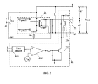
- FIG 2 is a schematic structural diagram of a voltage regulating circuit according to another embodiment of the present invention. As shown in FIG 2 , the voltage regulating circuit in this embodiment is a specific circuit structure.
- output ends a and b of a main loop unit output a first voltage signal Us' whose voltage value is equal to a voltage value of a voltage source 20.
- a voltage boosting unit in this embodiment is a half-bridge converter 21, as shown in a circuit diagram in a dotted box in the figure.
- the half-bridge converter 21 includes a rectifying unit inside, an input end of the half-bridge converter 21 is connected to the voltage source 20, and output ends c and d of the half-bridge converter 21 are configured to output a second voltage signal ⁇ U that is obtained after conversion.
- a half-bridge converter is used as a voltage boosting unit.
- a transformer in the half-bridge converter shown in FIG 2 primarily uses a half-bridge circuit and secondly uses a full-wave rectifier, and preferably, the full-wave rectifier may be a full-wave diode rectifier.
- a short-circuit switch 22 is disposed between the output ends c and d of the half-bridge converter, and closing and opening of the short-circuit switch 22 are controlled by using a relay 234 in a switching control unit 23.
- an output signal of the voltage regulating circuit is a sum of the first voltage signal Us' and the second voltage signal ⁇ U.
- output ends a and b of a main loop unit and output ends c and d of a voltage boosting unit may be connected in series, to enable output ends a and d of a voltage regulating circuit to output Us'+ ⁇ U.
- the voltage source is enabled to output, by using the voltage regulating circuit, a voltage signal that meets a requirement of a device.
- the switching control unit 23 in this embodiment mainly includes: a first sampler 231, a first voltage comparator 232, a diode, a triode 233, and a relay 234.
- the first voltage comparator 232 is configured to compare a voltage value with a first reference voltage, where the voltage value is sampled by the first sampler 231 and output by the main loop unit; and when the voltage value sampled by the first sampler is greater than or equal to the first reference voltage, the first voltage comparator 232 outputs a high level, then the diode that is connected to a base of the triode 233 outputs the high level to the base of the triode 233, to enable a collector of the triode 233 to output a signal, and then the relay 234 that is connected to the collector of the triode controls a short-circuit switch to be closed, to ensure that a voltage value of a second voltage signal output by an output end of the voltage boosting unit is zero.
- an input end of the first sampler 231 is connected to the output ends a and b of the main loop unit, and an output end of the first sampler 231 is connected to a first input end of the first voltage comparator 232.
- a second input end of the first voltage comparator 232 receives a given first reference voltage Vg, an output end of the first voltage comparator 232 is connected to an anode of the diode, a cathode of the diode is connected to the base of the triode 233, an emitter of the triode 233 is connected to the ground, and the collector is connected to the relay 234 that controls the short-circuit switch 22 of the voltage boosting unit.
- the first voltage comparator 232 receives a voltage value of the first voltage signal, where the voltage value of the first voltage signal is sampled by the first sampler 231 and output by the main loop unit, and compares the voltage value with the given first reference voltage Vg; and when the voltage value of the first voltage signal is greater than or equal to the first reference voltage Vg, the first voltage comparator 232 outputs a high level, and outputs the high level to the base of the triode 233 by using the diode that is connected to the output end of the first voltage comparator, and then controls, by using the relay 234 that is connected to the collector of the triode, the short-circuit switch 22 to be closed, to enable the output ends c and d of the voltage boosting unit to be short-circuited, where in this case, ⁇ U output by an output end of the voltage boosting unit is zero.
- the switching control unit 23 may also use another hardware circuit to control opening and closing of the short-circuit switch of the voltage boosting unit, and the switching control unit 23 of this embodiment is only used as an example for description.
- the voltage regulating circuit in this embodiment uses a half-bridge converter to output a second voltage signal, and the second voltage signal and a first voltage signal are connected in series to form an output signal of the voltage regulating circuit.
- efficiency of voltage boosting in the voltage regulating circuit in this embodiment can be improved, and power consumption of the voltage regulating circuit can be reduced, thereby reducing heat of a system in which the voltage regulating circuit is used and reducing the volume of the system.
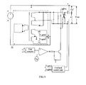
- FIG 3A is a schematic structural diagram of a voltage regulating circuit according to another embodiment of the present invention
- FIG 3B is a schematic structural diagram of a feedback control unit in a voltage regulating circuit according to another embodiment of the present invention.
- a difference between a topology of a voltage regulating circuit shown in FIG 3A and a topology of a voltage regulating circuit shown in FIG 2 lies in that: the voltage regulating circuit in this embodiment further includes a feedback control unit 24, where the feedback control unit 24 herein is mainly configured to receive an output signal Vout of the voltage regulating circuit, and regulate, according to the output signal of the voltage regulating circuit, a second voltage signal output by a voltage boosting unit.
- the feedback control unit 24 in this embodiment mainly includes: a second sampler 241, a subtracter 242, a proportion integrator 243, a second voltage comparator 244, and a pulse distributor 245, where the subtracter 242 is configured to perform a subtraction operation on a given second reference voltage and an output signal voltage Vout that is sampled by the second sampler 241 and output by the voltage regulating circuit; and the proportion integrator 243 is configured to perform integration regulation on an output signal of the subtracter 242; the second voltage comparator 244 is configured to compare an output signal of the proportion integrator 243 with a given triangular wave; and the pulse distributor 245 outputs a drive signal according to a signal output by the second voltage comparator 244, so that the voltage boosting unit regulates, according to the drive signal, a second voltage signal ⁇ U output by the voltage boosting unit.
- the second sampler 241 herein performs, by using a photocoupler, isolation sampling on an output signal that is between output ends a and d, a subtraction operation is performed, in the subtracter 242, on a sampled voltage value V f and a second reference voltage V ref , and then a voltage V com is obtained after the proportion integrator 243 performs integration regulation on the output signal of the subtracter 242.
- the second voltage comparator 244 generate a pulse width modulation (Pulse Width Modulation, PWM for short) signal after receiving V com and V _tri 246 from a triangle wave generator, and after the PWM signal passes through the pulse distributor 245, drive signals V-gate for driving the voltage boosting unit are output.
- PWM Pulse Width Modulation
- drive signals V-gate 1 and V-gate 2 output by the pulse distributor 245 herein are used to drive a field-effect transistor of the half-bridge converter (as shown in FIG 2 ); or drive signals V-gate 1, V-gate 2, V-gate 3, and V-gate 4 output by the pulse distributor 245 are used to drive a field-effect transistor of a full-bridge converter (as shown in FIG 4 ).
- the subtracter 242 receives the given second reference voltage V ref and a voltage value of the output signal of the voltage regulating circuit, where the output signal is sampled by the second sampler 241; and then the subtracter 242 performs a subtraction operation on the given second reference voltage and the voltage value output by the voltage regulating circuit, and inputs a result of the subtraction operation performed by the subtracter 242 into the proportion integrator 243, where an output end of the proportion integrator 243 is connected to a first input end of the second voltage comparator 244.
- the first input end of the second voltage comparator 244 receives an output signal of the proportion integrator 243; a second input end of the second voltage comparator 244 is connected to a triangle wave generator 246, and receives a triangle wave output by the triangle wave generator 246; and the second voltage comparator 244 compares the output signal of the proportion integrator 243 with the triangle wave, and inputs the compared output signal into the pulse distributor 245, so that the pulse distributor outputs the drive signal.
- the voltage regulating circuit in this embodiment can output a second voltage signal ⁇ U by using a voltage boosting unit, and a signal output by the voltage regulating circuit is a sum of the first voltage signal and the second voltage signal.
- the conversion efficiency of the voltage regulating circuit is high and power consumption of the voltage regulating circuit is low, and less heat is generated by the voltage regulating circuit, so that the volume of a system in which the voltage regulating circuit is included can be reduced.
- FIG. 4 and FIG 5 both are schematic diagrams of a topology of a voltage regulating circuit according to another embodiment of the present invention.
- a voltage boosting unit shown in FIG 4 is a full-bridge converter 41; and as shown in a dotted box in FIG. 4 , a transformer in the full-bridge converter shown in FIG 4 primarily uses a full-bridge circuit, secondly uses a full-wave rectifier, and preferably, uses a full-wave diode rectifier, so that the full-bridge converter shown in FIG 4 can improve the conversion efficiency of the voltage boosting unit.
- a voltage boosting unit shown in FIG 5 is a push-pull converter 51; and as shown in a dotted box in FIG 5 , a transformer in the push-pull converter shown in FIG 5 primarily uses a push-pull circuit, secondly uses a full-wave rectifier, and preferably, uses a full-wave diode rectifier, so that the push-pull converter 51 shown in FIG 5 can also improve the conversion efficiency of the voltage boosting unit.
- the voltage regulating circuit shown in FIG 4 and FIG 5 includes a switching control unit and a feedback control unit, where the switching control unit herein is basically the same as the switching control unit shown in FIG. 3A , and the feedback control unit is basically the same as the switching control unit shown in FIG. 3B , which are not described in further detail in this embodiment.
- an output end of the voltage regulating circuit shown in FIG 2 , FIG. 3A , FIG. 4 , and FIG 5 may further be disposed with an inductor (not shown in the figure) configured to perform filtering on an output signal of the voltage regulating circuit, so that the voltage regulating circuit can output a better signal.
- an inductor not shown in the figure
- the first reference voltage is 51.5V; and when a first voltage signal Us' is greater than or equal to 51.5V, a second voltage signal that can be output by the voltage boosting unit is zero, and in this case, a voltage value output by the voltage regulating circuit is Us.
- the voltage boosting unit When Us' is less than 51.5V, the voltage boosting unit outputs a second voltage signal that is not zero, and a voltage value of the second voltage signal is consistent with a difference obtained by subtracting Us from 51.5V.
- the efficiency of the voltage regulating circuit in this embodiment is greatly improved, and power consumption of the voltage regulating circuit can be reduced.
- the volume of a system in which the voltage regulating circuit is used can also be reduced.
Landscapes
- Engineering & Computer Science (AREA)
- Power Engineering (AREA)
- Dc-Dc Converters (AREA)
Abstract
Description
- Embodiments of the present invention relate to circuit technologies, and in particular, to a voltage regulating circuit.
- As a technology of integrating three networks (a telecommunications network, a cable television network, and the Internet) emerges, a mobile MBB (Modular Building Block, MBB for short) bandwidth becomes increasingly broader, which causes that a power of a radio remote unit (Radio Remote Unit, RRU for short) increases doubly, and a diameter of a cable becomes increasingly thicker because the power increases. In addition, for a relatively remote outdoor tower station, an outdoor roof station, or a relatively large-coverage indoor place, an RRU needs to have a remote capability, and in this case, a diameter of an RRU cable becomes relatively thick, so that costs of an RRU solution are increased, for example, an RRU remote terminal becomes larger, outgoing cables of a cabinet and a power distribution box are thicker, space needs to be increased, and an extra switching component is required, which are not beneficial to normalized design of a product.
- In the prior art, a voltage boosting circuit for direct voltage boosting is disclosed. In the circuit, a voltage source is connected to a converter directly, and after the voltage source is converted by the converter, a required voltage is output.
- However, by using the foregoing voltage boosting circuit, without considering a voltage value of an original voltage source, all powers of the voltage source pass through a whole converter directly, which easily causes low efficiency and high power consumption of a whole voltage boosting circuit in a process of boosting a voltage, and further brings a heat dissipation problem to a system that includes a voltage boosting circuit, so that the volume of the system is increased and costs of the system are increased.
- Embodiments of the present invention provide a voltage regulating circuit, so as to solve a problem of low efficiency and high power consumption of a voltage boosting circuit in the prior art.
- A first aspect of the present invention provides a voltage regulating circuit, including:
- a main loop unit, configured to output, according to an input signal of a voltage source, a first voltage signal whose voltage value is equal to a voltage value of the voltage source;
- a voltage boosting unit, configured to output a second voltage signal according to the input signal, where a sum of the second voltage signal and the first voltage signal forms an output signal of the voltage regulating circuit; and
- a switching control unit, configured to compare the first voltage signal with a preset first reference voltage, and when the first voltage signal is greater than or equal to the first reference voltage, control the second voltage signal output by the voltage boosting unit to be zero.
- It can be known from the foregoing technical solution that, the voltage regulating circuit in the embodiment of the present invention outputs a second voltage signal by using a voltage boosting unit, and a sum of the second voltage signal and a first voltage signal forms an output signal of the voltage regulating circuit. In this way, efficiency of voltage boosting in the voltage regulating circuit in the embodiment of the present invention can be improved, and power consumption of the voltage regulating circuit can be reduced, thereby reducing heat of a system in which the voltage regulating circuit is used and reducing the volume of the system.
- To describe the technical solutions in the embodiments of the present invention more clearly, the following briefly introduces the accompanying drawings required for describing the embodiments. Apparently, the accompanying drawings in the following description show merely some embodiments of the present invention, and persons of ordinary skill in the art may still derive other drawings from these accompanying drawings without creative efforts.
-
FIG 1 is a schematic structural diagram of a voltage regulating circuit according to an embodiment of the present invention; -
FIG 2 is a schematic diagram of a topology of a voltage regulating circuit according to another embodiment of the present invention; -
FIG 3A is a schematic diagram of a topology of a voltage regulating circuit according to another embodiment of the present invention; -
FIG 3B is a schematic structural diagram of a feedback control unit in a voltage regulating circuit according to another embodiment of the present invention; -
FIG 4 is a schematic diagram of a topology of a voltage regulating circuit according to another embodiment of the present invention; and -
FIG 5 is a schematic diagram of a topology of a voltage regulating circuit according to another embodiment of the present invention. - To make the objectives, technical solutions, and advantages of the present invention clearer, the following clearly and completely describes the technical solutions of the present invention with reference to the accompanying drawings in the embodiments of the present invention. Apparently, the following described embodiments are merely a part of the embodiments of the present invention. Based on the following described embodiments of the present invention, persons of ordinary skill in the art can obtain other embodiments which can solve the technical problem of the present invention and implement the technical effect of the present invention by equivalently altering a part of or all the technical features even without creative efforts. Apparently, the embodiments obtained by means of alteration do not depart from the scope disclosed in the present invention.
-
FIG 1 is a schematic structural diagram of a voltage regulating circuit according to an embodiment of the present invention. As shown inFIG. 1 , a voltage regulatingcircuit 9 in this embodiment includes: amain loop unit 11, avoltage boosting unit 12, and aswitching control unit 13, where
themain loop unit 11 outputs, according to an input signal (Us shown inFIG. 1 ) of avoltage source 10, a first voltage signal Us' whose voltage value is equal to a voltage value of thevoltage source 10;
thevoltage boosting unit 12 is configured to output a second voltage signal ΔU according to the input signal Us, where a sum of the second voltage signal AU and the first voltage signal Us' forms an output signal of the voltage regulatingcircuit 9; and
theswitching control unit 13 is configured to compare the first voltage signal Us' with a preset first reference voltage Vg, and when the first voltage signal Us' is greater than or equal to the first reference voltage Vg, control the second voltage signal ΔU output by the voltage boosting unit to be zero. - In this embodiment, the
voltage boosting unit 12 and themain loop unit 11 are disposed in parallel, and they share onevoltage source 10, that is, an input end of themain loop unit 11 is connected to thevoltage source 10, an input end of thevoltage boosting unit 12 is connected to thevoltage source 10, and output ends of the main loop unit 11 (a and b shown inFIG. 1 ) and output ends of the voltage boosting unit 12 (c and d shown inFIG 1 ) are connected in series to form output ends of the voltage regulating circuit 9 (a and d shown inFIG 1 ). - Particularly, in this embodiment, a short-
circuit switch 121 is disposed between the output ends c and d of thevoltage boosting unit 12, where the short-circuit switch 121 is connected to theswitching control unit 13, so that theswitching control unit 13 controls, when it is determined that the first voltage signal Us' is greater than or equal to the first reference voltage Vg, the short-circuit switch 121 to be closed, to enable a second voltage signal ΔU output by thevoltage boosting unit 12 to be zero. - Specifically, an input end of the
switching control unit 13 is connected to the output ends a and b of themain loop unit 11, receives the first voltage signal Us' output by themain loop unit 11, and theswitching control unit 13 compares the first voltage signal Us' with the preset first reference voltage Vg; and if the first voltage signal Us' is less than the first reference voltage Vg, the short-circuit switch 121 is controlled to be opened by theswitching control unit 13, so that thevoltage boosting unit 12 outputs a second voltage signal ΔU that is not zero; and if the first voltage signal Us' is greater than or equal to the first reference voltage Vg, the short-circuit switch 121 is controlled to be closed by theswitching control unit 13, that is, the output ends of thevoltage boosting unit 12 are short-circuited, to enable the second voltage signal ΔU output by thevoltage boosting unit 12 to be zero. - It should be noted that the preset first reference voltage Vg is usually 51.5V, which is a basic voltage used by an existing voltage class.
- For example, the voltage boosting unit in this embodiment may be a full-bridge converter (as shown in
FIG. 4 ), a half-bridge converter (as shown inFIG. 2 ), a push-pull converter (as shown inFIG 5 ), a forward converter (not shown in the figure) or a flyback converter (not shown in the figure), where an input end of the push-pull converter is connected to the voltage source, and is configured to convert the input signal Us of the voltage source into a required second voltage signal ΔU according to the input signal Us of the voltage source. - In an actual application, the voltage regulating
circuit 9 further includes a feedback control unit (as shown inFIG. 3 ), configured to regulate, according to the output signal of the voltage regulatingcircuit 9, the second voltage signal ΔU output by thevoltage boosting unit 12. - In other words, the feedback control unit is configured to receive the output signal Vout of the voltage regulating
circuit 9, and regulate, according to the output signal Vout of the voltage regulating circuit, the second voltage signal ΔU output by thevoltage boosting unit 12. In this embodiment, a voltage value and/or a pulse width of the second voltage signal ΔU is regulated according to a voltage value and/or a pulse width of the output signal Vout, to enable the second voltage signal output by thevoltage boosting unit 12 to be more stable. - It can be known from the foregoing embodiment that, the voltage regulating circuit in the embodiment of the present invention outputs a second voltage signal by using a voltage boosting unit, and a sum of the second voltage signal and a first voltage signal forms an output signal of the voltage regulating circuit. In this way, efficiency of voltage boosting in the voltage regulating circuit in this embodiment can be improved, and power consumption of the voltage regulating circuit can be reduced, thereby reducing heat of a system in which the voltage regulating circuit is used and reducing the volume of the system.
-
FIG 2 is a schematic structural diagram of a voltage regulating circuit according to another embodiment of the present invention. As shown inFIG 2 , the voltage regulating circuit in this embodiment is a specific circuit structure. - In this embodiment, output ends a and b of a main loop unit output a first voltage signal Us' whose voltage value is equal to a voltage value of a
voltage source 20. - A voltage boosting unit in this embodiment is a half-
bridge converter 21, as shown in a circuit diagram in a dotted box in the figure. In an actual application, the half-bridge converter 21 includes a rectifying unit inside, an input end of the half-bridge converter 21 is connected to thevoltage source 20, and output ends c and d of the half-bridge converter 21 are configured to output a second voltage signal ΔU that is obtained after conversion. - It should be noted that, in this embodiment, a half-bridge converter is used as a voltage boosting unit. A transformer in the half-bridge converter shown in
FIG 2 primarily uses a half-bridge circuit and secondly uses a full-wave rectifier, and preferably, the full-wave rectifier may be a full-wave diode rectifier. - Certainly, a short-
circuit switch 22 is disposed between the output ends c and d of the half-bridge converter, and closing and opening of the short-circuit switch 22 are controlled by using a relay 234 in aswitching control unit 23. - In this embodiment, an output signal of the voltage regulating circuit is a sum of the first voltage signal Us' and the second voltage signal ΔU. In an actual circuit, output ends a and b of a main loop unit and output ends c and d of a voltage boosting unit may be connected in series, to enable output ends a and d of a voltage regulating circuit to output Us'+ΔU. In this embodiment, the voltage source is enabled to output, by using the voltage regulating circuit, a voltage signal that meets a requirement of a device.
- The voltage regulating circuit in this embodiment is used as an example for description. Assuming that a required power of the voltage regulating circuit is 1000W and a required voltage of the voltage regulating circuit is 51V, in this case, a current is 1000W/51V=19.6A.
- When a voltage of the voltage source is Us=38V, the voltage boosting unit needs to output a second voltage signal ΔU=51V-38V=13V. In addition, a power output by the voltage boosting unit is 13V* 19.6A=255W.
- Assuming that the conversion efficiency of a voltage boosting unit outputting 255W is 93%, an equivalent efficiency of a voltage regulating circuit outputting 1000W is: 1-[255(1-93%)/1000]=98.2. Therefore, the overall conversion efficiency of the voltage regulating circuit in this embodiment is improved effectively, and compared with that in the prior art, power consumption of the voltage boosting unit herein is quite low.
- Further, in an actual application, it is relatively easy to set a voltage boosting unit of 255W.
- In addition, it can be seen from
FIG. 2 that, theswitching control unit 23 in this embodiment mainly includes: afirst sampler 231, afirst voltage comparator 232, a diode, atriode 233, and a relay 234. - The
first voltage comparator 232 is configured to compare a voltage value with a first reference voltage, where the voltage value is sampled by thefirst sampler 231 and output by the main loop unit; and when the voltage value sampled by the first sampler is greater than or equal to the first reference voltage, thefirst voltage comparator 232 outputs a high level, then the diode that is connected to a base of thetriode 233 outputs the high level to the base of thetriode 233, to enable a collector of thetriode 233 to output a signal, and then the relay 234 that is connected to the collector of the triode controls a short-circuit switch to be closed, to ensure that a voltage value of a second voltage signal output by an output end of the voltage boosting unit is zero. - Certainly, an input end of the
first sampler 231 is connected to the output ends a and b of the main loop unit, and an output end of thefirst sampler 231 is connected to a first input end of thefirst voltage comparator 232. - A second input end of the
first voltage comparator 232 receives a given first reference voltage Vg, an output end of thefirst voltage comparator 232 is connected to an anode of the diode, a cathode of the diode is connected to the base of thetriode 233, an emitter of thetriode 233 is connected to the ground, and the collector is connected to the relay 234 that controls the short-circuit switch 22 of the voltage boosting unit. - In other words, the
first voltage comparator 232 receives a voltage value of the first voltage signal, where the voltage value of the first voltage signal is sampled by thefirst sampler 231 and output by the main loop unit, and compares the voltage value with the given first reference voltage Vg; and when the voltage value of the first voltage signal is greater than or equal to the first reference voltage Vg, thefirst voltage comparator 232 outputs a high level, and outputs the high level to the base of thetriode 233 by using the diode that is connected to the output end of the first voltage comparator, and then controls, by using the relay 234 that is connected to the collector of the triode, the short-circuit switch 22 to be closed, to enable the output ends c and d of the voltage boosting unit to be short-circuited, where in this case, ΔU output by an output end of the voltage boosting unit is zero. - Certainly, in another embodiment, the switching
control unit 23 may also use another hardware circuit to control opening and closing of the short-circuit switch of the voltage boosting unit, and the switchingcontrol unit 23 of this embodiment is only used as an example for description. - It can be known from the foregoing embodiment that, the voltage regulating circuit in this embodiment uses a half-bridge converter to output a second voltage signal, and the second voltage signal and a first voltage signal are connected in series to form an output signal of the voltage regulating circuit. In this way, efficiency of voltage boosting in the voltage regulating circuit in this embodiment can be improved, and power consumption of the voltage regulating circuit can be reduced, thereby reducing heat of a system in which the voltage regulating circuit is used and reducing the volume of the system.
-
FIG 3A is a schematic structural diagram of a voltage regulating circuit according to another embodiment of the present invention, andFIG 3B is a schematic structural diagram of a feedback control unit in a voltage regulating circuit according to another embodiment of the present invention. As shown inFIG. 3A and FIG 3B , a difference between a topology of a voltage regulating circuit shown inFIG 3A and a topology of a voltage regulating circuit shown inFIG 2 lies in that: the voltage regulating circuit in this embodiment further includes afeedback control unit 24, where thefeedback control unit 24 herein is mainly configured to receive an output signal Vout of the voltage regulating circuit, and regulate, according to the output signal of the voltage regulating circuit, a second voltage signal output by a voltage boosting unit. - The
feedback control unit 24 in this embodiment mainly includes: asecond sampler 241, asubtracter 242, aproportion integrator 243, asecond voltage comparator 244, and apulse distributor 245, where
thesubtracter 242 is configured to perform a subtraction operation on a given second reference voltage and an output signal voltage Vout that is sampled by thesecond sampler 241 and output by the voltage regulating circuit; and
theproportion integrator 243 is configured to perform integration regulation on an output signal of thesubtracter 242; thesecond voltage comparator 244 is configured to compare an output signal of theproportion integrator 243 with a given triangular wave; and thepulse distributor 245 outputs a drive signal according to a signal output by thesecond voltage comparator 244, so that the voltage boosting unit regulates, according to the drive signal, a second voltage signal ΔU output by the voltage boosting unit. - In other words, the
second sampler 241 herein performs, by using a photocoupler, isolation sampling on an output signal that is between output ends a and d, a subtraction operation is performed, in thesubtracter 242, on a sampled voltage value Vf and a second reference voltage Vref, and then a voltage Vcom is obtained after theproportion integrator 243 performs integration regulation on the output signal of thesubtracter 242. - The
second voltage comparator 244 generate a pulse width modulation (Pulse Width Modulation, PWM for short) signal after receiving Vcom andV _tri246 from a triangle wave generator, and after the PWM signal passes through thepulse distributor 245, drive signals V-gate for driving the voltage boosting unit are output. For example, drive signals V-gate 1 and V-gate 2 output by thepulse distributor 245 herein are used to drive a field-effect transistor of the half-bridge converter (as shown inFIG 2 ); or drive signals V-gate 1, V-gate 2, V-gate 3, and V-gate 4 output by thepulse distributor 245 are used to drive a field-effect transistor of a full-bridge converter (as shown inFIG 4 ). - It may be understood that when an output voltage between the output ends a and d of the voltage regulating circuit increases, the drive signals V-gate 1 and V-gate 2 decrease, to ensure that a voltage of the whole voltage regulating circuit is stable and reliable.
- In other words, the
subtracter 242 receives the given second reference voltage Vref and a voltage value of the output signal of the voltage regulating circuit, where the output signal is sampled by thesecond sampler 241; and then thesubtracter 242 performs a subtraction operation on the given second reference voltage and the voltage value output by the voltage regulating circuit, and inputs a result of the subtraction operation performed by thesubtracter 242 into theproportion integrator 243, where an output end of theproportion integrator 243 is connected to a first input end of thesecond voltage comparator 244. - The first input end of the
second voltage comparator 244 receives an output signal of theproportion integrator 243; a second input end of thesecond voltage comparator 244 is connected to atriangle wave generator 246, and receives a triangle wave output by thetriangle wave generator 246; and thesecond voltage comparator 244 compares the output signal of theproportion integrator 243 with the triangle wave, and inputs the compared output signal into thepulse distributor 245, so that the pulse distributor outputs the drive signal. - It can be known from the foregoing embodiment that, when a first voltage signal Us' output by a main loop unit is less than or equal to a preset first reference voltage, the voltage regulating circuit in this embodiment can output a second voltage signal ΔU by using a voltage boosting unit, and a signal output by the voltage regulating circuit is a sum of the first voltage signal and the second voltage signal. In this embodiment, the conversion efficiency of the voltage regulating circuit is high and power consumption of the voltage regulating circuit is low, and less heat is generated by the voltage regulating circuit, so that the volume of a system in which the voltage regulating circuit is included can be reduced.
-
FIG. 4 andFIG 5 both are schematic diagrams of a topology of a voltage regulating circuit according to another embodiment of the present invention. A voltage boosting unit shown inFIG 4 is a full-bridge converter 41; and as shown in a dotted box inFIG. 4 , a transformer in the full-bridge converter shown inFIG 4 primarily uses a full-bridge circuit, secondly uses a full-wave rectifier, and preferably, uses a full-wave diode rectifier, so that the full-bridge converter shown inFIG 4 can improve the conversion efficiency of the voltage boosting unit. - A voltage boosting unit shown in
FIG 5 is a push-pull converter 51; and as shown in a dotted box inFIG 5 , a transformer in the push-pull converter shown inFIG 5 primarily uses a push-pull circuit, secondly uses a full-wave rectifier, and preferably, uses a full-wave diode rectifier, so that the push-pull converter 51 shown inFIG 5 can also improve the conversion efficiency of the voltage boosting unit. - In addition, the voltage regulating circuit shown in
FIG 4 andFIG 5 includes a switching control unit and a feedback control unit, where the switching control unit herein is basically the same as the switching control unit shown inFIG. 3A , and the feedback control unit is basically the same as the switching control unit shown inFIG. 3B , which are not described in further detail in this embodiment. - Preferably, an output end of the voltage regulating circuit shown in
FIG 2 ,FIG. 3A ,FIG. 4 , andFIG 5 may further be disposed with an inductor (not shown in the figure) configured to perform filtering on an output signal of the voltage regulating circuit, so that the voltage regulating circuit can output a better signal. - Generally, the first reference voltage is 51.5V; and when a first voltage signal Us' is greater than or equal to 51.5V, a second voltage signal that can be output by the voltage boosting unit is zero, and in this case, a voltage value output by the voltage regulating circuit is Us.
- When Us' is less than 51.5V, the voltage boosting unit outputs a second voltage signal that is not zero, and a voltage value of the second voltage signal is consistent with a difference obtained by subtracting Us from 51.5V.
- Compared with that in the prior art, the efficiency of the voltage regulating circuit in this embodiment is greatly improved, and power consumption of the voltage regulating circuit can be reduced. Correspondingly, in this embodiment, the volume of a system in which the voltage regulating circuit is used can also be reduced.
- Finally, it should be noted that the foregoing embodiments are merely intended for describing the technical solutions of the present invention, but not for limiting the present invention. Although the present invention is described in detail with reference to the foregoing embodiments, persons of ordinary skill in the art should understand that they may still make modifications to the technical solutions described in the foregoing embodiments or make equivalent replacements to some or all technical features thereof, as long as such modifications or replacements do not cause the essence of corresponding technical solutions to depart from the scope of the technical solutions of the embodiments of the present invention.
Claims (7)
- A voltage regulating circuit, comprising:a main loop unit, configured to output, according to an input signal of a voltage source, a first voltage signal whose voltage value is equal to a voltage value of the voltage source;a voltage boosting unit, configured to output a second voltage signal according to the input signal, wherein a sum of the second voltage signal and the first voltage signal forms an output signal of the voltage regulating circuit; anda switching control unit, configured to compare the first voltage signal with a preset first reference voltage, and when the first voltage signal is greater than or equal to the first reference voltage, control the second voltage signal output by the voltage boosting unit to be zero.
- The voltage regulating circuit according to claim 1, further comprising:a feedback control unit, configured to regulate, according to the output signal of the voltage regulating circuit, the second voltage signal output by the voltage boosting unit.
- The voltage regulating circuit according to claim 1 or 2, wherein the voltage boosting unit specifically is:a full-bridge converter, a half-bridge converter, a push-pull converter, a forward converter or a flyback converter.
- The voltage regulating circuit according to any one of claims 1 to 3, wherein:an output end of the voltage boosting unit is further disposed with a short-circuit switch; andthe short-circuit switch is connected to the switching control unit, so that the switching control unit controls, when it is determined that the first voltage signal is greater than or equal to the first reference voltage, the short-circuit switch to be closed, to enable the second voltage signal output by the voltage boosting unit to be zero.
- The voltage regulating circuit according to any one of claims 1 to 4, wherein the switching control unit comprises: a first sampler, a first voltage comparator, a diode, a triode, and a relay, wherein
the first voltage comparator is configured to compare a voltage value with the first reference voltage, wherein the voltage value is sampled by the first sampler and output by the main loop unit; and
when the voltage value sampled by the first sampler is greater than or equal to the first reference voltage, the first voltage comparator outputs a high level, and then the diode that is connected to a base of the triode outputs the high level to the base, so that the relay that is connected to a collector of the triode controls the short-circuit switch to be closed. - The voltage regulating circuit according to any one of claims 2 to 6, wherein the feedback control unit comprises: a second sampler, a subtracter, a proportion integrator, a second voltage comparator, and a pulse distributor, wherein
the subtracter is configured to perform a subtraction operation on a given second reference voltage and an output signal that is sampled by the second sampler and output by the voltage regulating circuit;
the proportion integrator is configured to perform integration regulation on an output signal of the subtracter;
the second voltage comparator is configured to compare an output signal of the proportion integrator with a given triangular wave; and
the pulse distributor outputs a drive signal according to a signal output by the second voltage comparator, so that the voltage boosting unit regulates, according to the drive signal, the second voltage signal output by the voltage boosting unit. - The voltage regulating circuit according to any one of claims 1 to 6, wherein an output end of the voltage regulating circuit is further disposed with an inductor configured to perform filtering on the output signal of the voltage regulating circuit.
Applications Claiming Priority (2)
| Application Number | Priority Date | Filing Date | Title |
|---|---|---|---|
| CN201210124386.8A CN102655377B (en) | 2012-04-25 | 2012-04-25 | voltage adjustment circuit |
| PCT/CN2012/083667 WO2013159499A1 (en) | 2012-04-25 | 2012-10-29 | Voltage regulating circuit |
Publications (3)
| Publication Number | Publication Date |
|---|---|
| EP2833532A1 true EP2833532A1 (en) | 2015-02-04 |
| EP2833532A4 EP2833532A4 (en) | 2015-08-26 |
| EP2833532B1 EP2833532B1 (en) | 2024-09-25 |
Family
ID=46730928
Family Applications (1)
| Application Number | Title | Priority Date | Filing Date |
|---|---|---|---|
| EP12875573.3A Active EP2833532B1 (en) | 2012-04-25 | 2012-10-29 | Voltage regulating circuit |
Country Status (3)
| Country | Link |
|---|---|
| EP (1) | EP2833532B1 (en) |
| CN (1) | CN102655377B (en) |
| WO (1) | WO2013159499A1 (en) |
Cited By (1)
| Publication number | Priority date | Publication date | Assignee | Title |
|---|---|---|---|---|
| WO2019076874A1 (en) * | 2017-10-16 | 2019-04-25 | Danmarks Tekniske Universitet | A dc-dc converter assembly |
Families Citing this family (4)
| Publication number | Priority date | Publication date | Assignee | Title |
|---|---|---|---|---|
| CN102655377B (en) * | 2012-04-25 | 2015-05-27 | 华为技术有限公司 | voltage adjustment circuit |
| CN106558996B (en) * | 2015-09-30 | 2020-09-08 | 株式会社村田制作所 | Improved DC-DC voltage transformation device for obtaining constant output voltage |
| CN106877709A (en) * | 2017-03-15 | 2017-06-20 | 中冶华天南京电气工程技术有限公司 | One kind is used for high voltage converter pre-charging device and method |
| US10457150B2 (en) * | 2017-06-08 | 2019-10-29 | Ford Global Technologies, Llc | Voltage stack-up converter for electrified vehicle |
Family Cites Families (13)
| Publication number | Priority date | Publication date | Assignee | Title |
|---|---|---|---|---|
| JPS55136870A (en) * | 1979-04-10 | 1980-10-25 | Toshiba Corp | Voltage conversion type power supply |
| CN1121077C (en) * | 1998-07-22 | 2003-09-10 | 大连新源动力股份有限公司 | Fuel cell stack output voltage adjustment method and output voltage adjustable fuel cell stack |
| JP3885771B2 (en) * | 2003-06-24 | 2007-02-28 | 株式会社デンソー | Power system |
| CN100355194C (en) * | 2004-03-08 | 2007-12-12 | 耿宪温 | Topological structure of switch power supply changer |
| CN101060746B (en) * | 2007-04-05 | 2011-08-10 | 深圳麦格米特电气股份有限公司 | A fluorescent lamp drive power supply |
| CN101483390B (en) * | 2008-01-07 | 2011-07-06 | 光宝科技股份有限公司 | Power supply device with adjustable output voltage |
| CN201204546Y (en) * | 2008-04-15 | 2009-03-04 | 中兴通讯股份有限公司 | DC input voltage processing circuit |
| CN101673938B (en) * | 2009-09-29 | 2012-06-27 | 杭州士兰微电子股份有限公司 | Soft Recovery Control Circuit for Output Short Circuit and Its Application in DC-DC Converter |
| GB2476508B (en) * | 2009-12-23 | 2013-08-21 | Control Tech Ltd | Voltage compensation for photovoltaic generator systems |
| CN102214994A (en) * | 2010-04-07 | 2011-10-12 | 上海航锐电源科技有限公司 | Input-series and output-series boost converter, voltage-equalizing and current-equalizing control circuit and voltage-equalizing and current-equalizing control method |
| CN201985758U (en) * | 2011-04-20 | 2011-09-21 | 南京博兰得电子科技有限公司 | DC-DC (direct current-direct current) converter |
| US8330299B2 (en) * | 2011-06-29 | 2012-12-11 | General Electric Company | DC to DC power converters and methods of controlling the same |
| CN102655377B (en) * | 2012-04-25 | 2015-05-27 | 华为技术有限公司 | voltage adjustment circuit |
-
2012
- 2012-04-25 CN CN201210124386.8A patent/CN102655377B/en active Active
- 2012-10-29 WO PCT/CN2012/083667 patent/WO2013159499A1/en not_active Ceased
- 2012-10-29 EP EP12875573.3A patent/EP2833532B1/en active Active
Cited By (1)
| Publication number | Priority date | Publication date | Assignee | Title |
|---|---|---|---|---|
| WO2019076874A1 (en) * | 2017-10-16 | 2019-04-25 | Danmarks Tekniske Universitet | A dc-dc converter assembly |
Also Published As
| Publication number | Publication date |
|---|---|
| EP2833532A4 (en) | 2015-08-26 |
| WO2013159499A1 (en) | 2013-10-31 |
| CN102655377B (en) | 2015-05-27 |
| EP2833532B1 (en) | 2024-09-25 |
| CN102655377A (en) | 2012-09-05 |
Similar Documents
| Publication | Publication Date | Title |
|---|---|---|
| Cao et al. | Wide voltage gain range LLC DC/DC topologies: State-of-the-art | |
| CN101635511B (en) | Switch voltage stabilizing circuit with frequency spectrum shaping function and method | |
| WO2021253876A1 (en) | Control method for photovoltaic rapid switching-off system, and application apparatus and system therefor | |
| EP2685620B1 (en) | Bidirectional dc-dc converter, and power source system | |
| US20100177536A1 (en) | Dc-dc power supply apparatus method for improving dc-dc power supply apparatus | |
| US10944283B2 (en) | Distributed single-stage on-board charging device and method thereof | |
| EP2975753B1 (en) | A three-level converter | |
| CN104991597A (en) | Peak current control circuit | |
| EP2833532B1 (en) | Voltage regulating circuit | |
| US12143022B2 (en) | Control circuit for controlling a power switch in a switching power supply circuit for improved EMI performance | |
| CN106655785A (en) | Bidirectional hybrid bridge DC-DC converter and half-cycle volt-second area balance control method | |
| WO2022100196A1 (en) | Power supply, power supply method, and computer storage medium | |
| CN110912405A (en) | Four-switch buck-boost converter based on voltage mode control | |
| TWI794329B (en) | Dc-to-ac power converter and isolated dc-to-dc converter suitable to be used in the dc-to-ac power converter | |
| CN113726132A (en) | Flyback converter for controlling change of conduction time | |
| US20080192512A1 (en) | Direct current to direct current converter | |
| EP4518124A1 (en) | Direct-current power converter and direct-current power conversion system | |
| CN113765365A (en) | A kind of control method of switching power supply and switching power supply | |
| CN203574903U (en) | High-power factor constant current control circuit and LED lighting equipment | |
| CN107147325B (en) | Current feed type high-power pulse current source | |
| CN109494997A (en) | A kind of high frequency switch power based on MOSFET pipe | |
| CN112993971A (en) | Bipolar bidirectional DC-DC converter with function of inhibiting direct-current voltage unbalance | |
| CN119602603A (en) | A modulation mode switching synchronous rectification soft switching step-down constant voltage power supply | |
| CN108633139B (en) | Power supply device with two paths of stable outputs and control method thereof | |
| CN115483832B (en) | Voltage conversion module, power supply system and related equipment |
Legal Events
| Date | Code | Title | Description |
|---|---|---|---|
| PUAI | Public reference made under article 153(3) epc to a published international application that has entered the european phase |
Free format text: ORIGINAL CODE: 0009012 |
|
| 17P | Request for examination filed |
Effective date: 20141031 |
|
| AK | Designated contracting states |
Kind code of ref document: A1 Designated state(s): AL AT BE BG CH CY CZ DE DK EE ES FI FR GB GR HR HU IE IS IT LI LT LU LV MC MK MT NL NO PL PT RO RS SE SI SK SM TR |
|
| AX | Request for extension of the european patent |
Extension state: BA ME |
|
| DAX | Request for extension of the european patent (deleted) | ||
| RA4 | Supplementary search report drawn up and despatched (corrected) |
Effective date: 20150727 |
|
| RIC1 | Information provided on ipc code assigned before grant |
Ipc: H02M 3/337 20060101ALI20150721BHEP Ipc: H02M 1/00 20070101ALN20150721BHEP Ipc: H02M 3/335 20060101AFI20150721BHEP |
|
| STAA | Information on the status of an ep patent application or granted ep patent |
Free format text: STATUS: EXAMINATION IS IN PROGRESS |
|
| 17Q | First examination report despatched |
Effective date: 20170725 |
|
| APBK | Appeal reference recorded |
Free format text: ORIGINAL CODE: EPIDOSNREFNE |
|
| APBN | Date of receipt of notice of appeal recorded |
Free format text: ORIGINAL CODE: EPIDOSNNOA2E |
|
| APAV | Appeal reference deleted |
Free format text: ORIGINAL CODE: EPIDOSDREFNE |
|
| APBR | Date of receipt of statement of grounds of appeal recorded |
Free format text: ORIGINAL CODE: EPIDOSNNOA3E |
|
| APBT | Appeal procedure closed |
Free format text: ORIGINAL CODE: EPIDOSNNOA9E |
|
| GRAP | Despatch of communication of intention to grant a patent |
Free format text: ORIGINAL CODE: EPIDOSNIGR1 |
|
| STAA | Information on the status of an ep patent application or granted ep patent |
Free format text: STATUS: GRANT OF PATENT IS INTENDED |
|
| RIC1 | Information provided on ipc code assigned before grant |
Ipc: H02M 1/00 20060101ALN20240424BHEP Ipc: H02M 3/337 20060101ALI20240424BHEP Ipc: H02M 3/335 20060101AFI20240424BHEP |
|
| INTG | Intention to grant announced |
Effective date: 20240510 |
|
| GRAS | Grant fee paid |
Free format text: ORIGINAL CODE: EPIDOSNIGR3 |
|
| GRAA | (expected) grant |
Free format text: ORIGINAL CODE: 0009210 |
|
| STAA | Information on the status of an ep patent application or granted ep patent |
Free format text: STATUS: THE PATENT HAS BEEN GRANTED |
|
| AK | Designated contracting states |
Kind code of ref document: B1 Designated state(s): AL AT BE BG CH CY CZ DE DK EE ES FI FR GB GR HR HU IE IS IT LI LT LU LV MC MK MT NL NO PL PT RO RS SE SI SK SM TR |
|
| REG | Reference to a national code |
Ref country code: GB Ref legal event code: FG4D |
|
| REG | Reference to a national code |
Ref country code: CH Ref legal event code: EP |
|
| REG | Reference to a national code |
Ref country code: DE Ref legal event code: R096 Ref document number: 602012081092 Country of ref document: DE |
|
| REG | Reference to a national code |
Ref country code: IE Ref legal event code: FG4D |
|
| REG | Reference to a national code |
Ref country code: LT Ref legal event code: MG9D |
|
| PG25 | Lapsed in a contracting state [announced via postgrant information from national office to epo] |
Ref country code: NO Free format text: LAPSE BECAUSE OF FAILURE TO SUBMIT A TRANSLATION OF THE DESCRIPTION OR TO PAY THE FEE WITHIN THE PRESCRIBED TIME-LIMIT Effective date: 20241225 |
|
| PG25 | Lapsed in a contracting state [announced via postgrant information from national office to epo] |
Ref country code: GR Free format text: LAPSE BECAUSE OF FAILURE TO SUBMIT A TRANSLATION OF THE DESCRIPTION OR TO PAY THE FEE WITHIN THE PRESCRIBED TIME-LIMIT Effective date: 20241226 Ref country code: FI Free format text: LAPSE BECAUSE OF FAILURE TO SUBMIT A TRANSLATION OF THE DESCRIPTION OR TO PAY THE FEE WITHIN THE PRESCRIBED TIME-LIMIT Effective date: 20240925 |
|
| PG25 | Lapsed in a contracting state [announced via postgrant information from national office to epo] |
Ref country code: BG Free format text: LAPSE BECAUSE OF FAILURE TO SUBMIT A TRANSLATION OF THE DESCRIPTION OR TO PAY THE FEE WITHIN THE PRESCRIBED TIME-LIMIT Effective date: 20240925 |
|
| PG25 | Lapsed in a contracting state [announced via postgrant information from national office to epo] |
Ref country code: LV Free format text: LAPSE BECAUSE OF FAILURE TO SUBMIT A TRANSLATION OF THE DESCRIPTION OR TO PAY THE FEE WITHIN THE PRESCRIBED TIME-LIMIT Effective date: 20240925 |
|
| PG25 | Lapsed in a contracting state [announced via postgrant information from national office to epo] |
Ref country code: RS Free format text: LAPSE BECAUSE OF FAILURE TO SUBMIT A TRANSLATION OF THE DESCRIPTION OR TO PAY THE FEE WITHIN THE PRESCRIBED TIME-LIMIT Effective date: 20241225 |
|
| REG | Reference to a national code |
Ref country code: NL Ref legal event code: MP Effective date: 20240925 |
|
| PG25 | Lapsed in a contracting state [announced via postgrant information from national office to epo] |
Ref country code: RS Free format text: LAPSE BECAUSE OF FAILURE TO SUBMIT A TRANSLATION OF THE DESCRIPTION OR TO PAY THE FEE WITHIN THE PRESCRIBED TIME-LIMIT Effective date: 20241225 Ref country code: NO Free format text: LAPSE BECAUSE OF FAILURE TO SUBMIT A TRANSLATION OF THE DESCRIPTION OR TO PAY THE FEE WITHIN THE PRESCRIBED TIME-LIMIT Effective date: 20241225 Ref country code: LV Free format text: LAPSE BECAUSE OF FAILURE TO SUBMIT A TRANSLATION OF THE DESCRIPTION OR TO PAY THE FEE WITHIN THE PRESCRIBED TIME-LIMIT Effective date: 20240925 Ref country code: GR Free format text: LAPSE BECAUSE OF FAILURE TO SUBMIT A TRANSLATION OF THE DESCRIPTION OR TO PAY THE FEE WITHIN THE PRESCRIBED TIME-LIMIT Effective date: 20241226 Ref country code: FI Free format text: LAPSE BECAUSE OF FAILURE TO SUBMIT A TRANSLATION OF THE DESCRIPTION OR TO PAY THE FEE WITHIN THE PRESCRIBED TIME-LIMIT Effective date: 20240925 Ref country code: BG Free format text: LAPSE BECAUSE OF FAILURE TO SUBMIT A TRANSLATION OF THE DESCRIPTION OR TO PAY THE FEE WITHIN THE PRESCRIBED TIME-LIMIT Effective date: 20240925 |
|
| REG | Reference to a national code |
Ref country code: AT Ref legal event code: MK05 Ref document number: 1727498 Country of ref document: AT Kind code of ref document: T Effective date: 20240925 |
|
| PG25 | Lapsed in a contracting state [announced via postgrant information from national office to epo] |
Ref country code: NL Free format text: LAPSE BECAUSE OF FAILURE TO SUBMIT A TRANSLATION OF THE DESCRIPTION OR TO PAY THE FEE WITHIN THE PRESCRIBED TIME-LIMIT Effective date: 20240925 |
|
| PG25 | Lapsed in a contracting state [announced via postgrant information from national office to epo] |
Ref country code: IS Free format text: LAPSE BECAUSE OF FAILURE TO SUBMIT A TRANSLATION OF THE DESCRIPTION OR TO PAY THE FEE WITHIN THE PRESCRIBED TIME-LIMIT Effective date: 20250125 Ref country code: PT Free format text: LAPSE BECAUSE OF FAILURE TO SUBMIT A TRANSLATION OF THE DESCRIPTION OR TO PAY THE FEE WITHIN THE PRESCRIBED TIME-LIMIT Effective date: 20250127 |
|
| PG25 | Lapsed in a contracting state [announced via postgrant information from national office to epo] |
Ref country code: RO Free format text: LAPSE BECAUSE OF FAILURE TO SUBMIT A TRANSLATION OF THE DESCRIPTION OR TO PAY THE FEE WITHIN THE PRESCRIBED TIME-LIMIT Effective date: 20240925 Ref country code: SM Free format text: LAPSE BECAUSE OF FAILURE TO SUBMIT A TRANSLATION OF THE DESCRIPTION OR TO PAY THE FEE WITHIN THE PRESCRIBED TIME-LIMIT Effective date: 20240925 |
|
| PG25 | Lapsed in a contracting state [announced via postgrant information from national office to epo] |
Ref country code: ES Free format text: LAPSE BECAUSE OF FAILURE TO SUBMIT A TRANSLATION OF THE DESCRIPTION OR TO PAY THE FEE WITHIN THE PRESCRIBED TIME-LIMIT Effective date: 20240925 |
|
| PG25 | Lapsed in a contracting state [announced via postgrant information from national office to epo] |
Ref country code: EE Free format text: LAPSE BECAUSE OF FAILURE TO SUBMIT A TRANSLATION OF THE DESCRIPTION OR TO PAY THE FEE WITHIN THE PRESCRIBED TIME-LIMIT Effective date: 20240925 Ref country code: AT Free format text: LAPSE BECAUSE OF FAILURE TO SUBMIT A TRANSLATION OF THE DESCRIPTION OR TO PAY THE FEE WITHIN THE PRESCRIBED TIME-LIMIT Effective date: 20240925 |
|
| PG25 | Lapsed in a contracting state [announced via postgrant information from national office to epo] |
Ref country code: CZ Free format text: LAPSE BECAUSE OF FAILURE TO SUBMIT A TRANSLATION OF THE DESCRIPTION OR TO PAY THE FEE WITHIN THE PRESCRIBED TIME-LIMIT Effective date: 20240925 Ref country code: PL Free format text: LAPSE BECAUSE OF FAILURE TO SUBMIT A TRANSLATION OF THE DESCRIPTION OR TO PAY THE FEE WITHIN THE PRESCRIBED TIME-LIMIT Effective date: 20240925 |
|
| PG25 | Lapsed in a contracting state [announced via postgrant information from national office to epo] |
Ref country code: IT Free format text: LAPSE BECAUSE OF FAILURE TO SUBMIT A TRANSLATION OF THE DESCRIPTION OR TO PAY THE FEE WITHIN THE PRESCRIBED TIME-LIMIT Effective date: 20240925 Ref country code: SK Free format text: LAPSE BECAUSE OF FAILURE TO SUBMIT A TRANSLATION OF THE DESCRIPTION OR TO PAY THE FEE WITHIN THE PRESCRIBED TIME-LIMIT Effective date: 20240925 |
|
| REG | Reference to a national code |
Ref country code: CH Ref legal event code: PL |
|
| REG | Reference to a national code |
Ref country code: DE Ref legal event code: R097 Ref document number: 602012081092 Country of ref document: DE |
|
| PG25 | Lapsed in a contracting state [announced via postgrant information from national office to epo] |
Ref country code: MC Free format text: LAPSE BECAUSE OF FAILURE TO SUBMIT A TRANSLATION OF THE DESCRIPTION OR TO PAY THE FEE WITHIN THE PRESCRIBED TIME-LIMIT Effective date: 20240925 |
|
| PG25 | Lapsed in a contracting state [announced via postgrant information from national office to epo] |
Ref country code: DK Free format text: LAPSE BECAUSE OF FAILURE TO SUBMIT A TRANSLATION OF THE DESCRIPTION OR TO PAY THE FEE WITHIN THE PRESCRIBED TIME-LIMIT Effective date: 20240925 |
|
| PG25 | Lapsed in a contracting state [announced via postgrant information from national office to epo] |
Ref country code: LU Free format text: LAPSE BECAUSE OF NON-PAYMENT OF DUE FEES Effective date: 20241029 Ref country code: BE Free format text: LAPSE BECAUSE OF NON-PAYMENT OF DUE FEES Effective date: 20241031 |
|
| PG25 | Lapsed in a contracting state [announced via postgrant information from national office to epo] |
Ref country code: CH Free format text: LAPSE BECAUSE OF NON-PAYMENT OF DUE FEES Effective date: 20241031 |
|
| PLBE | No opposition filed within time limit |
Free format text: ORIGINAL CODE: 0009261 |
|
| STAA | Information on the status of an ep patent application or granted ep patent |
Free format text: STATUS: NO OPPOSITION FILED WITHIN TIME LIMIT |
|
| REG | Reference to a national code |
Ref country code: BE Ref legal event code: MM Effective date: 20241031 |
|
| GBPC | Gb: european patent ceased through non-payment of renewal fee |
Effective date: 20241225 |
|
| 26N | No opposition filed |
Effective date: 20250626 |
|
| PG25 | Lapsed in a contracting state [announced via postgrant information from national office to epo] |
Ref country code: SE Free format text: LAPSE BECAUSE OF FAILURE TO SUBMIT A TRANSLATION OF THE DESCRIPTION OR TO PAY THE FEE WITHIN THE PRESCRIBED TIME-LIMIT Effective date: 20240925 |
|
| PG25 | Lapsed in a contracting state [announced via postgrant information from national office to epo] |
Ref country code: GB Free format text: LAPSE BECAUSE OF NON-PAYMENT OF DUE FEES Effective date: 20241225 |
|
| PG25 | Lapsed in a contracting state [announced via postgrant information from national office to epo] |
Ref country code: FR Free format text: LAPSE BECAUSE OF NON-PAYMENT OF DUE FEES Effective date: 20241125 |
|
| PG25 | Lapsed in a contracting state [announced via postgrant information from national office to epo] |
Ref country code: IE Free format text: LAPSE BECAUSE OF NON-PAYMENT OF DUE FEES Effective date: 20241029 |
|
| PGFP | Annual fee paid to national office [announced via postgrant information from national office to epo] |
Ref country code: DE Payment date: 20250902 Year of fee payment: 14 |
|
| PG25 | Lapsed in a contracting state [announced via postgrant information from national office to epo] |
Ref country code: HR Free format text: LAPSE BECAUSE OF FAILURE TO SUBMIT A TRANSLATION OF THE DESCRIPTION OR TO PAY THE FEE WITHIN THE PRESCRIBED TIME-LIMIT Effective date: 20240925 |
|
| PG25 | Lapsed in a contracting state [announced via postgrant information from national office to epo] |
Ref country code: HU Free format text: LAPSE BECAUSE OF FAILURE TO SUBMIT A TRANSLATION OF THE DESCRIPTION OR TO PAY THE FEE WITHIN THE PRESCRIBED TIME-LIMIT; INVALID AB INITIO Effective date: 20121029 |
|
| PG25 | Lapsed in a contracting state [announced via postgrant information from national office to epo] |
Ref country code: CY Free format text: LAPSE BECAUSE OF FAILURE TO SUBMIT A TRANSLATION OF THE DESCRIPTION OR TO PAY THE FEE WITHIN THE PRESCRIBED TIME-LIMIT; INVALID AB INITIO Effective date: 20121029 |
|
| PG25 | Lapsed in a contracting state [announced via postgrant information from national office to epo] |
Ref country code: TR Free format text: LAPSE BECAUSE OF FAILURE TO SUBMIT A TRANSLATION OF THE DESCRIPTION OR TO PAY THE FEE WITHIN THE PRESCRIBED TIME-LIMIT Effective date: 20240925 |
|
| PG25 | Lapsed in a contracting state [announced via postgrant information from national office to epo] |
Ref country code: SI Free format text: LAPSE BECAUSE OF FAILURE TO SUBMIT A TRANSLATION OF THE DESCRIPTION OR TO PAY THE FEE WITHIN THE PRESCRIBED TIME-LIMIT Effective date: 20240925 |
|
| PG25 | Lapsed in a contracting state [announced via postgrant information from national office to epo] |
Ref country code: LT Free format text: LAPSE BECAUSE OF FAILURE TO SUBMIT A TRANSLATION OF THE DESCRIPTION OR TO PAY THE FEE WITHIN THE PRESCRIBED TIME-LIMIT Effective date: 20240925 |