EP2833427A1 - Organic electrochemical device, and method for manufacturing same - Google Patents
Organic electrochemical device, and method for manufacturing same Download PDFInfo
- Publication number
- EP2833427A1 EP2833427A1 EP20130787335 EP13787335A EP2833427A1 EP 2833427 A1 EP2833427 A1 EP 2833427A1 EP 20130787335 EP20130787335 EP 20130787335 EP 13787335 A EP13787335 A EP 13787335A EP 2833427 A1 EP2833427 A1 EP 2833427A1
- Authority
- EP
- European Patent Office
- Prior art keywords
- organic
- electrode
- electrochemical device
- layer
- intermediate layer
- Prior art date
- Legal status (The legal status is an assumption and is not a legal conclusion. Google has not performed a legal analysis and makes no representation as to the accuracy of the status listed.)
- Withdrawn
Links
- 238000000034 method Methods 0.000 title claims abstract description 23
- 238000004519 manufacturing process Methods 0.000 title abstract description 4
- 239000011368 organic material Substances 0.000 claims abstract description 79
- 239000000758 substrate Substances 0.000 claims abstract description 34
- 239000000463 material Substances 0.000 claims description 61
- 229910052751 metal Inorganic materials 0.000 claims description 16
- 239000002184 metal Substances 0.000 claims description 16
- 230000001788 irregular Effects 0.000 claims description 6
- -1 poly(3,4-ethylenedioxythiophene) Polymers 0.000 description 17
- 229920001940 conductive polymer Polymers 0.000 description 7
- 239000003575 carbonaceous material Substances 0.000 description 6
- 238000006243 chemical reaction Methods 0.000 description 6
- 238000005229 chemical vapour deposition Methods 0.000 description 6
- 239000011521 glass Substances 0.000 description 6
- 229920001467 poly(styrenesulfonates) Polymers 0.000 description 5
- OKTJSMMVPCPJKN-UHFFFAOYSA-N Carbon Chemical compound [C] OKTJSMMVPCPJKN-UHFFFAOYSA-N 0.000 description 4
- PXHVJJICTQNCMI-UHFFFAOYSA-N Nickel Chemical compound [Ni] PXHVJJICTQNCMI-UHFFFAOYSA-N 0.000 description 4
- XLOMVQKBTHCTTD-UHFFFAOYSA-N Zinc monoxide Chemical compound [Zn]=O XLOMVQKBTHCTTD-UHFFFAOYSA-N 0.000 description 4
- 150000001875 compounds Chemical class 0.000 description 4
- 238000000151 deposition Methods 0.000 description 4
- 229910003437 indium oxide Inorganic materials 0.000 description 4
- PJXISJQVUVHSOJ-UHFFFAOYSA-N indium(iii) oxide Chemical compound [O-2].[O-2].[O-2].[In+3].[In+3] PJXISJQVUVHSOJ-UHFFFAOYSA-N 0.000 description 4
- 230000031700 light absorption Effects 0.000 description 4
- BASFCYQUMIYNBI-UHFFFAOYSA-N platinum Chemical compound [Pt] BASFCYQUMIYNBI-UHFFFAOYSA-N 0.000 description 4
- XOLBLPGZBRYERU-UHFFFAOYSA-N tin dioxide Chemical compound O=[Sn]=O XOLBLPGZBRYERU-UHFFFAOYSA-N 0.000 description 4
- 229910001887 tin oxide Inorganic materials 0.000 description 4
- UHOVQNZJYSORNB-UHFFFAOYSA-N Benzene Chemical compound C1=CC=CC=C1 UHOVQNZJYSORNB-UHFFFAOYSA-N 0.000 description 3
- 229920001609 Poly(3,4-ethylenedioxythiophene) Polymers 0.000 description 3
- XUIMIQQOPSSXEZ-UHFFFAOYSA-N Silicon Chemical compound [Si] XUIMIQQOPSSXEZ-UHFFFAOYSA-N 0.000 description 3
- 229910052782 aluminium Inorganic materials 0.000 description 3
- XAGFODPZIPBFFR-UHFFFAOYSA-N aluminium Chemical compound [Al] XAGFODPZIPBFFR-UHFFFAOYSA-N 0.000 description 3
- 229910021419 crystalline silicon Inorganic materials 0.000 description 3
- 238000000623 plasma-assisted chemical vapour deposition Methods 0.000 description 3
- 229910052710 silicon Inorganic materials 0.000 description 3
- 239000010703 silicon Substances 0.000 description 3
- TVIVIEFSHFOWTE-UHFFFAOYSA-K tri(quinolin-8-yloxy)alumane Chemical compound [Al+3].C1=CN=C2C([O-])=CC=CC2=C1.C1=CN=C2C([O-])=CC=CC2=C1.C1=CN=C2C([O-])=CC=CC2=C1 TVIVIEFSHFOWTE-UHFFFAOYSA-K 0.000 description 3
- UJOBWOGCFQCDNV-UHFFFAOYSA-N 9H-carbazole Chemical compound C1=CC=C2C3=CC=CC=C3NC2=C1 UJOBWOGCFQCDNV-UHFFFAOYSA-N 0.000 description 2
- XMWRBQBLMFGWIX-UHFFFAOYSA-N C60 fullerene Chemical compound C12=C3C(C4=C56)=C7C8=C5C5=C9C%10=C6C6=C4C1=C1C4=C6C6=C%10C%10=C9C9=C%11C5=C8C5=C8C7=C3C3=C7C2=C1C1=C2C4=C6C4=C%10C6=C9C9=C%11C5=C5C8=C3C3=C7C1=C1C2=C4C6=C2C9=C5C3=C12 XMWRBQBLMFGWIX-UHFFFAOYSA-N 0.000 description 2
- RYGMFSIKBFXOCR-UHFFFAOYSA-N Copper Chemical compound [Cu] RYGMFSIKBFXOCR-UHFFFAOYSA-N 0.000 description 2
- BQCADISMDOOEFD-UHFFFAOYSA-N Silver Chemical compound [Ag] BQCADISMDOOEFD-UHFFFAOYSA-N 0.000 description 2
- RTAQQCXQSZGOHL-UHFFFAOYSA-N Titanium Chemical compound [Ti] RTAQQCXQSZGOHL-UHFFFAOYSA-N 0.000 description 2
- 238000010521 absorption reaction Methods 0.000 description 2
- 229910021417 amorphous silicon Inorganic materials 0.000 description 2
- 238000000231 atomic layer deposition Methods 0.000 description 2
- IOJUPLGTWVMSFF-UHFFFAOYSA-N benzothiazole Chemical compound C1=CC=C2SC=NC2=C1 IOJUPLGTWVMSFF-UHFFFAOYSA-N 0.000 description 2
- 239000006229 carbon black Substances 0.000 description 2
- 229910021393 carbon nanotube Inorganic materials 0.000 description 2
- 239000002041 carbon nanotube Substances 0.000 description 2
- 239000000919 ceramic Substances 0.000 description 2
- 239000004020 conductor Substances 0.000 description 2
- 229910052802 copper Inorganic materials 0.000 description 2
- 239000010949 copper Substances 0.000 description 2
- 239000013078 crystal Substances 0.000 description 2
- 238000005566 electron beam evaporation Methods 0.000 description 2
- PCHJSUWPFVWCPO-UHFFFAOYSA-N gold Chemical compound [Au] PCHJSUWPFVWCPO-UHFFFAOYSA-N 0.000 description 2
- 229910052737 gold Inorganic materials 0.000 description 2
- 239000010931 gold Substances 0.000 description 2
- 229910021389 graphene Inorganic materials 0.000 description 2
- 229910052738 indium Inorganic materials 0.000 description 2
- APFVFJFRJDLVQX-UHFFFAOYSA-N indium atom Chemical compound [In] APFVFJFRJDLVQX-UHFFFAOYSA-N 0.000 description 2
- 238000007735 ion beam assisted deposition Methods 0.000 description 2
- 230000001678 irradiating effect Effects 0.000 description 2
- 238000001755 magnetron sputter deposition Methods 0.000 description 2
- 238000001883 metal evaporation Methods 0.000 description 2
- 229910052759 nickel Inorganic materials 0.000 description 2
- 125000001997 phenyl group Chemical group [H]C1=C([H])C([H])=C(*)C([H])=C1[H] 0.000 description 2
- 238000005240 physical vapour deposition Methods 0.000 description 2
- 229920003023 plastic Polymers 0.000 description 2
- 239000004033 plastic Substances 0.000 description 2
- 229910052697 platinum Inorganic materials 0.000 description 2
- 229920000301 poly(3-hexylthiophene-2,5-diyl) polymer Polymers 0.000 description 2
- 229920000553 poly(phenylenevinylene) Polymers 0.000 description 2
- 229920000767 polyaniline Polymers 0.000 description 2
- 229920000642 polymer Polymers 0.000 description 2
- 239000002861 polymer material Substances 0.000 description 2
- 229920000128 polypyrrole Polymers 0.000 description 2
- 238000001552 radio frequency sputter deposition Methods 0.000 description 2
- 229910052703 rhodium Inorganic materials 0.000 description 2
- 239000010948 rhodium Substances 0.000 description 2
- MHOVAHRLVXNVSD-UHFFFAOYSA-N rhodium atom Chemical compound [Rh] MHOVAHRLVXNVSD-UHFFFAOYSA-N 0.000 description 2
- 239000004065 semiconductor Substances 0.000 description 2
- 229910052709 silver Inorganic materials 0.000 description 2
- 239000004332 silver Substances 0.000 description 2
- 239000010936 titanium Substances 0.000 description 2
- 229910052719 titanium Inorganic materials 0.000 description 2
- WFKWXMTUELFFGS-UHFFFAOYSA-N tungsten Chemical compound [W] WFKWXMTUELFFGS-UHFFFAOYSA-N 0.000 description 2
- 229910052721 tungsten Inorganic materials 0.000 description 2
- 239000010937 tungsten Substances 0.000 description 2
- 238000007740 vapor deposition Methods 0.000 description 2
- 239000011787 zinc oxide Substances 0.000 description 2
- 150000005072 1,3,4-oxadiazoles Chemical class 0.000 description 1
- BCMCBBGGLRIHSE-UHFFFAOYSA-N 1,3-benzoxazole Chemical compound C1=CC=C2OC=NC2=C1 BCMCBBGGLRIHSE-UHFFFAOYSA-N 0.000 description 1
- HYZJCKYKOHLVJF-UHFFFAOYSA-N 1H-benzimidazole Chemical compound C1=CC=C2NC=NC2=C1 HYZJCKYKOHLVJF-UHFFFAOYSA-N 0.000 description 1
- GKWLILHTTGWKLQ-UHFFFAOYSA-N 2,3-dihydrothieno[3,4-b][1,4]dioxine Chemical compound O1CCOC2=CSC=C21 GKWLILHTTGWKLQ-UHFFFAOYSA-N 0.000 description 1
- OGGKVJMNFFSDEV-UHFFFAOYSA-N 3-methyl-n-[4-[4-(n-(3-methylphenyl)anilino)phenyl]phenyl]-n-phenylaniline Chemical compound CC1=CC=CC(N(C=2C=CC=CC=2)C=2C=CC(=CC=2)C=2C=CC(=CC=2)N(C=2C=CC=CC=2)C=2C=C(C)C=CC=2)=C1 OGGKVJMNFFSDEV-UHFFFAOYSA-N 0.000 description 1
- 229920000144 PEDOT:PSS Polymers 0.000 description 1
- 239000004734 Polyphenylene sulfide Substances 0.000 description 1
- VYPSYNLAJGMNEJ-UHFFFAOYSA-N Silicium dioxide Chemical compound O=[Si]=O VYPSYNLAJGMNEJ-UHFFFAOYSA-N 0.000 description 1
- CDBYLPFSWZWCQE-UHFFFAOYSA-L Sodium Carbonate Chemical compound [Na+].[Na+].[O-]C([O-])=O CDBYLPFSWZWCQE-UHFFFAOYSA-L 0.000 description 1
- 239000007983 Tris buffer Substances 0.000 description 1
- PNEYBMLMFCGWSK-UHFFFAOYSA-N aluminium oxide Inorganic materials [O-2].[O-2].[O-2].[Al+3].[Al+3] PNEYBMLMFCGWSK-UHFFFAOYSA-N 0.000 description 1
- 239000005407 aluminoborosilicate glass Substances 0.000 description 1
- 239000005354 aluminosilicate glass Substances 0.000 description 1
- 150000004982 aromatic amines Chemical class 0.000 description 1
- UFVXQDWNSAGPHN-UHFFFAOYSA-K bis[(2-methylquinolin-8-yl)oxy]-(4-phenylphenoxy)alumane Chemical compound [Al+3].C1=CC=C([O-])C2=NC(C)=CC=C21.C1=CC=C([O-])C2=NC(C)=CC=C21.C1=CC([O-])=CC=C1C1=CC=CC=C1 UFVXQDWNSAGPHN-UHFFFAOYSA-K 0.000 description 1
- 229920001400 block copolymer Polymers 0.000 description 1
- 239000005388 borosilicate glass Substances 0.000 description 1
- 238000005137 deposition process Methods 0.000 description 1
- 238000003618 dip coating Methods 0.000 description 1
- 230000000694 effects Effects 0.000 description 1
- 239000003792 electrolyte Substances 0.000 description 1
- 229910003472 fullerene Inorganic materials 0.000 description 1
- AMGQUBHHOARCQH-UHFFFAOYSA-N indium;oxotin Chemical compound [In].[Sn]=O AMGQUBHHOARCQH-UHFFFAOYSA-N 0.000 description 1
- 238000007641 inkjet printing Methods 0.000 description 1
- 239000010416 ion conductor Substances 0.000 description 1
- 150000002500 ions Chemical class 0.000 description 1
- JFNLZVQOOSMTJK-KNVOCYPGSA-N norbornene Chemical compound C1[C@@H]2CC[C@H]1C=C2 JFNLZVQOOSMTJK-KNVOCYPGSA-N 0.000 description 1
- 230000003287 optical effect Effects 0.000 description 1
- 229920003207 poly(ethylene-2,6-naphthalate) Polymers 0.000 description 1
- 229920000172 poly(styrenesulfonic acid) Polymers 0.000 description 1
- 229920002492 poly(sulfone) Polymers 0.000 description 1
- 229920000515 polycarbonate Polymers 0.000 description 1
- 239000004417 polycarbonate Substances 0.000 description 1
- 229920000728 polyester Polymers 0.000 description 1
- 239000011112 polyethylene naphthalate Substances 0.000 description 1
- 229920000139 polyethylene terephthalate Polymers 0.000 description 1
- 239000005020 polyethylene terephthalate Substances 0.000 description 1
- 229920002098 polyfluorene Polymers 0.000 description 1
- 229920000069 polyphenylene sulfide Polymers 0.000 description 1
- 125000001567 quinoxalinyl group Chemical class N1=C(C=NC2=CC=CC=C12)* 0.000 description 1
- YYMBJDOZVAITBP-UHFFFAOYSA-N rubrene Chemical compound C1=CC=CC=C1C(C1=C(C=2C=CC=CC=2)C2=CC=CC=C2C(C=2C=CC=CC=2)=C11)=C(C=CC=C2)C2=C1C1=CC=CC=C1 YYMBJDOZVAITBP-UHFFFAOYSA-N 0.000 description 1
- 238000007650 screen-printing Methods 0.000 description 1
- 239000005361 soda-lime glass Substances 0.000 description 1
- 239000000243 solution Substances 0.000 description 1
- 239000002904 solvent Substances 0.000 description 1
- 238000001228 spectrum Methods 0.000 description 1
- 238000004528 spin coating Methods 0.000 description 1
- 150000003413 spiro compounds Chemical class 0.000 description 1
- 125000005504 styryl group Chemical group 0.000 description 1
- 238000010345 tape casting Methods 0.000 description 1
- 150000003852 triazoles Chemical class 0.000 description 1
Images


Classifications
-
- H—ELECTRICITY
- H10—SEMICONDUCTOR DEVICES; ELECTRIC SOLID-STATE DEVICES NOT OTHERWISE PROVIDED FOR
- H10K—ORGANIC ELECTRIC SOLID-STATE DEVICES
- H10K30/00—Organic devices sensitive to infrared radiation, light, electromagnetic radiation of shorter wavelength or corpuscular radiation
- H10K30/20—Organic devices sensitive to infrared radiation, light, electromagnetic radiation of shorter wavelength or corpuscular radiation comprising organic-organic junctions, e.g. donor-acceptor junctions
- H10K30/211—Organic devices sensitive to infrared radiation, light, electromagnetic radiation of shorter wavelength or corpuscular radiation comprising organic-organic junctions, e.g. donor-acceptor junctions comprising multiple junctions, e.g. double heterojunctions
-
- G—PHYSICS
- G02—OPTICS
- G02F—OPTICAL DEVICES OR ARRANGEMENTS FOR THE CONTROL OF LIGHT BY MODIFICATION OF THE OPTICAL PROPERTIES OF THE MEDIA OF THE ELEMENTS INVOLVED THEREIN; NON-LINEAR OPTICS; FREQUENCY-CHANGING OF LIGHT; OPTICAL LOGIC ELEMENTS; OPTICAL ANALOGUE/DIGITAL CONVERTERS
- G02F1/00—Devices or arrangements for the control of the intensity, colour, phase, polarisation or direction of light arriving from an independent light source, e.g. switching, gating or modulating; Non-linear optics
- G02F1/01—Devices or arrangements for the control of the intensity, colour, phase, polarisation or direction of light arriving from an independent light source, e.g. switching, gating or modulating; Non-linear optics for the control of the intensity, phase, polarisation or colour
- G02F1/15—Devices or arrangements for the control of the intensity, colour, phase, polarisation or direction of light arriving from an independent light source, e.g. switching, gating or modulating; Non-linear optics for the control of the intensity, phase, polarisation or colour based on an electrochromic effect
- G02F1/153—Constructional details
- G02F1/155—Electrodes
-
- H—ELECTRICITY
- H10—SEMICONDUCTOR DEVICES; ELECTRIC SOLID-STATE DEVICES NOT OTHERWISE PROVIDED FOR
- H10K—ORGANIC ELECTRIC SOLID-STATE DEVICES
- H10K30/00—Organic devices sensitive to infrared radiation, light, electromagnetic radiation of shorter wavelength or corpuscular radiation
- H10K30/80—Constructional details
-
- H—ELECTRICITY
- H10—SEMICONDUCTOR DEVICES; ELECTRIC SOLID-STATE DEVICES NOT OTHERWISE PROVIDED FOR
- H10K—ORGANIC ELECTRIC SOLID-STATE DEVICES
- H10K30/00—Organic devices sensitive to infrared radiation, light, electromagnetic radiation of shorter wavelength or corpuscular radiation
- H10K30/80—Constructional details
- H10K30/81—Electrodes
-
- H—ELECTRICITY
- H10—SEMICONDUCTOR DEVICES; ELECTRIC SOLID-STATE DEVICES NOT OTHERWISE PROVIDED FOR
- H10K—ORGANIC ELECTRIC SOLID-STATE DEVICES
- H10K50/00—Organic light-emitting devices
- H10K50/10—OLEDs or polymer light-emitting diodes [PLED]
- H10K50/11—OLEDs or polymer light-emitting diodes [PLED] characterised by the electroluminescent [EL] layers
-
- H—ELECTRICITY
- H10—SEMICONDUCTOR DEVICES; ELECTRIC SOLID-STATE DEVICES NOT OTHERWISE PROVIDED FOR
- H10K—ORGANIC ELECTRIC SOLID-STATE DEVICES
- H10K50/00—Organic light-emitting devices
- H10K50/10—OLEDs or polymer light-emitting diodes [PLED]
- H10K50/14—Carrier transporting layers
- H10K50/15—Hole transporting layers
-
- H—ELECTRICITY
- H10—SEMICONDUCTOR DEVICES; ELECTRIC SOLID-STATE DEVICES NOT OTHERWISE PROVIDED FOR
- H10K—ORGANIC ELECTRIC SOLID-STATE DEVICES
- H10K50/00—Organic light-emitting devices
- H10K50/10—OLEDs or polymer light-emitting diodes [PLED]
- H10K50/14—Carrier transporting layers
- H10K50/16—Electron transporting layers
-
- H—ELECTRICITY
- H10—SEMICONDUCTOR DEVICES; ELECTRIC SOLID-STATE DEVICES NOT OTHERWISE PROVIDED FOR
- H10K—ORGANIC ELECTRIC SOLID-STATE DEVICES
- H10K50/00—Organic light-emitting devices
- H10K50/80—Constructional details
- H10K50/805—Electrodes
-
- H—ELECTRICITY
- H10—SEMICONDUCTOR DEVICES; ELECTRIC SOLID-STATE DEVICES NOT OTHERWISE PROVIDED FOR
- H10K—ORGANIC ELECTRIC SOLID-STATE DEVICES
- H10K71/00—Manufacture or treatment specially adapted for the organic devices covered by this subclass
-
- H—ELECTRICITY
- H10—SEMICONDUCTOR DEVICES; ELECTRIC SOLID-STATE DEVICES NOT OTHERWISE PROVIDED FOR
- H10K—ORGANIC ELECTRIC SOLID-STATE DEVICES
- H10K30/00—Organic devices sensitive to infrared radiation, light, electromagnetic radiation of shorter wavelength or corpuscular radiation
- H10K30/30—Organic devices sensitive to infrared radiation, light, electromagnetic radiation of shorter wavelength or corpuscular radiation comprising bulk heterojunctions, e.g. interpenetrating networks of donor and acceptor material domains
-
- H—ELECTRICITY
- H10—SEMICONDUCTOR DEVICES; ELECTRIC SOLID-STATE DEVICES NOT OTHERWISE PROVIDED FOR
- H10K—ORGANIC ELECTRIC SOLID-STATE DEVICES
- H10K30/00—Organic devices sensitive to infrared radiation, light, electromagnetic radiation of shorter wavelength or corpuscular radiation
- H10K30/50—Photovoltaic [PV] devices
-
- Y—GENERAL TAGGING OF NEW TECHNOLOGICAL DEVELOPMENTS; GENERAL TAGGING OF CROSS-SECTIONAL TECHNOLOGIES SPANNING OVER SEVERAL SECTIONS OF THE IPC; TECHNICAL SUBJECTS COVERED BY FORMER USPC CROSS-REFERENCE ART COLLECTIONS [XRACs] AND DIGESTS
- Y02—TECHNOLOGIES OR APPLICATIONS FOR MITIGATION OR ADAPTATION AGAINST CLIMATE CHANGE
- Y02E—REDUCTION OF GREENHOUSE GAS [GHG] EMISSIONS, RELATED TO ENERGY GENERATION, TRANSMISSION OR DISTRIBUTION
- Y02E10/00—Energy generation through renewable energy sources
- Y02E10/50—Photovoltaic [PV] energy
- Y02E10/549—Organic PV cells
-
- Y—GENERAL TAGGING OF NEW TECHNOLOGICAL DEVELOPMENTS; GENERAL TAGGING OF CROSS-SECTIONAL TECHNOLOGIES SPANNING OVER SEVERAL SECTIONS OF THE IPC; TECHNICAL SUBJECTS COVERED BY FORMER USPC CROSS-REFERENCE ART COLLECTIONS [XRACs] AND DIGESTS
- Y02—TECHNOLOGIES OR APPLICATIONS FOR MITIGATION OR ADAPTATION AGAINST CLIMATE CHANGE
- Y02P—CLIMATE CHANGE MITIGATION TECHNOLOGIES IN THE PRODUCTION OR PROCESSING OF GOODS
- Y02P70/00—Climate change mitigation technologies in the production process for final industrial or consumer products
- Y02P70/50—Manufacturing or production processes characterised by the final manufactured product
Definitions
- the present specification relates to an organic electrochemical device and a fabrication method thereof.
- Crystalline silicon solar cells have been widely known as a device for directly converting light energy into electric energy.
- the crystalline silicon solar cells are used as an independent power source, and a power source for use in a vehicle.
- the crystalline silicon solar cells are usually made of silicon single crystals or amorphous silicon.
- enormous amounts of energy is required to produce silicon single crystals or amorphous silicon, and in order to recover energy consumed for fabricating the solar cells, the solar cells needs to generate electric power continuously for almost as long as a ten-year period.
- an organic solar cell in the related art comprises an indium tin oxide (ITO) electrode provided on a glass substrate, a poly(3,4-ethylenedioxythiophene):poly(styrene sulfonate) (PEDOT/PSS) layer provided on the ITO electrode, an organic active layer provided on the PEDOT/PSS layer and the glass substrate, and an aluminum electrode provided on the organic active layer.
- ITO indium tin oxide
- PEDOT/PSS poly(3,4-ethylenedioxythiophene):poly(styrene sulfonate)
- the present invention has been made in an effort to provide an organic electrochemical device having excellent power conversion efficiency, and a fabrication method thereof.
- the present invention provides an organic electrochemical device comprising:
- an organic electrochemical device comprising:
- the present invention provides a method for fabricating an organic electrochemical device, the method comprising:
- the present invention provides a method for fabricating an organic electrochemical device, the method comprising:
- the organic electrochemical device may improve power conversion efficiency because an organic active layer may be formed on a second electrode and an intermediate layer. Further, the organic electrochemical device according to another exemplary embodiment of the present invention may use metal electrodes as a first electrode and a second electrode, thereby improving conductivity and being implemented at low costs.
- the organic electrochemical device may improve flexibility of the organic electrochemical device by comprising an organic material layer on a second electrode, may reduce loss of light according to the light absorption of an electrode, a hole transporting layer, and the like by directly irradiating light on the organic material layer provided at an upper portion of the second electrode without passing light through a transparent electrode, and may increase a re-absorption rate of light due to reflection of light from a metal electrode.
- the organic electrochemical device according to the present invention may be applied to various organic electrochemical devices such as organic solar cells, organic photodetection elements, organic light emitting elements, and organic electrochromic elements.
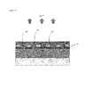
- FIG. 1 is a view schematically illustrating an organic electrochemical device according to a first exemplary embodiment of the present invention.
- the organic electrochemical device according to the first exemplary embodiment comprises a substrate 10, a first electrode 20 provided on the substrate, an intermediate layer 30 provided on the first electrode 20, a second electrode 50 provided on the intermediate layer 30, and a first organic material layer 60, in which at least a part of the first organic material layer 60 is in contact with the second electrode 50 and the intermediate layer 30.
- the substrate 10 may or may not be transparent.
- the thickness of the substrate is not particularly limited as long as the substrate has an appropriate strength allowed in the organic electrochemical device.
- the substrate may be glass, plastic, metal, ceramic, and the like.
- the glass comprise soda glass, borosilicate glass, aluminosilicate glass, aluminoborosilicate glass, silica glass, soda lime glass, and the like.
- the plastic substrate comprise polyester sheet such as polyethylene terephthalate and polyethylene naphthalate, and sheet such as polyphenylene sulfide, polycarbonate, polysulfone, and polyethylidene norbornene.
- the ceramic comprise high-purity alumina, and the like.
- the material for the first electrode 20 is not particularly limited, and metal, conductive oxide, carbon material, conductive polymer and the like may be applied.
- the metal comprise titanium, nickel, platinum, gold, silver, copper, aluminum, tungsten, rhodium, indium, and the like.
- the conductive oxide comprise tin oxide, fluorine-doped tin oxide (FTO), indium oxide, tin-doped indium oxide (ITO), zinc oxide, and the like.
- the carbon material comprise carbon nanotubes, graphene, carbon black, and the like.
- Examples of the conductive polymer comprise PEDOT-PSS, polypyrrole, polyaniline, poly-3,4-ethylenedioxythiophene (poly-EDT), and the like. These materials may be used either alone or in combination thereof.
- the first electrode 20 may be coated on the substrate by a deposition method.
- the first electrode may be formed by depositing a conductive material such as metal, conductive oxide, carbon material, and conductive polymer on the substrate 10 by physical vapor deposition such as thermal metal evaporation, electron beam evaporation, RF sputtering, magnetron sputtering, atomic layer deposition, arc vapor deposition, and ion beam assisted deposition, or a chemical vapor deposition process such as chemical vapor deposition (CVD), metal organic chemical vapor deposition (MOCVD), and plasma-enhanced chemical vapor deposition (PECVD).
- CVD chemical vapor deposition
- MOCVD metal organic chemical vapor deposition
- PECVD plasma-enhanced chemical vapor deposition
- the intermediate layer 30 may be formed on the first electrode 20.
- the intermediate layer may comprise a hole transporting layer, and an insulating layer.
- An organic electrochemical device comprising a hole transporting layer 70 and an insulating layer 40 as the intermediate layer is schematically illustrated in the following FIG. 3 .
- the intermediate layer comprises the hole transporting layer 70, and may additionally comprise the insulating layer 40 between the intermediate layer and the second electrode.
- An organic electrochemical device having the structure is schematically illustrated in the following FIG. 2 .
- the hole transporting layer 70 may comprise a hole transporting material.
- the hole transporting material a material which may transport holes between the first electrode 20 and the first organic material layer 60, and is suitably a material having high hole mobility. Specific examples thereof comprise arylamine-based organic materials, conductive polymers, block copolymers having both conjugated portions and non-conjugated portions and the like, but are not limited thereto.
- examples of the hole transporting material comprise poly(3,4-ethylenediocythiophene) doped with poly(styrenesulfonic acid) (PEDOT:PSS), N, N'-bis(3-methylphenyl)-N,N'-diphenyl-[1,1'-biphenyl]-4,4'-diamine (TPD), and the like, but are not limited thereto.
- PEDOT:PSS poly(3,4-ethylenediocythiophene) doped with poly(styrenesulfonic acid)
- TPD N, N'-bis(3-methylphenyl)-N,N'-diphenyl-[1,1'-biphenyl]-4,4'-diamine
- the insulating layer 40 may be formed by using a material and a method known in the art.
- the intermediate layer 30 may have lower conductivity than those of the first electrode 20 and the second electrode 50.
- the second electrode 50 may be formed on the intermediate layer 30.
- the second electrode 50 may comprise regular patterns or irregular patterns.
- the material for the second electrode 50 is not particularly limited, and metal, conductive oxide, carbon material, conductive polymer, and the like may be applied.
- the metal comprise titanium, nickel, platinum, gold, silver, copper, aluminum, tungsten, rhodium, indium, and the like.
- the conductive oxide comprise tin oxide, fluorine-doped tin oxide (FTO), indium oxide, tin-doped indium oxide (ITO), zinc oxide, and the like.
- the carbon material comprise carbon nanotubes, graphene, carbon black, and the like.
- Examples of the conductive polymer comprise PEDOT-PSS, polypyrrole, polyaniline, poly-EDT, and the like. These materials may be used either alone or in combination thereof.
- the second electrode 50 may be coated on the substrate by a deposition method.
- the second electrode may be formed by depositing a conductive material such as metal, conductive oxide, carbon material, and conductive polymer on the substrate 30 by physical vapor deposition such as thermal metal evaporation, electron beam evaporation, RF sputtering, magnetron sputtering, atomic layer deposition, arc vapor deposition, and ion beam assisted deposition, or a chemical vapor deposition process such as CVD, MOCVD, and PECVD.
- light is absorbed from the side of the glass surface, but in the present invention, light may be absorbed by or emitted into the side of the first organic material layer surface formed on the second electrode by forming the second electrode 50 in regular patterns or irregular patterns.
- both the first electrode 20 and the second electrode 50 may be a metal electrode. Accordingly, it is possible to provide an organic electrochemical device having excellent conductivity.
- the first organic material layer 60 may be formed on the second electrode 50 and the intermediate layer 30. Accordingly, at least a part of the first organic material layer 60 may be in contact with the second electrode and the intermediate layer.
- the surface state of the first organic material layer 60 is not particularly limited.
- the surface state of the first organic material layer 60 may be in the form of a flat surface as illustrated in the following FIG. 2 , and may be in the form of a curved surface as illustrated in the following FIG. 4 .
- the organic electrochemical device according to the present invention may have a structure in which the second electrode 50 is comprised in the first organic material layer 60 as illustrated in the following FIG. 5 .
- the first organic material layer 60 may be an organic photoactive layer.
- the organic photoactive layer may comprise an electron donor material and/or an electron acceptor material.
- the electron donor material it is possible to use a polymer compound which is suitable for the light absorption wavelength range or solar light spectrum, has a strong light absorption, and has excellent electrical properties such as mobility of electric charges.
- the electron donor material may comprise poly(3-hexylthiophene) (P3HT), which is a complex polymer material, but is not limited thereto.
- the electron acceptor material may be fullerene, fullerene derivatives, vasocuproin, semiconductor elements, semiconductor compounds, or combinations thereof, and specifically, may be phenyl C61-butyric acid methyl ester (PC61BM), or phenyl C71-butyric acid methyl ester (PC71BM), but is not limited thereto.
- the electron donor material and the electron acceptor material may form a bulk heterojunction (BHJ).
- the electron donor material and the electron acceptor material may be mixed with each other at a ratio of 1:10 to 10:1 (w/w: mass ratio).
- the electron donor material and the electron acceptor material are mixed, and then may be annealed at 30°C to 300°C for 1 second to 24 hours in order to maximize the characteristics thereof.
- the thickness of the organic photoactive layer may be 10 ⁇ to 10,000 ⁇ , but is not limited thereto.
- the organic photoactive layer may comprise a light emitting material.
- the light emitting material is a material that is capable of emitting light in a visible light region by accepting and recombining holes from the hole transporting layer and electrons from the electron transporting layer, and preferably a material having high quantum efficiency for fluorescence and phosphorescence.
- Specific examples thereof comprise: 8-hydroxy-quinoline-aluminum complex (Alq 3 ); carbazole-based compounds; dimerized styryl compounds; BAlq; 10-hydroxybenzoquinoline-metal compounds; benzoxazole-based, benzthiazole-based, and benzimidazole-based compounds; poly(p-phenylenevinylene)(PPV)-based polymers; spiro compounds; and polyfluorene, rubrene, and the like, but are not limited thereto.
- Alq 3 8-hydroxy-quinoline-aluminum complex
- carbazole-based compounds dimerized styryl compounds
- BAlq 10-hydroxybenzoquinoline-metal compounds
- benzoxazole-based, benzthiazole-based, and benzimidazole-based compounds poly(p-phenylenevinylene)(PPV)-based polymers
- spiro compounds and polyfluorene, rubrene, and the like, but are not limited there
- the organic photoactive layer may be an organic electrochromic layer.
- the organic electrochemical device according to the present invention may be applied to various organic electrochemical devices, such as organic solar cells, organic photodetection elements, organic light emitting elements, and organic electrochromic elements, by controlling a material comprised in the first organic material layer so as to be suitable for the use thereof.
- organic electrochemical devices such as organic solar cells, organic photodetection elements, organic light emitting elements, and organic electrochromic elements
- the organic electrochemical device according to the present invention may additionally comprise a second organic material layer 80 between the intermediate layer 30 and the first organic material layer 60.
- a schematic structure of an organic electrochemical device having the structure is illustrated in the following FIG. 6 .
- the second organic material layer may comprise the aforementioned materials exemplified as the material for the first organic material layer. It is preferred that the first organic material layer comprises a first material, the second organic material layer comprises a second material, and the first material and the second material comprise different materials from each other. Furthermore, it is preferred that the first material and the second material may absorb light in different wavelength ranges from each other and the second material absorbs light having a longer wavelength than the first material, but the present invention is not limited thereto.
- the organic electrochemical device according to the present invention may additionally comprise an electron transporting layer 90 between the first organic material layer 60 and the second electrode 50.
- a schematic structure of an organic electrochemical device having the structure is illustrated in the following FIG. 7 .
- the electron transporting layer 90 may comprise an electron transporting material.
- the electron transporting material is a material which may accept and transfer electrons from the second electrode to the first organic material layer 60, and is suitably a material having high electron mobility. Specific examples thereof comprise aluminum trihydroxyquinoline (Alq3), 2-(4-bipheyl)-5-phenyl-1,3,4-oxadiazole (PBD) which is a 1,3,4-oxadiazole derivative, 1,3,4-tris[(3-phenyl-6-trifluoromethyl)qunoxaline-2-yl]benzene (TPQ) which is a quinoxaline derivative, a triazole derivative, and the like, but are not limited thereto.
- Alq3 aluminum trihydroxyquinoline
- PBD 2-(4-bipheyl)-5-phenyl-1,3,4-oxadiazole
- TPQ 1,3,4-tris[(3-phenyl-6-trifluoromethyl)qunoxaline-2-yl]
- the intermediate layer 30, the insulating layer 40, the hole transporting layer 70, the first organic material layer 60, the second organic material layer 70, the electron transporting layer 90, and the like using various polymer materials by the above-described deposition process, or a solvent process, for example, a method such as spin coating, dip coating, doctor blading, screen printing, inkjet printing, or a thermal transfer method.
- FIG. 8 is a view schematically illustrating an organic electrochemical device according to an eighth exemplary embodiment of the present invention.
- the organic electrochemical device according to the eighth exemplary embodiment comprises a substrate 10, a first organic material layer 60 provided on the substrate, a first electrode 20 provided on the first organic material layer 60, a second electrode 50, and an intermediate layer 30 provided between the first organic material layer 60 and the second electrode 50, in which at least a part of the intermediate layer 30 is in contact with the first electrode 20 and the first organic material layer 60.
- the substrate 10 of the organic electrochemical device according to the eighth exemplary embodiment is transparent.
- the first electrode 20 of the organic electrochemical device according to the eighth exemplary embodiment may comprise regular patterns or irregular patterns.
- light may be absorbed by or emitted into the side of the substrate surface at a lower surface of the first electrode by forming the first electrode 20 in regular patterns or irregular patterns.
- both the first electrode 20 and the second electrode 50 may be a metal electrode. Accordingly, it is possible to provide an organic electrochemical device having excellent conductivity.
- the intermediate layer 30 may comprise a hole transporting layer 70, and an insulating layer 40.
- the intermediate layer 30 comprises the hole transporting layer 70, and may additionally comprise the insulating layer 40 between the intermediate layer 30 and the first electrode 20.
- An organic electrochemical device having the structure is schematically illustrated in the following FIG. 9 .
- the surface state of the hole transporting layer 70 is not particularly limited.
- the surface state of the hole transporting layer 70 may be a flat surface form as illustrated in the following FIG. 9 , and may be an unevenness form as illustrated in the following FIG. 10 .
- the organic electrochemical device according to the eighth exemplary embodiment may additionally comprise a second organic material layer 80 between the intermediate layer 30 and the first organic material layer 60.
- a schematic structure of an organic electrochemical device having the structure is illustrated in the following FIG. 11 .
- the material and forming method for the first electrode 20, the intermediate layer 30, the insulating layer 40, the second electrode 50, the hole transporting layer 70, the first organic material layer 60, the second organic material layer 70, the electron transporting layer 90, and the like are the same as or similar to those described above, and thus the specific description thereof will be omitted.
- the organic electrochemical device according to the present invention may be applied to various organic electrochemical devices such as organic solar cells, organic photodetection elements, organic light emitting elements, and organic electrochromic elements.
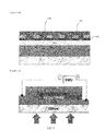
- FIG. 15 An organic solar cell in the related art is schematically illustrated in the following FIG. 15 .
- the organic solar cell according to the present invention is schematically illustrated in the following FIG. 12
- the organic light emitting element according to the present invention is schematically illustrated in the following FIG. 13
- the organic electrochromic element according to the present invention is illustrated in the following FIG. 14 .
- a method for fabricating an organic electrochemical device comprises: forming a first electrode on a substrate; forming an intermediate layer on the first electrode; forming a second electrode on the intermediate layer such that at least a part of the second electrode is in contact with the intermediate layer; and forming a first organic material layer on the intermediate layer.
- a method for fabricating an organic electrochemical device comprises: forming a first organic material layer on a substrate; forming a first electrode on the first organic material layer such that at least a part of the first electrode is in contact with the first organic material layer; forming an intermediate layer on the first organic material layer and the first electrode; and forming a second electrode on the intermediate layer.
- the material and forming method for the first electrode 20, the intermediate layer 30, the insulating layer 40, the second electrode 50, the hole transporting layer 70, the first organic material layer 60, the second organic material layer 70, the electron transporting layer 90, and the like are the same as or similar to those described above, and thus the specific description thereof will be omitted.
- the organic electrochemical device may improve power conversion efficiency because an organic active layer may be formed on a second electrode and an intermediate layer.
- the organic electrochemical device according to another exemplary embodiment of the present invention may use metal electrodes as a first electrode and a second electrode, thereby improving conductivity and being implemented at low costs.
- the organic electrochemical device according to yet another exemplary embodiment of the present invention may improve flexibility of the organic electrochemical device by comprising an organic material layer on a second electrode, may reduce loss of light according to the light absorption of an electrode, a hole transporting layer, and the like by directly irradiating light on the organic material layer provided at an upper portion of the second electrode without passing light through a transparent electrode, and may increase the re-absorption rate of light due to reflection of light from a metal electrode.
- the organic electrochemical device according to the present invention may be applied to various organic electrochemical devices such as organic solar cells, organic photodetection elements, organic light emitting elements, and organic electrochromic elements.
Landscapes
- Physics & Mathematics (AREA)
- Electromagnetism (AREA)
- Optics & Photonics (AREA)
- Nonlinear Science (AREA)
- General Physics & Mathematics (AREA)
- Engineering & Computer Science (AREA)
- Manufacturing & Machinery (AREA)
- Photovoltaic Devices (AREA)
- Electroluminescent Light Sources (AREA)
- Battery Electrode And Active Subsutance (AREA)
Abstract
Description
- The present specification relates to an organic electrochemical device and a fabrication method thereof.
- Crystalline silicon solar cells have been widely known as a device for directly converting light energy into electric energy. The crystalline silicon solar cells are used as an independent power source, and a power source for use in a vehicle. The crystalline silicon solar cells are usually made of silicon single crystals or amorphous silicon. However, enormous amounts of energy is required to produce silicon single crystals or amorphous silicon, and in order to recover energy consumed for fabricating the solar cells, the solar cells needs to generate electric power continuously for almost as long as a ten-year period.
- Meanwhile, in recent a few years, various forms of solar cells using organic molecules have been developed as a new form of a solar cell in which the technical possibility thereof has been rapidly improved. Existing organic solar cells developed until now are still at the beginning stages in energy conversion efficiency, service life, and the like. Presently, since the optical and electric stability of the organic molecules are not at a satisfactory level, the organic solar cell is one of the development fields of solar cells which have been widely studied even until now in order to improve the performances thereof.
- Existing organic solar cells developed until now are very vulnerable to temperature, solar light, a high wavelength system, and the like and have many problems in energy conversion efficiency. Thus, those problems are obstacle factors to the development of solar cells using organic molecules, and particularly, because energy conversion efficiency of solar cells using organic materials is lower than that of the existing silicon solar cells, and the like and the solar cells have many limitations in use thereof, it is difficult to expand the use fields thereof.
- As illustrated in the following
FIG. 15 , an organic solar cell in the related art comprises an indium tin oxide (ITO) electrode provided on a glass substrate, a poly(3,4-ethylenedioxythiophene):poly(styrene sulfonate) (PEDOT/PSS) layer provided on the ITO electrode, an organic active layer provided on the PEDOT/PSS layer and the glass substrate, and an aluminum electrode provided on the organic active layer. - The present invention has been made in an effort to provide an organic electrochemical device having excellent power conversion efficiency, and a fabrication method thereof.
- The present invention provides an organic electrochemical device comprising:
- a substrate;
- a first electrode provided on the substrate;
- an intermediate layer provided on the first electrode;
- a second electrode provided on the intermediate layer; and
- a first organic material layer,
- in which at least a part of the first organic material layer is in contact with the second electrode and the intermediate layer.
- Further, the present invention provides an organic electrochemical device comprising:
- a transparent substrate;
- a first organic material layer provided on the transparent substrate;
- a first electrode provided on the first organic material layer;
- a second electrode; and
- an intermediate layer provided between the first organic material layer and the second electrode,
- in which at least a part of the intermediate layer is in contact with the first electrode and the first organic material layer.
- In addition, the present invention provides a method for fabricating an organic electrochemical device, the method comprising:
- forming a first electrode on a substrate;
- forming an intermediate layer on the first electrode;
- forming a second electrode on the intermediate layer such that at least a part of the second electrode is in contact with the intermediate layer; and
- forming a first organic material layer on the intermediate layer.
- Furthermore, the present invention provides a method for fabricating an organic electrochemical device, the method comprising:
- forming a first organic material layer on a transparent substrate;
- forming a first electrode on the first organic material layer such that at least a part of the first electrode is in contact with the first organic material layer;
- forming an intermediate layer on the first organic material layer and the first electrode; and
- forming a second electrode on the intermediate layer.
- The organic electrochemical device according to an exemplary embodiment of the present invention may improve power conversion efficiency because an organic active layer may be formed on a second electrode and an intermediate layer. Further, the organic electrochemical device according to another exemplary embodiment of the present invention may use metal electrodes as a first electrode and a second electrode, thereby improving conductivity and being implemented at low costs.
- In addition, the organic electrochemical device according to yet another exemplary embodiment of the present invention may improve flexibility of the organic electrochemical device by comprising an organic material layer on a second electrode, may reduce loss of light according to the light absorption of an electrode, a hole transporting layer, and the like by directly irradiating light on the organic material layer provided at an upper portion of the second electrode without passing light through a transparent electrode, and may increase a re-absorption rate of light due to reflection of light from a metal electrode. The organic electrochemical device according to the present invention may be applied to various organic electrochemical devices such as organic solar cells, organic photodetection elements, organic light emitting elements, and organic electrochromic elements.
-
-
FIG. 1 is a view schematically illustrating an organic electrochemical device according to a first exemplary embodiment of the present invention. -
FIG. 2 is a view schematically illustrating an organic electrochemical device according to a second exemplary embodiment of the present invention. -
FIG. 3 is a view schematically illustrating an organic electrochemical device according to a third exemplary embodiment of the present invention. -
FIG. 4 is a view schematically illustrating an organic electrochemical device according to a fourth exemplary embodiment of the present invention. -
FIG. 5 is a view schematically illustrating an organic electrochemical device according to a fifth exemplary embodiment of the present invention. -
FIG. 6 is a view schematically illustrating an organic electrochemical device according to a sixth exemplary embodiment of the present invention. -
FIG. 7 is a view schematically illustrating an organic electrochemical device according to a seventh exemplary embodiment of the present invention. -
FIG. 8 is a view schematically illustrating an organic electrochemical device according to an eighth exemplary embodiment of the present invention. -
FIG. 9 is a view schematically illustrating an organic electrochemical device according to a ninth exemplary embodiment of the present invention. -
FIG. 10 is a view schematically illustrating an organic electrochemical device according to a tenth exemplary embodiment of the present invention. -
FIG. 11 is a view schematically illustrating an organic electrochemical device according to an eleventh exemplary embodiment of the present invention. -
FIG. 12 is a view schematically illustrating an organic solar cell according to a twelfth exemplary embodiment of the present invention. -
FIG. 13 is a view schematically illustrating an organic light emitting element according to a thirteenth exemplary embodiment of the present invention. -
FIG. 14 is a view schematically illustrating an organic electrochromic element according to a fourteenth exemplary embodiment of the present invention. -
FIG. 15 is a view schematically illustrating an organic solar cell in the related art. -
- 10:
- Substrate
- 20:
- First electrode
- 30:
- Intermediate layer
- 40:
- Insulating layer
- 50:
- Second electrode
- 60:
- First organic material layer
- 70:
- Hole transporting layer
- 80:
- Second organic material layer
- 90:
- Electron transporting layer
- 100:
- Ion storing layer
- 110:
- Ion conductor/Electrolyte
- 120:
- Electrochromic layer
- Hereinafter, preferred exemplary embodiments of the present invention will be described in detail with reference to the accompanying drawings.
-
FIG. 1 is a view schematically illustrating an organic electrochemical device according to a first exemplary embodiment of the present invention. The organic electrochemical device according to the first exemplary embodiment comprises asubstrate 10, afirst electrode 20 provided on the substrate, anintermediate layer 30 provided on thefirst electrode 20, asecond electrode 50 provided on theintermediate layer 30, and a firstorganic material layer 60, in which at least a part of the firstorganic material layer 60 is in contact with thesecond electrode 50 and theintermediate layer 30. - The
substrate 10 may or may not be transparent. The thickness of the substrate is not particularly limited as long as the substrate has an appropriate strength allowed in the organic electrochemical device. The substrate may be glass, plastic, metal, ceramic, and the like. Examples of the glass comprise soda glass, borosilicate glass, aluminosilicate glass, aluminoborosilicate glass, silica glass, soda lime glass, and the like. Examples of the plastic substrate comprise polyester sheet such as polyethylene terephthalate and polyethylene naphthalate, and sheet such as polyphenylene sulfide, polycarbonate, polysulfone, and polyethylidene norbornene. Examples of the ceramic comprise high-purity alumina, and the like. - The material for the
first electrode 20 is not particularly limited, and metal, conductive oxide, carbon material, conductive polymer and the like may be applied. Examples of the metal comprise titanium, nickel, platinum, gold, silver, copper, aluminum, tungsten, rhodium, indium, and the like. Examples of the conductive oxide comprise tin oxide, fluorine-doped tin oxide (FTO), indium oxide, tin-doped indium oxide (ITO), zinc oxide, and the like. Examples of the carbon material comprise carbon nanotubes, graphene, carbon black, and the like. Examples of the conductive polymer comprise PEDOT-PSS, polypyrrole, polyaniline, poly-3,4-ethylenedioxythiophene (poly-EDT), and the like. These materials may be used either alone or in combination thereof. - The
first electrode 20 may be coated on the substrate by a deposition method. The first electrode may be formed by depositing a conductive material such as metal, conductive oxide, carbon material, and conductive polymer on thesubstrate 10 by physical vapor deposition such as thermal metal evaporation, electron beam evaporation, RF sputtering, magnetron sputtering, atomic layer deposition, arc vapor deposition, and ion beam assisted deposition, or a chemical vapor deposition process such as chemical vapor deposition (CVD), metal organic chemical vapor deposition (MOCVD), and plasma-enhanced chemical vapor deposition (PECVD). - The
intermediate layer 30 may be formed on thefirst electrode 20. The intermediate layer may comprise a hole transporting layer, and an insulating layer. An organic electrochemical device comprising ahole transporting layer 70 and an insulatinglayer 40 as the intermediate layer is schematically illustrated in the followingFIG. 3 . - Furthermore, the intermediate layer comprises the
hole transporting layer 70, and may additionally comprise the insulatinglayer 40 between the intermediate layer and the second electrode. An organic electrochemical device having the structure is schematically illustrated in the followingFIG. 2 . - The
hole transporting layer 70 may comprise a hole transporting material. The hole transporting material a material which may transport holes between thefirst electrode 20 and the firstorganic material layer 60, and is suitably a material having high hole mobility. Specific examples thereof comprise arylamine-based organic materials, conductive polymers, block copolymers having both conjugated portions and non-conjugated portions and the like, but are not limited thereto. - More specifically, examples of the hole transporting material comprise poly(3,4-ethylenediocythiophene) doped with poly(styrenesulfonic acid) (PEDOT:PSS), N, N'-bis(3-methylphenyl)-N,N'-diphenyl-[1,1'-biphenyl]-4,4'-diamine (TPD), and the like, but are not limited thereto.
- The insulating
layer 40 may be formed by using a material and a method known in the art. - The
intermediate layer 30 may have lower conductivity than those of thefirst electrode 20 and thesecond electrode 50. - The
second electrode 50 may be formed on theintermediate layer 30. Thesecond electrode 50 may comprise regular patterns or irregular patterns. - The material for the
second electrode 50 is not particularly limited, and metal, conductive oxide, carbon material, conductive polymer, and the like may be applied. Examples of the metal comprise titanium, nickel, platinum, gold, silver, copper, aluminum, tungsten, rhodium, indium, and the like. Examples of the conductive oxide comprise tin oxide, fluorine-doped tin oxide (FTO), indium oxide, tin-doped indium oxide (ITO), zinc oxide, and the like. Examples of the carbon material comprise carbon nanotubes, graphene, carbon black, and the like. Examples of the conductive polymer comprise PEDOT-PSS, polypyrrole, polyaniline, poly-EDT, and the like. These materials may be used either alone or in combination thereof. - The
second electrode 50 may be coated on the substrate by a deposition method. The second electrode may be formed by depositing a conductive material such as metal, conductive oxide, carbon material, and conductive polymer on thesubstrate 30 by physical vapor deposition such as thermal metal evaporation, electron beam evaporation, RF sputtering, magnetron sputtering, atomic layer deposition, arc vapor deposition, and ion beam assisted deposition, or a chemical vapor deposition process such as CVD, MOCVD, and PECVD. - In particular, in the structure of the organic solar cell in the related art as illustrated in the following
FIG. 15 , light is absorbed from the side of the glass surface, but in the present invention, light may be absorbed by or emitted into the side of the first organic material layer surface formed on the second electrode by forming thesecond electrode 50 in regular patterns or irregular patterns. - Further, in the present invention, both the
first electrode 20 and thesecond electrode 50 may be a metal electrode. Accordingly, it is possible to provide an organic electrochemical device having excellent conductivity. - The first
organic material layer 60 may be formed on thesecond electrode 50 and theintermediate layer 30. Accordingly, at least a part of the firstorganic material layer 60 may be in contact with the second electrode and the intermediate layer. - The surface state of the first
organic material layer 60 is not particularly limited. The surface state of the firstorganic material layer 60 may be in the form of a flat surface as illustrated in the followingFIG. 2 , and may be in the form of a curved surface as illustrated in the followingFIG. 4 . - In addition, the organic electrochemical device according to the present invention may have a structure in which the
second electrode 50 is comprised in the firstorganic material layer 60 as illustrated in the followingFIG. 5 . - The first
organic material layer 60 may be an organic photoactive layer. - When the organic electrochemical device is applied to an organic solar cell, the organic photoactive layer may comprise an electron donor material and/or an electron acceptor material.
- As the electron donor material, it is possible to use a polymer compound which is suitable for the light absorption wavelength range or solar light spectrum, has a strong light absorption, and has excellent electrical properties such as mobility of electric charges. The electron donor material may comprise poly(3-hexylthiophene) (P3HT), which is a complex polymer material, but is not limited thereto.
- The electron acceptor material may be fullerene, fullerene derivatives, vasocuproin, semiconductor elements, semiconductor compounds, or combinations thereof, and specifically, may be phenyl C61-butyric acid methyl ester (PC61BM), or phenyl C71-butyric acid methyl ester (PC71BM), but is not limited thereto.
- In the organic photoactive layer, the electron donor material and the electron acceptor material may form a bulk heterojunction (BHJ). The electron donor material and the electron acceptor material may be mixed with each other at a ratio of 1:10 to 10:1 (w/w: mass ratio). The electron donor material and the electron acceptor material are mixed, and then may be annealed at 30°C to 300°C for 1 second to 24 hours in order to maximize the characteristics thereof.
- The thickness of the organic photoactive layer may be 10Å to 10,000 Å, but is not limited thereto.
- When the organic electrochemical device is applied to an organic light emitting element, the organic photoactive layer may comprise a light emitting material. The light emitting material is a material that is capable of emitting light in a visible light region by accepting and recombining holes from the hole transporting layer and electrons from the electron transporting layer, and preferably a material having high quantum efficiency for fluorescence and phosphorescence. Specific examples thereof comprise: 8-hydroxy-quinoline-aluminum complex (Alq3); carbazole-based compounds; dimerized styryl compounds; BAlq; 10-hydroxybenzoquinoline-metal compounds; benzoxazole-based, benzthiazole-based, and benzimidazole-based compounds; poly(p-phenylenevinylene)(PPV)-based polymers; spiro compounds; and polyfluorene, rubrene, and the like, but are not limited thereto.
- When the organic electrochemical device is applied to an organic electrochromic element, the organic photoactive layer may be an organic electrochromic layer.
- As described above, the organic electrochemical device according to the present invention may be applied to various organic electrochemical devices, such as organic solar cells, organic photodetection elements, organic light emitting elements, and organic electrochromic elements, by controlling a material comprised in the first organic material layer so as to be suitable for the use thereof.
- The organic electrochemical device according to the present invention may additionally comprise a second
organic material layer 80 between theintermediate layer 30 and the firstorganic material layer 60. A schematic structure of an organic electrochemical device having the structure is illustrated in the followingFIG. 6 . - The second organic material layer may comprise the aforementioned materials exemplified as the material for the first organic material layer. It is preferred that the first organic material layer comprises a first material, the second organic material layer comprises a second material, and the first material and the second material comprise different materials from each other. Furthermore, it is preferred that the first material and the second material may absorb light in different wavelength ranges from each other and the second material absorbs light having a longer wavelength than the first material, but the present invention is not limited thereto.
- The organic electrochemical device according to the present invention may additionally comprise an
electron transporting layer 90 between the firstorganic material layer 60 and thesecond electrode 50. A schematic structure of an organic electrochemical device having the structure is illustrated in the followingFIG. 7 . - The
electron transporting layer 90 may comprise an electron transporting material. The electron transporting material is a material which may accept and transfer electrons from the second electrode to the firstorganic material layer 60, and is suitably a material having high electron mobility. Specific examples thereof comprise aluminum trihydroxyquinoline (Alq3), 2-(4-bipheyl)-5-phenyl-1,3,4-oxadiazole (PBD) which is a 1,3,4-oxadiazole derivative, 1,3,4-tris[(3-phenyl-6-trifluoromethyl)qunoxaline-2-yl]benzene (TPQ) which is a quinoxaline derivative, a triazole derivative, and the like, but are not limited thereto. - It is possible to fabricate the
intermediate layer 30, the insulatinglayer 40, thehole transporting layer 70, the firstorganic material layer 60, the secondorganic material layer 70, theelectron transporting layer 90, and the like using various polymer materials by the above-described deposition process, or a solvent process, for example, a method such as spin coating, dip coating, doctor blading, screen printing, inkjet printing, or a thermal transfer method. -
FIG. 8 is a view schematically illustrating an organic electrochemical device according to an eighth exemplary embodiment of the present invention. The organic electrochemical device according to the eighth exemplary embodiment comprises asubstrate 10, a firstorganic material layer 60 provided on the substrate, afirst electrode 20 provided on the firstorganic material layer 60, asecond electrode 50, and anintermediate layer 30 provided between the firstorganic material layer 60 and thesecond electrode 50, in which at least a part of theintermediate layer 30 is in contact with thefirst electrode 20 and the firstorganic material layer 60. - It is preferred that the
substrate 10 of the organic electrochemical device according to the eighth exemplary embodiment is transparent. - The
first electrode 20 of the organic electrochemical device according to the eighth exemplary embodiment may comprise regular patterns or irregular patterns. In the present invention, light may be absorbed by or emitted into the side of the substrate surface at a lower surface of the first electrode by forming thefirst electrode 20 in regular patterns or irregular patterns. - Further, in the present invention, both the
first electrode 20 and thesecond electrode 50 may be a metal electrode. Accordingly, it is possible to provide an organic electrochemical device having excellent conductivity. - In the organic electrochemical device according to the eighth exemplary embodiment, the
intermediate layer 30 may comprise ahole transporting layer 70, and an insulatinglayer 40. In addition, theintermediate layer 30 comprises thehole transporting layer 70, and may additionally comprise the insulatinglayer 40 between theintermediate layer 30 and thefirst electrode 20. An organic electrochemical device having the structure is schematically illustrated in the followingFIG. 9 . - The surface state of the
hole transporting layer 70 is not particularly limited. The surface state of thehole transporting layer 70 may be a flat surface form as illustrated in the followingFIG. 9 , and may be an unevenness form as illustrated in the followingFIG. 10 . - The organic electrochemical device according to the eighth exemplary embodiment may additionally comprise a second
organic material layer 80 between theintermediate layer 30 and the firstorganic material layer 60. A schematic structure of an organic electrochemical device having the structure is illustrated in the followingFIG. 11 . - In the organic electrochemical device according to the eighth exemplary embodiment, the material and forming method for the
first electrode 20, theintermediate layer 30, the insulatinglayer 40, thesecond electrode 50, thehole transporting layer 70, the firstorganic material layer 60, the secondorganic material layer 70, theelectron transporting layer 90, and the like are the same as or similar to those described above, and thus the specific description thereof will be omitted. - The organic electrochemical device according to the present invention may be applied to various organic electrochemical devices such as organic solar cells, organic photodetection elements, organic light emitting elements, and organic electrochromic elements.
- An organic solar cell in the related art is schematically illustrated in the following
FIG. 15 . In addition, the organic solar cell according to the present invention is schematically illustrated in the followingFIG. 12 , the organic light emitting element according to the present invention is schematically illustrated in the followingFIG. 13 , and the organic electrochromic element according to the present invention is illustrated in the followingFIG. 14 . - Furthermore, a method for fabricating an organic electrochemical device according to an exemplary embodiment of the present invention comprises: forming a first electrode on a substrate; forming an intermediate layer on the first electrode; forming a second electrode on the intermediate layer such that at least a part of the second electrode is in contact with the intermediate layer; and forming a first organic material layer on the intermediate layer.
- Further, a method for fabricating an organic electrochemical device according to another exemplary embodiment of the present invention comprises: forming a first organic material layer on a substrate; forming a first electrode on the first organic material layer such that at least a part of the first electrode is in contact with the first organic material layer; forming an intermediate layer on the first organic material layer and the first electrode; and forming a second electrode on the intermediate layer.
- In the method for fabricating an organic electrochemical device according to the present invention, the material and forming method for the
first electrode 20, theintermediate layer 30, the insulatinglayer 40, thesecond electrode 50, thehole transporting layer 70, the firstorganic material layer 60, the secondorganic material layer 70, theelectron transporting layer 90, and the like are the same as or similar to those described above, and thus the specific description thereof will be omitted. - The organic electrochemical device according to an exemplary embodiment of the present invention may improve power conversion efficiency because an organic active layer may be formed on a second electrode and an intermediate layer. In addition, the organic electrochemical device according to another exemplary embodiment of the present invention may use metal electrodes as a first electrode and a second electrode, thereby improving conductivity and being implemented at low costs.
- Furthermore, the organic electrochemical device according to yet another exemplary embodiment of the present invention may improve flexibility of the organic electrochemical device by comprising an organic material layer on a second electrode, may reduce loss of light according to the light absorption of an electrode, a hole transporting layer, and the like by directly irradiating light on the organic material layer provided at an upper portion of the second electrode without passing light through a transparent electrode, and may increase the re-absorption rate of light due to reflection of light from a metal electrode. The organic electrochemical device according to the present invention may be applied to various organic electrochemical devices such as organic solar cells, organic photodetection elements, organic light emitting elements, and organic electrochromic elements.
Claims (27)
- An organic electrochemical device comprising:a substrate;a first electrode provided on the substrate;an intermediate layer provided on the first electrode;a second electrode provided on the intermediate layer; anda first organic material layer,wherein at least a part of the first organic material layer is in contact with the second electrode and the intermediate layer.
- The organic electrochemical device of claim 1, wherein the intermediate layer comprises a hole transporting layer.
- The organic electrochemical device of claim 2, wherein the intermediate layer comprises an insulating layer.
- The organic electrochemical device of claim 2, further comprising:an insulating layer provided between the intermediate layer and the second electrode.
- The organic electrochemical device of claim 1, wherein both the first electrode and the second electrode are a metal electrode.
- The organic electrochemical device of claim 1, wherein the first organic material layer is an organic photoactive layer.
- The organic electrochemical device of claim 1, further comprising:a second organic material layer provided between the intermediate layer and the first organic material layer.
- The organic electrochemical device of claim 7, wherein the first organic material layer comprises a first material, the second organic material layer comprises a second material, and
the first material and the second material are different materials from each other. - The organic electrochemical device of claim 8, wherein the first material and the second material absorb light in different wavelength ranges from each other.
- The organic electrochemical device of claim 9, wherein the second material absorbs light having a longer wavelength than the first material.
- The organic electrochemical device of claim 1, wherein the second electrode comprises regular patterns or irregular patterns.
- The organic electrochemical device of claim 1, further comprising:an electron transporting layer provided on the second electrode.
- An organic electrochemical device comprising:a substrate;a first organic material layer provided on the substrate;a first electrode provided on the first organic material layer;a second electrode; andan intermediate layer provided between the first organic material layer and the second electrode,wherein at least a part of the intermediate layer is in contact with the first electrode and the first organic material layer.
- The organic electrochemical device of claim 13, wherein the intermediate layer comprises a hole transporting layer.
- The organic electrochemical device of claim 14, wherein the intermediate layer comprises an insulating layer.
- The organic electrochemical device of claim 14, further comprising:an insulating layer provided between the first electrode and the intermediate layer.
- The organic electrochemical device of claim 13, wherein both the first electrode and the second electrode are a metal electrode.
- The organic electrochemical device of claim 13, wherein the first organic material layer is an organic photoactive layer.
- The organic electrochemical device of claim 13, further comprising:a second organic material layer provided between the intermediate layer and the first organic material layer.
- The organic electrochemical device of claim 19, wherein the first organic material layer comprises a first material, the second organic material layer comprises a second material, and
the first material and the second material are different materials from each other. - The organic electrochemical device of claim 20, wherein the first material and the second material absorb light in different wavelength ranges from each other.
- The organic electrochemical device of claim 21, wherein the second material absorbs light having a longer wavelength than the first material.
- The organic electrochemical device of claim 13, wherein the second electrode comprises regular patterns or irregular patterns.
- The organic electrochemical device of claim 13, further comprising:an electron transporting layer provided between the first organic material layer and the first electrode.
- The organic electrochemical device of any one of claims 1 to 24, wherein the organic electrochemical device is selected from the group consisting of organic solar cells, organic photodetection elements, and organic electrochromic elements.
- A method for fabricating an organic electrochemical device, the method comprising:forming a first electrode on a substrate;forming an intermediate layer on the first electrode;forming a second electrode on the intermediate layer such that at least a part of the second electrode is in contact with the intermediate layer; andforming a first organic material layer on the intermediate layer.
- A method for fabricating an organic electrochemical device, the method comprising:forming a first organic material layer on a substrate;forming a first electrode on the first organic material layer such that at least a part of the first electrode is in contact with the first organic material layer;forming an intermediate layer on the first organic material layer and the first electrode; andforming a second electrode on the intermediate layer.
Applications Claiming Priority (2)
| Application Number | Priority Date | Filing Date | Title |
|---|---|---|---|
| US201261644536P | 2012-05-09 | 2012-05-09 | |
| PCT/KR2013/004111 WO2013169047A1 (en) | 2012-05-09 | 2013-05-09 | Organic electrochemical device, and method for manufacturing same |
Publications (2)
| Publication Number | Publication Date |
|---|---|
| EP2833427A1 true EP2833427A1 (en) | 2015-02-04 |
| EP2833427A4 EP2833427A4 (en) | 2016-02-24 |
Family
ID=49551000
Family Applications (1)
| Application Number | Title | Priority Date | Filing Date |
|---|---|---|---|
| EP13787335.2A Withdrawn EP2833427A4 (en) | 2012-05-09 | 2013-05-09 | ORGANIC ELECTROCHEMICAL DEVICE AND METHOD FOR PRODUCING THE SAME |
Country Status (7)
| Country | Link |
|---|---|
| US (1) | US10326091B2 (en) |
| EP (1) | EP2833427A4 (en) |
| JP (1) | JP5999258B2 (en) |
| KR (1) | KR101412896B1 (en) |
| CN (1) | CN104272486A (en) |
| IN (1) | IN2014DN09305A (en) |
| WO (1) | WO2013169047A1 (en) |
Families Citing this family (13)
| Publication number | Priority date | Publication date | Assignee | Title |
|---|---|---|---|---|
| CA2930038A1 (en) * | 2013-11-15 | 2015-05-21 | The Governing Council Of The University Of Toronto | Polyfullerenes useful as electrodes for high power supercapacitors |
| JP6425921B2 (en) * | 2014-06-12 | 2018-11-21 | 株式会社ジャパンディスプレイ | Image display device |
| KR102167932B1 (en) * | 2015-03-10 | 2020-10-21 | 한국전자통신연구원 | Complex display device |
| GB201517629D0 (en) * | 2015-10-06 | 2015-11-18 | Isis Innovation | Device architecture |
| KR101972636B1 (en) | 2016-01-14 | 2019-08-26 | 단국대학교 산학협력단 | Organic device for X-ray detect and method of manufacturing the same |
| KR102067546B1 (en) | 2017-02-24 | 2020-01-17 | 단국대학교 산학협력단 | Organic device for X-ray detect and method of manufacturing the same |
| EP3389096A1 (en) * | 2017-04-13 | 2018-10-17 | Nederlandse Organisatie voor toegepast- natuurwetenschappelijk onderzoek TNO | Photo-voltaic element and method of manufacturing the same |
| CN111123610A (en) * | 2018-11-01 | 2020-05-08 | 苏州苏大维格科技集团股份有限公司 | Electrochromic display panel and electronic paper |
| KR102380472B1 (en) | 2019-11-07 | 2022-03-30 | 단국대학교 산학협력단 | X-ray Detect and Method of Manufacturing the Same |
| CN111293222B (en) * | 2020-02-25 | 2024-03-22 | 南开大学 | Positive interdigital full back contact perovskite solar cell and preparation method thereof |
| CN111312900A (en) * | 2020-02-25 | 2020-06-19 | 南开大学 | Parallel interdigital full back contact perovskite solar cell and preparation method thereof |
| CN111312901A (en) * | 2020-02-25 | 2020-06-19 | 南开大学 | Stacking interdigital full back contact perovskite solar cell and preparation method thereof |
| CN111599921B (en) * | 2020-04-09 | 2023-07-21 | 南开大学 | Nested full back contact perovskite solar cell and preparation method thereof |
Family Cites Families (36)
| Publication number | Priority date | Publication date | Assignee | Title |
|---|---|---|---|---|
| WO1997016838A1 (en) | 1995-10-31 | 1997-05-09 | Ecole Polytechnique Federale De Lausanne | A battery of photovoltaic cells and process for manufacturing the same |
| JPH11354279A (en) * | 1998-06-09 | 1999-12-24 | Idemitsu Kosan Co Ltd | Organic electroluminescence device |
| TWI232595B (en) * | 1999-06-04 | 2005-05-11 | Semiconductor Energy Lab | Electroluminescence display device and electronic device |
| JP2002117985A (en) * | 2000-08-03 | 2002-04-19 | Semiconductor Energy Lab Co Ltd | Light emitting device |
| JP3944348B2 (en) * | 2000-09-25 | 2007-07-11 | 株式会社東芝 | Organic light emitting device |
| JP2002203676A (en) | 2000-12-27 | 2002-07-19 | Asahi Glass Co Ltd | Organic electroluminescent display device |
| US20040031965A1 (en) * | 2002-08-16 | 2004-02-19 | Forrest Stephen R. | Organic photonic integrated circuit using an organic photodetector and a transparent organic light emitting device |
| JP4074803B2 (en) * | 2002-10-28 | 2008-04-16 | シャープ株式会社 | Method for manufacturing photoelectric conversion element |
| CN100508238C (en) * | 2004-05-11 | 2009-07-01 | Lg化学株式会社 | Organic electronic device |
| US7375370B2 (en) | 2004-08-05 | 2008-05-20 | The Trustees Of Princeton University | Stacked organic photosensitive devices |
| US7326955B2 (en) | 2004-08-05 | 2008-02-05 | The Trustees Of Princeton University | Stacked organic photosensitive devices |
| JP4765281B2 (en) * | 2004-08-23 | 2011-09-07 | ソニー株式会社 | Photoelectric conversion element and manufacturing method thereof |
| GB0523163D0 (en) | 2005-11-14 | 2005-12-21 | Suisse Electronique Microtech | Patterning of conductive layers with underlying compressible spacer layer or spacer layer stack |
| TW200802903A (en) * | 2006-02-16 | 2008-01-01 | Solexant Corp | Nanoparticle sensitized nanostructured solar cells |
| JP5303828B2 (en) * | 2006-09-14 | 2013-10-02 | 大日本印刷株式会社 | Organic thin film solar cell |
| DE102006051101A1 (en) | 2006-10-25 | 2008-04-30 | Osram Opto Semiconductors Gmbh | Organic light-emitting diode (OLED) with structured baking electrode and method for producing an OLED with structured baking electrode |
| US20090032107A1 (en) | 2007-08-03 | 2009-02-05 | Korea Institute Of Machinery & Materials | Organic solar cell using conductive polymer transparent electrode and fabricating method thereof |
| TWI405340B (en) | 2007-08-31 | 2013-08-11 | Nexpower Technology Corp | Thin film solar cell and manufacturing method thereof |
| US7888593B2 (en) * | 2007-09-05 | 2011-02-15 | Northwestern University | TFB:TPDSi2 interfacial layer usable in organic photovoltaic cells |
| JP2009088045A (en) | 2007-09-28 | 2009-04-23 | Hitachi Ltd | Photoelectric conversion element and manufacturing method thereof |
| DE102007046502A1 (en) * | 2007-09-28 | 2009-04-16 | Siemens Ag | Organic opto-electronic component with reduced dark current |
| WO2009084078A1 (en) | 2007-12-27 | 2009-07-09 | Pioneer Corporation | Organic semiconductor device, organic solar cell and display panel |
| TWI379427B (en) | 2007-12-31 | 2012-12-11 | Ind Tech Res Inst | Transparent solar cell module |
| KR20090092114A (en) * | 2008-02-26 | 2009-08-31 | 삼성모바일디스플레이주식회사 | Electron injecting layer comprising super acid salt, photovoltaic device including the same and electron injecting layer including the same |
| KR100999377B1 (en) | 2008-06-18 | 2010-12-09 | 한국과학기술원 | Organic based solar cell and manufacturing method thereof |
| KR100937867B1 (en) * | 2008-06-19 | 2010-01-21 | 삼성모바일디스플레이주식회사 | Organic light emitting display device |
| EP2172986B1 (en) | 2008-08-27 | 2013-08-21 | Honeywell International Inc. | Solar cell having hybrid hetero junction structure |
| DE102008045948A1 (en) | 2008-09-04 | 2010-03-11 | Osram Opto Semiconductors Gmbh | Method for producing an organic radiation-emitting component and organic radiation-emitting component |
| CN102341431B (en) * | 2009-03-04 | 2014-04-30 | 思研(Sri)国际顾问与咨询公司 | Encapsulation method and dielectric layer for electromechanical device |
| US20100319765A1 (en) | 2009-06-17 | 2010-12-23 | Korea University Research And Business Foundation | Photovoltaic devices |
| US9581870B2 (en) | 2009-08-13 | 2017-02-28 | 3M Innovative Properties Company | Conducting film or electrode with improved optical and electrical performance for display and lighting devices and solar cells |
| WO2011052565A1 (en) * | 2009-10-30 | 2011-05-05 | 住友化学株式会社 | Organic photoelectric conversion element |
| WO2011112714A2 (en) * | 2010-03-09 | 2011-09-15 | The Regents Of The University Of Michigan | Methods of making organic photovoltaic cells having improved heterojunction morphology |
| JP2011192761A (en) * | 2010-03-12 | 2011-09-29 | Lintec Corp | Organic thin film solar cell device, method for manufacturing the same, and substrate for forming organic thin film solar cell device |
| FR2960703B1 (en) * | 2010-05-28 | 2012-05-18 | Commissariat Energie Atomique | OPTOELECTRONIC DEVICE WITH ELECTRODE ENTERREE |
| GB2482110B (en) * | 2010-07-05 | 2014-08-27 | Cambridge Display Tech Ltd | Lighting elements |
-
2013
- 2013-05-09 IN IN9305DEN2014 patent/IN2014DN09305A/en unknown
- 2013-05-09 US US14/398,651 patent/US10326091B2/en active Active
- 2013-05-09 JP JP2015511369A patent/JP5999258B2/en active Active
- 2013-05-09 EP EP13787335.2A patent/EP2833427A4/en not_active Withdrawn
- 2013-05-09 WO PCT/KR2013/004111 patent/WO2013169047A1/en not_active Ceased
- 2013-05-09 CN CN201380023941.0A patent/CN104272486A/en active Pending
- 2013-05-09 KR KR20130052693A patent/KR101412896B1/en active Active
Also Published As
| Publication number | Publication date |
|---|---|
| KR101412896B1 (en) | 2014-06-26 |
| JP2015525461A (en) | 2015-09-03 |
| KR20130125737A (en) | 2013-11-19 |
| JP5999258B2 (en) | 2016-09-28 |
| CN104272486A (en) | 2015-01-07 |
| US20150123094A1 (en) | 2015-05-07 |
| IN2014DN09305A (en) | 2015-07-10 |
| US10326091B2 (en) | 2019-06-18 |
| EP2833427A4 (en) | 2016-02-24 |
| WO2013169047A1 (en) | 2013-11-14 |
Similar Documents
| Publication | Publication Date | Title |
|---|---|---|
| US10326091B2 (en) | Organic electrochemical device, and method for manufacturing same | |
| Lian et al. | Polymer modification on the NiO x hole transport layer boosts open-circuit voltage to 1.19 V for perovskite solar cells | |
| CN101208815B (en) | Organic photoactive component | |
| KR101776533B1 (en) | Preparing method for bonded type perovskite solar cell | |
| ES2950269T3 (en) | Single junction organic photovoltaic devices having high open circuit voltages and applications thereof | |
| KR101557587B1 (en) | Organic solar cell and manufacturing the same | |
| CN107001599A (en) | Polymers and organic solar cells containing them | |
| US20110041905A1 (en) | Organic solar cell and method for forming the same | |
| EP3012279B1 (en) | Copolymer and organic solar cell comprising same | |
| CN106663739A (en) | Solar cell and manufacturing method thereof | |
| CN104733614A (en) | Organic thin-film solar cell based on dual mixed active layers and preparation method thereof | |
| US9269916B2 (en) | Organic thin-film solar cell module and sub-module | |
| KR101862920B1 (en) | Compound of perovskite structure, solar cell and thin film transister using the same | |
| CN102201536B (en) | Organic thin-film solar battery and fabrication method thereof | |
| KR20180035057A (en) | Organic photovoltaics and method for manufacturing the same | |
| KR101563048B1 (en) | Active layer, organic photovoltaic cell comprising the same and manufacturing method thereof | |
| EP1756869A1 (en) | Photovoltaic device with trimetaspheres | |
| CN104766926A (en) | Organic thin film solar cell based on three-layer donor layer and its preparation method | |
| TWI599065B (en) | Organic electrochemical device and fabrication method thereof | |
| US20120118366A1 (en) | Double-sided light-collecting organic solar cell | |
| KR101923625B1 (en) | Method for manufacturing organic solar cell and organic solar cell manufactured by the same | |
| KR20180000474A (en) | Semitransparent organic photovoltaics and method for manufacturing the same | |
| KR102907949B1 (en) | Heat transfer interlayer for improved photovoltaic performance and device operational stability of perovskite solar cells | |
| CN104795500A (en) | Organic thin-film solar cell using bulk heterojunctions as linking layers and production method of solar cell | |
| KR102924403B1 (en) | A zwitterionic cathode interlayer for improved photovoltaic performance and device operational stability of perovskite solar cells |
Legal Events
| Date | Code | Title | Description |
|---|---|---|---|
| PUAI | Public reference made under article 153(3) epc to a published international application that has entered the european phase |
Free format text: ORIGINAL CODE: 0009012 |
|
| 17P | Request for examination filed |
Effective date: 20141031 |
|
| AK | Designated contracting states |
Kind code of ref document: A1 Designated state(s): AL AT BE BG CH CY CZ DE DK EE ES FI FR GB GR HR HU IE IS IT LI LT LU LV MC MK MT NL NO PL PT RO RS SE SI SK SM TR |
|
| AX | Request for extension of the european patent |
Extension state: BA ME |
|
| DAX | Request for extension of the european patent (deleted) | ||
| RA4 | Supplementary search report drawn up and despatched (corrected) |
Effective date: 20160125 |
|
| RIC1 | Information provided on ipc code assigned before grant |
Ipc: H01L 51/10 20060101AFI20160119BHEP |
|
| 17Q | First examination report despatched |
Effective date: 20180726 |
|
| STAA | Information on the status of an ep patent application or granted ep patent |
Free format text: STATUS: THE APPLICATION IS DEEMED TO BE WITHDRAWN |
|
| 18D | Application deemed to be withdrawn |
Effective date: 20181206 |