EP2833403A2 - Header for electronic cooler - Google Patents
Header for electronic cooler Download PDFInfo
- Publication number
- EP2833403A2 EP2833403A2 EP20140178071 EP14178071A EP2833403A2 EP 2833403 A2 EP2833403 A2 EP 2833403A2 EP 20140178071 EP20140178071 EP 20140178071 EP 14178071 A EP14178071 A EP 14178071A EP 2833403 A2 EP2833403 A2 EP 2833403A2
- Authority
- EP
- European Patent Office
- Prior art keywords
- header
- return
- supply
- portions
- fluid
- Prior art date
- Legal status (The legal status is an assumption and is not a legal conclusion. Google has not performed a legal analysis and makes no representation as to the accuracy of the status listed.)
- Granted
Links
Images



Classifications
-
- H—ELECTRICITY
- H05—ELECTRIC TECHNIQUES NOT OTHERWISE PROVIDED FOR
- H05K—PRINTED CIRCUITS; CASINGS OR CONSTRUCTIONAL DETAILS OF ELECTRIC APPARATUS; MANUFACTURE OF ASSEMBLAGES OF ELECTRICAL COMPONENTS
- H05K1/00—Printed circuits
- H05K1/02—Details
- H05K1/0201—Thermal arrangements, e.g. for cooling, heating or preventing overheating
- H05K1/0203—Cooling of mounted components
-
- F—MECHANICAL ENGINEERING; LIGHTING; HEATING; WEAPONS; BLASTING
- F28—HEAT EXCHANGE IN GENERAL
- F28D—HEAT-EXCHANGE APPARATUS, NOT PROVIDED FOR IN ANOTHER SUBCLASS, IN WHICH THE HEAT-EXCHANGE MEDIA DO NOT COME INTO DIRECT CONTACT
- F28D15/00—Heat-exchange apparatus with the intermediate heat-transfer medium in closed tubes passing into or through the conduit walls ; Heat-exchange apparatus employing intermediate heat-transfer medium or bodies
-
- H—ELECTRICITY
- H05—ELECTRIC TECHNIQUES NOT OTHERWISE PROVIDED FOR
- H05K—PRINTED CIRCUITS; CASINGS OR CONSTRUCTIONAL DETAILS OF ELECTRIC APPARATUS; MANUFACTURE OF ASSEMBLAGES OF ELECTRICAL COMPONENTS
- H05K7/00—Constructional details common to different types of electric apparatus
- H05K7/20—Modifications to facilitate cooling, ventilating, or heating
- H05K7/20009—Modifications to facilitate cooling, ventilating, or heating using a gaseous coolant in electronic enclosures
-
- H—ELECTRICITY
- H05—ELECTRIC TECHNIQUES NOT OTHERWISE PROVIDED FOR
- H05K—PRINTED CIRCUITS; CASINGS OR CONSTRUCTIONAL DETAILS OF ELECTRIC APPARATUS; MANUFACTURE OF ASSEMBLAGES OF ELECTRICAL COMPONENTS
- H05K7/00—Constructional details common to different types of electric apparatus
- H05K7/20—Modifications to facilitate cooling, ventilating, or heating
- H05K7/20218—Modifications to facilitate cooling, ventilating, or heating using a liquid coolant without phase change in electronic enclosures
-
- H—ELECTRICITY
- H10—SEMICONDUCTOR DEVICES; ELECTRIC SOLID-STATE DEVICES NOT OTHERWISE PROVIDED FOR
- H10W—GENERIC PACKAGES, INTERCONNECTIONS, CONNECTORS OR OTHER CONSTRUCTIONAL DETAILS OF DEVICES COVERED BY CLASS H10
- H10W40/00—Arrangements for thermal protection or thermal control
- H10W40/40—Arrangements for thermal protection or thermal control involving heat exchange by flowing fluids
- H10W40/47—Arrangements for thermal protection or thermal control involving heat exchange by flowing fluids by flowing liquids, e.g. forced water cooling
Definitions
- This application relates to a header for supplying cooling fluid to electronic components and for returning the cooling fluid.
- the electronics are being packed in plural arrays.
- the cooling fluid must be provided to the several electronics components in an efficient manner.
- a fluid cooler packet for a plurality of electronic components has a plurality of individual cooling circuits for receiving a supply of cooling fluid from a supply header and delivering that cooling fluid to an associated electronic component.
- the plurality of cooling circuits each includes a return passage for receiving a return fluid after having cooled the associated electronic component, and returns the return fluid to a return header.
- a volume of the supply header decreases in a downstream direction as it passes over the plurality of individual cooling circuits.
- a volume of the return header increases as it moves in a downstream direction over the plurality of individual cooling circuits.
- Figure 1 shows an electronic assembly 20.
- the assembly includes an electronic component 22 that may be extremely small and on the order of one millimeter by one millimeter as an example. Of course, this size is merely an example.
- the electronic component 22 may be a computer chip or other electronic element.
- the component is shown schematically controlling a system 15.
- the electronic component 22 is shown schematically connected to system 15 by connector pins 28.
- An area 26 may generate more heat than an area 24.
- Figure 2A shows an array 40 that provides a fluid cooler packet.
- the array 40 incorporates and cools a large number of the assemblies 20, such as shown in Figure 1 .
- other numbers would come within the scope of this disclosure.
- a supply port 42 and a discharge or return port 44 are shown.
- a cooling packet or circuit 141 associated with one of the assemblies 20 is shown in an exploded view.
- a supply 17 supplies cooling fluid into the supply port 42, and a downstream destination 15 receives return fluid from the return port 44.
- a heat exchanger HE may be between the destination 15, and source 17 such that the cooling fluid is recirculated in a closed loop.
- a silicone layer 46 is positioned adjacent the assembly 20.
- An impingement channel layer 50 has a plurality of channels 251 extending generally parallel to each other.
- the layer 50 has a higher density central area 47, with a higher density of channels 251, and a lower density outer area 49 with a lower density of channels 251.
- the lower density area 49 is associated with cooling the area 24 of component 22 while the area 47 is positioned to cool the higher heat area 26.
- An orifice layer 52 includes a plurality of holes 51 in a higher density area 331, and other holes 153 in a lower density area 332.
- a small slot layer 54 provides a number of supply and return slots 23 and has area 53 with a high density of slots 23 and area 55 of a lower density of slots 23. As can be appreciated, these areas are also associated with the area 26 and the area 24 on component 22, respectively.
- the small slot layer 54 has a channel 754 which communicates with a plurality of the slots 23 in the upper surface. It should be understood that spaced into the plane of this Figure, there would be other channels, which are maintained separate from channel 754, and alternate ones of the channels provide supply and return flow passages, as will be better described below.
- a large slot layer 56 has slots 111 that communicate the slots 23 in the small slot layer 56 into a plurality of channels 59 in an outer channel layer 58.
- a porting layer 60 has openings 61, 62, 63 and 64. As can be seen, an opening 64 is associated with one channel 59. Ribs 159 within the layer 58 separate the channels 59, such that other openings 61, 63 and 64 are each associated with distinct channels 59.
- the slots 111 communicate with an elongated channel 756. Again, separate channels would be spaced into the plane of this Figure, and would also provide separate supply and return passages. In general, the slots and channels of the layer 54 and layer 56 extend perpendicular to each other.
- a separator layer 66/69 has walls which will separate the flow from the openings 61 and 64 into a channel or passage 68 and the flow from ports 62 and 63 into a channel or passage 70.
- a header portion 72 has a closure wall 74 blocking flow from the channel 68 into a passage 76, but allowing flow from the channel 70 into the passage 76. Downstream of the header 72, there will be another header, which provides the reverse structure, and will communicate the channel 68 into another passage similar to passage 76.
- a portion of the passage 76 communicates with a space 75 that would be above the wall 74, and channel or passage 68.
- this provides a "nested" arrangement for the header which more efficiently uses the overall space.
- Figure 2E shows the assembly of the various layers on to the assembly 20. If the channel 68 is a supply channel and the channel 70 is a return channel, then fluid would be supplied into the channel 68, pass through the opening 64 and 61 into channels 59 in the layer 58, and then through associated slots 111 in the layer 56, through slots 23 in the layer 54, holes 51/153 in layer 52, and into a channel 251 in layer 50.
- the flow downstream of the orifices 51/153 in the layer 52 then impacts upon the electronic component 20 cooling it.
- the fluid passes along the channel 251 until moving back outwardly through other holes 51/153 in the orifice layer 54 that may be associated with slots 23 in the small slot layer 54, and associated with a slot 111 moving into a channels 159 that is associated with a return passage.
- the fluid then passes through an opening 62/63 in porting layer 60 and into passage 76.
- Figure 3A shows the spaces within the layers of Figures 2B and 2C , rather than the structure of the layers.
- Figure 3 is a "reverse" model from the structure illustrated in the earlier figures and shows the shape and size of the flow passages, rather than the structure that forms the flow passages.
- the lines separating areas in Figure 3 would actually include structure, such as the walls and the layers as shown in the earlier figures.
- Figure 3A shows the combination of the channel 70 and passage 76 communicating with an opening 63 to in turn communicate with a channel 59.
- Another channel 59 is shown as being separated by a line 200.
- the line 200 will actually be a structural wall in the cooling circuit as formed.
- An area 140 would be an opening into one of the slots 111, and a portion 156 would be formed by the slots 111 within the body of the layer 56.
- Portions 226 are formed by the slots in the small slot layer 54.
- Pins 225 are formed by the holes in the orifice layer 52.
- the portions 222 are the actual impingement channels 51 within the impingement channel layer 50.
- the disclosure has focused largely on cooling a single assembly 20.
- the overall array of embodiment 40 may include a plurality of such assemblies.
- Figure 3B shows the impingement of the fluid coming through one orifice 225 into an impingement channel 222.
- Figure 3B is also a "reverse" model showing the flow passages rather than structure. This flow then impacts upon the component to be cooled, flows along a channel, and then moves upwardly through an adjacent orifice 225 and communicates back through a return passage 226, which may be defined by the channel 754 in the small slot layer 54.
- Figure 3C shows the adjacent passages 226 formed by the channels 756 communicating through slots 111 to passages 854 which are formed by the channels 754 in the large slot layer 54. The slots 111 will then communicate these passages 754 along supply and return paths, as can be appreciated.
- Figure 3C is also a "reverse" model.
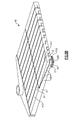
- Figure 4 shows a header structure for the array 40. As shown in Figure 4 , a supply header S and a return header R are positioned at opposed ends of an array 340. This is not the "nested" embodiment as mentioned above with regard to Figure 2B , but rather an alternative.
- the supply header has a highest volume 501 decreasing through steps 502, and eventually reaching a smallest point 509.
- this header embodiment 340 will ensure that the pressure is maintained as desired along the entire flow path.
- the supply header portions 611 decrease in size, and hence volume, in a downstream direction moving from the supply port 42 toward the return port 44.
- the return header steps increase along each of the parallel return header portions 613.
- the array 340 is a 10 x 10 array cooling 100 electronic components 22. Each step along each of the parallel supply and return header portions 611 and 613 would change by 10% from the prior step.
- the change would not be 10%. However, in some embodiments, the change is generally equal for each step. As an example, if there were four steps, the change might be 25% on each step, in one embodiment.
- assemblies 20 are formed into columns and rows, with the rows each being associated with one of the parallel supply header portions 611, and one of the parallel return header portions 613. Each step along each of the portions 611/613 is associated with one of the columns across the rows.
- Figure 5A shows a header embodiment 140.
- Header embodiment 140 more efficiently utilizes a space (see 65 in Figure 2B , as an example) which is above the steps of the header embodiment 340, and results in a more compact overall array 40.
- This nested embodiment is what is illustrated in Figure 2B .
- the supply header S has its portions shown to the bottom right hand side of Figure 5A which actually communicate the cooling fluid and decrease in size as shown at 68. These are also nested return header portions 151, 152, etc. above the supply header portions.
- the supply header communicates to cool an assembly through a cooling circuit and as shown at 211.
- There are decreasing channel steps 68 which are provided by the structure shown at 142, 146, 147, etc. in Figure 5A .
- a portion 210 of the return header R also communicates with a cooling circuit 42, and would for example be the channel 76 as shown in Figure 2B .
- the header embodiments illustrated in this invention provide improved pressure regulation along the path of both the supply and return fluids. It should be understood that all of the flow passages illustrated in this disclosure can be formed by silicon layering techniques.
Landscapes
- Engineering & Computer Science (AREA)
- Microelectronics & Electronic Packaging (AREA)
- Physics & Mathematics (AREA)
- Thermal Sciences (AREA)
- Mechanical Engineering (AREA)
- General Engineering & Computer Science (AREA)
- Cooling Or The Like Of Semiconductors Or Solid State Devices (AREA)
- Cooling Or The Like Of Electrical Apparatus (AREA)
Abstract
Description
- This application relates to a header for supplying cooling fluid to electronic components and for returning the cooling fluid.
- Electronics are becoming utilized in more and more applications. The size of the electronic components is continuously being reduced. There are now any number of electronic chips that are sized one millimeter by one millimeter, and even smaller.
- As the applications controlled and performed by the electronics have increased, the heat generated by the electronics has also increased. The historic ways of dissipating heat, such as heat fins, may no longer always be adequate. Thus, it becomes important to provide cooling fluid in an efficient manner to the very small electronic components.
- In addition, the electronics are being packed in plural arrays. The cooling fluid must be provided to the several electronics components in an efficient manner.
- A fluid cooler packet for a plurality of electronic components has a plurality of individual cooling circuits for receiving a supply of cooling fluid from a supply header and delivering that cooling fluid to an associated electronic component. The plurality of cooling circuits each includes a return passage for receiving a return fluid after having cooled the associated electronic component, and returns the return fluid to a return header. A volume of the supply header decreases in a downstream direction as it passes over the plurality of individual cooling circuits. A volume of the return header increases as it moves in a downstream direction over the plurality of individual cooling circuits. An electronic component array is also disclosed.
- These and other features may be best understood from the following drawings and specification.
-
-
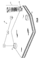
Figure 1 shows an electronic component. -
Figure 2A shows an array including a plurality of theFigure 1 components. -
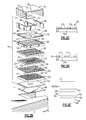
Figure 2B shows a cooling circuit for cooling one of the electronic components within the array ofFigure 2A . -
Figure 2C shows a detail of one layer. -
Figure 2D shows a detail of another layer. -
Figure 2E shows a sandwich assembly of layers shown inFigure 2B . -
Figure 3A shows the overall flow passage associated with one cooling circuit. -
Figure 3B shows a portion of the flow path. -
Figure 3C shows another portion of the flow path. -
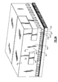
Figure 4 shows a header for communicating all of the separate cooling circuits together. -
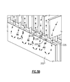
Figure 5A shows an alternative header. -
Figure 5B shows a detail of theFigure 5A header. -
Figure 5C shows a benefit of theFigure 5A header. -
Figure 5D shows another embodiment. -
Figure 1 shows anelectronic assembly 20. The assembly includes anelectronic component 22 that may be extremely small and on the order of one millimeter by one millimeter as an example. Of course, this size is merely an example. - The
electronic component 22 may be a computer chip or other electronic element. The component is shown schematically controlling asystem 15. Theelectronic component 22 is shown schematically connected tosystem 15 byconnector pins 28. Anarea 26 may generate more heat than anarea 24. - Thus,
Figure 2A shows anarray 40 that provides a fluid cooler packet. Thearray 40 incorporates and cools a large number of theassemblies 20, such as shown inFigure 1 . In one embodiment, there may be a 10 by 10 array of theFigure 1 assemblies 20 within thearray 40. Of course, other numbers would come within the scope of this disclosure. - A
supply port 42 and a discharge orreturn port 44 are shown. A cooling packet orcircuit 141 associated with one of theassemblies 20 is shown in an exploded view. As shown, asupply 17 supplies cooling fluid into thesupply port 42, and adownstream destination 15 receives return fluid from thereturn port 44. As shown schematically, a heat exchanger HE may be between thedestination 15, andsource 17 such that the cooling fluid is recirculated in a closed loop. - As shown in
Figure 2B , asilicone layer 46 is positioned adjacent theassembly 20. - An
impingement channel layer 50 has a plurality ofchannels 251 extending generally parallel to each other. - As can be seen, the
layer 50 has a higher densitycentral area 47, with a higher density ofchannels 251, and a lower densityouter area 49 with a lower density ofchannels 251. Thelower density area 49 is associated with cooling thearea 24 ofcomponent 22 while thearea 47 is positioned to cool thehigher heat area 26. - An
orifice layer 52 includes a plurality ofholes 51 in ahigher density area 331, andother holes 153 in alower density area 332. - A
small slot layer 54 provides a number of supply andreturn slots 23 and hasarea 53 with a high density ofslots 23 andarea 55 of a lower density ofslots 23. As can be appreciated, these areas are also associated with thearea 26 and thearea 24 oncomponent 22, respectively. - As shown somewhat schematically in
Figure 2C , thesmall slot layer 54 has achannel 754 which communicates with a plurality of theslots 23 in the upper surface. It should be understood that spaced into the plane of this Figure, there would be other channels, which are maintained separate fromchannel 754, and alternate ones of the channels provide supply and return flow passages, as will be better described below. - A
large slot layer 56 hasslots 111 that communicate theslots 23 in thesmall slot layer 56 into a plurality ofchannels 59 in anouter channel layer 58. Aporting layer 60 hasopenings opening 64 is associated with onechannel 59.Ribs 159 within thelayer 58 separate thechannels 59, such thatother openings distinct channels 59. - As shown schematically in
Figure 2D , theslots 111 communicate with anelongated channel 756. Again, separate channels would be spaced into the plane of this Figure, and would also provide separate supply and return passages. In general, the slots and channels of thelayer 54 andlayer 56 extend perpendicular to each other. - A
separator layer 66/69 has walls which will separate the flow from theopenings passage 68 and the flow fromports passage 70. Aheader portion 72 has aclosure wall 74 blocking flow from thechannel 68 into apassage 76, but allowing flow from thechannel 70 into thepassage 76. Downstream of theheader 72, there will be another header, which provides the reverse structure, and will communicate thechannel 68 into another passage similar topassage 76. - As can be appreciated from
Figure 2B , a portion of thepassage 76 communicates with aspace 75 that would be above thewall 74, and channel orpassage 68. As will be disclosed below, with regard to the overall header, this provides a "nested" arrangement for the header which more efficiently uses the overall space. -
Figure 2E shows the assembly of the various layers on to theassembly 20. If thechannel 68 is a supply channel and thechannel 70 is a return channel, then fluid would be supplied into thechannel 68, pass through theopening channels 59 in thelayer 58, and then through associatedslots 111 in thelayer 56, throughslots 23 in thelayer 54, holes 51/153 inlayer 52, and into achannel 251 inlayer 50. - The flow downstream of the
orifices 51/153 in thelayer 52 then impacts upon theelectronic component 20 cooling it. The fluid passes along thechannel 251 until moving back outwardly throughother holes 51/153 in theorifice layer 54 that may be associated withslots 23 in thesmall slot layer 54, and associated with aslot 111 moving into achannels 159 that is associated with a return passage. - The fluid then passes through an
opening 62/63 in portinglayer 60 and intopassage 76. -
Figure 3A shows the spaces within the layers ofFigures 2B and 2C , rather than the structure of the layers.Figure 3 is a "reverse" model from the structure illustrated in the earlier figures and shows the shape and size of the flow passages, rather than the structure that forms the flow passages. The lines separating areas inFigure 3 would actually include structure, such as the walls and the layers as shown in the earlier figures. -
Figure 3A shows the combination of thechannel 70 andpassage 76 communicating with anopening 63 to in turn communicate with achannel 59. Anotherchannel 59 is shown as being separated by aline 200. As mentioned above, theline 200 will actually be a structural wall in the cooling circuit as formed. - An
area 140 would be an opening into one of theslots 111, and aportion 156 would be formed by theslots 111 within the body of thelayer 56.Portions 226 are formed by the slots in thesmall slot layer 54.Pins 225 are formed by the holes in theorifice layer 52. Theportions 222 are theactual impingement channels 51 within theimpingement channel layer 50. - To this point, the disclosure has focused largely on cooling a
single assembly 20. However, as mentioned above, the overall array ofembodiment 40 may include a plurality of such assemblies. -
Figure 3B shows the impingement of the fluid coming through oneorifice 225 into animpingement channel 222.Figure 3B is also a "reverse" model showing the flow passages rather than structure. This flow then impacts upon the component to be cooled, flows along a channel, and then moves upwardly through anadjacent orifice 225 and communicates back through areturn passage 226, which may be defined by thechannel 754 in thesmall slot layer 54. -
Figure 3C shows theadjacent passages 226 formed by thechannels 756 communicating throughslots 111 topassages 854 which are formed by thechannels 754 in thelarge slot layer 54. Theslots 111 will then communicate thesepassages 754 along supply and return paths, as can be appreciated.Figure 3C is also a "reverse" model. -
Figure 4 shows a header structure for thearray 40. As shown inFigure 4 , a supply header S and a return header R are positioned at opposed ends of anarray 340. This is not the "nested" embodiment as mentioned above with regard toFigure 2B , but rather an alternative. - Any other number of other arrangements can be utilized to communicate between the header and the component to be cooled.
- There would be a greater amount of supply fluid at an upstream end of the
supply port 42, and a smaller amount of return fluid at that most upstream point. As the supply header moves toward a downstream end, the volume of the supply fluid would decrease, while the volume of return fluid would increase. Thus, inembodiment 340, there is a "stepped" sizing to the headers, such that the return header has asmallest volume point 609, increasing throughpoint - On the other hand, the supply header has a
highest volume 501 decreasing throughsteps 502, and eventually reaching asmallest point 509. By sizing the header flow volumes to increase or decrease as the volume could be handled by also increases or decreases, thisheader embodiment 340 will ensure that the pressure is maintained as desired along the entire flow path. - There are also a plurality of parallel
supply header portions 611 and parallelreturn header portions 613. Thesupply header portions 611 decrease in size, and hence volume, in a downstream direction moving from thesupply port 42 toward thereturn port 44. As illustrated there are a plurality ofassemblies 20 associated with each of the steps, such that the parallelsupply header portions 611 decrease in a stepped manner with eachassembly 20 moving in a downstream direction. Similarly, the return header steps increase along each of the parallelreturn header portions 613. In one embodiment, thearray 340 is a 10 x 10 array cooling 100electronic components 22. Each step along each of the parallel supply and returnheader portions - Of course, if there were a number other than 10 of the steps, the change would not be 10%. However, in some embodiments, the change is generally equal for each step. As an example, if there were four steps, the change might be 25% on each step, in one embodiment.
- It could be said that the
assemblies 20 are formed into columns and rows, with the rows each being associated with one of the parallelsupply header portions 611, and one of the parallelreturn header portions 613. Each step along each of theportions 611/613 is associated with one of the columns across the rows. -
Figure 5A shows aheader embodiment 140.Header embodiment 140 more efficiently utilizes a space (see 65 inFigure 2B , as an example) which is above the steps of theheader embodiment 340, and results in a more compactoverall array 40. This nested embodiment is what is illustrated inFigure 2B . As can be appreciated, the supply header S has its portions shown to the bottom right hand side ofFigure 5A which actually communicate the cooling fluid and decrease in size as shown at 68. These are also nestedreturn header portions - Thus, the unused space beyond the stepped header portions of the
Figure 4 embodiment 340 are now utilized to provide some of the flow volume. - As seen in
Figure 5B , which is again a reverse model, the supply header communicates to cool an assembly through a cooling circuit and as shown at 211. There are decreasingchannel steps 68, which are provided by the structure shown at 142, 146, 147, etc. inFigure 5A . However, there is a nestedportion 206 of the return header R which extends outwardly, or on a reverse face of supply headers facing away from the component andcooling circuits 42. This nested portion is formed for example by the area orspace 75 as shown inFigure 2B . Aportion 210 of the return header R also communicates with acooling circuit 42, and would for example be thechannel 76 as shown inFigure 2B . - Again, there would be associated rows and columns, and associated parallel
supply header portions 413, and associated parallelreturn header portions 411. - As shown in
Figures 5A and5B , there is abreakpoint 911 between an upper surface of thesupply header portions 413, and an upper surface of thereturn header portions 411. In the first half of the "steps," there would be a nested portion on the supply header above the return header. In a second half, the nested portion are as illustrated inFigures 5A and5B , as being part of the return header, and being outwardly of the supply header step portions. This switch in the headers that have the nested portion is necessary, as the nested portion must be able to communicate with the portion actually supplying the fluid to the components in the supply header, and able to communicate back into the return header from those components. Thus, it is only some of the plurality of cooling circuits which have the nested portions on the return header and the nested portions on the supply header. - With the
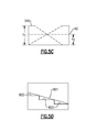
embodiment 40 as illustrated inFigures 5A and5B , there is a reduction in height as is illustrated inFigure 5C . Theembodiment 340 would require a height h1 due to the unused space. Theembodiment 40 however would have a much smaller height h2, while maintaining the same flow vs pressure drop performance, due to the nested combination. - The header embodiments illustrated in this invention provide improved pressure regulation along the path of both the supply and return fluids. It should be understood that all of the flow passages illustrated in this disclosure can be formed by silicon layering techniques.
- Further, while the increase and decrease in the headers is shown in a step fashion, in embodiments, they may generally be more ramped, and formed along a single slope. Thus, as shown in
Figure 5D , rather than the steps shown at 800, one embodiment would actually extend along a slope shown at 801. - Although an embodiment of this invention has been disclosed, a worker of ordinary skill in this art would recognize that certain modifications would come within the scope of this disclosure. For that reason, the following claims should be studied to determine the true scope and content of this disclosure.
Claims (10)
- A fluid cooler packet (141) for a plurality of electronic components (22) comprising:a plurality of individual cooling circuits for receiving a supply of cooling fluid from a supply header (S) and delivering that cooling fluid to an associated electronic component (22), said plurality of cooling circuits each including a return passage for receiving a return fluid after having cooled the associated electronic component (22), and returning the return fluid to a return header (R); anda volume of the supply header (S) decreasing in a downstream direction as it passes over the plurality of individual cooling circuits, and a volume of the return header (R) increasing as it moves in a downstream direction over the plurality of individual cooling circuits.
- The packet as set forth in claim 1, wherein said plurality of individual cooling circuits are assembled in an array of rows and columns, and there are a plurality of parallel supply header portions (611;413) associated with each of said rows, and a plurality of parallel return header portions (613;411) associated with each of said rows, with a downstream direction being defined across said plurality of columns.
- The packet as set forth in claim 2, wherein said plurality of parallel supply header portions (611;413) decrease in steps across each of said plurality of individual cooling circuits, and said plurality of parallel return header portions (613;411) increasing in steps across each of said plurality of individual cooling circuits.
- The packet as set forth in claim 3, wherein a supply port (42) communicates with said supply header (S) at one end of said fluid cooler, and a return port positioned at an opposed end relative to the supply port communicates with said return header (R).
- The packet as set forth in claim 3 or 4, wherein said parallel supply header portions have nested portions which are positioned outwardly of a face of said parallel return header portions spaced away from at least some of the individual cooling circuits, with a volume of said nested portions of said parallel supply header portions decreasing as said volume of said return header parallel portions increases in a downstream direction, and said parallel return header portions have nested portions which are positioned outwardly of a face of said parallel supply header portions spaced away from at least some of the individual cooling circuits, with a volume of said nested portions of said parallel return header portions increasing as said volume of said supply header parallel portions decreases in a downstream direction.
- The packet as set forth in any of claims 1 to 4, wherein said return header (R) has a nested portion associated with a face of said supply header facing away from at least some of the plurality of cooling circuits, and said nested portion of said return header increasing in volume as the volume of said supply header decreases in a downstream direction, and said supply header having a nested portion outwardly of a face of said return header facing away from at least some of the plurality of individual cooling circuits, with said nested portion of said supply header decreasing in volume as said return header increases in volume along a downstream direction.
- The packet as set forth in claims 4, 5 or 6, wherein walls isolate said nested portions, with said walls being outwardly of return and supply channel portions to separate return and supply fluid flows.
- The packet as set forth in any preceding claim, wherein the individual cooling circuits include an impingement channel layer (50) for directing fluid against an electronic component, and communicating that fluid back through into said return header (R).
- The packet as set forth in claim 8, wherein an orifice layer (52) is positioned outwardly of the impingement channel layer (50), with said orifice layer (52) having a plurality of holes (51), with sets of said holes communicating with a return channel portion, and other of said holes (51) communicating with a supply channel portion, with said return and supply channels communicating back into said return and supply headers (R,S), respectively.
- An electronic component array comprising:a plurality of electronic components; anda fluid cooler packet as set forth in any preceding claim, each individual cooling circuit delivering cooling fluid to an associated one of said plurality of electronic components.
Applications Claiming Priority (1)
| Application Number | Priority Date | Filing Date | Title |
|---|---|---|---|
| US13/956,420 US20150034280A1 (en) | 2013-08-01 | 2013-08-01 | Header for electronic cooler |
Publications (3)
| Publication Number | Publication Date |
|---|---|
| EP2833403A2 true EP2833403A2 (en) | 2015-02-04 |
| EP2833403A3 EP2833403A3 (en) | 2015-06-17 |
| EP2833403B1 EP2833403B1 (en) | 2017-05-24 |
Family
ID=51352389
Family Applications (1)
| Application Number | Title | Priority Date | Filing Date |
|---|---|---|---|
| EP14178071.8A Active EP2833403B1 (en) | 2013-08-01 | 2014-07-22 | Header for electronic cooler |
Country Status (3)
| Country | Link |
|---|---|
| US (1) | US20150034280A1 (en) |
| EP (1) | EP2833403B1 (en) |
| JP (1) | JP6364272B2 (en) |
Families Citing this family (4)
| Publication number | Priority date | Publication date | Assignee | Title |
|---|---|---|---|---|
| US9477275B2 (en) * | 2013-01-18 | 2016-10-25 | Intel Corporation | Thermal management solution for circuit products |
| CN114830041A (en) * | 2019-10-25 | 2022-07-29 | 进化添加剂解决方案股份有限公司 | Cooling apparatus and method for additive manufacturing |
| JP7856556B2 (en) * | 2022-12-19 | 2026-05-11 | 株式会社フジクラ | Cold Plate |
| CN117497497B (en) * | 2023-12-29 | 2024-05-10 | 国网浙江省电力有限公司电力科学研究院 | A liquid cooling and heat dissipation packaging structure for a power module |
Family Cites Families (21)
| Publication number | Priority date | Publication date | Assignee | Title |
|---|---|---|---|---|
| US5050036A (en) * | 1989-10-24 | 1991-09-17 | Amdahl Corporation | Liquid cooled integrated circuit assembly |
| US5016707A (en) * | 1989-12-28 | 1991-05-21 | Sundstrand Corporation | Multi-pass crossflow jet impingement heat exchanger |
| JPH07114250B2 (en) * | 1990-04-27 | 1995-12-06 | インターナショナル・ビジネス・マシーンズ・コーポレイション | Heat transfer system |
| DE19514545A1 (en) * | 1995-04-20 | 1996-10-24 | Daimler Benz Ag | Micro-cooling device for multiple microelectronic components |
| KR20040088554A (en) * | 2002-02-26 | 2004-10-16 | 미크로스 매뉴팩처링 인코포레이티드 | Capillary evaporator |
| US7000684B2 (en) * | 2002-11-01 | 2006-02-21 | Cooligy, Inc. | Method and apparatus for efficient vertical fluid delivery for cooling a heat producing device |
| US7414843B2 (en) * | 2004-03-10 | 2008-08-19 | Intel Corporation | Method and apparatus for a layered thermal management arrangement |
| US7204299B2 (en) * | 2004-11-09 | 2007-04-17 | Delphi Technologies, Inc. | Cooling assembly with sucessively contracting and expanding coolant flow |
| US7353859B2 (en) * | 2004-11-24 | 2008-04-08 | General Electric Company | Heat sink with microchannel cooling for power devices |
| JP5137379B2 (en) * | 2005-11-14 | 2013-02-06 | インターナショナル・ビジネス・マシーンズ・コーポレーション | Collision cooler |
| US7762314B2 (en) * | 2007-04-24 | 2010-07-27 | International Business Machines Corporation | Cooling apparatus, cooled electronic module and methods of fabrication employing a manifold structure with interleaved coolant inlet and outlet passageways |
| US7884468B2 (en) * | 2007-07-30 | 2011-02-08 | GM Global Technology Operations LLC | Cooling systems for power semiconductor devices |
| TWI423403B (en) * | 2007-09-17 | 2014-01-11 | 萬國商業機器公司 | Integrated circuit stack |
| US20090211977A1 (en) * | 2008-02-27 | 2009-08-27 | Oregon State University | Through-plate microchannel transfer devices |
| US7921828B2 (en) * | 2008-03-20 | 2011-04-12 | GM Global Technology Operations LLC | Modulating flow through an exhaust gas recirculation cooler to maintain gas flow velocities conducive to reducing deposit build-ups |
| US8418751B2 (en) * | 2008-05-13 | 2013-04-16 | International Business Machines Corporation | Stacked and redundant chip coolers |
| WO2009153735A1 (en) * | 2008-06-18 | 2009-12-23 | Brusa Elektronik Ag | Cooling system, in particular for electronic structural units |
| US8403030B2 (en) * | 2009-04-30 | 2013-03-26 | Lg Chem, Ltd. | Cooling manifold |
| JP5488599B2 (en) * | 2009-06-22 | 2014-05-14 | 株式会社明電舎 | heatsink |
| US9455213B2 (en) * | 2009-08-28 | 2016-09-27 | Raytheon Company | Architecture for gas cooled parallel microchannel array cooler |
| US20120012299A1 (en) * | 2010-07-16 | 2012-01-19 | Industrial Idea Partners, Inc. | Proportional Micro-Valve With Thermal Feedback |
-
2013
- 2013-08-01 US US13/956,420 patent/US20150034280A1/en not_active Abandoned
-
2014
- 2014-07-22 EP EP14178071.8A patent/EP2833403B1/en active Active
- 2014-07-30 JP JP2014154377A patent/JP6364272B2/en active Active
Non-Patent Citations (1)
| Title |
|---|
| None |
Also Published As
| Publication number | Publication date |
|---|---|
| JP2015032831A (en) | 2015-02-16 |
| EP2833403A3 (en) | 2015-06-17 |
| US20150034280A1 (en) | 2015-02-05 |
| JP6364272B2 (en) | 2018-07-25 |
| EP2833403B1 (en) | 2017-05-24 |
Similar Documents
| Publication | Publication Date | Title |
|---|---|---|
| JP5803963B2 (en) | Cooler | |
| US12100643B2 (en) | Thermal management of electronics using co-located microjet nozzles and electronic elements | |
| US10288330B2 (en) | Microchannel evaporators with reduced pressure drop | |
| EP3884520B1 (en) | Cooling system | |
| US7110260B2 (en) | Method and apparatus for cooling heat-generating structure | |
| TWI405531B (en) | Heat sink, two-phase microchannel heat sink, electronic device, method for providing heat sink, and method for dissipating at least one electronic device | |
| KR101624523B1 (en) | Heat dissipation device and semiconductor device | |
| EP2833403B1 (en) | Header for electronic cooler | |
| CN111052360A (en) | Heat sink | |
| US9642287B2 (en) | Cooling plate and data processing system provided with cooling plates | |
| KR20040050910A (en) | High heat flux single-phase heat exchanger | |
| CN115621646A (en) | Battery and method for manufacturing battery | |
| EP4443494A1 (en) | Heat dissipating lid, chip package structure, and device interconnection system | |
| US20190080984A1 (en) | Liquid-cooled type cooling device | |
| CN120379229B (en) | Heat sinks and electronic devices | |
| US9455213B2 (en) | Architecture for gas cooled parallel microchannel array cooler | |
| EP2830088B1 (en) | Cooling fluid flow passage matrix for electronics cooling | |
| JP7644236B2 (en) | Power Semiconductor Components | |
| JP2015149361A (en) | Cooler | |
| JP7693105B2 (en) | Coolers for cooling power electronics equipment | |
| US20210341231A1 (en) | Flow distributor for cooling an electrical component, a semiconductor module comprising such a flow distributor, and method of manufacturing the same | |
| EP2878011B1 (en) | Heat exchanging apparatus and method for transferring heat | |
| JP2005268305A (en) | heatsink | |
| JP2014183277A (en) | Cooler | |
| KR20260071211A (en) | Implementation of a two-phase cold plate loop having design features to optimize thermofluid performance in a space-constrained computer architecture |
Legal Events
| Date | Code | Title | Description |
|---|---|---|---|
| 17P | Request for examination filed |
Effective date: 20140722 |
|
| AK | Designated contracting states |
Kind code of ref document: A2 Designated state(s): AL AT BE BG CH CY CZ DE DK EE ES FI FR GB GR HR HU IE IS IT LI LT LU LV MC MK MT NL NO PL PT RO RS SE SI SK SM TR |
|
| AX | Request for extension of the european patent |
Extension state: BA ME |
|
| PUAI | Public reference made under article 153(3) epc to a published international application that has entered the european phase |
Free format text: ORIGINAL CODE: 0009012 |
|
| PUAL | Search report despatched |
Free format text: ORIGINAL CODE: 0009013 |
|
| AK | Designated contracting states |
Kind code of ref document: A3 Designated state(s): AL AT BE BG CH CY CZ DE DK EE ES FI FR GB GR HR HU IE IS IT LI LT LU LV MC MK MT NL NO PL PT RO RS SE SI SK SM TR |
|
| AX | Request for extension of the european patent |
Extension state: BA ME |
|
| RIC1 | Information provided on ipc code assigned before grant |
Ipc: F28D 15/00 20060101ALI20150508BHEP Ipc: H01L 23/473 20060101AFI20150508BHEP Ipc: H05K 7/20 20060101ALI20150508BHEP |
|
| R17P | Request for examination filed (corrected) |
Effective date: 20151216 |
|
| RBV | Designated contracting states (corrected) |
Designated state(s): AL AT BE BG CH CY CZ DE DK EE ES FI FR GB GR HR HU IE IS IT LI LT LU LV MC MK MT NL NO PL PT RO RS SE SI SK SM TR |
|
| GRAP | Despatch of communication of intention to grant a patent |
Free format text: ORIGINAL CODE: EPIDOSNIGR1 |
|
| STAA | Information on the status of an ep patent application or granted ep patent |
Free format text: STATUS: GRANT OF PATENT IS INTENDED |
|
| INTG | Intention to grant announced |
Effective date: 20161214 |
|
| GRAS | Grant fee paid |
Free format text: ORIGINAL CODE: EPIDOSNIGR3 |
|
| GRAA | (expected) grant |
Free format text: ORIGINAL CODE: 0009210 |
|
| STAA | Information on the status of an ep patent application or granted ep patent |
Free format text: STATUS: THE PATENT HAS BEEN GRANTED |
|
| AK | Designated contracting states |
Kind code of ref document: B1 Designated state(s): AL AT BE BG CH CY CZ DE DK EE ES FI FR GB GR HR HU IE IS IT LI LT LU LV MC MK MT NL NO PL PT RO RS SE SI SK SM TR |
|
| REG | Reference to a national code |
Ref country code: GB Ref legal event code: FG4D |
|
| REG | Reference to a national code |
Ref country code: CH Ref legal event code: EP |
|
| REG | Reference to a national code |
Ref country code: IE Ref legal event code: FG4D |
|
| REG | Reference to a national code |
Ref country code: AT Ref legal event code: REF Ref document number: 896386 Country of ref document: AT Kind code of ref document: T Effective date: 20170615 |
|
| REG | Reference to a national code |
Ref country code: FR Ref legal event code: PLFP Year of fee payment: 4 |
|
| REG | Reference to a national code |
Ref country code: DE Ref legal event code: R096 Ref document number: 602014010065 Country of ref document: DE |
|
| REG | Reference to a national code |
Ref country code: NL Ref legal event code: MP Effective date: 20170524 |
|
| REG | Reference to a national code |
Ref country code: LT Ref legal event code: MG4D |
|
| REG | Reference to a national code |
Ref country code: AT Ref legal event code: MK05 Ref document number: 896386 Country of ref document: AT Kind code of ref document: T Effective date: 20170524 |
|
| PG25 | Lapsed in a contracting state [announced via postgrant information from national office to epo] |
Ref country code: NO Free format text: LAPSE BECAUSE OF FAILURE TO SUBMIT A TRANSLATION OF THE DESCRIPTION OR TO PAY THE FEE WITHIN THE PRESCRIBED TIME-LIMIT Effective date: 20170824 Ref country code: GR Free format text: LAPSE BECAUSE OF FAILURE TO SUBMIT A TRANSLATION OF THE DESCRIPTION OR TO PAY THE FEE WITHIN THE PRESCRIBED TIME-LIMIT Effective date: 20170825 Ref country code: AT Free format text: LAPSE BECAUSE OF FAILURE TO SUBMIT A TRANSLATION OF THE DESCRIPTION OR TO PAY THE FEE WITHIN THE PRESCRIBED TIME-LIMIT Effective date: 20170524 Ref country code: HR Free format text: LAPSE BECAUSE OF FAILURE TO SUBMIT A TRANSLATION OF THE DESCRIPTION OR TO PAY THE FEE WITHIN THE PRESCRIBED TIME-LIMIT Effective date: 20170524 Ref country code: FI Free format text: LAPSE BECAUSE OF FAILURE TO SUBMIT A TRANSLATION OF THE DESCRIPTION OR TO PAY THE FEE WITHIN THE PRESCRIBED TIME-LIMIT Effective date: 20170524 Ref country code: ES Free format text: LAPSE BECAUSE OF FAILURE TO SUBMIT A TRANSLATION OF THE DESCRIPTION OR TO PAY THE FEE WITHIN THE PRESCRIBED TIME-LIMIT Effective date: 20170524 Ref country code: LT Free format text: LAPSE BECAUSE OF FAILURE TO SUBMIT A TRANSLATION OF THE DESCRIPTION OR TO PAY THE FEE WITHIN THE PRESCRIBED TIME-LIMIT Effective date: 20170524 |
|
| PG25 | Lapsed in a contracting state [announced via postgrant information from national office to epo] |
Ref country code: SE Free format text: LAPSE BECAUSE OF FAILURE TO SUBMIT A TRANSLATION OF THE DESCRIPTION OR TO PAY THE FEE WITHIN THE PRESCRIBED TIME-LIMIT Effective date: 20170524 Ref country code: IS Free format text: LAPSE BECAUSE OF FAILURE TO SUBMIT A TRANSLATION OF THE DESCRIPTION OR TO PAY THE FEE WITHIN THE PRESCRIBED TIME-LIMIT Effective date: 20170924 Ref country code: NL Free format text: LAPSE BECAUSE OF FAILURE TO SUBMIT A TRANSLATION OF THE DESCRIPTION OR TO PAY THE FEE WITHIN THE PRESCRIBED TIME-LIMIT Effective date: 20170524 Ref country code: BG Free format text: LAPSE BECAUSE OF FAILURE TO SUBMIT A TRANSLATION OF THE DESCRIPTION OR TO PAY THE FEE WITHIN THE PRESCRIBED TIME-LIMIT Effective date: 20170824 Ref country code: RS Free format text: LAPSE BECAUSE OF FAILURE TO SUBMIT A TRANSLATION OF THE DESCRIPTION OR TO PAY THE FEE WITHIN THE PRESCRIBED TIME-LIMIT Effective date: 20170524 Ref country code: LV Free format text: LAPSE BECAUSE OF FAILURE TO SUBMIT A TRANSLATION OF THE DESCRIPTION OR TO PAY THE FEE WITHIN THE PRESCRIBED TIME-LIMIT Effective date: 20170524 |
|
| PG25 | Lapsed in a contracting state [announced via postgrant information from national office to epo] |
Ref country code: CZ Free format text: LAPSE BECAUSE OF FAILURE TO SUBMIT A TRANSLATION OF THE DESCRIPTION OR TO PAY THE FEE WITHIN THE PRESCRIBED TIME-LIMIT Effective date: 20170524 Ref country code: EE Free format text: LAPSE BECAUSE OF FAILURE TO SUBMIT A TRANSLATION OF THE DESCRIPTION OR TO PAY THE FEE WITHIN THE PRESCRIBED TIME-LIMIT Effective date: 20170524 Ref country code: RO Free format text: LAPSE BECAUSE OF FAILURE TO SUBMIT A TRANSLATION OF THE DESCRIPTION OR TO PAY THE FEE WITHIN THE PRESCRIBED TIME-LIMIT Effective date: 20170524 Ref country code: SK Free format text: LAPSE BECAUSE OF FAILURE TO SUBMIT A TRANSLATION OF THE DESCRIPTION OR TO PAY THE FEE WITHIN THE PRESCRIBED TIME-LIMIT Effective date: 20170524 Ref country code: DK Free format text: LAPSE BECAUSE OF FAILURE TO SUBMIT A TRANSLATION OF THE DESCRIPTION OR TO PAY THE FEE WITHIN THE PRESCRIBED TIME-LIMIT Effective date: 20170524 |
|
| REG | Reference to a national code |
Ref country code: DE Ref legal event code: R097 Ref document number: 602014010065 Country of ref document: DE |
|
| PG25 | Lapsed in a contracting state [announced via postgrant information from national office to epo] |
Ref country code: SM Free format text: LAPSE BECAUSE OF FAILURE TO SUBMIT A TRANSLATION OF THE DESCRIPTION OR TO PAY THE FEE WITHIN THE PRESCRIBED TIME-LIMIT Effective date: 20170524 Ref country code: PL Free format text: LAPSE BECAUSE OF FAILURE TO SUBMIT A TRANSLATION OF THE DESCRIPTION OR TO PAY THE FEE WITHIN THE PRESCRIBED TIME-LIMIT Effective date: 20170524 Ref country code: IT Free format text: LAPSE BECAUSE OF FAILURE TO SUBMIT A TRANSLATION OF THE DESCRIPTION OR TO PAY THE FEE WITHIN THE PRESCRIBED TIME-LIMIT Effective date: 20170524 |
|
| REG | Reference to a national code |
Ref country code: CH Ref legal event code: PL |
|
| PLBE | No opposition filed within time limit |
Free format text: ORIGINAL CODE: 0009261 |
|
| STAA | Information on the status of an ep patent application or granted ep patent |
Free format text: STATUS: NO OPPOSITION FILED WITHIN TIME LIMIT |
|
| REG | Reference to a national code |
Ref country code: IE Ref legal event code: MM4A |
|
| PG25 | Lapsed in a contracting state [announced via postgrant information from national office to epo] |
Ref country code: IE Free format text: LAPSE BECAUSE OF NON-PAYMENT OF DUE FEES Effective date: 20170722 Ref country code: CH Free format text: LAPSE BECAUSE OF NON-PAYMENT OF DUE FEES Effective date: 20170731 Ref country code: LI Free format text: LAPSE BECAUSE OF NON-PAYMENT OF DUE FEES Effective date: 20170731 |
|
| 26N | No opposition filed |
Effective date: 20180227 |
|
| PG25 | Lapsed in a contracting state [announced via postgrant information from national office to epo] |
Ref country code: SI Free format text: LAPSE BECAUSE OF FAILURE TO SUBMIT A TRANSLATION OF THE DESCRIPTION OR TO PAY THE FEE WITHIN THE PRESCRIBED TIME-LIMIT Effective date: 20170524 |
|
| REG | Reference to a national code |
Ref country code: BE Ref legal event code: MM Effective date: 20170731 |
|
| REG | Reference to a national code |
Ref country code: FR Ref legal event code: PLFP Year of fee payment: 5 |
|
| PG25 | Lapsed in a contracting state [announced via postgrant information from national office to epo] |
Ref country code: LU Free format text: LAPSE BECAUSE OF NON-PAYMENT OF DUE FEES Effective date: 20170722 |
|
| PG25 | Lapsed in a contracting state [announced via postgrant information from national office to epo] |
Ref country code: BE Free format text: LAPSE BECAUSE OF NON-PAYMENT OF DUE FEES Effective date: 20170731 |
|
| PG25 | Lapsed in a contracting state [announced via postgrant information from national office to epo] |
Ref country code: MT Free format text: LAPSE BECAUSE OF NON-PAYMENT OF DUE FEES Effective date: 20170722 |
|
| PG25 | Lapsed in a contracting state [announced via postgrant information from national office to epo] |
Ref country code: HU Free format text: LAPSE BECAUSE OF FAILURE TO SUBMIT A TRANSLATION OF THE DESCRIPTION OR TO PAY THE FEE WITHIN THE PRESCRIBED TIME-LIMIT; INVALID AB INITIO Effective date: 20140722 Ref country code: MC Free format text: LAPSE BECAUSE OF FAILURE TO SUBMIT A TRANSLATION OF THE DESCRIPTION OR TO PAY THE FEE WITHIN THE PRESCRIBED TIME-LIMIT Effective date: 20170524 |
|
| PG25 | Lapsed in a contracting state [announced via postgrant information from national office to epo] |
Ref country code: CY Free format text: LAPSE BECAUSE OF FAILURE TO SUBMIT A TRANSLATION OF THE DESCRIPTION OR TO PAY THE FEE WITHIN THE PRESCRIBED TIME-LIMIT Effective date: 20170524 |
|
| PG25 | Lapsed in a contracting state [announced via postgrant information from national office to epo] |
Ref country code: MK Free format text: LAPSE BECAUSE OF FAILURE TO SUBMIT A TRANSLATION OF THE DESCRIPTION OR TO PAY THE FEE WITHIN THE PRESCRIBED TIME-LIMIT Effective date: 20170524 |
|
| PG25 | Lapsed in a contracting state [announced via postgrant information from national office to epo] |
Ref country code: TR Free format text: LAPSE BECAUSE OF FAILURE TO SUBMIT A TRANSLATION OF THE DESCRIPTION OR TO PAY THE FEE WITHIN THE PRESCRIBED TIME-LIMIT Effective date: 20170524 |
|
| PG25 | Lapsed in a contracting state [announced via postgrant information from national office to epo] |
Ref country code: PT Free format text: LAPSE BECAUSE OF FAILURE TO SUBMIT A TRANSLATION OF THE DESCRIPTION OR TO PAY THE FEE WITHIN THE PRESCRIBED TIME-LIMIT Effective date: 20170524 |
|
| PG25 | Lapsed in a contracting state [announced via postgrant information from national office to epo] |
Ref country code: AL Free format text: LAPSE BECAUSE OF FAILURE TO SUBMIT A TRANSLATION OF THE DESCRIPTION OR TO PAY THE FEE WITHIN THE PRESCRIBED TIME-LIMIT Effective date: 20170524 |
|
| REG | Reference to a national code |
Ref country code: DE Ref legal event code: R082 Ref document number: 602014010065 Country of ref document: DE |
|
| P01 | Opt-out of the competence of the unified patent court (upc) registered |
Effective date: 20230522 |
|
| PGFP | Annual fee paid to national office [announced via postgrant information from national office to epo] |
Ref country code: GB Payment date: 20250619 Year of fee payment: 12 |
|
| PGFP | Annual fee paid to national office [announced via postgrant information from national office to epo] |
Ref country code: FR Payment date: 20250619 Year of fee payment: 12 |
|
| PGFP | Annual fee paid to national office [announced via postgrant information from national office to epo] |
Ref country code: DE Payment date: 20250620 Year of fee payment: 12 |
|
| REG | Reference to a national code |
Ref country code: DE Ref legal event code: R079 Ref document number: 602014010065 Country of ref document: DE Free format text: PREVIOUS MAIN CLASS: H01L0023473000 Ipc: H10W0040470000 |