EP2831998B1 - Abschwächung einer phasenanomalie in einem ausgangssignal eines analog-digital-wandlers - Google Patents
Abschwächung einer phasenanomalie in einem ausgangssignal eines analog-digital-wandlers Download PDFInfo
- Publication number
- EP2831998B1 EP2831998B1 EP13713831.9A EP13713831A EP2831998B1 EP 2831998 B1 EP2831998 B1 EP 2831998B1 EP 13713831 A EP13713831 A EP 13713831A EP 2831998 B1 EP2831998 B1 EP 2831998B1
- Authority
- EP
- European Patent Office
- Prior art keywords
- codeword
- information
- interference
- adc
- estimated
- Prior art date
- Legal status (The legal status is an assumption and is not a legal conclusion. Google has not performed a legal analysis and makes no representation as to the accuracy of the status listed.)
- Active
Links
Images
Classifications
-
- H—ELECTRICITY
- H04—ELECTRIC COMMUNICATION TECHNIQUE
- H04B—TRANSMISSION
- H04B1/00—Details of transmission systems, not covered by a single one of groups H04B3/00 - H04B13/00; Details of transmission systems not characterised by the medium used for transmission
- H04B1/06—Receivers
- H04B1/10—Means associated with receiver for limiting or suppressing noise or interference
- H04B1/1027—Means associated with receiver for limiting or suppressing noise or interference assessing signal quality or detecting noise/interference for the received signal
-
- H—ELECTRICITY
- H03—ELECTRONIC CIRCUITRY
- H03M—CODING; DECODING; CODE CONVERSION IN GENERAL
- H03M1/00—Analogue/digital conversion; Digital/analogue conversion
- H03M1/06—Continuously compensating for, or preventing, undesired influence of physical parameters
- H03M1/08—Continuously compensating for, or preventing, undesired influence of physical parameters of noise
- H03M1/0836—Continuously compensating for, or preventing, undesired influence of physical parameters of noise of phase error, e.g. jitter
-
- H—ELECTRICITY
- H03—ELECTRONIC CIRCUITRY
- H03M—CODING; DECODING; CODE CONVERSION IN GENERAL
- H03M1/00—Analogue/digital conversion; Digital/analogue conversion
- H03M1/12—Analogue/digital converters
Definitions
- the present invention relates to mitigating a phase anomaly in an analogue-to-digital converter (ADC) output signal. More particularly, the present invention relates to obtaining information about an estimated level of interference between an output of the ADC and an input of the ADC due to each one of a plurality of codewords based on the logic values of bits in the codeword, and correcting I and Q values obtained from the ADC output signal based on the obtained information.
- ADC analogue-to-digital converter
- Communications satellites which receive analogue signals, for example from a ground-based transmitter or from another satellite, can be arranged to convert the analogue signals into the digital domain for onboard processing.
- the received analogue signal is converted using an analogue-to-digital converter (ADC), which measures the signal level, e.g. voltage or current, at a particular time and outputs a codeword representing the measured signal level. Therefore the digital signal output by the ADC comprises a sequence of codewords representing the variation in the received signal level over time.
- ADC analogue-to-digital converter
- phase angle measurement is desirable to ensure that symbols can be reliably distinguished.
- Errors can be present in the signal as-received, for example as Gaussian noise, or can be introduced by various components before the digital signal processor (DSP).
- DSP digital signal processor
- systematic errors can be introduced by the ADC itself.
- ADCs can suffer from integral non-linearity (INL) and differential non-linearity (DNL) effects which reduce the dynamic range for which the ADC can be used.
- US2004164889 describes a digitizer module comprising an AD converter to sample a pair of analog signals for converting analog signals into digital signals.
- a skew frequency component calculating unit calculates a skew frequency component representing a phase error of each frequency of one digital signal corresponding to another digital signal.
- a frequency component correcting unit corrects the skew frequency component based on the skew frequency. The apparatus corrects an error from sample timing with which a pair of analog signals is converted into digital signals by a digital process so that an impairment of quality of signal can be prevented during digitizing a pair of analog signals.
- a method of mitigating a phase anomaly in an analogue-to-digital converter ADC output signal comprising receiving a plurality of codewords output by the ADC, obtaining for each one of the plurality of codewords information about an estimated level of interference between an output of the ADC and an input of the ADC due to the codeword, based on the logic values of bits in the codeword, obtaining in-phase I and quadrature Q corrections of the estimated level of interference based on the obtained information, and applying the I and Q corrections to I and Q values obtained from the ADC output signal.
- Obtaining information about the estimated level of interference for each codeword may comprise obtaining the information based on the Hamming weight of the codeword.
- Obtaining information about the estimated level of interference for each codeword may comprise obtaining a weighted digit sum of the codeword by multiplying each bit of the codeword by a predetermined weighting factor for that bit and summing the weighted bits, and obtaining the information about the estimated level of interference based on the weighted digit sum.
- Obtaining information about the estimated level of interference for each codeword may further comprise comparing each bit of the codeword to each corresponding bit of the preceding codeword output by the ADC, to determine the number of 0 to 1 bit transitions and the number of 1 to 0 bit transitions with respect to the preceding codeword, and obtaining the information about the estimated level of interference based on the number of 0 to 1 bit transitions, the number of 1 to 0 bit transitions, and the number of bits set to 1 in the current codeword.
- Obtaining information about the estimated level of interference for each codeword may further comprise storing digit sum information about the number of bits set to 1 in each one of the plurality of codewords, and obtaining the information about the estimated level of interference due to the current codeword based on the stored digit sum information.
- the estimated level of interference for each codeword may comprise a value representing a relative level of interference due to the codeword, such that a plurality of said values obtained for the plurality of codewords defines an estimated interfering signal, wherein the I and Q values may be obtained by scaling and phase-rotating the estimated interfering signal according to a predetermined amplitude scaling parameter and a predetermined phase rotation parameter.
- the method may further comprise correlating the ADC output signal to a first reference signal to obtain the I and Q values from the ADC output signal, wherein phase-rotating the estimated interfering signal may comprise generating a second reference signal that is phase-rotated with respect to the first reference signal by an angle determined by the predetermined phase rotation parameter, and correlating the estimated interfering signal to the second reference signal.
- the I and Q corrections may be obtained based on the correlation result of correlating the estimated interfering signal to the second reference signal.
- apparatus for mitigating a phase anomaly in an analogue-to-digital converter ADC output signal comprising means for receiving a plurality of codewords output by the ADC and obtaining, for each one of the plurality of codewords, information about an estimated level of interference between an output of the ADC and an input of the ADC due to the codeword, based on the logic values of bits in the codeword, means for obtaining in-phase I and quadrature Q corrections of the estimated level of interference based on the obtained information, and means for applying the I and Q corrections to I and Q values obtained from the ADC output signal.
- the means for obtaining the information about an estimated level of interference may be a Hamming weight calculator.
- the means for obtaining the information about an estimated level of interference may be arranged to obtain, for each codeword, a weighted digit sum of the codeword by multiplying each bit of the codeword by a predetermined weighting factor for that bit and summing the weighted bits, and obtain the information about the estimated level of interference based on the weighted digit sum.
- the means for obtaining the information about an estimated level of interference may be further arranged to compare, for each codeword, each bit of the codeword to each corresponding bit of the preceding codeword output by the ADC, to determine the number of 0 to 1 bit transitions and the number of 1 to 0 bit transitions with respect to the preceding codeword, and obtain the information about the estimated level of interference based on the number of 0 to 1 bit transitions, the number of 0 to 1 bit transitions, and the number of bits set to 1 in the current codeword.
- the means for obtaining the information about an estimated level of interference may be further arranged to store digit sum information about the number of bits set to 1 in each one of the plurality of codewords, and obtain the information about the estimated level of interference due to the each codeword based on the stored digit sum information.
- the information about an estimated level of interference may comprise a value representing a relative level of interference due to the codeword, such that a plurality of said values obtained for the plurality of codewords defines an estimated interfering signal
- the means for obtaining the I and Q corrections may comprise means for scaling and means for phase-rotating the estimated interfering signal according to a predetermined amplitude scaling parameter and a predetermined phase rotation parameter.
- the apparatus may comprise a reference signal generator arranged to generate a first reference signal and a second reference signal that is phase-rotated with respect to the first reference signal by an angle determined by the predetermined phase rotation parameter, and a first correlator arranged to correlate the ADC output signal to the first reference signal to obtain the I and Q values from the ADC output signal, wherein the means for scaling and phase-rotating the estimated interfering signal may include a second correlator arranged to correlate the estimated interfering signal to the second reference signal, to apply the phase rotation to the estimated interfering signal.
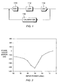
- a signal processing system for use in a communications satellite comprises an ADC 110, a DSP 112 connected to the output of the ADC 110, and a digital-to-analogue converter (DAC) 114 connected to the output of the DSP 112.
- An analogue signal is input to the ADC 110 and converted to a digital signal, which is then processed by the DSP 112.
- the processed digital signal is then converted back into the analogue domain by the DAC 114.
- a DSP calibrator 116 is used to check whether the signal phase is correctly preserved through the transitions from analogue to digital and back to analogue.
- the DSP calibrator 116 operates by injecting a known reference signal to the ADC 110 input, at a frequency chosen so as not to interfere with other frequencies present in the input signal being processed.
- the DSP calibrator 116 re-converts the analogue output of the DAC 114 back to a digital representation using its own ADC, i.e. a further ADC included in the calibrator 116, and then correlates this signal with its own local digital I, Q digital reference signals, from which a phase angle is measured.
- the phase-angle measurement leads to a phase-delay by systematic inference, given the known frequency of the reference signals. Therefore the DSP calibrator 116 can compare the reference signal at the DAC 114 output to the input reference signal to determine whether the reference signal phase has been preserved or whether phase errors have been introduced.
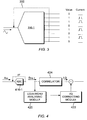
- Figure 2 is a graph plotting phase-delay error against input signal power for the system of Fig. 1 .
- the phase-delay error is measured in picoseconds (ps) and the input signal power is measured in decibels referenced to one milliwatt (dBm).
- the phase-delay error is the error inherent in measurements obtained by the DSP calibrator 116 for a reference signal comprising a constant tone at 9.80 megahertz (MHz).
- Fig. 2 at low input signal powers phase-delay errors of as much as several hundred ps are inferred as a result of the phase being incorrectly measured by the correlator, with the result that the phase angle is incorrectly measured by the correlator in the DSP calibrator 116.
- a leakage path 300 exists between the ADC output bus and the ADC input, meaning that the input signal can be influenced by current levels in the codeword presently being output by the ADC 316-1.
- Such a leakage path may be present in any conventional ADC since in practice the input and output are not perfectly isolated, meaning that a phase-delay anomaly may still occur regardless of the type of ADC used in the calibrator 116.
- the ADC output bus includes a plurality of signal lines each arranged to carry one bit of the output codeword.
- the ADC 316-1 is an 8-bit ADC, but the present invention is generally applicable to ADCs of any resolution. As the operating principles of ADCs are well-known, a detailed description will not be provided here.
- the level of current on each of the output lines depends on whether that bit of the codeword presently being output is set to 0 or 1, i.e. whether the voltage is set to low or high.
- the strength of the digital-to-analogue interference at any point in time will depend on the number of bits set to 1 in the codeword currently being output by the ADC 316-1. That is, the interference will be stronger when more bits are set to 1 because the mean output current will be higher.
- the present invention is not limited to use with such protocols. In other embodiments other electrical protocols may be used, for instance the level of current in both the 1 and 0 states may be the same, with only the current direction changing. In any case, regardless of the particular protocol used it may be assumed that the level of interference varies according to the logic values of bits in the codeword, e.g. the number of bits set to 1, and/or the number of 1-to-0 and 0-to-1 transitions relative to the preceding codeword, i.e. the difference between logic values of bits in the current codeword and the logic values of corresponding bits in the preceding codeword. In general terms, embodiments of the present invention can estimate the level of interference due to a codeword based on logic values of bits in the codeword.
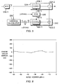
- the apparatus comprises a codeword analysing module 420 for analysing a codeword output by an ADC 416-1, a correlator 424 for obtaining I and Q values from the ADC output signal, and an I/Q correcting module 422 for obtaining in-phase (I) and quadrature (Q) corrections to be applied to the I and Q values obtained from the ADC output signal.
- a codeword analysing module 420 for analysing a codeword output by an ADC 416-1
- a correlator 424 for obtaining I and Q values from the ADC output signal
- an I/Q correcting module 422 for obtaining in-phase (I) and quadrature (Q) corrections to be applied to the I and Q values obtained from the ADC output signal.
- the codeword analysing module 420 is arranged to receive a codeword output by the ADC 416-1, and obtain information about an expected level of interference between the ADC output and input due to that codeword.
- the level of digital-to-analogue interference caused by a codeword being output by an ADC can be influenced by the mean current in the output signal lines and/or the number of bit transitions between consecutive codewords.
- the codeword analysing module 420 can be arranged to obtain the information about the expected level of interference based on the logic values of the bits in the codeword.
- the codeword analysing module 420 can be arranged to obtain information about the number of bits set to 1 in the received codeword.
- the information about the number of bits set to 1 can take various forms. For instance, in one embodiment the information may simply be the total number of bits set to 1, i.e. the Hamming weight of the codeword.
- the Hamming weight is the digit sum of a binary number, and can also be referred to as the "population count" or the "sideways sum".
- the Hamming weight of an 8-bit binary number can be any integer between 0 (i.e. all bits set to 0) and 8 (i.e. all bits set to 1).
- the output codeword 01101010 has a Hamming weight of 4 (0+1+1+0+1+0+1+0).
- the codeword analysing module 420 can be arranged to obtain a weighted digit sum of the received codeword, by multiplying each bit value (i.e. 1 or 0) by a corresponding predetermined weighting factor for that bit, and summing the weighted bits.
- This method can take into account the fact that not all output signal lines of the ADC may interfere equally with the ADC input.
- the coupling between any given signal line and the input may be influenced by the physical layout of the traces within the ADC. Bits transmitted on lines which interfere more strongly can be given a higher weighting than bits transmitted on lines which interfere less strongly.
- the weighting factors may differ for different ADC designs, and can be determined during setup and calibration of the system.
- the apparatus can account for digital-to-analogue interference due to static effects, specifically the ADC bus currents.
- the interference may also be influenced by dynamic effects such as ADC bus transitions, i.e. whether a particular bit changes from 1 to 0 or from 0 to 1 in consecutive codewords.
- the codeword analyser 420 can be arranged to compare each bit of the codeword to each corresponding bit of the preceding codeword output by the ADC, to determine the number of 0 to 1 bit transitions and the number of 1 to 0 bit transitions with respect to the preceding codeword. The information about the expected level of interference can then be obtained based on the number of transitions as well as the number of bits set to 1 in the current codeword. Furthermore, in some embodiments a weighted sum of the number of transitions can be computed, similar to the weighted digit sum of the codeword. This can account for the fact that transitions on a particular line of the ADC bus may interfere more strongly with the ADC input than transitions on another line of the ADC bus.
- information can be stored about the number of bits set to 1 for each one of a sequence of codewords output by the ADC.
- the codeword analyser 420 can then use this stored information, for example to calculate a derivative of the Hamming weight or weighted digit sum with respect to time, e.g. a first-order or second-order derivative.
- the derivative can be taken into account when estimating the level of interference, to account for higher-order effects.
- the first, second, third etc. difference may be used as a numerical approximation to the first, second, third etc. derivative.
- the finite difference is used as an approximation to the true mathematical derivative because the variable in question, e.g. the Hamming weight or weighted digit sum, is not a continuous variable but instead changes discontinuously between a limited number of discrete values.
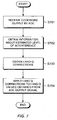
- Fig. 5 illustrates an apparatus for mitigating a phase anomaly in the output signal of an ADC, according to an embodiment of the present invention.
- the approach taken in Fig. 5 is to estimate the phase and amplitude of a digital-to-analogue interfering signal. This is done by setting the signal level at any point in time based on logic values of the bits in the current codeword, for example the Hamming weight, weighted digit sum, and/or the number of 1-to-0 and 0-to-1 bit transitions relative to the preceding codeword.
- the Hamming weight is used, and a Hamming weight calculating module 520 is provided to calculate the Hamming weight of a digital signal output by an ADC 516-1.
- the ADC 516-1 in the present embodiment is a 12-bit ADC.
- the Hamming weight of a 12-bit codeword can take an integer value between 0 and 12, and as such the Hamming weight calculating module 520 is provided with a 4-bit output bus to transmit any value between 0 and 12 in binary form.
- the output of the Hamming weight calculating module 520 is, in essence, used as a normalised representation of the level of interference due to that particular codeword with respect to other codewords.
- the output of the Hamming weight calculating module 520 over an extended period, during which a plurality of codewords are output and processed, can be considered as providing a model of the estimated interfering signal, in which the signal level of the estimated interfering signal at any time is given by the Hamming weight of the current codeword.
- the estimated interfering signal i.e. the output of the Hamming weight calculating module 520, is then scaled in amplitude to provide a quantified indication of the level of interference between the ADC output and input due to the current codeword.
- the output of the Hamming weight calculating module 520 is multiplied by a predetermined amplitude scaling parameter ⁇ .
- ⁇ is provided as an 8-bit number, such that a 12-bit scaled estimated interfering signal is obtained.
- the scaled signal is sent to a second correlator 522, which is similar to a first correlator 524 used to obtain I and Q values of the original (i.e. uncorrected) digital signal output by the ADC 516-1.
- a constant phase rotation is applied to the scaled signal to account for the fact that the codeword interfering with the analogue input signal corresponds to an earlier value of the signal, as opposed to the present value of the input signal. This arises because there is a latency associated with the analogue to digital conversion in the ADC 516-1, which for example may include a sample-and-hold circuit and pipeline.
- the phase-rotation can be applied directly to the scaled signal, or can be applied indirectly by correlating the scaled signal with a phase-rotated reference signal.
- the phase rotation is applied by generating two reference signals with a phase difference of ⁇ , and providing each reference signal to a different one of the correlators 522, 524.
- the value of ⁇ which in the present embodiment is an 8-bit number, is input to a reference signal generator 526.
- the reference signal generator 526 generates a first reference signal (REF1) to be sent to the first correlator 524, and a second reference signal (REF2) to be sent to the second correlator 522.
- ⁇ and ⁇ can be determined empirically during calibration of the system, by testing different values to determine which gives the most effective reduction in the phase-delay anomaly. Accordingly, knowledge of the actual interference mechanism or internal structure of the ADC 516-1 is not required.
- the parameter optimisation of ⁇ and ⁇ can therefore be obtained offline, i.e. before the system is put into use, and thereafter can be assumed to be time-invariant. In some embodiments however, means can be provided to periodically perform recalibration to update the vales of ⁇ and ⁇ , in order to account for effects such as ageing of system components.
- integral non-linearity (INL) and differential non-linearity (DNL) of the ADC 516-1 can be disregarded, but in some embodiments this may not be the case. If INL and DNL effects are not insignificant, ⁇ and ⁇ will be amplitude-dependent. This could be accounted for by determining different values of ⁇ and ⁇ to be used for different amplitudes.
- a quantified estimate of the level of interference currently present in the ADC output signal is obtained. Also, as a result of the correlation, in-phase (I) and quadrature (Q) values of the estimated interfering signal are obtained. These I and Q values can be used as corrections to be applied to the I and Q values of the output signal, which are obtained by the first correlator 524. Therefore the phase noise in the output signal can be reduced by subtracting the obtained I and Q corrections from the original I and Q values of the ADC output signal.
- the second correlator 522 includes a correlation part 522-1 for performing the correlation with the second reference signal REF2, and a bit shifting part 522-2 for performing a bit shift scaling function on the correlation result.
- the bit shifting part 522-2 is arranged to deal with the accumulated results of the correlating part 522-1, and hence operates at a slower rate than the correlating part 522-1.
- the bit shifting part 522-2 performs a bit shift scaling function to compensate for the bit-growth after the multiplication by ⁇ .
- the first correlator 524 includes a correlation part 524-1 and a subtraction part 524-2, the subtraction part being arranged to operate at the same slower rate as the bit shifting part 522-2 of the second correlator 522.
- both correlating parts 522-1, 524-1 operate at 48 MHz and the bit shifting part 522-2 and subtracting part 524-2 operate at 10 MHz, but these frequencies are only exemplary and other frequencies may be used.
- Figure 6 is a graph plotting phase-delay error against input signal power for the system of Fig. 5 , in which the phase anomaly due to digital-to-analogue interference has been reduced.
- the phase-delay error is measured in picoseconds (ps) and the input signal power is measured in decibels referenced to one milliwatt (dBm).
- the phase-delay error measurements are obtained for a reference signal comprising a constant tone at 9.80 megahertz (MHz).
- step S701 a codeword output by an ADC is received. Then, in step S702, information about an estimated level of interference between the ADC output and input due to the codeword is obtained, based on the logic values of bits in the codeword.
- the information may simply be the Hamming weight of the codeword or could be a weighted digit sum, and could also take into account such factors as bit transitions from one codeword to the next.
- step S703 I and Q are obtained corrections based on the obtained information.
- a Hamming weight signal can be correlated with a reference signal as described above with reference to Fig. 5 .
- step S704 the obtained corrections are applied to I and Q values obtained from the ADC output signal, to mitigate the phase anomaly arising due to digital-to-analogue interference in the ADC.
Landscapes
- Engineering & Computer Science (AREA)
- Theoretical Computer Science (AREA)
- Computer Networks & Wireless Communication (AREA)
- Signal Processing (AREA)
- Digital Transmission Methods That Use Modulated Carrier Waves (AREA)
- Analogue/Digital Conversion (AREA)
Claims (15)
- Verfahren zum Abschwächen einer Phasenanomalie im Ausgangssignal eines Analog-Digital-Wandlers ADC, wobei das Verfahren Folgendes beinhaltet:Empfangen mehrerer von dem ADC ausgegebener Codewörter;Einholen, für jedes der mehreren Codewörtern, von Informationen über einen geschätzten Interferenzpegel zwischen einem Ausgang des ADC und einem Eingang des ADC aufgrund des Codeworts auf der Basis der Logikwerte von Bits in dem Codewort;Einholen von In-Phase-I- und Quadratur-Q-Korrekturen des geschätzten Interferenzpegels auf der Basis der eingeholten Informationen; undAnwenden der I- und Q-Korrekturen auf von dem ADC-Ausgangssignal eingeholte I- und Q-Werte.
- Verfahren nach Anspruch 1, wobei das Einholen von Informationen über den geschätzten Interferenzpegel für jedes Codewort das Einholen der Informationen auf der Basis des Hamming-Gewichts des Codeworts beinhaltet.
- Verfahren nach Anspruch 1, wobei das Einholen von Informationen über den geschätzten Interferenzpegel für jedes Codewort Folgendes beinhaltet:Einholen einer gewichteten Quersumme des Codeworts durch Multiplizieren jedes Bits des Codeworts mit einem vorbestimmten Gewichtungsfaktor für dieses Bit und Summieren der gewichteten Bits; undEinholen der Informationen über den geschätzten Interferenzpegel auf der Basis der gewichteten Quersumme.
- Verfahren nach einem der vorherigen Ansprüche, wobei das Einholen von Informationen über den geschätzten Interferenzpegel für jedes Codewort ferner Folgendes beinhaltet:Vergleichen jedes Bits des Codeworts mit jedem entsprechenden Bit des vom ADC ausgegebenen vorhergehenden Codeworts, um die Anzahl von 0-zu-1-Bitübergängen und die Anzahl von 1-zu-0-Bitübergängen mit Bezug auf das vorherige Codewort zu ermitteln; undEinholen der Informationen über den geschätzten Interferenzpegel auf der Basis der Anzahl von 0-zu-1-Bitübergängen, der Anzahl von 1-zu-0-Bitübergängen und der Anzahl von im aktuellen Codewort auf 1 gesetzten Bits.
- Verfahren nach einem der vorherigen Ansprüche, wobei das Einholen von Informationen über den geschätzten Interferenzpegel für jedes Codewort ferner Folgendes beinhaltet:Speichern von Quersummeninformationen über die Anzahl von in jedem der mehreren Codewörter auf 1 gesetzten Bits; undEinholen der Informationen über den geschätzten Interferenzpegel aufgrund des aktuellen Codeworts auf der Basis der gespeicherten Quersummeninformationen.
- Verfahren nach einem der vorherigen Ansprüche, wobei die Informationen über den geschätzten Interferenzpegel für jedes Codewort einen Wert beinhalten, der einen relativen Interferenzpegel aufgrund des Codeworts repräsentiert, so dass mehrere der für die mehreren Codewörter eingeholten genannten Werte ein geschätztes Interferenzsignal definieren, und
wobei die I- und Q-Korrekturen durch Skalieren und Phasendrehen des geschätzten Interferenzsignals gemäß einem vorbestimmten Amplitudenskalierungsparameter und einem vorbestimmten Phasenrotationsparameter erhalten werden. - Verfahren nach Anspruch 6, das ferner Folgendes beinhaltet:Korrelieren des ADC-Ausgangssignals mit einem ersten Referenzsignal, um die I- und Q-Werte vom ADC-Ausgangssignal zu erhalten,wobei die Phasendrehung des geschätzten Interferenzsignals das Erzeugen eines zweiten Referenzsignals beinhaltet, das mit Bezug auf das erste Referenzsignal um einen durch den vorbestimmten Phasenrotationsparameter bestimmten Winkel phasengedreht ist, und Korrelieren des geschätzten Interferenzsignals mit dem zweiten Referenzsignal.
- Verfahren nach Anspruch 7, wobei die I- und Q-Korrekturen auf der Basis des Korrelationsergebnisses des Korrelierens des geschätzten Interferenzsignals mit dem zweiten Referenzsignal erhalten werden.
- Vorrichtung zum Abschwächen einer Phasenanomalie im Ausgangssignal eines Analog-Digital-Wandlers ADC, wobei die Vorrichtung Folgendes umfasst:Mittel (420; 520) zum Empfangen von mehreren vom ADC ausgegebenen Codewörtern und zum Einholen, für jedes der mehreren Codewörter, von Informationen über einen geschätzten Interferenzpegel zwischen einem Ausgang des ADC und einem Eingang des ADC aufgrund des Codewortes, auf der Basis der Logikwerte von Bits im Codewort;Mittel (422; 522) zum Einholen von In-Phase-I- und Quadratur-Q-Korrekturen des geschätzten Interferenzpegels auf der Basis der eingeholten Informationen; undMittel (524-2) zum Anwenden der I- und Q-Korrekturen auf von dem ADC-Ausgangssignal erhaltene I- und Q-Werte.
- Vorrichtung nach Anspruch 9, wobei das Mittel zum Einholen der Informationen über einen geschätzten Interferenzpegel ein Hamming-Gewichtskalkulator (520) ist.
- Vorrichtung nach Anspruch 9, wobei das Mittel zum Einholen der Informationen über einen geschätzten Interferenzpegel so ausgelegt ist, dass es für jedes Codewort eine gewichtete Quersumme des Codeworts durch Multiplizieren jedes Bits des Codeworts mit einem vorbestimmten Gewichtungsfaktor für dieses Bit und Summieren der gewichteten Bits einholt und die Informationen über den geschätzten Interferenzpegel auf der Basis der gewichteten Quersumme einholt.
- Vorrichtung nach Anspruch 9, 10 oder 11, wobei das Mittel zum Einholen der Informationen über einen geschätzten Interferenzpegel ferner ausgelegt ist zum:Vergleichen, für jedes Codewort, jedes Bits des Codeworts mit jedem entsprechenden Bit des vorhergehenden, vom ADC (416-1; 516-1) ausgegebenen Codeworts, Ermitteln der Anzahl von 0-zu-1-Bitübergängen und der Anzahl von 1-zu-0-Bitübergängen mit Bezug auf das vorhergehende Codewort, und Einholen der Informationen über den geschätzten Interferenzpegel auf der Basis der Anzahl von 0-zu-1-Bitübergängen, der Anzahl von 1-zu-0-Bitübergängen und der Anzahl von im aktuellen Codewort auf 1 gesetzten Bits.
- Vorrichtung nach einem der Ansprüche 9 bis 12, wobei das Mittel zum Einholen der Informationen über einen geschätzten Interferenzpegel ferner ausgelegt ist zum Speichern von Quersummeninformationen über die Anzahl von in jedem der mehreren Codewörter auf 1 gesetzten Bits und zum Einholen der Informationen über den geschätzten Interferenzpegel für jedes Codewort auf der Basis der gespeicherten Quersummeninformationen.
- Vorrichtung nach einem der Ansprüche 9 bis 13, wobei die Informationen über einen geschätzten Interferenzpegel einen Wert beinhalten, der einen relativen Interferenzpegel aufgrund des Codeworts repräsentiert, so dass mehrere der für die mehreren Codewörter eingeholten genannten Werte einen aktuellen Signalpegel eines geschätzten Interferenzsignals definieren, und
wobei das Mittel zum Einholen der I- und Q-Korrekturen Mittel zum Skalieren und Mittel (522-1) zum Phasendrehen des geschätzten Interferenzsignals gemäß einem vorbestimmten Amplitudenskalierungsparameter und einem vorbestimmten Phasenrotationsparameter umfasst. - Vorrichtung nach Anspruch 14, die Folgendes umfasst:einen Referenzsignalgenerator (526) zum Erzeugen eines ersten Referenzsignals (REF1) und eines zweiten Referenzsignals (REF2), das mit Bezug auf das erste Referenzsignal um einen Winkel phasengedreht ist, der durch den vorbestimmten Phasenrotationsparameter bestimmt wird, undeinen ersten Korrelator (524-1) zum Korrelieren des ADC-Ausgangssignals mit dem ersten Referenzsignal, um die I- und Q-Werte des ADC-Ausgangssignals zu erhalten;wobei das Mittel zum Skalieren und Phasendrehen des geschätzten Interferenzsignals einen zweiten Korrelator (522-1) zum Korrelieren des geschätzten Interferenzsignals mit dem zweiten Referenzsignal beinhaltet, um die Phasendrehung auf das geschätzte Interferenzsignal anzuwenden.
Priority Applications (1)
| Application Number | Priority Date | Filing Date | Title |
|---|---|---|---|
| EP13713831.9A EP2831998B8 (de) | 2012-03-30 | 2013-03-26 | Abschwächung einer phasenanomalie in einem ausgangssignal eines analog-digital-wandlers |
Applications Claiming Priority (3)
| Application Number | Priority Date | Filing Date | Title |
|---|---|---|---|
| EP12275035.9A EP2645576A1 (de) | 2012-03-30 | 2012-03-30 | Abschwächung einer Phasenanomalie in einem Ausgangssignal eines Analog-Digital-Wandlers |
| PCT/EP2013/056397 WO2013144142A1 (en) | 2012-03-30 | 2013-03-26 | Mitigating a phase anomaly in an analogue-to-digital converter output signal |
| EP13713831.9A EP2831998B8 (de) | 2012-03-30 | 2013-03-26 | Abschwächung einer phasenanomalie in einem ausgangssignal eines analog-digital-wandlers |
Publications (3)
| Publication Number | Publication Date |
|---|---|
| EP2831998A1 EP2831998A1 (de) | 2015-02-04 |
| EP2831998B1 true EP2831998B1 (de) | 2016-07-27 |
| EP2831998B8 EP2831998B8 (de) | 2017-03-22 |
Family
ID=48045483
Family Applications (2)
| Application Number | Title | Priority Date | Filing Date |
|---|---|---|---|
| EP12275035.9A Ceased EP2645576A1 (de) | 2012-03-30 | 2012-03-30 | Abschwächung einer Phasenanomalie in einem Ausgangssignal eines Analog-Digital-Wandlers |
| EP13713831.9A Active EP2831998B8 (de) | 2012-03-30 | 2013-03-26 | Abschwächung einer phasenanomalie in einem ausgangssignal eines analog-digital-wandlers |
Family Applications Before (1)
| Application Number | Title | Priority Date | Filing Date |
|---|---|---|---|
| EP12275035.9A Ceased EP2645576A1 (de) | 2012-03-30 | 2012-03-30 | Abschwächung einer Phasenanomalie in einem Ausgangssignal eines Analog-Digital-Wandlers |
Country Status (6)
| Country | Link |
|---|---|
| US (2) | US20150078496A1 (de) |
| EP (2) | EP2645576A1 (de) |
| JP (1) | JP6186611B2 (de) |
| CA (1) | CA2869055C (de) |
| ES (1) | ES2605491T3 (de) |
| WO (1) | WO2013144142A1 (de) |
Families Citing this family (2)
| Publication number | Priority date | Publication date | Assignee | Title |
|---|---|---|---|---|
| JP6478613B2 (ja) * | 2014-12-16 | 2019-03-06 | 株式会社東芝 | 受信装置、通信システム、および干渉検出方法 |
| JP7674215B2 (ja) * | 2021-09-30 | 2025-05-09 | トヨタ自動車株式会社 | 情報処理装置、送信側装置、及び、方法 |
Family Cites Families (10)
| Publication number | Priority date | Publication date | Assignee | Title |
|---|---|---|---|---|
| SE514809C2 (sv) | 1994-07-13 | 2001-04-30 | Hd Divine Ab | Metod och anordning för synkronisering av sändare och mottagare i digitalt system |
| US6301221B1 (en) * | 1997-09-10 | 2001-10-09 | Hewlett-Packard Company | Methods and apparatus for encoding data |
| EP1371200B1 (de) * | 2001-03-01 | 2011-10-12 | Broadcom Corporation | Ausgleich von durch kanal oder empfänger verursachten verzerrungen bei paralleler übertragung |
| DE10305972A1 (de) * | 2003-02-13 | 2004-09-02 | Micronas Gmbh | Kompensationsschaltungsanordnung und Kompensationsverfahren zum Kompensieren von nicht-linearen Verzerrungen eines AD-Wandlers |
| US6836227B2 (en) * | 2003-02-25 | 2004-12-28 | Advantest Corporation | Digitizer module, a waveform generating module, a converting method, a waveform generating method and a recording medium for recording a program thereof |
| US7266161B1 (en) * | 2003-06-26 | 2007-09-04 | Rockwell Collins, Inc. | Efficient method and apparatus for parallel processing for use with high-speed single-bit sampling |
| DE102004049348A1 (de) * | 2004-10-08 | 2006-04-20 | Micronas Gmbh | Verfahren sowie Einrichtung zur Kompensation von Kennlinienfehlern eines Analog-Digital-Wandlers |
| JPWO2011033571A1 (ja) * | 2009-09-18 | 2013-02-07 | 株式会社東芝 | 受信機 |
| JP5517125B2 (ja) | 2010-02-05 | 2014-06-11 | 国立大学法人 東京大学 | 細胞測定装置 |
| JP5361927B2 (ja) * | 2011-03-14 | 2013-12-04 | 株式会社東芝 | 無線受信装置 |
-
2012
- 2012-03-30 EP EP12275035.9A patent/EP2645576A1/de not_active Ceased
-
2013
- 2013-03-26 EP EP13713831.9A patent/EP2831998B8/de active Active
- 2013-03-26 ES ES13713831.9T patent/ES2605491T3/es active Active
- 2013-03-26 JP JP2015502302A patent/JP6186611B2/ja active Active
- 2013-03-26 CA CA2869055A patent/CA2869055C/en active Active
- 2013-03-26 WO PCT/EP2013/056397 patent/WO2013144142A1/en not_active Ceased
-
2014
- 2014-09-30 US US14/502,938 patent/US20150078496A1/en not_active Abandoned
-
2016
- 2016-01-28 US US15/009,789 patent/US9628123B2/en not_active Expired - Fee Related
Also Published As
| Publication number | Publication date |
|---|---|
| CA2869055A1 (en) | 2013-10-03 |
| JP2015515204A (ja) | 2015-05-21 |
| US9628123B2 (en) | 2017-04-18 |
| ES2605491T3 (es) | 2017-03-14 |
| CA2869055C (en) | 2020-07-14 |
| US20150078496A1 (en) | 2015-03-19 |
| EP2645576A1 (de) | 2013-10-02 |
| JP6186611B2 (ja) | 2017-08-30 |
| WO2013144142A1 (en) | 2013-10-03 |
| EP2831998A1 (de) | 2015-02-04 |
| EP2831998B8 (de) | 2017-03-22 |
| US20160248461A1 (en) | 2016-08-25 |
Similar Documents
| Publication | Publication Date | Title |
|---|---|---|
| JP2008526152A (ja) | 送信装置 | |
| EP2961072B1 (de) | Mehrkanaliger zeitverschachtelter analog-digital-wandler | |
| US7839323B2 (en) | Error estimation and correction in a two-channel time-interleaved analog-to-digital converter | |
| EP1829314B1 (de) | Kalibrierung von Amplituden- und Phasenungleichgewicht sowie DC-Offset eines analogen I/Q-Modulators bei einem Hochfrequenzsender | |
| US12425039B2 (en) | Time-interleaved ADC skew correction | |
| EP2831998B1 (de) | Abschwächung einer phasenanomalie in einem ausgangssignal eines analog-digital-wandlers | |
| CA2924980C (en) | Phase angle measurement using residue number system analogue-to-digital conversion | |
| KR20140105409A (ko) | Iq 변조기에서의 dc 오프셋의 측정 | |
| US8060037B2 (en) | Circuit and method of calibrating direct current offset in wireless communication device | |
| KR20090085283A (ko) | 아날로그 디지털 변환기의 오차 보정 장치 및 방법 | |
| US11075644B2 (en) | Efficient all-digital domain calibration architecture for a successive approximation register analog-to-digital converter | |
| CN101552753B (zh) | 无线通信装置的直流偏移校正电路及其校正方法 | |
| US12224759B2 (en) | Apparatus and method for calibrating mismatches of time-interleaved analog-to-digital converter | |
| US20120300876A1 (en) | Quadrature modulator, signal generating device, and quadrature modulation method | |
| Serov et al. | Application of harmonic functions to estimate the active power measurement error caused by ADC nonlinearity and quantization error | |
| JP4574531B2 (ja) | 送信機 | |
| US20220263516A1 (en) | Measurement unit configured to provide a measurement result value using calculated values | |
| Arpaia et al. | Compensation of intrinsic nonlinearity of SAR ADCs | |
| US20050111577A1 (en) | Method for residual carrier suppression in an arrangement which has a vector modulator | |
| KR101158038B1 (ko) | A/d 변환 시 고조파를 감소시키기 위한 방법 | |
| Medawar | Pipeline Analog-Digital Converters Dynamic Error Modeling for Calibration: Integral Nonlinearity Modeling, Pipeline ADC Calibration, Wireless Channel K-Factor Estimation | |
| Mendonça et al. | Estimation of analogue-to-digital converter's signal-to-noise plus distortion ratio using the code histogram method | |
| Kim et al. | Digital Background Self-calibration for High Resolution Analog to Digital Converters | |
| JP2008167494A (ja) | 送信機 |
Legal Events
| Date | Code | Title | Description |
|---|---|---|---|
| PUAI | Public reference made under article 153(3) epc to a published international application that has entered the european phase |
Free format text: ORIGINAL CODE: 0009012 |
|
| 17P | Request for examination filed |
Effective date: 20140929 |
|
| AK | Designated contracting states |
Kind code of ref document: A1 Designated state(s): AL AT BE BG CH CY CZ DE DK EE ES FI FR GB GR HR HU IE IS IT LI LT LU LV MC MK MT NL NO PL PT RO RS SE SI SK SM TR |
|
| AX | Request for extension of the european patent |
Extension state: BA ME |
|
| DAX | Request for extension of the european patent (deleted) | ||
| GRAP | Despatch of communication of intention to grant a patent |
Free format text: ORIGINAL CODE: EPIDOSNIGR1 |
|
| INTG | Intention to grant announced |
Effective date: 20151223 |
|
| GRAP | Despatch of communication of intention to grant a patent |
Free format text: ORIGINAL CODE: EPIDOSNIGR1 |
|
| GRAS | Grant fee paid |
Free format text: ORIGINAL CODE: EPIDOSNIGR3 |
|
| GRAA | (expected) grant |
Free format text: ORIGINAL CODE: 0009210 |
|
| INTG | Intention to grant announced |
Effective date: 20160531 |
|
| AK | Designated contracting states |
Kind code of ref document: B1 Designated state(s): AL AT BE BG CH CY CZ DE DK EE ES FI FR GB GR HR HU IE IS IT LI LT LU LV MC MK MT NL NO PL PT RO RS SE SI SK SM TR |
|
| REG | Reference to a national code |
Ref country code: GB Ref legal event code: FG4D |
|
| REG | Reference to a national code |
Ref country code: CH Ref legal event code: EP |
|
| REG | Reference to a national code |
Ref country code: AT Ref legal event code: REF Ref document number: 816519 Country of ref document: AT Kind code of ref document: T Effective date: 20160815 |
|
| REG | Reference to a national code |
Ref country code: IE Ref legal event code: FG4D |
|
| REG | Reference to a national code |
Ref country code: DE Ref legal event code: R096 Ref document number: 602013009842 Country of ref document: DE |
|
| REG | Reference to a national code |
Ref country code: SE Ref legal event code: TRGR |
|
| REG | Reference to a national code |
Ref country code: LT Ref legal event code: MG4D |
|
| REG | Reference to a national code |
Ref country code: DE Ref legal event code: R081 Ref document number: 602013009842 Country of ref document: DE Owner name: AIRBUS DEFENCE AND SPACE LTD., STEVENAGE, GB Free format text: FORMER OWNER: ASTRIUM LIMITED, STEVENAGE, HERTFORDSHIRE, GB |
|
| REG | Reference to a national code |
Ref country code: NL Ref legal event code: FP |
|
| REG | Reference to a national code |
Ref country code: AT Ref legal event code: MK05 Ref document number: 816519 Country of ref document: AT Kind code of ref document: T Effective date: 20160727 |
|
| GRAT | Correction requested after decision to grant or after decision to maintain patent in amended form |
Free format text: ORIGINAL CODE: EPIDOSNCDEC |
|
| RAP2 | Party data changed (patent owner data changed or rights of a patent transferred) |
Owner name: AIRBUS DEFENCE AND SPACE LIMITED |
|
| PG25 | Lapsed in a contracting state [announced via postgrant information from national office to epo] |
Ref country code: FI Free format text: LAPSE BECAUSE OF FAILURE TO SUBMIT A TRANSLATION OF THE DESCRIPTION OR TO PAY THE FEE WITHIN THE PRESCRIBED TIME-LIMIT Effective date: 20160727 Ref country code: LT Free format text: LAPSE BECAUSE OF FAILURE TO SUBMIT A TRANSLATION OF THE DESCRIPTION OR TO PAY THE FEE WITHIN THE PRESCRIBED TIME-LIMIT Effective date: 20160727 Ref country code: HR Free format text: LAPSE BECAUSE OF FAILURE TO SUBMIT A TRANSLATION OF THE DESCRIPTION OR TO PAY THE FEE WITHIN THE PRESCRIBED TIME-LIMIT Effective date: 20160727 Ref country code: IT Free format text: LAPSE BECAUSE OF FAILURE TO SUBMIT A TRANSLATION OF THE DESCRIPTION OR TO PAY THE FEE WITHIN THE PRESCRIBED TIME-LIMIT Effective date: 20160727 Ref country code: RS Free format text: LAPSE BECAUSE OF FAILURE TO SUBMIT A TRANSLATION OF THE DESCRIPTION OR TO PAY THE FEE WITHIN THE PRESCRIBED TIME-LIMIT Effective date: 20160727 Ref country code: IS Free format text: LAPSE BECAUSE OF FAILURE TO SUBMIT A TRANSLATION OF THE DESCRIPTION OR TO PAY THE FEE WITHIN THE PRESCRIBED TIME-LIMIT Effective date: 20161127 Ref country code: NO Free format text: LAPSE BECAUSE OF FAILURE TO SUBMIT A TRANSLATION OF THE DESCRIPTION OR TO PAY THE FEE WITHIN THE PRESCRIBED TIME-LIMIT Effective date: 20161027 |
|
| PG25 | Lapsed in a contracting state [announced via postgrant information from national office to epo] |
Ref country code: LV Free format text: LAPSE BECAUSE OF FAILURE TO SUBMIT A TRANSLATION OF THE DESCRIPTION OR TO PAY THE FEE WITHIN THE PRESCRIBED TIME-LIMIT Effective date: 20160727 Ref country code: PL Free format text: LAPSE BECAUSE OF FAILURE TO SUBMIT A TRANSLATION OF THE DESCRIPTION OR TO PAY THE FEE WITHIN THE PRESCRIBED TIME-LIMIT Effective date: 20160727 Ref country code: AT Free format text: LAPSE BECAUSE OF FAILURE TO SUBMIT A TRANSLATION OF THE DESCRIPTION OR TO PAY THE FEE WITHIN THE PRESCRIBED TIME-LIMIT Effective date: 20160727 Ref country code: PT Free format text: LAPSE BECAUSE OF FAILURE TO SUBMIT A TRANSLATION OF THE DESCRIPTION OR TO PAY THE FEE WITHIN THE PRESCRIBED TIME-LIMIT Effective date: 20161128 Ref country code: GR Free format text: LAPSE BECAUSE OF FAILURE TO SUBMIT A TRANSLATION OF THE DESCRIPTION OR TO PAY THE FEE WITHIN THE PRESCRIBED TIME-LIMIT Effective date: 20161028 Ref country code: BE Free format text: LAPSE BECAUSE OF FAILURE TO SUBMIT A TRANSLATION OF THE DESCRIPTION OR TO PAY THE FEE WITHIN THE PRESCRIBED TIME-LIMIT Effective date: 20160727 |
|
| REG | Reference to a national code |
Ref country code: ES Ref legal event code: FG2A Ref document number: 2605491 Country of ref document: ES Kind code of ref document: T3 Effective date: 20170314 |
|
| REG | Reference to a national code |
Ref country code: FR Ref legal event code: PLFP Year of fee payment: 5 |
|
| PG25 | Lapsed in a contracting state [announced via postgrant information from national office to epo] |
Ref country code: RO Free format text: LAPSE BECAUSE OF FAILURE TO SUBMIT A TRANSLATION OF THE DESCRIPTION OR TO PAY THE FEE WITHIN THE PRESCRIBED TIME-LIMIT Effective date: 20160727 Ref country code: EE Free format text: LAPSE BECAUSE OF FAILURE TO SUBMIT A TRANSLATION OF THE DESCRIPTION OR TO PAY THE FEE WITHIN THE PRESCRIBED TIME-LIMIT Effective date: 20160727 |
|
| REG | Reference to a national code |
Ref country code: DE Ref legal event code: R097 Ref document number: 602013009842 Country of ref document: DE |
|
| PG25 | Lapsed in a contracting state [announced via postgrant information from national office to epo] |
Ref country code: SM Free format text: LAPSE BECAUSE OF FAILURE TO SUBMIT A TRANSLATION OF THE DESCRIPTION OR TO PAY THE FEE WITHIN THE PRESCRIBED TIME-LIMIT Effective date: 20160727 Ref country code: BG Free format text: LAPSE BECAUSE OF FAILURE TO SUBMIT A TRANSLATION OF THE DESCRIPTION OR TO PAY THE FEE WITHIN THE PRESCRIBED TIME-LIMIT Effective date: 20161027 Ref country code: SK Free format text: LAPSE BECAUSE OF FAILURE TO SUBMIT A TRANSLATION OF THE DESCRIPTION OR TO PAY THE FEE WITHIN THE PRESCRIBED TIME-LIMIT Effective date: 20160727 Ref country code: CZ Free format text: LAPSE BECAUSE OF FAILURE TO SUBMIT A TRANSLATION OF THE DESCRIPTION OR TO PAY THE FEE WITHIN THE PRESCRIBED TIME-LIMIT Effective date: 20160727 Ref country code: DK Free format text: LAPSE BECAUSE OF FAILURE TO SUBMIT A TRANSLATION OF THE DESCRIPTION OR TO PAY THE FEE WITHIN THE PRESCRIBED TIME-LIMIT Effective date: 20160727 |
|
| PLBE | No opposition filed within time limit |
Free format text: ORIGINAL CODE: 0009261 |
|
| STAA | Information on the status of an ep patent application or granted ep patent |
Free format text: STATUS: NO OPPOSITION FILED WITHIN TIME LIMIT |
|
| 26N | No opposition filed |
Effective date: 20170502 |
|
| PG25 | Lapsed in a contracting state [announced via postgrant information from national office to epo] |
Ref country code: SI Free format text: LAPSE BECAUSE OF FAILURE TO SUBMIT A TRANSLATION OF THE DESCRIPTION OR TO PAY THE FEE WITHIN THE PRESCRIBED TIME-LIMIT Effective date: 20160727 |
|
| REG | Reference to a national code |
Ref country code: CH Ref legal event code: PL |
|
| PG25 | Lapsed in a contracting state [announced via postgrant information from national office to epo] |
Ref country code: MC Free format text: LAPSE BECAUSE OF FAILURE TO SUBMIT A TRANSLATION OF THE DESCRIPTION OR TO PAY THE FEE WITHIN THE PRESCRIBED TIME-LIMIT Effective date: 20160727 |
|
| REG | Reference to a national code |
Ref country code: IE Ref legal event code: MM4A |
|
| PG25 | Lapsed in a contracting state [announced via postgrant information from national office to epo] |
Ref country code: LU Free format text: LAPSE BECAUSE OF NON-PAYMENT OF DUE FEES Effective date: 20170326 |
|
| PG25 | Lapsed in a contracting state [announced via postgrant information from national office to epo] |
Ref country code: LI Free format text: LAPSE BECAUSE OF NON-PAYMENT OF DUE FEES Effective date: 20170331 Ref country code: IE Free format text: LAPSE BECAUSE OF NON-PAYMENT OF DUE FEES Effective date: 20170326 Ref country code: CH Free format text: LAPSE BECAUSE OF NON-PAYMENT OF DUE FEES Effective date: 20170331 |
|
| REG | Reference to a national code |
Ref country code: FR Ref legal event code: PLFP Year of fee payment: 6 |
|
| PG25 | Lapsed in a contracting state [announced via postgrant information from national office to epo] |
Ref country code: MT Free format text: LAPSE BECAUSE OF NON-PAYMENT OF DUE FEES Effective date: 20170326 |
|
| PG25 | Lapsed in a contracting state [announced via postgrant information from national office to epo] |
Ref country code: AL Free format text: LAPSE BECAUSE OF FAILURE TO SUBMIT A TRANSLATION OF THE DESCRIPTION OR TO PAY THE FEE WITHIN THE PRESCRIBED TIME-LIMIT Effective date: 20160727 |
|
| PG25 | Lapsed in a contracting state [announced via postgrant information from national office to epo] |
Ref country code: HU Free format text: LAPSE BECAUSE OF FAILURE TO SUBMIT A TRANSLATION OF THE DESCRIPTION OR TO PAY THE FEE WITHIN THE PRESCRIBED TIME-LIMIT; INVALID AB INITIO Effective date: 20130326 |
|
| PG25 | Lapsed in a contracting state [announced via postgrant information from national office to epo] |
Ref country code: CY Free format text: LAPSE BECAUSE OF FAILURE TO SUBMIT A TRANSLATION OF THE DESCRIPTION OR TO PAY THE FEE WITHIN THE PRESCRIBED TIME-LIMIT Effective date: 20160727 |
|
| PG25 | Lapsed in a contracting state [announced via postgrant information from national office to epo] |
Ref country code: MK Free format text: LAPSE BECAUSE OF FAILURE TO SUBMIT A TRANSLATION OF THE DESCRIPTION OR TO PAY THE FEE WITHIN THE PRESCRIBED TIME-LIMIT Effective date: 20160727 |
|
| PG25 | Lapsed in a contracting state [announced via postgrant information from national office to epo] |
Ref country code: TR Free format text: LAPSE BECAUSE OF FAILURE TO SUBMIT A TRANSLATION OF THE DESCRIPTION OR TO PAY THE FEE WITHIN THE PRESCRIBED TIME-LIMIT Effective date: 20160727 |
|
| PGFP | Annual fee paid to national office [announced via postgrant information from national office to epo] |
Ref country code: SE Payment date: 20200323 Year of fee payment: 8 Ref country code: NL Payment date: 20200319 Year of fee payment: 8 |
|
| REG | Reference to a national code |
Ref country code: DE Ref legal event code: R082 Ref document number: 602013009842 Country of ref document: DE Representative=s name: VENNER SHIPLEY GERMANY LLP, DE Ref country code: DE Ref legal event code: R082 Ref document number: 602013009842 Country of ref document: DE Representative=s name: VENNER SHIPLEY LLP, DE |
|
| REG | Reference to a national code |
Ref country code: NL Ref legal event code: MM Effective date: 20210401 |
|
| PG25 | Lapsed in a contracting state [announced via postgrant information from national office to epo] |
Ref country code: SE Free format text: LAPSE BECAUSE OF NON-PAYMENT OF DUE FEES Effective date: 20210327 Ref country code: NL Free format text: LAPSE BECAUSE OF NON-PAYMENT OF DUE FEES Effective date: 20210401 |
|
| PGFP | Annual fee paid to national office [announced via postgrant information from national office to epo] |
Ref country code: DE Payment date: 20250319 Year of fee payment: 13 |
|
| PGFP | Annual fee paid to national office [announced via postgrant information from national office to epo] |
Ref country code: FR Payment date: 20250325 Year of fee payment: 13 |
|
| PGFP | Annual fee paid to national office [announced via postgrant information from national office to epo] |
Ref country code: GB Payment date: 20250321 Year of fee payment: 13 |
|
| PGFP | Annual fee paid to national office [announced via postgrant information from national office to epo] |
Ref country code: ES Payment date: 20250429 Year of fee payment: 13 |