EP2831925B1 - Electronic component housing with heat sink - Google Patents
Electronic component housing with heat sink Download PDFInfo
- Publication number
- EP2831925B1 EP2831925B1 EP13768875.0A EP13768875A EP2831925B1 EP 2831925 B1 EP2831925 B1 EP 2831925B1 EP 13768875 A EP13768875 A EP 13768875A EP 2831925 B1 EP2831925 B1 EP 2831925B1
- Authority
- EP
- European Patent Office
- Prior art keywords
- electronic component
- photovoltaic assembly
- photovoltaic
- opening
- component housing
- Prior art date
- Legal status (The legal status is an assumption and is not a legal conclusion. Google has not performed a legal analysis and makes no representation as to the accuracy of the status listed.)
- Not-in-force
Links
- 239000000853 adhesive Substances 0.000 claims description 5
- 230000001070 adhesive effect Effects 0.000 claims description 5
- 238000005452 bending Methods 0.000 claims description 5
- 238000004891 communication Methods 0.000 claims description 5
- 229920000642 polymer Polymers 0.000 claims description 5
- 229910052782 aluminium Inorganic materials 0.000 claims description 3
- XAGFODPZIPBFFR-UHFFFAOYSA-N aluminium Chemical compound [Al] XAGFODPZIPBFFR-UHFFFAOYSA-N 0.000 claims description 3
- 239000011521 glass Substances 0.000 claims description 3
- 239000012530 fluid Substances 0.000 claims description 2
- 238000010586 diagram Methods 0.000 description 14
- 230000000712 assembly Effects 0.000 description 10
- 238000000429 assembly Methods 0.000 description 10
- 239000000463 material Substances 0.000 description 6
- 238000001816 cooling Methods 0.000 description 5
- 239000008393 encapsulating agent Substances 0.000 description 5
- 230000005855 radiation Effects 0.000 description 4
- 230000000694 effects Effects 0.000 description 2
- 230000002401 inhibitory effect Effects 0.000 description 2
- RYGMFSIKBFXOCR-UHFFFAOYSA-N Copper Chemical compound [Cu] RYGMFSIKBFXOCR-UHFFFAOYSA-N 0.000 description 1
- 230000009471 action Effects 0.000 description 1
- 230000015556 catabolic process Effects 0.000 description 1
- 230000001010 compromised effect Effects 0.000 description 1
- 230000003750 conditioning effect Effects 0.000 description 1
- 239000000470 constituent Substances 0.000 description 1
- 238000010276 construction Methods 0.000 description 1
- 229910052802 copper Inorganic materials 0.000 description 1
- 239000010949 copper Substances 0.000 description 1
- 238000006731 degradation reaction Methods 0.000 description 1
- 230000001419 dependent effect Effects 0.000 description 1
- 230000005611 electricity Effects 0.000 description 1
- 230000008676 import Effects 0.000 description 1
- 238000009413 insulation Methods 0.000 description 1
- 230000007246 mechanism Effects 0.000 description 1
- 229910052751 metal Inorganic materials 0.000 description 1
- 239000002184 metal Substances 0.000 description 1
- 238000000034 method Methods 0.000 description 1
- 230000008569 process Effects 0.000 description 1
- 230000009467 reduction Effects 0.000 description 1
- 239000012780 transparent material Substances 0.000 description 1
Images


Classifications
-
- H—ELECTRICITY
- H05—ELECTRIC TECHNIQUES NOT OTHERWISE PROVIDED FOR
- H05K—PRINTED CIRCUITS; CASINGS OR CONSTRUCTIONAL DETAILS OF ELECTRIC APPARATUS; MANUFACTURE OF ASSEMBLAGES OF ELECTRICAL COMPONENTS
- H05K7/00—Constructional details common to different types of electric apparatus
- H05K7/20—Modifications to facilitate cooling, ventilating, or heating
- H05K7/2039—Modifications to facilitate cooling, ventilating, or heating characterised by the heat transfer by conduction from the heat generating element to a dissipating body
-
- H—ELECTRICITY
- H02—GENERATION; CONVERSION OR DISTRIBUTION OF ELECTRIC POWER
- H02S—GENERATION OF ELECTRIC POWER BY CONVERSION OF INFRARED RADIATION, VISIBLE LIGHT OR ULTRAVIOLET LIGHT, e.g. USING PHOTOVOLTAIC [PV] MODULES
- H02S40/00—Components or accessories in combination with PV modules, not provided for in groups H02S10/00 - H02S30/00
- H02S40/30—Electrical components
- H02S40/34—Electrical components comprising specially adapted electrical connection means to be structurally associated with the PV module, e.g. junction boxes
- H02S40/345—Electrical components comprising specially adapted electrical connection means to be structurally associated with the PV module, e.g. junction boxes with cooling means associated with the electrical connection means, e.g. cooling means associated with or applied to the junction box
-
- H—ELECTRICITY
- H01—ELECTRIC ELEMENTS
- H01L—SEMICONDUCTOR DEVICES NOT COVERED BY CLASS H10
- H01L31/00—Semiconductor devices sensitive to infrared radiation, light, electromagnetic radiation of shorter wavelength or corpuscular radiation and specially adapted either for the conversion of the energy of such radiation into electrical energy or for the control of electrical energy by such radiation; Processes or apparatus specially adapted for the manufacture or treatment thereof or of parts thereof; Details thereof
- H01L31/02—Details
- H01L31/024—Arrangements for cooling, heating, ventilating or temperature compensation
-
- H—ELECTRICITY
- H01—ELECTRIC ELEMENTS
- H01L—SEMICONDUCTOR DEVICES NOT COVERED BY CLASS H10
- H01L31/00—Semiconductor devices sensitive to infrared radiation, light, electromagnetic radiation of shorter wavelength or corpuscular radiation and specially adapted either for the conversion of the energy of such radiation into electrical energy or for the control of electrical energy by such radiation; Processes or apparatus specially adapted for the manufacture or treatment thereof or of parts thereof; Details thereof
- H01L31/04—Semiconductor devices sensitive to infrared radiation, light, electromagnetic radiation of shorter wavelength or corpuscular radiation and specially adapted either for the conversion of the energy of such radiation into electrical energy or for the control of electrical energy by such radiation; Processes or apparatus specially adapted for the manufacture or treatment thereof or of parts thereof; Details thereof adapted as photovoltaic [PV] conversion devices
- H01L31/042—PV modules or arrays of single PV cells
- H01L31/048—Encapsulation of modules
- H01L31/049—Protective back sheets
-
- Y—GENERAL TAGGING OF NEW TECHNOLOGICAL DEVELOPMENTS; GENERAL TAGGING OF CROSS-SECTIONAL TECHNOLOGIES SPANNING OVER SEVERAL SECTIONS OF THE IPC; TECHNICAL SUBJECTS COVERED BY FORMER USPC CROSS-REFERENCE ART COLLECTIONS [XRACs] AND DIGESTS
- Y02—TECHNOLOGIES OR APPLICATIONS FOR MITIGATION OR ADAPTATION AGAINST CLIMATE CHANGE
- Y02E—REDUCTION OF GREENHOUSE GAS [GHG] EMISSIONS, RELATED TO ENERGY GENERATION, TRANSMISSION OR DISTRIBUTION
- Y02E10/00—Energy generation through renewable energy sources
- Y02E10/50—Photovoltaic [PV] energy
Definitions
- Embodiments of the subject matter described herein relate generally to photovoltaic assemblies including solar cells, photovoltaic modules and associated electronic components. More particularly, one or more embodiments of the present invention relate to photovoltaic modules, electronic housing components and heat sinks.
- JP H11 251614 A relates to a solar battery module having a plurality of solar battery cells, a terminal box, a by-pass diode and a cover.
- EP 0 793 278 A2 relates to a photo-voltaic apparatus having a plurality of photo-voltaic cells and an inverter.
- JP 2007 166721 A relates to an electric power generator having peltier elements and a cooling panel.
- FR 2 914 754 A1 relates to a light concentration device having a plate, a refractive index gradient existing between two principal faces of the plate, and a diffraction grating functioning in reflection or semi-reflection that cooperates with one of the principal faces of the plate having the highest refractive index.
- Solar cells are well known devices for converting solar radiation to electrical energy.
- Several solar cells can be connected to together to form a solar cell array.
- the solar cell array can be packaged into a photovoltaic (PV) module using various processes and encapsulant materials.
- Electronic components and wiring are required to convert, gather and transfer generated electric current. These electronic components are usually mounted close to the back of a photovoltaic module so that shipping density of the photovoltaic modules is not compromised.
- the electronic components can generate or trap heat which can cause the encapsulant materials to degrade at an accelerated rate. The heat can also permanently damage the cells inside photovoltaic module, or cause temporary performance degradation.
- One or more embodiments of the present invention pertain to photovoltaic assemblies that present alternative means of transferring heat from the electronics components to an ambient environment.
- inhibit is used to describe a reducing or minimizing effect. When a component or feature is described as inhibiting an action, motion, or condition it may completely prevent the result or outcome or future state completely. Additionally, “inhibit” can also refer to a reduction or lessening of the outcome, performance, and/or effect which might otherwise occur. Accordingly, when a component, element, or feature is referred to as inhibiting a result or state, it need not completely prevent or eliminate the result or state.
- a photovoltaic assembly for converting solar radiation to electrical energy is defined in claim 1. Further advantageous embodiments are defined in the dependent claims.
- Coupled means that one element/node/feature is directly or indirectly joined to (or directly or indirectly communicates with) another element/node/feature, and not necessarily mechanically coupled.
- FIGS. 1-20 illustrate various embodiments of a photovoltaic assembly for converting solar radiation to electrical energy. Numerous specific details are provided, such as examples of apparatuses and components to provide a thorough understanding of at least some embodiments of the present invention. It is to be understood, however, that other embodiments of the present invention can be practiced without one or more of the specific details set forth. In other instances, well-known details are not shown or described in order to avoid obscuring aspects of certain embodiments of the present invention.
- FIG. 1 illustrates a photovoltaic module 110 having a front side 112 that faces the sun during normal operation and a back side 114 opposite the front side 112.
- the photovoltaic module 110 has a frame 118 and a laminate 116 containing a plurality of solar cells 117.
- the solar cells 117 face the front side 112.
- the laminate 116 can include one or more encapsulating layers 111 which surround and enclose the solar cells 117.
- a cover 115 made of glass or another transparent material can be laminated to the encapsulant layers 111.
- the material chosen for construction of the cover 115 can be selected for properties which minimize reflection, thereby permitting the maximum amount of sunlight to reach the solar cells 117.
- the cover 115 can provide structural rigidity to the laminate 116.
- the laminate 116 can also have a backsheet 119.
- the backsheet 119 can be a weatherproof and electrically insulating layer which protects the underside of the laminate 116.
- the backsheet 119 can be a polymer sheet, and it can be laminated to the encapsulant layer(s) 111 of the laminate 116, or it can be integral with one of the layers of the encapsulant 111.
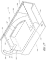
- a photovoltaic assembly 100 for converting solar radiation to electrical energy is shown.
- the photovoltaic assembly 100 can have a photovoltaic module 110 similar to the photovoltaic assembly 110 described in association with FIG. 1 .
- the photovoltaic assembly 100 also has an electronic component housing 120 coupled to the backsheet 119.
- a photovoltaic module 110 is shown in FIG. 2 , the photovoltaic assembly 110 can alternatively include a photovoltaic concentrator and an electronic component housing in another embodiment.
- FIG. 3 illustrates a schematic perspective view of the electronic component housing 120 described in FIG. 2 .
- the electronic component housing 120 has an upper portion 122, a middle portion 124 and a lower portion 126.
- the upper portion is coupled to the back side 114 of the photovoltaic module 110 on the backsheet 119.
- FIG. 3 depicts one exemplary arrangement of elements, additional intervening elements, devices, features, or components can be present in one or more embodiments of the present invention.
- the middle portion 124 of the electronic component housing 120 includes an opening 130 which can be a through-hole, an opening on one end which extends through to the other end of the electronic component housing 120.
- the opening 130 can permit heat transfer between the heat sink 127 and the ambient environment.
- the ambient environment is the open air above and below the photovoltaic module 110.
- the opening 130 can also allow for air flow between the laminate 116 and electronic components housed in the electronic component housing 120, effectively cooling the electronic component housing 120 and allowing heat to escape.
- An electronic cable 129 can be included and used for outputting electricity produced by the photovoltaic assembly 100.
- the heat sink 127 is a device which receives, directs, and spreads thermal energy.
- the heat sink 127 can be composed of a material with high thermal conductivity, such as copper, aluminum, or another metal. It can also be composed of a material not well-known for thermal conductivity if the other material is more suitable for other reasons like cost, availability, dielectric properties, or other design constraints in the electronic component housing 120.
- the heat sink 127 thermally communicates directly with the electronic component 128 and, in some embodiments, can be integrally formed with the electronic component housing 120. It can distribute and exchange heat through its surface features and geometric shape. Such shapes and features can include fins of any type, size, or arrangement, including planar elements, cylindrical extensions, and so on.
- the fins of a heat sink can be referred to as air fins herein, although they are integrally formed with other components of the heat sink 127.
- the fins can direct air flow, in addition to increasing the rate of heat transfer from the heat sink 127 to the environment.
- the heat sink 127 can have fins disposed between two rectangular prisms, projecting from one or several surfaces, and other configurations. The planar surface of the fins can be aligned to expected airflow or perpendicular to it, or any intermediate configuration.
- the electronic component housing 120 is composed of aluminum. In another embodiment, the electronic component housing 120 is composed of a heat dissipating polymer. In an embodiment, the backsheet 119 of the photovoltaic module 110 is fabricated from a glass or a plastic polymer.
- the electronic component housing 120 is mounted on the corner of the photovoltaic module 110
- the electronic component housing 120 can be mounted at other suitable locations, such as a location anywhere at the back side 114 of the photovoltaic module 110.
- the electronic component housing 120 can be mounted directly and solely to the backside 114 of the photovoltaic laminate 116, such as mounted to the backsheet 119.
- illustrated embodiments comprise frame 118
- the frame 118 can be omitted and the photovoltaic laminate 116 can be supported by non-frame elements while still including the improved electronic component housing described herein.
- the electronic component housing 120 can be additionally coupled to the frame 118 along one or several sides of the housing 120 or frame 118.
- the electronic component housing 120 has an upper portion 122, middle portion 124 and lower portion 126.
- the upper portion is coupled to the back side 114 of the photovoltaic module 110 through the backsheet 119.
- the middle portion can include a heat sink 127 and an opening 130.
- the lower portion 126 encloses an electronic component 128.
- the electric component 128 can be distributed partially or entirely in either or both of the upper and lower 122, 126 portions of the electronic component housing 120.
- the electronic component 128 can be a microinverter which can be used to convert the output current of the photovoltaic assembly 100 from direct current (DC) to alternating current (AC) and outputting AC, since most homes and facilities use AC.
- the electronic component 128 includes a junction box or the electronic components of a photovoltaic module junction box.
- the electronic component 128 includes a DC to DC optimizer or other distributed power conditioning electronic device.
- a thermally-conductive adhesive 125 is placed between the backsheet 119 and the upper portion 122 of the electronic component housing 120, as depicted in FIG. 5 .
- the thermally-conductive adhesive 125 can be provided to keep the electronic component housing 120 secured to the backsheet 119.
- the thermally-conductive adhesive 125 is used to absorb and/or transfer heat from the backsheet 119 so that heat is transported from either or both of the backsheet 119 and the electronic component housing 120, though not necessarily in even amounts, to the environment through the heat sink 127.
- the adhesive can have relatively higher thermal insulation characteristics, and can be used to insulate the photovoltaic module 110 from heat generated in the electronic component housing 120.
- damage caused by heat transferred from the electronic component housing 120 and travelling into the photovoltaic laminate 116 is inhibited.
- FIG. 6 a schematic cross-sectional diagram for another embodiment of a photovoltaic assembly 200 is shown.
- the numeric indicators used to refer to components in FIGS. 1-5 are similar to the components in FIGS. 6-20 , except that the index has been incremented in increasing units of 100.
- the photovoltaic assembly 200 includes a photovoltaic module 210 having a front side 212, a back side 214, a frame, a laminate 216, a plurality of solar cells 217 and a backsheet 219.
- the electronic component housing 220 has an upper portion 222 coupled to the the backsheet 119 and a lower portion 226 enclosing an electronic component.
- the middle portion 224 of the electronic component housing 220 includes a first opening 232 and a second opening 234.
- an electronic component can be disposed between the first opening 232 and the second opening 234 or distributed within the upper, middle, and lower portions 222, 224, 226 of the electronic component housing.
- additional openings can be included, possibly defining additional regions for disposing an electronic component.
- FIG. 7 illustrates a schematic perspective view of the photovoltaic assembly 200.
- a frame 218 is depicted, along with backsheet 219 and electronic component housing 220.
- the upper portion 222, middle portion 224 and lower portion 226 of the electronic component housing 220 enclosing an electronic component are also shown.
- the first 232 and second openings 234 are included in the middle portion 224 of the electronic component housing 220.
- FIG. 8 a schematic cross-sectional diagram for another embodiment of a photovoltaic assembly 300 is shown.
- Photovoltaic assembly 300 is similar to the assemblies described in association with FIGS. 1-5 , with the addition of air fins 339 disposed within the heat sink 327 found in the middle portion 324 of the electronic component housing 320.
- the air fins 339 extend from the lower portion 326 to contact the upper portion 322.
- the air fins 339 allow additional paths for air flow and fluid thermal communication between the heat sink 327 and an ambient environment.
- the air fins 339 also promote and contribute to cooling of the electronic component housing 320 as described above.
- the air fins 339 can extend only partially between the upper and lower portions 322, 324, and thus only partially across the middle portion 324. In such embodiments, the air fins 339 do not contact the upper portion 322.
- FIG. 9 illustrates a schematic perspective view of the photovoltaic assembly 300 described in association FIG. 8 , wherein the air fins 339 within the middle portion 324 are shown.
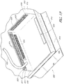
- FIG. 10 a perspective view for yet another embodiment of a photovoltaic assembly 300 is shown.
- the photovoltaic assembly 300 depicted in FIG. 10 is similar to the assemblies described in association with FIG. 8 , with the exception that the middle portion 324 includes of air fins 339 within an opening 830 along all sides of the electronic component housing 320.
- the air fins 339 can act as heat-directing channels from the heat sink 327 to an ambient environment, as described above.
- the opening 830 can also be present on any number of sides of the electronic component housing 320, whether one, all, or any number in between. Additionally, numerous smaller openings can be substituted for opening 830, resulting in a grill, mesh, or series of ports opening in the side of the electronic component housing 320.
- FIG. 11 a schematic cross-sectional diagram for still another embodiment of a photovoltaic assembly 400 is depicted.
- the photovoltaic assembly 400 shown in FIG. 11 is similar to the assemblies described in association with FIGS. 8-10 .
- an electronic component housing 420 has an opening 430 with air fins 439 which extend from the surface of the heat sink 427 toward the upper portion 422 of the electronic component housing 420 without touching the upper portion 422.
- FIG. 12 illustrates a schematic perspective view for an embodiment of the photovoltaic assembly 400.
- the air fins 439 are depicted as positioned in the opening 430.
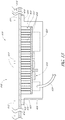
- the photovoltaic assembly 500 includes an upper portion 522 having an L-shaped structure 550 extending from the lower portion 526 of an electronic component housing 520 and bending inward to couple to a backsheet 519 of a photovoltaic module 510.
- the middle portion 524 of the electronic component housing 520 can include a first set of air fins 539 and a second set of air fins 542 disposed within a heat sink 527 positioned in an opening 530,.
- the second set of air fins 542 extends from the lower portion 526 of the electronic component housing 520 to contact the backsheet 519, between the L-shaped structure 550, allowing for heat to transfer from the backsheet 519 to the heat sink 527. Due to the L-shaped structure 550 extending from the lower 526 portion and bending inward, the first set of air fins 539 extends without touching the backsheet 519. Although in some embodiments, such as the illustrated embodiment, the first set of air fins 539 does not contact the L-shaped structures 550, in other embodiments, the first set of air fins 539 can contact the L-shaped structure 550.
- the L-shaped structure 550 can, in some embodiments, be constructed to permit effective thermal communication between the backsheet 519 and the first set of air fins 539.
- FIG. 14 illustrates a schematic perspective view of the photovoltaic assembly 500 described in association with FIG. 13 .
- the L-shaped structure 550 of the upper portion 522, the middle portion 524 with the first and second sets of air fins 540 and 542 in the opening 530, and the lower portion 526 are shown.
- FIG. 15 a schematic cross-sectional diagram for another embodiment of a photovoltaic assembly 600 is shown.
- the photovoltaic assembly 600 is similar to the assemblies described in association with FIGS. 13 and 14 .
- the upper portion 622 of an electronic component housing 620 has an L-shaped structure 650 extending from the lower portion 626 but, in contrast to the above described assembly, the L-shaped structure 650 bends outward to couple to a backsheet 619 of a photovoltaic module 610.
- the air fins 639 extend from the lower portion 626 to contact the backsheet 619. In one such embodiment, in an opening 630, at least one of the air fins 639 contacts the backsheet 619 to facilitate thermal communication between the backsheet and a heat sink 627, as depicted in FIG. 15 .
- FIG. 16 illustrates a schematic perspective view for the photovoltaic assembly 600 described in association with FIG. 15 .
- the L-shaped structure 650, the middle portion 624 having air fins 639 extending and touching the backsheet 619, and the lower portion 626 are shown.
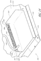
- FIG. 17 a cross sectional and schematic perspective view for still another embodiment of a photovoltaic assembly 700 is shown.
- the photovoltaic assembly 700 is similar to the assemblies described in association with FIGS. 1-5 .
- the middle portion 724 of an electronic component housing 720 has a first opening 732 originating between the upper portion 722 and lower portion 726 of the electronic component housing 720 and ending in a second opening 734 disposed between the upper portion 722 and lower portion 726 of the electronic component housing 720.
- a conduit 738 extends between the first and second openings 732, 734, and can include, as one wall of the conduit 738, at least a portion of the heat sink 727. Thus, heat exchange can occur between the heat sink 727 and air flowing through the conduit 738.
- the conduit 738 is curved, as depicted in FIG. 17 .
- the middle portion 724 can include a curved heat sink 727.
- air fins can extend from the heat sink 727 into the conduit 738, as well.
- at least one of the first opening 732, second opening 734, and the conduit 738 can include a fan or other forced air mechanism to direct air through the conduit 738 in a desired direction.
- the conduit can split off into multiple conduits that can require any number of additional openings.
- FIG. 18 illustrates a schematic perspective view for the photovoltaic assembly 700.
- the electronic component housing 720 includes an upper portion 722 coupled to the backsheet 719, a middle portion 724 and a lower portion 726.
- the middle portion 724 has a first opening 732 and the lower section 726 has a second opening 734.
- the conduit 738 extends between the first and second openings 732, 734.
- FIG. 19 a schematic perspective view for yet another embodiment of a photovoltaic assembly 800 is shown.
- the photovoltaic assembly 800 is representative of a combination of the assemblies described in association with FIGS. 10 , 17 and 18 .
- the electronic component housing 820 has an upper section 822 coupled to a backsheet 819, a middle section 824 and a lower section 826.
- the electronic component housing 820 has a plurality of air fins 839 extending from the heat sink 827 and protruding into airspace communicating with opening 830 in the middle section 824.
- the lower section 826 has a first opening 834 from the area of the electronic component housing 820 perpendicular to the backsheet 819, and a second opening 836 on the area parallel to the backsheet 819.
- FIG. 20 illustrates a schematic perspective cross-sectional view for the photovoltaic assembly 800. This view shows a diagonal air channel or conduit 838 allowing the first opening 834 and second opening 836 to be connected with the air fins 839.
- a diagonal channel is curved similar to the assemblies described in association with FIGS. 17 and 18 .
- the photovoltaic assembly 800 provides an active cooling system mounted on the first opening 836, second opening 834 or opening 830. The active cooling system can be used to direct air into or out from the electronic component housing 820.
Description
- Embodiments of the subject matter described herein relate generally to photovoltaic assemblies including solar cells, photovoltaic modules and associated electronic components. More particularly, one or more embodiments of the present invention relate to photovoltaic modules, electronic housing components and heat sinks.
-
JP H11 251614 A EP 0 793 278 A2JP 2007 166721 A FR 2 914 754 A1 - Solar cells are well known devices for converting solar radiation to electrical energy. Several solar cells can be connected to together to form a solar cell array. The solar cell array can be packaged into a photovoltaic (PV) module using various processes and encapsulant materials. Electronic components and wiring are required to convert, gather and transfer generated electric current. These electronic components are usually mounted close to the back of a photovoltaic module so that shipping density of the photovoltaic modules is not compromised. During operation, the electronic components can generate or trap heat which can cause the encapsulant materials to degrade at an accelerated rate. The heat can also permanently damage the cells inside photovoltaic module, or cause temporary performance degradation. One or more embodiments of the present invention pertain to photovoltaic assemblies that present alternative means of transferring heat from the electronics components to an ambient environment.
- A more complete understanding of the subject matter can be derived by referring to the detailed description when considered in conjunction with the following figures, wherein like reference numbers refer to similar elements throughout the figures.
-
FIG. 1 is a schematic perspective view of a photovoltaic module in accordance with an embodiment of the present invention; -
FIG. 2 is a schematic perspective view of a photovoltaic assembly in accordance with an embodiment; -
FIG. 3 is a schematic perspective view of the electronic component housing ofFIG. 2 in accordance with an embodiment; -
FIG. 4 is a schematic cross-sectional diagram of the electronic component housing ofFIG. 3 in accordance with an embodiment; -
FIG. 5 is a schematic cross-sectional diagram of a photovoltaic assembly in accordance with yet another embodiment; -
FIG. 6 is a schematic cross-sectional diagram of a photovoltaic assembly in accordance with still another embodiment; -
FIG. 7 is a schematic perspective view of the photovoltaic assembly ofFIG. 6 in accordance with still another embodiment; -
FIG. 8 is a schematic cross-sectional diagram of a photovoltaic assembly in accordance with yet another embodiment; -
FIG. 9 is a schematic perspective view of the photovoltaic assembly ofFIG. 8 in accordance with yet another embodiment; -
FIG. 10 is a schematic perspective view of a photovoltaic assembly in accordance with another embodiment; -
FIG. 11 is a schematic cross-sectional diagram of a photovoltaic assembly in accordance with still another embodiment; -
FIG. 12 is a schematic perspective view of the photovoltaic assembly ofFIG. 11 in accordance with still another embodiment; -
FIG. 13 is a schematic cross-sectional diagram of a photovoltaic assembly in accordance with another embodiment; -
FIG. 14 is a schematic perspective view of the photovoltaic assembly ofFIG. 13 in accordance with another embodiment; -
FIG. 15 is a schematic cross-sectional diagram of a photovoltaic assembly in accordance with yet another embodiment; -
FIG. 16 is a schematic perspective view of the photovoltaic assembly ofFIG. 15 in accordance with yet another embodiment; -
FIG. 17 is a schematic perspective view of a photovoltaic assembly in accordance with still another embodiment; -
FIG. 18 is a schematic perspective view of the photovoltaic assembly ofFIG. 17 in accordance with still another embodiment; -
FIG. 19 is a schematic perspective view of a photovoltaic assembly in accordance with another embodiment; -
FIG. 20 is a schematic cross-sectional diagram of the photovoltaic assembly ofFIG. 19 in accordance with another embodiment; - The following detailed description is merely illustrative in nature and is not intended to limit the embodiments of the subject matter or the application and uses of such embodiments. As used herein, the word "exemplary" means "serving as an example, instance, or illustration." Any implementation described herein as exemplary is not necessarily to be construed as preferred or advantageous over other implementations. Furthermore, there is no intention to be bound by any expressed or implied theory presented in the preceding technical field, background, brief summary or the following detailed description.
- In addition, certain terminology can also be used in the following description for the purpose of reference only, and thus is not intended to be limiting. For example, terms such as "upper", "middle", and "lower" refer to directions in the drawings to which reference is made. Terms such as "front" and "back" describe the orientation and/or location of portions of the component within a consistent but arbitrary frame of reference which is made clear by reference to the text and the associated drawings describing the component under discussion. Such terminology can include the words specifically mentioned above, derivatives thereof, and words of similar import. Similarly, the terms "first", "second", and other such numerical terms referring to structures do not imply a sequence or order unless clearly indicated by the context.
- "Inhibit" - As used herein, inhibit is used to describe a reducing or minimizing effect. When a component or feature is described as inhibiting an action, motion, or condition it may completely prevent the result or outcome or future state completely. Additionally, "inhibit" can also refer to a reduction or lessening of the outcome, performance, and/or effect which might otherwise occur. Accordingly, when a component, element, or feature is referred to as inhibiting a result or state, it need not completely prevent or eliminate the result or state.
- A photovoltaic assembly for converting solar radiation to electrical energy is defined in claim 1. Further advantageous embodiments are defined in the dependent claims.
- As used herein, unless expressly stated otherwise, "coupled" means that one element/node/feature is directly or indirectly joined to (or directly or indirectly communicates with) another element/node/feature, and not necessarily mechanically coupled.
-
FIGS. 1-20 illustrate various embodiments of a photovoltaic assembly for converting solar radiation to electrical energy. Numerous specific details are provided, such as examples of apparatuses and components to provide a thorough understanding of at least some embodiments of the present invention. It is to be understood, however, that other embodiments of the present invention can be practiced without one or more of the specific details set forth. In other instances, well-known details are not shown or described in order to avoid obscuring aspects of certain embodiments of the present invention. -
FIG. 1 illustrates aphotovoltaic module 110 having afront side 112 that faces the sun during normal operation and aback side 114 opposite thefront side 112. In some embodiments, thephotovoltaic module 110 has aframe 118 and alaminate 116 containing a plurality ofsolar cells 117. Thesolar cells 117 face thefront side 112. Thelaminate 116 can include one or moreencapsulating layers 111 which surround and enclose thesolar cells 117. Acover 115 made of glass or another transparent material can be laminated to theencapsulant layers 111. In certain embodiments, the material chosen for construction of thecover 115 can be selected for properties which minimize reflection, thereby permitting the maximum amount of sunlight to reach thesolar cells 117. Thecover 115 can provide structural rigidity to thelaminate 116. The laminate 116 can also have abacksheet 119. Thebacksheet 119 can be a weatherproof and electrically insulating layer which protects the underside of the laminate 116. Thebacksheet 119 can be a polymer sheet, and it can be laminated to the encapsulant layer(s) 111 of the laminate 116, or it can be integral with one of the layers of theencapsulant 111. - With reference to
FIG. 2 , aphotovoltaic assembly 100 for converting solar radiation to electrical energy is shown. Thephotovoltaic assembly 100 can have aphotovoltaic module 110 similar to thephotovoltaic assembly 110 described in association withFIG. 1 . Thephotovoltaic assembly 100 also has anelectronic component housing 120 coupled to thebacksheet 119. Although aphotovoltaic module 110 is shown inFIG. 2 , thephotovoltaic assembly 110 can alternatively include a photovoltaic concentrator and an electronic component housing in another embodiment. -
FIG. 3 illustrates a schematic perspective view of theelectronic component housing 120 described inFIG. 2 . Theelectronic component housing 120 has anupper portion 122, amiddle portion 124 and alower portion 126. The upper portion is coupled to theback side 114 of thephotovoltaic module 110 on thebacksheet 119. Although the schematic shown inFIG. 3 depicts one exemplary arrangement of elements, additional intervening elements, devices, features, or components can be present in one or more embodiments of the present invention. - With additional reference to
FIG. 4 , themiddle portion 124 of theelectronic component housing 120 includes anopening 130 which can be a through-hole, an opening on one end which extends through to the other end of theelectronic component housing 120. Theopening 130 can permit heat transfer between theheat sink 127 and the ambient environment. The ambient environment is the open air above and below thephotovoltaic module 110. Theopening 130 can also allow for air flow between the laminate 116 and electronic components housed in theelectronic component housing 120, effectively cooling theelectronic component housing 120 and allowing heat to escape. Anelectronic cable 129 can be included and used for outputting electricity produced by thephotovoltaic assembly 100. - The
heat sink 127 is a device which receives, directs, and spreads thermal energy. Theheat sink 127 can be composed of a material with high thermal conductivity, such as copper, aluminum, or another metal. It can also be composed of a material not well-known for thermal conductivity if the other material is more suitable for other reasons like cost, availability, dielectric properties, or other design constraints in theelectronic component housing 120. Theheat sink 127 thermally communicates directly with theelectronic component 128 and, in some embodiments, can be integrally formed with theelectronic component housing 120. It can distribute and exchange heat through its surface features and geometric shape. Such shapes and features can include fins of any type, size, or arrangement, including planar elements, cylindrical extensions, and so on. The fins of a heat sink can be referred to as air fins herein, although they are integrally formed with other components of theheat sink 127. The fins can direct air flow, in addition to increasing the rate of heat transfer from theheat sink 127 to the environment. Theheat sink 127 can have fins disposed between two rectangular prisms, projecting from one or several surfaces, and other configurations. The planar surface of the fins can be aligned to expected airflow or perpendicular to it, or any intermediate configuration. - In an embodiment, the
electronic component housing 120 is composed of aluminum. In another embodiment, theelectronic component housing 120 is composed of a heat dissipating polymer. In an embodiment, thebacksheet 119 of thephotovoltaic module 110 is fabricated from a glass or a plastic polymer. - Although it is shown in
FIG. 2 that theelectronic component housing 120 is mounted on the corner of thephotovoltaic module 110, theelectronic component housing 120 can be mounted at other suitable locations, such as a location anywhere at theback side 114 of thephotovoltaic module 110. Theelectronic component housing 120 can be mounted directly and solely to thebackside 114 of thephotovoltaic laminate 116, such as mounted to thebacksheet 119. Thus, although illustrated embodiments compriseframe 118, in other embodiments, theframe 118 can be omitted and thephotovoltaic laminate 116 can be supported by non-frame elements while still including the improved electronic component housing described herein. In those embodiments comprising a frame, theelectronic component housing 120 can be additionally coupled to theframe 118 along one or several sides of thehousing 120 orframe 118. - With continued reference to
FIG. 4 and additional reference toFIG. 5 , schematic cross-sectional diagrams of thephotovoltaic assembly 100 are shown. Theelectronic component housing 120 has anupper portion 122,middle portion 124 andlower portion 126. The upper portion is coupled to theback side 114 of thephotovoltaic module 110 through thebacksheet 119. The middle portion can include aheat sink 127 and anopening 130. Thelower portion 126 encloses anelectronic component 128. Alternatively, theelectric component 128 can be distributed partially or entirely in either or both of the upper and lower 122, 126 portions of theelectronic component housing 120. Thus, that at least some of the constituent elements of theelectronic component 128 can be present in any of the upper, middle, orlower portions electronic component housing 120. Theheat sink 127 can also be on the upper, lower, or both upper and lower portion of theopening 130. Theelectronic component 128 can be a microinverter which can be used to convert the output current of thephotovoltaic assembly 100 from direct current (DC) to alternating current (AC) and outputting AC, since most homes and facilities use AC. In another embodiment, theelectronic component 128 includes a junction box or the electronic components of a photovoltaic module junction box. In yet another embodiment, theelectronic component 128 includes a DC to DC optimizer or other distributed power conditioning electronic device. - In yet another embodiment, a thermally-
conductive adhesive 125 is placed between thebacksheet 119 and theupper portion 122 of theelectronic component housing 120, as depicted inFIG. 5 . The thermally-conductive adhesive 125 can be provided to keep theelectronic component housing 120 secured to thebacksheet 119. In one embodiment, the thermally-conductive adhesive 125 is used to absorb and/or transfer heat from thebacksheet 119 so that heat is transported from either or both of thebacksheet 119 and theelectronic component housing 120, though not necessarily in even amounts, to the environment through theheat sink 127.. In another embodiment the adhesive can have relatively higher thermal insulation characteristics, and can be used to insulate thephotovoltaic module 110 from heat generated in theelectronic component housing 120. Advantageously, damage caused by heat transferred from theelectronic component housing 120 and travelling into thephotovoltaic laminate 116 is inhibited. - With reference to
FIG. 6 , a schematic cross-sectional diagram for another embodiment of aphotovoltaic assembly 200 is shown. Unless otherwise specified below, the numeric indicators used to refer to components inFIGS. 1-5 are similar to the components inFIGS. 6-20 , except that the index has been incremented in increasing units of 100. - Similar to
FIGS. 1-5 , thephotovoltaic assembly 200 includes aphotovoltaic module 210 having afront side 212, aback side 214, a frame, a laminate 216, a plurality ofsolar cells 217 and abacksheet 219. Theelectronic component housing 220 has anupper portion 222 coupled to the thebacksheet 119 and alower portion 226 enclosing an electronic component. Themiddle portion 224 of theelectronic component housing 220 includes afirst opening 232 and asecond opening 234. Although not shown, an electronic component can be disposed between thefirst opening 232 and thesecond opening 234 or distributed within the upper, middle, andlower portions -
FIG. 7 illustrates a schematic perspective view of thephotovoltaic assembly 200. Aframe 218 is depicted, along withbacksheet 219 andelectronic component housing 220. Theupper portion 222,middle portion 224 andlower portion 226 of theelectronic component housing 220 enclosing an electronic component are also shown. The first 232 andsecond openings 234 are included in themiddle portion 224 of theelectronic component housing 220. - With reference to
FIG. 8 , a schematic cross-sectional diagram for another embodiment of aphotovoltaic assembly 300 is shown.Photovoltaic assembly 300 is similar to the assemblies described in association withFIGS. 1-5 , with the addition ofair fins 339 disposed within theheat sink 327 found in themiddle portion 324 of theelectronic component housing 320. In one embodiment, theair fins 339 extend from thelower portion 326 to contact theupper portion 322. In one such embodiment, theair fins 339 allow additional paths for air flow and fluid thermal communication between theheat sink 327 and an ambient environment. Theair fins 339 also promote and contribute to cooling of theelectronic component housing 320 as described above. In certain embodiments, theair fins 339 can extend only partially between the upper andlower portions middle portion 324. In such embodiments, theair fins 339 do not contact theupper portion 322. -
FIG. 9 illustrates a schematic perspective view of thephotovoltaic assembly 300 described in associationFIG. 8 , wherein theair fins 339 within themiddle portion 324 are shown. - With reference to
FIG. 10 , a perspective view for yet another embodiment of aphotovoltaic assembly 300 is shown. Referring to the above, thephotovoltaic assembly 300 depicted inFIG. 10 is similar to the assemblies described in association withFIG. 8 , with the exception that themiddle portion 324 includes ofair fins 339 within anopening 830 along all sides of theelectronic component housing 320. Theair fins 339 can act as heat-directing channels from theheat sink 327 to an ambient environment, as described above. Theopening 830 can also be present on any number of sides of theelectronic component housing 320, whether one, all, or any number in between. Additionally, numerous smaller openings can be substituted for opening 830, resulting in a grill, mesh, or series of ports opening in the side of theelectronic component housing 320. - With reference to
FIG. 11 , a schematic cross-sectional diagram for still another embodiment of aphotovoltaic assembly 400 is depicted. Thephotovoltaic assembly 400 shown inFIG. 11 is similar to the assemblies described in association withFIGS. 8-10 . However, anelectronic component housing 420 has anopening 430 withair fins 439 which extend from the surface of theheat sink 427 toward theupper portion 422 of theelectronic component housing 420 without touching theupper portion 422. -
FIG. 12 illustrates a schematic perspective view for an embodiment of thephotovoltaic assembly 400. Theair fins 439 are depicted as positioned in theopening 430. - With reference to
FIG. 13 , a schematic cross-sectional diagram for yet another embodiment of aphotovoltaic assembly 500 is shown. Thephotovoltaic assembly 500 includes anupper portion 522 having an L-shapedstructure 550 extending from thelower portion 526 of anelectronic component housing 520 and bending inward to couple to abacksheet 519 of aphotovoltaic module 510. Themiddle portion 524 of theelectronic component housing 520 can include a first set ofair fins 539 and a second set ofair fins 542 disposed within aheat sink 527 positioned in anopening 530,. In an embodiment, the second set ofair fins 542 extends from thelower portion 526 of theelectronic component housing 520 to contact thebacksheet 519, between the L-shapedstructure 550, allowing for heat to transfer from thebacksheet 519 to theheat sink 527. Due to the L-shapedstructure 550 extending from the lower 526 portion and bending inward, the first set ofair fins 539 extends without touching thebacksheet 519. Although in some embodiments, such as the illustrated embodiment, the first set ofair fins 539 does not contact the L-shapedstructures 550, in other embodiments, the first set ofair fins 539 can contact the L-shapedstructure 550. The L-shapedstructure 550 can, in some embodiments, be constructed to permit effective thermal communication between thebacksheet 519 and the first set ofair fins 539. -
FIG. 14 illustrates a schematic perspective view of thephotovoltaic assembly 500 described in association withFIG. 13 . The L-shapedstructure 550 of theupper portion 522, themiddle portion 524 with the first and second sets ofair fins opening 530, and thelower portion 526 are shown. - With reference to
FIG. 15 , a schematic cross-sectional diagram for another embodiment of aphotovoltaic assembly 600 is shown. Thephotovoltaic assembly 600 is similar to the assemblies described in association withFIGS. 13 and14 . Theupper portion 622 of anelectronic component housing 620 has an L-shapedstructure 650 extending from thelower portion 626 but, in contrast to the above described assembly, the L-shapedstructure 650 bends outward to couple to abacksheet 619 of aphotovoltaic module 610. Theair fins 639 extend from thelower portion 626 to contact thebacksheet 619. In one such embodiment, in anopening 630, at least one of theair fins 639 contacts thebacksheet 619 to facilitate thermal communication between the backsheet and aheat sink 627, as depicted inFIG. 15 . -
FIG. 16 illustrates a schematic perspective view for thephotovoltaic assembly 600 described in association withFIG. 15 . The L-shapedstructure 650, themiddle portion 624 havingair fins 639 extending and touching thebacksheet 619, and thelower portion 626 are shown. - With reference to
FIG. 17 , a cross sectional and schematic perspective view for still another embodiment of aphotovoltaic assembly 700 is shown. Thephotovoltaic assembly 700 is similar to the assemblies described in association withFIGS. 1-5 . However, themiddle portion 724 of anelectronic component housing 720 has afirst opening 732 originating between theupper portion 722 andlower portion 726 of theelectronic component housing 720 and ending in asecond opening 734 disposed between theupper portion 722 andlower portion 726 of theelectronic component housing 720. Aconduit 738 extends between the first andsecond openings conduit 738, at least a portion of theheat sink 727. Thus, heat exchange can occur between theheat sink 727 and air flowing through theconduit 738. This arrangement is in contrast to the assemblies described in association withFIGS. 1-5 wherein the opening is through-hole only. In an embodiment, theconduit 738 is curved, as depicted inFIG. 17 . In some embodiments, including the illustrated embodiment, themiddle portion 724 can include acurved heat sink 727. In some embodiments, air fins can extend from theheat sink 727 into theconduit 738, as well. In certain embodiments, at least one of thefirst opening 732,second opening 734, and theconduit 738 can include a fan or other forced air mechanism to direct air through theconduit 738 in a desired direction. In yet another embodiment, the conduit can split off into multiple conduits that can require any number of additional openings. -
FIG. 18 illustrates a schematic perspective view for thephotovoltaic assembly 700. Theelectronic component housing 720 includes anupper portion 722 coupled to thebacksheet 719, amiddle portion 724 and alower portion 726. Themiddle portion 724 has afirst opening 732 and thelower section 726 has asecond opening 734. Theconduit 738 extends between the first andsecond openings - With reference to
FIG. 19 , a schematic perspective view for yet another embodiment of aphotovoltaic assembly 800 is shown. Thephotovoltaic assembly 800 is representative of a combination of the assemblies described in association withFIGS. 10 ,17 and18 . Theelectronic component housing 820 has anupper section 822 coupled to abacksheet 819, amiddle section 824 and alower section 826. Theelectronic component housing 820 has a plurality ofair fins 839 extending from the heat sink 827 and protruding into airspace communicating withopening 830 in themiddle section 824. Thelower section 826 has afirst opening 834 from the area of theelectronic component housing 820 perpendicular to thebacksheet 819, and asecond opening 836 on the area parallel to thebacksheet 819. -
FIG. 20 illustrates a schematic perspective cross-sectional view for thephotovoltaic assembly 800. This view shows a diagonal air channel orconduit 838 allowing thefirst opening 834 andsecond opening 836 to be connected with theair fins 839. - In an alternative embodiment, a diagonal channel is curved similar to the assemblies described in association with
FIGS. 17 and18 . In another embodiment, thephotovoltaic assembly 800 provides an active cooling system mounted on thefirst opening 836,second opening 834 oropening 830. The active cooling system can be used to direct air into or out from theelectronic component housing 820.
Claims (16)
- A photovoltaic assembly comprising:a photovoltaic module (110, 210, 310, 410, 510, 610, 710) having a front side (112, 212, 312, 412, 512, 612) that faces the sun during normal operation and a back side (114, 214, 314, 414, 514, 614) opposite the front side, the photovoltaic module comprising:a plurality of solar cells (117, 217, 317, 417, 517, 617) on the front side disposed within the photovoltaic module; anda backsheet (119, 219, 319, 419, 519, 619, 719, 819) on the back side of the photovoltaic module; andan electronic component housing (120, 220, 320, 420, 520, 620, 720, 820) comprising:an upper portion (122, 222, 322, 422, 522, 622, 722, 822) coupled to the backsheet of the photovoltaic module;a lower portion (126, 226, 326, 426, 526, 626, 726, 826) enclosing an electronic component (128, 228, 328, 428, 528, 628); anda middle portion (124, 224, 324, 424, 524, 624, 724, 824) comprising:a heat sink (127, 227, 327, 427, 527, 627, 727, 827) in thermal communication with the electronic component;an opening (130, 232, 234, 330, 430, 530, 630, 732, 734, 830, 834, 836) in the electronic component housing between the upper portion and lower portion, the opening permitting fluid communication between the heat sink and an ambient environment; andcharacterized by a plurality of air fins (339, 439, 539, 639, 839) distributed within the opening in the electronic component housing.
- The photovoltaic assembly according to claim 1, wherein the opening (130, 232, 234, 330, 430, 530, 630, 732, 734, 830, 834, 836) originates from the lower portion and ends in between the upper portion and lower portion.
- The photovoltaic assembly of Claim 1 or 2, wherein the electronic component (128, 228, 328, 428, 528, 628) comprises a microinverter for converting direct current generated from the solar module into alternating current and outputting alternating current.
- The photovoltaic assembly of Claim 1 or 2, wherein the electronic component (128, 228, 328, 428, 528, 628) comprises an electronic junction box.
- The photovoltaic assembly of any one of Claims 1 to 4, further comprising a heat conductive adhesive (125) between the upper section of the electronic component housing and the backsheet.
- The photovoltaic assembly of any one of Claims 1 to 5, wherein the electronic component (128, 228, 328, 428, 528, 628) is distributed within the middle portion of the electronic component housing.
- The photovoltaic assembly of Claim 1 or 2, wherein the electronic component (128, 228, 328, 428, 528, 628) comprises an electronic DC to DC optimizer.
- The photovoltaic assembly of any one of Claims 1 to 7, wherein the opening is a plurality of openings (232, 234, 732, 734, 830, 834, 836).
- The photovoltaic assembly of Claim 8, wherein the plurality of air fins (339, 439, 539, 639, 839) is distributed within the plurality of openings.
- The photovoltaic assembly of any one of Claims 1 to 9, wherein the electronic component housing (120, 220, 320, 420, 520, 620, 720, 820) comprises aluminum or a heat dissipating polymer.
- The photovoltaic assembly of any one of Claims 1 to 10, wherein the backsheet (119, 219, 319, 419, 519, 619, 719, 819) of the photovoltaic module comprises a glass or a plastic polymer.
- The photovoltaic assembly of any one of Claims 1 to 11, wherein the photovoltaic module (110, 210, 310, 410, 510, 610, 710) comprises a photovoltaic concentrator.
- The photovoltaic assembly of any one of Claims 1 to 12, wherein the upper portion (522, 622) comprises an L-shaped structure (550, 650) extending from the lower portion and bending inward to couple to the backsheet of the photovoltaic module.
- The photovoltaic assembly of Claim 13, wherein the upper portion (522, 622) comprising the L-shaped structure (550, 650) extending from the lower portion and bending inward comprises an L-shaped structure extending from the lower portion and bending outward to couple to the backsheet of the photovoltaic module.
- The photovoltaic assembly of claim 8, wherein the plurality of openings has a first opening (732) and a second opening (734), the first opening originating between the upper portion (722) and lower portion (726) and ending in the second opening (734) disposed between the upper portion (722) and lower portion (726),
further comprising a conduit (738) extending between the first opening (732) and the second opening (734). - The photovoltaic assembly of claim 15, wherein at least a portion of the heat sink (727) serves as one wall of the conduit (738).
Applications Claiming Priority (2)
| Application Number | Priority Date | Filing Date | Title |
|---|---|---|---|
| US13/436,723 US9635783B2 (en) | 2012-03-30 | 2012-03-30 | Electronic component housing with heat sink |
| PCT/US2013/033797 WO2013148624A2 (en) | 2012-03-30 | 2013-03-26 | Electronic component housing with heat sink |
Publications (3)
| Publication Number | Publication Date |
|---|---|
| EP2831925A2 EP2831925A2 (en) | 2015-02-04 |
| EP2831925A4 EP2831925A4 (en) | 2015-04-08 |
| EP2831925B1 true EP2831925B1 (en) | 2017-07-19 |
Family
ID=49233241
Family Applications (1)
| Application Number | Title | Priority Date | Filing Date |
|---|---|---|---|
| EP13768875.0A Not-in-force EP2831925B1 (en) | 2012-03-30 | 2013-03-26 | Electronic component housing with heat sink |
Country Status (6)
| Country | Link |
|---|---|
| US (1) | US9635783B2 (en) |
| EP (1) | EP2831925B1 (en) |
| JP (1) | JP6209790B2 (en) |
| KR (1) | KR20140147869A (en) |
| AU (1) | AU2013239955B2 (en) |
| WO (1) | WO2013148624A2 (en) |
Families Citing this family (19)
| Publication number | Priority date | Publication date | Assignee | Title |
|---|---|---|---|---|
| KR102272506B1 (en) * | 2014-04-23 | 2021-07-01 | 엘지전자 주식회사 | Solar cell module |
| JP6559459B2 (en) * | 2015-04-28 | 2019-08-14 | 株式会社東芝 | Inverter device, solar cell device |
| WO2017109873A1 (en) * | 2015-12-24 | 2017-06-29 | 株式会社 東芝 | Theft prevention device for micro inverter, and solar power generation system |
| CN105429590A (en) * | 2015-12-25 | 2016-03-23 | 江苏云之尚节能科技有限公司 | Fully glue-poured photovoltaic special junction box with diode integration module as movement |
| USD822890S1 (en) | 2016-09-07 | 2018-07-10 | Felxtronics Ap, Llc | Lighting apparatus |
| WO2018057731A1 (en) * | 2016-09-21 | 2018-03-29 | Solpad, Inc. | Solar panel heat removal system and associated method |
| US10775030B2 (en) | 2017-05-05 | 2020-09-15 | Flex Ltd. | Light fixture device including rotatable light modules |
| USD872319S1 (en) | 2017-08-09 | 2020-01-07 | Flex Ltd. | Lighting module LED light board |
| USD877964S1 (en) | 2017-08-09 | 2020-03-10 | Flex Ltd. | Lighting module |
| USD846793S1 (en) | 2017-08-09 | 2019-04-23 | Flex Ltd. | Lighting module locking mechanism |
| USD832494S1 (en) | 2017-08-09 | 2018-10-30 | Flex Ltd. | Lighting module heatsink |
| USD862777S1 (en) | 2017-08-09 | 2019-10-08 | Flex Ltd. | Lighting module wide distribution lens |
| USD833061S1 (en) | 2017-08-09 | 2018-11-06 | Flex Ltd. | Lighting module locking endcap |
| USD832495S1 (en) | 2017-08-18 | 2018-10-30 | Flex Ltd. | Lighting module locking mechanism |
| USD862778S1 (en) | 2017-08-22 | 2019-10-08 | Flex Ltd | Lighting module lens |
| USD888323S1 (en) | 2017-09-07 | 2020-06-23 | Flex Ltd | Lighting module wire guard |
| CN108538941A (en) * | 2018-04-01 | 2018-09-14 | 格润智能光伏南通有限公司 | A kind of double glass photovoltaic modulies of half |
| KR102176445B1 (en) * | 2018-08-24 | 2020-11-09 | 한국에너지기술연구원 | Photovoltaic module with structure easy heat emission of bypass diode |
| KR20240014165A (en) * | 2022-07-25 | 2024-02-01 | 주식회사 엘지에너지솔루션 | DIN rail, electronic components assembly and energy storage system comprising the same |
Citations (1)
| Publication number | Priority date | Publication date | Assignee | Title |
|---|---|---|---|---|
| JP2008251856A (en) * | 2007-03-30 | 2008-10-16 | Yukita Electric Wire Co Ltd | Terminal box for solar cell module |
Family Cites Families (31)
| Publication number | Priority date | Publication date | Assignee | Title |
|---|---|---|---|---|
| JP3357808B2 (en) | 1996-01-29 | 2002-12-16 | 三洋電機株式会社 | Solar cell device |
| JPH1171462A (en) * | 1997-08-29 | 1999-03-16 | Toshiba Silicone Co Ltd | Novel silicon-containing polymer |
| JP3263637B2 (en) * | 1997-10-07 | 2002-03-04 | 三洋電機株式会社 | Outdoor mounting structure of power supply |
| JP3656391B2 (en) * | 1998-03-02 | 2005-06-08 | 三菱電機株式会社 | Solar cell module |
| JP2002141539A (en) * | 2000-10-30 | 2002-05-17 | Canon Inc | Solar cell module, manufacturing method thereof and generator |
| JP2002359383A (en) * | 2001-05-30 | 2002-12-13 | Canon Inc | Solar battery module, and power generating device and its manufacturing method |
| JP2002368243A (en) * | 2001-06-11 | 2002-12-20 | Bridgestone Corp | Solar battery |
| JP2004193463A (en) * | 2002-12-13 | 2004-07-08 | Canon Inc | Wiring-board protective structure |
| DE10394373B4 (en) * | 2002-12-16 | 2016-06-02 | Dai Nippon Printing Co., Ltd. | Intermediate foil for a solar cell module and solar cell module, in which the intermediate foil is used |
| KR101410709B1 (en) * | 2003-07-07 | 2014-06-25 | 다우 코닝 코포레이션 | Encapsulation of solar cells |
| US20120181973A1 (en) * | 2003-08-29 | 2012-07-19 | Robert Lyden | Solar array resembling natural foliage including means for wireless transmission of electric power |
| JP2005249268A (en) * | 2004-03-03 | 2005-09-15 | Sanyo Electric Co Ltd | Power generation device of separator type air conditioner |
| JP5131562B2 (en) | 2004-05-07 | 2013-01-30 | 住友電装株式会社 | Terminal box for solar cell module |
| KR101040335B1 (en) * | 2004-05-25 | 2011-06-10 | 키타니 덴기 가부시키가이샤 | Terminal box for solar cell module |
| DE112004002620B4 (en) * | 2004-10-21 | 2008-08-28 | Mitsubishi Denki K.K. | Free air conditioning |
| JP2007166721A (en) | 2005-12-12 | 2007-06-28 | Hikita Kogyo Kk | Electric power generator |
| KR101205279B1 (en) * | 2006-03-23 | 2012-11-27 | 엔페이즈 에너지, 인코포레이티드 | Method and apparatus for converting direct current to alternating current |
| DE102006062711B4 (en) * | 2006-06-09 | 2008-10-09 | Fpe Fischer Gmbh | Method of monitoring and protecting individual solar panels from overheating |
| US20080135092A1 (en) * | 2006-12-11 | 2008-06-12 | Sunmodular, Inc. | Solar roof tiles with heat exchange |
| FR2914754B1 (en) * | 2007-04-05 | 2009-07-17 | Commissariat Energie Atomique | PLAN LIGHT CONCENTRATION DEVICE WITH REDUCED THICKNESS |
| US8023266B2 (en) | 2008-05-20 | 2011-09-20 | Greenray Inc. | AC photovoltaic module and inverter assembly |
| KR100999955B1 (en) | 2008-07-11 | 2010-12-13 | 메카니아 주식회사 | PV Module using Heat of Air |
| US20100294338A1 (en) * | 2009-02-20 | 2010-11-25 | Solaria Corporation | Large Area Concentrator Lens Structure and Method |
| US20120012162A1 (en) * | 2009-04-20 | 2012-01-19 | Masakazu Kobayashi | Solar battery module and method for manufacturing solar battery module |
| KR101024619B1 (en) * | 2009-04-24 | 2011-03-25 | 커넥스일렉트로닉스(주) | Smart Junction Box for Solar Module |
| JP2011082210A (en) * | 2009-10-02 | 2011-04-21 | Hosiden Corp | Terminal box for solar cell module |
| US8462518B2 (en) | 2009-10-12 | 2013-06-11 | Solarbridge Technologies, Inc. | Power inverter docking system for photovoltaic modules |
| JP2011187657A (en) * | 2010-03-08 | 2011-09-22 | Fuji Electric Co Ltd | Solar cell module and method of reinforcing solar cell module |
| US20130003307A1 (en) * | 2010-03-11 | 2013-01-03 | Hyung Suk Jang | Solar cell module junction box |
| KR101620433B1 (en) | 2010-05-24 | 2016-05-12 | 엘지전자 주식회사 | Photovoltaic module |
| US9253935B2 (en) | 2012-12-14 | 2016-02-02 | Sunpower Corporation | Micro-inverter solar panel mounting |
-
2012
- 2012-03-30 US US13/436,723 patent/US9635783B2/en active Active
-
2013
- 2013-03-26 WO PCT/US2013/033797 patent/WO2013148624A2/en active Application Filing
- 2013-03-26 AU AU2013239955A patent/AU2013239955B2/en not_active Ceased
- 2013-03-26 EP EP13768875.0A patent/EP2831925B1/en not_active Not-in-force
- 2013-03-26 JP JP2015503448A patent/JP6209790B2/en active Active
- 2013-03-26 KR KR1020147030072A patent/KR20140147869A/en not_active Application Discontinuation
Patent Citations (1)
| Publication number | Priority date | Publication date | Assignee | Title |
|---|---|---|---|---|
| JP2008251856A (en) * | 2007-03-30 | 2008-10-16 | Yukita Electric Wire Co Ltd | Terminal box for solar cell module |
Also Published As
| Publication number | Publication date |
|---|---|
| JP2015517291A (en) | 2015-06-18 |
| WO2013148624A2 (en) | 2013-10-03 |
| AU2013239955B2 (en) | 2016-06-09 |
| KR20140147869A (en) | 2014-12-30 |
| US9635783B2 (en) | 2017-04-25 |
| JP6209790B2 (en) | 2017-10-11 |
| AU2013239955A1 (en) | 2014-10-02 |
| WO2013148624A3 (en) | 2013-12-05 |
| EP2831925A4 (en) | 2015-04-08 |
| EP2831925A2 (en) | 2015-02-04 |
| US20130255749A1 (en) | 2013-10-03 |
Similar Documents
| Publication | Publication Date | Title |
|---|---|---|
| EP2831925B1 (en) | Electronic component housing with heat sink | |
| US20080110490A1 (en) | Photovoltaic connection system | |
| US7291036B1 (en) | Photovoltaic connection system | |
| EP2179452B1 (en) | Low profile photovoltaic edge connector | |
| US20090084570A1 (en) | Low Profile Photovoltaic (LPPV) Box | |
| US20080253092A1 (en) | Heat Dissipation System for Photovoltaic Interconnection System | |
| JP5393783B2 (en) | Terminal box for solar cell module | |
| US20120152325A1 (en) | Junction box attachment to solar module laminate | |
| JP2012182449A (en) | Photoelectromotive force junction box | |
| JP2015022935A (en) | Battery module | |
| EP2346093A2 (en) | Solar panel heat-dissipating device and related solar panel module | |
| EP3174197A1 (en) | Power generation device provided with secondary battery | |
| JPH09186353A (en) | Solar cell module | |
| US20110272001A1 (en) | Photovoltaic panel assembly with heat dissipation function | |
| WO2022242600A1 (en) | Energy storage module, energy storage apparatus, and power generation system | |
| KR102001029B1 (en) | Dissipation Module Using Peltier Devices With Diode Module On Connection Board For Solar Power Generation In Outer Case | |
| WO2011047543A1 (en) | Junction box for solar battery module | |
| US20110155212A1 (en) | Solar panel assembly with heat dissipation improvement | |
| KR101349547B1 (en) | Solar cell apparatus | |
| CN210805903U (en) | Battery pack | |
| TWI657657B (en) | Solar cell module | |
| KR20110041196A (en) | Solar cell apparatus | |
| JP2013197392A (en) | Solar energy conversion device |
Legal Events
| Date | Code | Title | Description |
|---|---|---|---|
| PUAI | Public reference made under article 153(3) epc to a published international application that has entered the european phase |
Free format text: ORIGINAL CODE: 0009012 |
|
| 17P | Request for examination filed |
Effective date: 20141028 |
|
| AK | Designated contracting states |
Kind code of ref document: A2 Designated state(s): AL AT BE BG CH CY CZ DE DK EE ES FI FR GB GR HR HU IE IS IT LI LT LU LV MC MK MT NL NO PL PT RO RS SE SI SK SM TR |
|
| AX | Request for extension of the european patent |
Extension state: BA ME |
|
| REG | Reference to a national code |
Ref country code: DE Ref legal event code: R079 Ref document number: 602013023790 Country of ref document: DE Free format text: PREVIOUS MAIN CLASS: H01L0031052000 Ipc: H02S0040340000 |
|
| A4 | Supplementary search report drawn up and despatched |
Effective date: 20150310 |
|
| RIC1 | Information provided on ipc code assigned before grant |
Ipc: H02S 40/34 20140101AFI20150304BHEP |
|
| DAX | Request for extension of the european patent (deleted) | ||
| GRAP | Despatch of communication of intention to grant a patent |
Free format text: ORIGINAL CODE: EPIDOSNIGR1 |
|
| INTG | Intention to grant announced |
Effective date: 20170214 |
|
| GRAS | Grant fee paid |
Free format text: ORIGINAL CODE: EPIDOSNIGR3 |
|
| GRAA | (expected) grant |
Free format text: ORIGINAL CODE: 0009210 |
|
| AK | Designated contracting states |
Kind code of ref document: B1 Designated state(s): AL AT BE BG CH CY CZ DE DK EE ES FI FR GB GR HR HU IE IS IT LI LT LU LV MC MK MT NL NO PL PT RO RS SE SI SK SM TR |
|
| REG | Reference to a national code |
Ref country code: GB Ref legal event code: FG4D |
|
| REG | Reference to a national code |
Ref country code: CH Ref legal event code: EP |
|
| REG | Reference to a national code |
Ref country code: IE Ref legal event code: FG4D |
|
| REG | Reference to a national code |
Ref country code: AT Ref legal event code: REF Ref document number: 911302 Country of ref document: AT Kind code of ref document: T Effective date: 20170815 |
|
| REG | Reference to a national code |
Ref country code: DE Ref legal event code: R096 Ref document number: 602013023790 Country of ref document: DE |
|
| REG | Reference to a national code |
Ref country code: NL Ref legal event code: MP Effective date: 20170719 |
|
| REG | Reference to a national code |
Ref country code: LT Ref legal event code: MG4D |
|
| REG | Reference to a national code |
Ref country code: AT Ref legal event code: MK05 Ref document number: 911302 Country of ref document: AT Kind code of ref document: T Effective date: 20170719 |
|
| PG25 | Lapsed in a contracting state [announced via postgrant information from national office to epo] |
Ref country code: NO Free format text: LAPSE BECAUSE OF FAILURE TO SUBMIT A TRANSLATION OF THE DESCRIPTION OR TO PAY THE FEE WITHIN THE PRESCRIBED TIME-LIMIT Effective date: 20171019 Ref country code: FI Free format text: LAPSE BECAUSE OF FAILURE TO SUBMIT A TRANSLATION OF THE DESCRIPTION OR TO PAY THE FEE WITHIN THE PRESCRIBED TIME-LIMIT Effective date: 20170719 Ref country code: LT Free format text: LAPSE BECAUSE OF FAILURE TO SUBMIT A TRANSLATION OF THE DESCRIPTION OR TO PAY THE FEE WITHIN THE PRESCRIBED TIME-LIMIT Effective date: 20170719 Ref country code: AT Free format text: LAPSE BECAUSE OF FAILURE TO SUBMIT A TRANSLATION OF THE DESCRIPTION OR TO PAY THE FEE WITHIN THE PRESCRIBED TIME-LIMIT Effective date: 20170719 Ref country code: SE Free format text: LAPSE BECAUSE OF FAILURE TO SUBMIT A TRANSLATION OF THE DESCRIPTION OR TO PAY THE FEE WITHIN THE PRESCRIBED TIME-LIMIT Effective date: 20170719 Ref country code: NL Free format text: LAPSE BECAUSE OF FAILURE TO SUBMIT A TRANSLATION OF THE DESCRIPTION OR TO PAY THE FEE WITHIN THE PRESCRIBED TIME-LIMIT Effective date: 20170719 Ref country code: HR Free format text: LAPSE BECAUSE OF FAILURE TO SUBMIT A TRANSLATION OF THE DESCRIPTION OR TO PAY THE FEE WITHIN THE PRESCRIBED TIME-LIMIT Effective date: 20170719 |
|
| PG25 | Lapsed in a contracting state [announced via postgrant information from national office to epo] |
Ref country code: PL Free format text: LAPSE BECAUSE OF FAILURE TO SUBMIT A TRANSLATION OF THE DESCRIPTION OR TO PAY THE FEE WITHIN THE PRESCRIBED TIME-LIMIT Effective date: 20170719 Ref country code: RS Free format text: LAPSE BECAUSE OF FAILURE TO SUBMIT A TRANSLATION OF THE DESCRIPTION OR TO PAY THE FEE WITHIN THE PRESCRIBED TIME-LIMIT Effective date: 20170719 Ref country code: IS Free format text: LAPSE BECAUSE OF FAILURE TO SUBMIT A TRANSLATION OF THE DESCRIPTION OR TO PAY THE FEE WITHIN THE PRESCRIBED TIME-LIMIT Effective date: 20171119 Ref country code: ES Free format text: LAPSE BECAUSE OF FAILURE TO SUBMIT A TRANSLATION OF THE DESCRIPTION OR TO PAY THE FEE WITHIN THE PRESCRIBED TIME-LIMIT Effective date: 20170719 Ref country code: LV Free format text: LAPSE BECAUSE OF FAILURE TO SUBMIT A TRANSLATION OF THE DESCRIPTION OR TO PAY THE FEE WITHIN THE PRESCRIBED TIME-LIMIT Effective date: 20170719 Ref country code: GR Free format text: LAPSE BECAUSE OF FAILURE TO SUBMIT A TRANSLATION OF THE DESCRIPTION OR TO PAY THE FEE WITHIN THE PRESCRIBED TIME-LIMIT Effective date: 20171020 Ref country code: BG Free format text: LAPSE BECAUSE OF FAILURE TO SUBMIT A TRANSLATION OF THE DESCRIPTION OR TO PAY THE FEE WITHIN THE PRESCRIBED TIME-LIMIT Effective date: 20171019 |
|
| REG | Reference to a national code |
Ref country code: DE Ref legal event code: R097 Ref document number: 602013023790 Country of ref document: DE |
|
| PG25 | Lapsed in a contracting state [announced via postgrant information from national office to epo] |
Ref country code: CZ Free format text: LAPSE BECAUSE OF FAILURE TO SUBMIT A TRANSLATION OF THE DESCRIPTION OR TO PAY THE FEE WITHIN THE PRESCRIBED TIME-LIMIT Effective date: 20170719 Ref country code: RO Free format text: LAPSE BECAUSE OF FAILURE TO SUBMIT A TRANSLATION OF THE DESCRIPTION OR TO PAY THE FEE WITHIN THE PRESCRIBED TIME-LIMIT Effective date: 20170719 Ref country code: DK Free format text: LAPSE BECAUSE OF FAILURE TO SUBMIT A TRANSLATION OF THE DESCRIPTION OR TO PAY THE FEE WITHIN THE PRESCRIBED TIME-LIMIT Effective date: 20170719 |
|
| PLBE | No opposition filed within time limit |
Free format text: ORIGINAL CODE: 0009261 |
|
| STAA | Information on the status of an ep patent application or granted ep patent |
Free format text: STATUS: NO OPPOSITION FILED WITHIN TIME LIMIT |
|
| PG25 | Lapsed in a contracting state [announced via postgrant information from national office to epo] |
Ref country code: IT Free format text: LAPSE BECAUSE OF FAILURE TO SUBMIT A TRANSLATION OF THE DESCRIPTION OR TO PAY THE FEE WITHIN THE PRESCRIBED TIME-LIMIT Effective date: 20170719 Ref country code: SK Free format text: LAPSE BECAUSE OF FAILURE TO SUBMIT A TRANSLATION OF THE DESCRIPTION OR TO PAY THE FEE WITHIN THE PRESCRIBED TIME-LIMIT Effective date: 20170719 Ref country code: EE Free format text: LAPSE BECAUSE OF FAILURE TO SUBMIT A TRANSLATION OF THE DESCRIPTION OR TO PAY THE FEE WITHIN THE PRESCRIBED TIME-LIMIT Effective date: 20170719 Ref country code: SM Free format text: LAPSE BECAUSE OF FAILURE TO SUBMIT A TRANSLATION OF THE DESCRIPTION OR TO PAY THE FEE WITHIN THE PRESCRIBED TIME-LIMIT Effective date: 20170719 |
|
| 26N | No opposition filed |
Effective date: 20180420 |
|
| PG25 | Lapsed in a contracting state [announced via postgrant information from national office to epo] |
Ref country code: SI Free format text: LAPSE BECAUSE OF FAILURE TO SUBMIT A TRANSLATION OF THE DESCRIPTION OR TO PAY THE FEE WITHIN THE PRESCRIBED TIME-LIMIT Effective date: 20170719 |
|
| REG | Reference to a national code |
Ref country code: CH Ref legal event code: PL |
|
| GBPC | Gb: european patent ceased through non-payment of renewal fee |
Effective date: 20180326 |
|
| PG25 | Lapsed in a contracting state [announced via postgrant information from national office to epo] |
Ref country code: MC Free format text: LAPSE BECAUSE OF FAILURE TO SUBMIT A TRANSLATION OF THE DESCRIPTION OR TO PAY THE FEE WITHIN THE PRESCRIBED TIME-LIMIT Effective date: 20170719 |
|
| REG | Reference to a national code |
Ref country code: BE Ref legal event code: MM Effective date: 20180331 |
|
| REG | Reference to a national code |
Ref country code: IE Ref legal event code: MM4A |
|
| PG25 | Lapsed in a contracting state [announced via postgrant information from national office to epo] |
Ref country code: LU Free format text: LAPSE BECAUSE OF NON-PAYMENT OF DUE FEES Effective date: 20180326 |
|
| PG25 | Lapsed in a contracting state [announced via postgrant information from national office to epo] |
Ref country code: IE Free format text: LAPSE BECAUSE OF NON-PAYMENT OF DUE FEES Effective date: 20180326 |
|
| PGFP | Annual fee paid to national office [announced via postgrant information from national office to epo] |
Ref country code: DE Payment date: 20180928 Year of fee payment: 6 |
|
| PG25 | Lapsed in a contracting state [announced via postgrant information from national office to epo] |
Ref country code: BE Free format text: LAPSE BECAUSE OF NON-PAYMENT OF DUE FEES Effective date: 20180331 Ref country code: GB Free format text: LAPSE BECAUSE OF NON-PAYMENT OF DUE FEES Effective date: 20180326 Ref country code: LI Free format text: LAPSE BECAUSE OF NON-PAYMENT OF DUE FEES Effective date: 20180331 Ref country code: CH Free format text: LAPSE BECAUSE OF NON-PAYMENT OF DUE FEES Effective date: 20180331 |
|
| REG | Reference to a national code |
Ref country code: DE Ref legal event code: R082 Ref document number: 602013023790 Country of ref document: DE |
|
| PG25 | Lapsed in a contracting state [announced via postgrant information from national office to epo] |
Ref country code: FR Free format text: LAPSE BECAUSE OF NON-PAYMENT OF DUE FEES Effective date: 20180331 |
|
| REG | Reference to a national code |
Ref country code: DE Ref legal event code: R119 Ref document number: 602013023790 Country of ref document: DE |
|
| PG25 | Lapsed in a contracting state [announced via postgrant information from national office to epo] |
Ref country code: MT Free format text: LAPSE BECAUSE OF NON-PAYMENT OF DUE FEES Effective date: 20180326 Ref country code: DE Free format text: LAPSE BECAUSE OF NON-PAYMENT OF DUE FEES Effective date: 20191001 |
|
| PG25 | Lapsed in a contracting state [announced via postgrant information from national office to epo] |
Ref country code: TR Free format text: LAPSE BECAUSE OF FAILURE TO SUBMIT A TRANSLATION OF THE DESCRIPTION OR TO PAY THE FEE WITHIN THE PRESCRIBED TIME-LIMIT Effective date: 20170719 |
|
| PG25 | Lapsed in a contracting state [announced via postgrant information from national office to epo] |
Ref country code: PT Free format text: LAPSE BECAUSE OF FAILURE TO SUBMIT A TRANSLATION OF THE DESCRIPTION OR TO PAY THE FEE WITHIN THE PRESCRIBED TIME-LIMIT Effective date: 20170719 |
|
| PG25 | Lapsed in a contracting state [announced via postgrant information from national office to epo] |
Ref country code: MK Free format text: LAPSE BECAUSE OF NON-PAYMENT OF DUE FEES Effective date: 20170719 Ref country code: HU Free format text: LAPSE BECAUSE OF FAILURE TO SUBMIT A TRANSLATION OF THE DESCRIPTION OR TO PAY THE FEE WITHIN THE PRESCRIBED TIME-LIMIT; INVALID AB INITIO Effective date: 20130326 Ref country code: CY Free format text: LAPSE BECAUSE OF FAILURE TO SUBMIT A TRANSLATION OF THE DESCRIPTION OR TO PAY THE FEE WITHIN THE PRESCRIBED TIME-LIMIT Effective date: 20170719 |
|
| PG25 | Lapsed in a contracting state [announced via postgrant information from national office to epo] |
Ref country code: AL Free format text: LAPSE BECAUSE OF FAILURE TO SUBMIT A TRANSLATION OF THE DESCRIPTION OR TO PAY THE FEE WITHIN THE PRESCRIBED TIME-LIMIT Effective date: 20170719 |