EP2830399A1 - Printed circuit board cooling - Google Patents
Printed circuit board cooling Download PDFInfo
- Publication number
- EP2830399A1 EP2830399A1 EP13306059.0A EP13306059A EP2830399A1 EP 2830399 A1 EP2830399 A1 EP 2830399A1 EP 13306059 A EP13306059 A EP 13306059A EP 2830399 A1 EP2830399 A1 EP 2830399A1
- Authority
- EP
- European Patent Office
- Prior art keywords
- circuit board
- printed circuit
- pins
- chassis
- board assembly
- Prior art date
- Legal status (The legal status is an assumption and is not a legal conclusion. Google has not performed a legal analysis and makes no representation as to the accuracy of the status listed.)
- Withdrawn
Links
Images

Classifications
-
- H—ELECTRICITY
- H05—ELECTRIC TECHNIQUES NOT OTHERWISE PROVIDED FOR
- H05K—PRINTED CIRCUITS; CASINGS OR CONSTRUCTIONAL DETAILS OF ELECTRIC APPARATUS; MANUFACTURE OF ASSEMBLAGES OF ELECTRICAL COMPONENTS
- H05K1/00—Printed circuits
- H05K1/02—Details
- H05K1/0201—Thermal arrangements, e.g. for cooling, heating or preventing overheating
- H05K1/0203—Cooling of mounted components
- H05K1/021—Components thermally connected to metal substrates or heat-sinks by insert mounting
-
- H—ELECTRICITY
- H05—ELECTRIC TECHNIQUES NOT OTHERWISE PROVIDED FOR
- H05K—PRINTED CIRCUITS; CASINGS OR CONSTRUCTIONAL DETAILS OF ELECTRIC APPARATUS; MANUFACTURE OF ASSEMBLAGES OF ELECTRICAL COMPONENTS
- H05K3/00—Apparatus or processes for manufacturing printed circuits
- H05K3/40—Forming printed elements for providing electric connections to or between printed circuits
- H05K3/4038—Through-connections; Vertical interconnect access [VIA] connections
- H05K3/4046—Through-connections; Vertical interconnect access [VIA] connections using auxiliary conductive elements, e.g. metallic spheres, eyelets, pieces of wire
-
- H—ELECTRICITY
- H05—ELECTRIC TECHNIQUES NOT OTHERWISE PROVIDED FOR
- H05K—PRINTED CIRCUITS; CASINGS OR CONSTRUCTIONAL DETAILS OF ELECTRIC APPARATUS; MANUFACTURE OF ASSEMBLAGES OF ELECTRICAL COMPONENTS
- H05K1/00—Printed circuits
- H05K1/02—Details
- H05K1/0201—Thermal arrangements, e.g. for cooling, heating or preventing overheating
- H05K1/0203—Cooling of mounted components
Definitions
- heat may be transferred by natural air cooling.
- the cooling effect may be insufficient for some applications.
- Forced air cooling for example in the form of a fan blowing air onto the PCB, may be prohibited for reliability reasons, in particular in the case of PCBs being part of subsea equipment.
- a known printed circuit board assembly 1 employing heat conduction cooling is represented in Fig. 1 .
- a thick thermally conductive, or thermal pad 5 is fitted between a PCB 2 and its support 4, or chassis.
- the PCB 2 supports multiple heat dissipating, electronic components 3, wiring, soldering spots, etc., leading to surfaces of the PCB 2 having a roughness of several millimeters.
- the thermal pad 5 is of a thermally conducting material and transfers the heat from the PCB 2 to its support 4, which acts as a heat sink. Thanks to its deformability increasing with temperature, the thermal pad 5 is normally used to fill air gaps between the PCB 2 and the support 4.
- thermal pads are usually not compressible and deformable enough so as to come reliably in close contact with all parts of the PCB, in spite of possible PCB deformations, bumps, vibrations, or differential shrinkage.
- air gaps 6, as illustrated in Fig. 1 may persist between the thermal pad 5 and the PCB 2.
- the positioning of the thermal pads may vary in time, they may undergo debonding from the PCB, and the materials used for the thermal pads are subject to ageing, which greatly compromises their reliability.
- Another heat transfer arrangement employs a metal core PCB technology, which consists in directly integrating an electrically insulated metallic piece into the PCB.
- the metallic core is linked to an external heat sink to conduct heat away from the PCB. Even though this technique shows good thermal performance, it implies, however, a very sophisticated and expensive PCB fabrication technology.
- the printed circuit board assembly provides a continuous, reliable heat transfer path from the dissipative electronic components to the chassis.
- the heat is transferred from the electronic components to the at least one copper plane, along the copper plane, from the copper plane to the thermally conducting pins, along the pins and into the thermal pad, and finally from the thermal pad to the chassis.
- This heat conduction mechanism is reliable even in the absence of a direct or perfect contact of the printed circuit board with the thermal pad.
- the pins are electrically conducting.
- the chassis is electrically conducting having the same electrical potential as the at least one copper plane, and at least one of the pins connecting to the at least one copper plane is in electrically conducting contact with the chassis.
- a surface of the chassis next to the thermal pad is covered with an electrically insulating varnish and at least one of the pins is in physical contact with the varnished surface.
- the pins are parallel to each other.
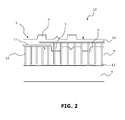
- Fig. 2 schematically represents a sectional view of a printed circuit board assembly 10 according to an embodiment disclosed herein.
- the printed circuit board assembly 10 comprises a printed circuit board (PCB) 2.
- the PCB 2 includes a non-conductive board consisting of a known material, for example, FR-4.
- the PCB 2 further includes at least one copper plane 11 and supports a plurality of electronic components 3, which are electrically connected to the copper plane 11.
- the one or more copper planes 11 are constituted by conductive pathways or tracks that electrically connect the electronic components and are etched from copper sheets laminated onto the non-conductive board. There may also be multiple copper trace layers within the thickness of the board.
- the PCB 2 supports on both sides electronic components, as well as tracks and soldering spots. However, it is also possible that only one side of the PCB 2 is populated.
- the PCB assembly 10 further comprises a thermally conducting chassis 4 extending substantially parallel to the PCB 2.
- the chassis 4 is used to fix the PCB 2 to the sea case (not shown).
- the thermal pad 5 may be of plastic or silicon-based material, for example, Kapton, which may additionally be paraffin-wax coated.
- the thermal pad 5 may have a thickness of several millimeters, for example, about 3 mm.
- the remaining air gaps 6 between the thermal pad 5 and the PCB 2 may be simply expressed as a mean residual air gap of a given width.
- the PCB 2 is clamped, screwed, or otherwise fixed to the chassis 4.
- the thermal pad 5 is moderately compressed so as to enable it to substantially fill the gap between the PCB 2 and the chassis 4.
- the pins 12 do not touch the chassis 4.
- a gap 13 is left between each of the pins 12 and the chassis, as shown in Fig. 2 .
- the pins 12 penetrate the thermal pad 5 over a given distance so as to enable the penetration of substantially all the pins 12 into the pad 5 at any time.
- the pins 12 may, for example, end up at about 0.5 mm from the chassis 4.
- the length of the pins 12 may substantially correspond to an average distance between the printed circuit board (2) and the chassis (4).
- the pins 12 may all have the same length, or different lengths.
- the pins 12 may be electrically conducting.
- a good electrical conductivity is normally correlated with a good thermal conductivity. The spacing between the pins 12 and the chassis 4 thus prevents electrical contact between each of the pins 12 and the chassis 4.
- the chassis 4, which acts as a heat sink, may be electrically conducting.
- the chassis 4 may be of aluminum.
- the chassis may be of the same electrical potential as one or more copper planes 11.
- One or several of the pins 12 connecting to this or these copper planes 11 may then be in electrically conducting contact with the chassis 4.
Landscapes
- Engineering & Computer Science (AREA)
- Microelectronics & Electronic Packaging (AREA)
- Manufacturing & Machinery (AREA)
- Cooling Or The Like Of Electrical Apparatus (AREA)
- Structure Of Printed Boards (AREA)
Abstract
The invention relates to a printed circuit board assembly (10) comprising a printed circuit board (2) including at least one copper plane (11) and supporting a plurality of electronic components (3) electrically connected to at least one copper plane (11), a thermally conducting chassis (4) extending substantially parallel to the printed circuit board (2), a thermal pad (5) substantially filling a gap between the printed circuit board (2) and the chassis (4) so as to enable heat transfer from the printed circuit board (2) to the chassis (4), and a plurality of thermally conducting pins (12) extending from the at least one copper plane (11) towards the chassis (4) so as to penetrate the thermal pad (5).
Description
- The present invention relates to the field of printed circuit board assemblies. More particularly, the invention concerns a printed circuit board assembly enabling improved heat transfer.
- Printed circuit boards (PCBs) support electronic components and include wiring and soldering tracks. In order to function correctly and to optimize the lifetime of the components, the heat generated by the components in operation has to be dissipated properly.
- Several techniques are employed to transfer heat from the PCB to its environment. For example, heat may be transferred by natural air cooling. However, the cooling effect may be insufficient for some applications. Forced air cooling, for example in the form of a fan blowing air onto the PCB, may be prohibited for reliability reasons, in particular in the case of PCBs being part of subsea equipment.
- Heat may also be transferred by conduction from the PCB to its support. This is usually the case for subsea equipment. The support is typically a chassis fixed to the sea case containing the PCB(s) and onto which the PCB(s) are clamped, screwed, or otherwise fixed. The heat conduction method must respond to several constraints. For example, electric isolation shall generally be maintained between the PCB and the support. Further, the PCB surface is normally scattered with electronic components, tracks, soldering areas, and the like, which can prevent a good thermal contact of the PCB with the support.
- A known printed
circuit board assembly 1 employing heat conduction cooling is represented inFig. 1 . A thick thermally conductive, orthermal pad 5 is fitted between aPCB 2 and itssupport 4, or chassis. The PCB 2 supports multiple heat dissipating,electronic components 3, wiring, soldering spots, etc., leading to surfaces of thePCB 2 having a roughness of several millimeters. Thethermal pad 5 is of a thermally conducting material and transfers the heat from thePCB 2 to itssupport 4, which acts as a heat sink. Thanks to its deformability increasing with temperature, thethermal pad 5 is normally used to fill air gaps between thePCB 2 and thesupport 4. - However, thermal pads are usually not compressible and deformable enough so as to come reliably in close contact with all parts of the PCB, in spite of possible PCB deformations, bumps, vibrations, or differential shrinkage. Thus,
air gaps 6, as illustrated inFig. 1 , may persist between thethermal pad 5 and thePCB 2. Further, the positioning of the thermal pads may vary in time, they may undergo debonding from the PCB, and the materials used for the thermal pads are subject to ageing, which greatly compromises their reliability. - Another heat transfer arrangement employs a metal core PCB technology, which consists in directly integrating an electrically insulated metallic piece into the PCB. The metallic core is linked to an external heat sink to conduct heat away from the PCB. Even though this technique shows good thermal performance, it implies, however, a very sophisticated and expensive PCB fabrication technology.
- According to the foregoing, there exists a need for a printed circuit board assembly providing for an efficient, durable, simple and cost-effective heat conduction cooling.
- Embodiments of the present invention provide a printed circuit board assembly enabling improved heat conduction cooling of the printed circuit board and the heat dissipative electronic components arranged on it, wherein the assembly resolves the above mentioned problems.
- According to a first aspect, there is provided a printed circuit board assembly printed circuit board assembly comprising:
- a printed circuit board including at least one copper plane and supporting a plurality of electronic components electrically connected to the at least one copper plane,
- a thermally conducting chassis extending substantially parallel to the printed circuit board,
- a thermal pad substantially filling a gap between the printed circuit board and the chassis so as to enable heat transfer from the printed circuit board to the chassis, and
- a plurality of thermally conducting pins extending from the at least one copper plane towards the chassis so as to penetrate the thermal pad.
- The printed circuit board assembly according to the present disclosure provides a continuous, reliable heat transfer path from the dissipative electronic components to the chassis. The heat is transferred from the electronic components to the at least one copper plane, along the copper plane, from the copper plane to the thermally conducting pins, along the pins and into the thermal pad, and finally from the thermal pad to the chassis. This heat conduction mechanism is reliable even in the absence of a direct or perfect contact of the printed circuit board with the thermal pad.
- Preferably, the pins are electrically conducting.
- In some embodiments, the chassis is electrically conducting having the same electrical potential as the at least one copper plane, and at least one of the pins connecting to the at least one copper plane is in electrically conducting contact with the chassis.
- Alternatively, the printed circuit board includes a plurality of copper planes all similar to and being at the same electrical potential as the at least one copper plane, and wherein at least one pin of each copper plane of the plurality of copper planes is in electrically conducting contact with the chassis.
- In some embodiments, a surface of the chassis next to the thermal pad is covered with an electrically insulating varnish and at least one of the pins is in physical contact with the varnished surface.
- Preferably, the pins are parallel to each other.
- In some embodiments, the pins extend substantially perpendicularly from the at least one copper plane.
- In some embodiments, the pins are extending from the at least one copper plane according to a chessboard grid. Advantageously, the pins are spaced between 2 mm and 3.5 mm with respect to each other, and preferably 2 mm, 2.54 mm, or 3.17 mm.
- Preferably, the diameter of each of the pins is about 1 mm.
- Advantageously, the pins are of copper or aluminum.
- In some embodiments, at least one of the plurality of pins is constituted by a lead of one of the plurality of electronic components.
- Advantageously, the length of the pins substantially corresponds to an average distance between the printed circuit board and the chassis.
- Additional aspects and advantages of printed circuit board assemblies according to embodiments disclosed herein will be set forth, in part, in the detailed description, figures and any claims which follow, and, in part, will be derived from the detailed description. It is to be understood that both the foregoing general description and the following detailed description are only exemplary and do not limit the claimed inventions.
- Exemplary embodiments of printed circuit board assemblies according to this disclosure are described with reference to the accompanying drawings, in which:
-
Fig. 1 , already described, schematically represents a sectional view of a known printed circuit board assembly; -
Fig. 2 schematically represents a sectional view of a printed circuit board assembly according to an embodiment disclosed herein; and -
Fig. 3 illustrates heat conduction in a printed circuit board assembly according to embodiments disclosed herein. - The figures and the following description illustrate exemplary embodiments. In the figures, elements with similar structures and/or functions may be denoted by like reference numerals.
-
Fig. 2 schematically represents a sectional view of a printedcircuit board assembly 10 according to an embodiment disclosed herein. The printedcircuit board assembly 10 comprises a printed circuit board (PCB) 2. ThePCB 2 includes a non-conductive board consisting of a known material, for example, FR-4. The PCB 2 further includes at least onecopper plane 11 and supports a plurality ofelectronic components 3, which are electrically connected to thecopper plane 11. The one ormore copper planes 11 are constituted by conductive pathways or tracks that electrically connect the electronic components and are etched from copper sheets laminated onto the non-conductive board. There may also be multiple copper trace layers within the thickness of the board. As shown in the embodiment ofFig. 2 , thePCB 2 supports on both sides electronic components, as well as tracks and soldering spots. However, it is also possible that only one side of thePCB 2 is populated. - The electrical circuit implemented by the
PCB 2 may comprise several equipotential areas (for example, ground, +15 V, -15 V) that are each electrically linked with adifferent copper plane 11, covering a large part of thePCB 2 surface. The example ofFig. 2 shows two copper planes 11. - The
PCB assembly 10 further comprises a thermally conductingchassis 4 extending substantially parallel to thePCB 2. In the case of thePCB 2 being implemented with subsea equipment, thechassis 4 is used to fix thePCB 2 to the sea case (not shown). Athermal pad 5, substantially filling a gap between thePCB 2 and thechassis 4, enables heat transfer from thePCB 2 to thechassis 4. Thethermal pad 5 may be of plastic or silicon-based material, for example, Kapton, which may additionally be paraffin-wax coated. Thethermal pad 5 may have a thickness of several millimeters, for example, about 3 mm. The remainingair gaps 6 between thethermal pad 5 and thePCB 2 may be simply expressed as a mean residual air gap of a given width. - The
PCB assembly 10 further comprises a plurality of thermally conducting pins 12. Thepins 12 extend from the at least onecopper plane 11 towards thechassis 4 so as to penetrate thethermal pad 5. Thepins 12 constitute a reliable thermally conductive contact between thePCB 2 and thethermal pad 5, even if thethermal pad 5 does not perfectly adapt the surface of thePCB 2. Thepins 12 may be attached to the at least onecopper plane 11 by soldering. - The
PCB 2 is clamped, screwed, or otherwise fixed to thechassis 4. Thereby, thethermal pad 5 is moderately compressed so as to enable it to substantially fill the gap between thePCB 2 and thechassis 4. According to an embodiment, thepins 12 do not touch thechassis 4. Thus, agap 13 is left between each of thepins 12 and the chassis, as shown inFig. 2 . Thepins 12 penetrate thethermal pad 5 over a given distance so as to enable the penetration of substantially all thepins 12 into thepad 5 at any time. The longer thepins 12 in relation to an average distance between thePCB 2 and thechassis 4, the better is the heat conduction performance of theassembly 10. Thepins 12 may, for example, end up at about 0.5 mm from thechassis 4. The length of thepins 12 may substantially correspond to an average distance between the printed circuit board (2) and the chassis (4). Thepins 12 may all have the same length, or different lengths. - In some embodiments, the
pins 12 may be of copper or of aluminum. Copper is an excellent thermal conductor, with a thermal conductivity of about 400 W/(m·K). Aluminum also has good thermal conductivity (of about 235 W/(m·K)) and is a relatively cheap metal. For comparison, the materials used for the thermal pad have thermal conductivities in the range of 1 to 5 W/(m·K), and air 0.03 W/(m·K). - As it will be appreciated by the skilled person, the
pins 12 may be electrically conducting. In the case the pins are of metal or metal alloy, a good electrical conductivity is normally correlated with a good thermal conductivity. The spacing between thepins 12 and thechassis 4 thus prevents electrical contact between each of thepins 12 and thechassis 4. - Furthermore, the
chassis 4, which acts as a heat sink, may be electrically conducting. For example, thechassis 4 may be of aluminum. In this case, the chassis may be of the same electrical potential as one or more copper planes 11. One or several of thepins 12 connecting to this or thesecopper planes 11 may then be in electrically conducting contact with thechassis 4. - In some embodiments, a surface of the
chassis 4 that is next to thethermal pad 5 may be covered with an electrically insulating varnish. At least one of thepins 12 may then be in physical contact with the varnished surface. - The physical contact of the
pins 12 with thechassis 4 may help to correctly position thePCB 2 with respect to thechassis 4 and to enhance the mechanical stability of thePCB assembly 10. - Advantageously, in some embodiments, the
pins 12 are parallel to each other. Preferably, thepins 12 extend substantially perpendicularly from the at least onecopper plane 11, as with the embodiment shown inFig. 2 . - In some embodiments, the
pins 12 may be arranged on the at least onecopper plane 11 according to a grid. Preferably, thepins 12 extend from the at least onecopper plane 11 according to a chessboard grid. Thepins 12 may be spaced between 2 mm and 3.5 mm with respect to each other. The diameter of each of thepins 12 may be about 1 mm. For example, thepins 12 may be spaced 2 mm, 2.54 mm (0.1 in), or 3.17 mm (0.125 in). These spacing values permit to route wirings to other layers in thePCB 2. Thepins 12 may, for example, about 2 to 3 mm long. - In some embodiments, at least one of the plurality of
pins 12 may be constituted by a lead of one of the plurality ofelectronic components 3. The pins or leads, typically of copper, of theelectronic components 3 are usually cut at the soldering slots of thePCB 2. One or more of them may be maintained longer so as to deeply penetrate thethermal pad 5, such as described hereinabove with respect to thepins 12. -
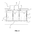
Fig. 3 illustrates the heat transfer occurring in thePCB assembly 10 according to embodiments disclosed herein, in the case thepins 12 do not touch thechassis 4. The heat transfer is schematically indicated by arrows 20-24. The heat is conducted from theelectronic components 3 to the at least one copper plane 11 (arrow 20), along the copper plane 11 (arrows 21), from thecopper plane 11 to thepins 12, along the pins 12 (arrows 22) and radially into the thermal pad 5 (arrows 23), and finally from thethermal pad 5 to the chassis 4 (arrows 24). In the case thepins 12 touch the chassis, the heat conduction figure is similar, with additional direct heat conduction from thepins 12 to thechassis 4. From thechassis 4, the heat may then be transferred, for example, to the sea case and into the water (not shown). - For a
typical PCB 2, heat transfer performances may be estimated to the following average values: - natural convection: 10 W/(m2·K),
- forced convection using an air fan: 100 W/(m2·K),
- known PCB assembly having a thermal pad of a thickness of about 3 mm with a mean residual air gap of about 0.2 mm between the thermal pad and the PCB: 100 W/(m2·K),
- PCB assembly according to embodiments disclosed herein (pins of about 1 mm in diameter, spaced 2.54 mm (0.1 in), and ending up at about 0.5 mm from the chassis): 1000 W/(m2·K).
- The heat conduction mechanism as described above is reliable and efficient even in the absence of a direct or perfect contact of the printed circuit board with the thermal pad. The printed circuit board assembly according to the present disclosure provides a continuous, reliable heat transfer path from the dissipative electronic components to the chassis.
- Although some embodiments of the present invention have been illustrated in the accompanying drawings and described in the foregoing detailed description, it should be understood that the present invention is not limited to the disclosed embodiments, but is capable of numerous rearrangements, modifications, and substitutions without departing from the invention as set forth and defined by the following claims.
Claims (14)
- A printed circuit board assembly (10) comprising:a printed circuit board (2) including at least one copper plane (11) and supporting a plurality of electronic components (3) electrically connected to the at least one copper plane (11),a thermally conducting chassis (4) extending substantially parallel to the printed circuit board (2),a thermal pad (5) substantially filling a gap between the printed circuit board (2) and the chassis (4) so as to enable heat transfer from the printed circuit board (2) to the chassis (4), anda plurality of thermally conducting pins (12) extending from the at least one copper plane (11) towards the chassis (4) so as to penetrate the thermal pad (5).
- The printed circuit board assembly (10) according to claim 1, wherein the pins (12) are electrically conducting.
- The printed circuit board assembly (10) according to claim 2, wherein the chassis (4) is electrically conducting having the same electrical potential as the at least one copper plane (11), and wherein at least one of the pins (12) connecting to the at least one copper plane (11) is in electrically conducting contact with the chassis (4).
- The printed circuit board assembly (10) according to claim 3, wherein the printed circuit board (2) includes a plurality of copper planes all similar to the at least one copper plane (11) and being at the same electrical potential as the at least one copper plane (11), and wherein at least one pin (12) of each copper plane of the plurality of copper planes is in electrically conducting contact with the chassis (4).
- The printed circuit board assembly (10) according to claim 1 or 2, wherein a surface of the chassis (4) next to the thermal pad (5) is covered with an electrically insulating varnish and at least one of the pins (12) is in physical contact with the varnished surface.
- The printed circuit board assembly (10) according to any of the preceding claims, wherein the pins (12) are parallel to each other.
- The printed circuit board assembly (10) according to any of the preceding claims, wherein the pins (12) extend substantially perpendicularly from the at least one copper plane (11).
- The printed circuit board assembly (10) according to any of the preceding claims, wherein the pins (12) are extending from the at least one copper plane (11) according to a chessboard grid.
- The printed circuit board assembly (10) according to claim 8, wherein the pins (12) are spaced between 2 mm and 3.5 mm with respect to each other.
- The printed circuit board assembly (10) according to claim 8 or 9, wherein the pins (12) are spaced 2 mm, 2.54 mm, or 3.17 mm with respect to each other.
- The printed circuit board assembly (10) according to any of the preceding claims, wherein the diameter of each of the pins (12) is about 1 mm.
- The printed circuit board assembly (10) according to any of claims 2 to 11, wherein the pins (12) are of copper or aluminum.
- The printed circuit board assembly (10) according to any of claims 2 to 11, wherein at least one of the plurality of pins (12) is constituted by a lead of one of the plurality of electronic components (3).
- The printed circuit board assembly (10) according to any of the preceding claims, wherein the length of the pins substantially corresponds to an average distance between the printed circuit board (2) and the chassis (4).
Priority Applications (1)
| Application Number | Priority Date | Filing Date | Title |
|---|---|---|---|
| EP13306059.0A EP2830399A1 (en) | 2013-07-23 | 2013-07-23 | Printed circuit board cooling |
Applications Claiming Priority (1)
| Application Number | Priority Date | Filing Date | Title |
|---|---|---|---|
| EP13306059.0A EP2830399A1 (en) | 2013-07-23 | 2013-07-23 | Printed circuit board cooling |
Publications (1)
| Publication Number | Publication Date |
|---|---|
| EP2830399A1 true EP2830399A1 (en) | 2015-01-28 |
Family
ID=48918332
Family Applications (1)
| Application Number | Title | Priority Date | Filing Date |
|---|---|---|---|
| EP13306059.0A Withdrawn EP2830399A1 (en) | 2013-07-23 | 2013-07-23 | Printed circuit board cooling |
Country Status (1)
| Country | Link |
|---|---|
| EP (1) | EP2830399A1 (en) |
Citations (3)
| Publication number | Priority date | Publication date | Assignee | Title |
|---|---|---|---|---|
| US5933324A (en) * | 1997-12-16 | 1999-08-03 | Intel Corporation | Apparatus for dissipating heat from a conductive layer in a circuit board |
| DE19909505A1 (en) * | 1999-03-04 | 2000-09-21 | Daimler Chrysler Ag | Process for the production of circuit arrangements |
| EP1659839A2 (en) * | 2004-11-19 | 2006-05-24 | Delphi Technologies, Inc. | Thermal management of surface-mount circuit devices on laminate ceramic substrate |
-
2013
- 2013-07-23 EP EP13306059.0A patent/EP2830399A1/en not_active Withdrawn
Patent Citations (3)
| Publication number | Priority date | Publication date | Assignee | Title |
|---|---|---|---|---|
| US5933324A (en) * | 1997-12-16 | 1999-08-03 | Intel Corporation | Apparatus for dissipating heat from a conductive layer in a circuit board |
| DE19909505A1 (en) * | 1999-03-04 | 2000-09-21 | Daimler Chrysler Ag | Process for the production of circuit arrangements |
| EP1659839A2 (en) * | 2004-11-19 | 2006-05-24 | Delphi Technologies, Inc. | Thermal management of surface-mount circuit devices on laminate ceramic substrate |
Similar Documents
| Publication | Publication Date | Title |
|---|---|---|
| EP2525632B1 (en) | Systems for circuit board heat transfer and method of assembling same | |
| US10504813B2 (en) | Heat sink assemblies for surface mounted devices | |
| JP2016504775A (en) | Circuit board assembly | |
| KR101908098B1 (en) | Printed circuit board, circuit, and method for the production of a circuit | |
| CN105848405A (en) | Circuit board with heat dissipation structure and making method thereof | |
| EP2975640A2 (en) | Electronic device assembly | |
| WO2012013546A1 (en) | An electronic heating module and a method for manufacturing the same | |
| CN101111144B (en) | Thermal conduit | |
| CN105337100B (en) | Arrangements of electric connection | |
| KR20170054842A (en) | Heat radiation member and printed circuit board having the same | |
| JP6569377B2 (en) | Cable connector and wiring board | |
| KR102053275B1 (en) | Junction block with heat dissipation structure | |
| CN116250379A (en) | Circuit Boards and Circuit Assemblies | |
| EP2830399A1 (en) | Printed circuit board cooling | |
| WO2017115627A1 (en) | Inverter | |
| TWI578862B (en) | Circuit module with lateral surface-mound pads and the corresponding system of the circuit module | |
| US9226384B2 (en) | Circuit board system comprising a cooling arrangement | |
| KR101602706B1 (en) | Embedded substrate having metal foil for radiating heat and method manufacturing method thereof | |
| KR20190076627A (en) | Lighting apparatus and manufacturing method of the same | |
| JP6500210B2 (en) | Metal plate resistor | |
| US9107296B2 (en) | Thermo/electrical conductor arrangement for multilayer printed circuit boards | |
| JP2019140321A (en) | Electronic component mounting substrate and electronic device | |
| KR101084342B1 (en) | Heat dissipation board | |
| US10201095B2 (en) | Method for manufacturing a circuit board system with mechanical protection | |
| US20150342026A1 (en) | Electric assembly to be mounted on a top-hat rail |
Legal Events
| Date | Code | Title | Description |
|---|---|---|---|
| 17P | Request for examination filed |
Effective date: 20130723 |
|
| AK | Designated contracting states |
Kind code of ref document: A1 Designated state(s): AL AT BE BG CH CY CZ DE DK EE ES FI FR GB GR HR HU IE IS IT LI LT LU LV MC MK MT NL NO PL PT RO RS SE SI SK SM TR |
|
| AX | Request for extension of the european patent |
Extension state: BA ME |
|
| PUAI | Public reference made under article 153(3) epc to a published international application that has entered the european phase |
Free format text: ORIGINAL CODE: 0009012 |
|
| STAA | Information on the status of an ep patent application or granted ep patent |
Free format text: STATUS: THE APPLICATION IS DEEMED TO BE WITHDRAWN |
|
| 18D | Application deemed to be withdrawn |
Effective date: 20150729 |