EP2830239B1 - Procédé, système et dispositif émetteur-récepteur pour signaux optiques numériques à transmission bidirectionnelle via une liaison de transmission optique - Google Patents
Procédé, système et dispositif émetteur-récepteur pour signaux optiques numériques à transmission bidirectionnelle via une liaison de transmission optique Download PDFInfo
- Publication number
- EP2830239B1 EP2830239B1 EP13003679.1A EP13003679A EP2830239B1 EP 2830239 B1 EP2830239 B1 EP 2830239B1 EP 13003679 A EP13003679 A EP 13003679A EP 2830239 B1 EP2830239 B1 EP 2830239B1
- Authority
- EP
- European Patent Office
- Prior art keywords
- optical
- signal
- bit
- digital signal
- txi
- Prior art date
- Legal status (The legal status is an assumption and is not a legal conclusion. Google has not performed a legal analysis and makes no representation as to the accuracy of the status listed.)
- Not-in-force
Links
Images


Classifications
-
- H—ELECTRICITY
- H04—ELECTRIC COMMUNICATION TECHNIQUE
- H04B—TRANSMISSION
- H04B10/00—Transmission systems employing electromagnetic waves other than radio-waves, e.g. infrared, visible or ultraviolet light, or employing corpuscular radiation, e.g. quantum communication
- H04B10/25—Arrangements specific to fibre transmission
- H04B10/2575—Radio-over-fibre, e.g. radio frequency signal modulated onto an optical carrier
-
- H—ELECTRICITY
- H04—ELECTRIC COMMUNICATION TECHNIQUE
- H04B—TRANSMISSION
- H04B10/00—Transmission systems employing electromagnetic waves other than radio-waves, e.g. infrared, visible or ultraviolet light, or employing corpuscular radiation, e.g. quantum communication
- H04B10/25—Arrangements specific to fibre transmission
- H04B10/2589—Bidirectional transmission
-
- H—ELECTRICITY
- H04—ELECTRIC COMMUNICATION TECHNIQUE
- H04B—TRANSMISSION
- H04B10/00—Transmission systems employing electromagnetic waves other than radio-waves, e.g. infrared, visible or ultraviolet light, or employing corpuscular radiation, e.g. quantum communication
- H04B10/50—Transmitters
- H04B10/516—Details of coding or modulation
- H04B10/5167—Duo-binary; Alternative mark inversion; Phase shaped binary transmission
-
- H—ELECTRICITY
- H04—ELECTRIC COMMUNICATION TECHNIQUE
- H04J—MULTIPLEX COMMUNICATION
- H04J14/00—Optical multiplex systems
- H04J14/02—Wavelength-division multiplex systems
-
- H—ELECTRICITY
- H04—ELECTRIC COMMUNICATION TECHNIQUE
- H04J—MULTIPLEX COMMUNICATION
- H04J14/00—Optical multiplex systems
- H04J14/02—Wavelength-division multiplex systems
- H04J14/0227—Operation, administration, maintenance or provisioning [OAMP] of WDM networks, e.g. media access, routing or wavelength allocation
- H04J14/0241—Wavelength allocation for communications one-to-one, e.g. unicasting wavelengths
- H04J14/0242—Wavelength allocation for communications one-to-one, e.g. unicasting wavelengths in WDM-PON
- H04J14/0249—Wavelength allocation for communications one-to-one, e.g. unicasting wavelengths in WDM-PON for upstream transmission, e.g. ONU-to-OLT or ONU-to-ONU
- H04J14/025—Wavelength allocation for communications one-to-one, e.g. unicasting wavelengths in WDM-PON for upstream transmission, e.g. ONU-to-OLT or ONU-to-ONU using one wavelength per ONU, e.g. for transmissions from-ONU-to-OLT or from-ONU-to-ONU
-
- H—ELECTRICITY
- H04—ELECTRIC COMMUNICATION TECHNIQUE
- H04J—MULTIPLEX COMMUNICATION
- H04J14/00—Optical multiplex systems
- H04J14/02—Wavelength-division multiplex systems
- H04J14/0278—WDM optical network architectures
- H04J14/0282—WDM tree architectures
-
- H—ELECTRICITY
- H04—ELECTRIC COMMUNICATION TECHNIQUE
- H04J—MULTIPLEX COMMUNICATION
- H04J14/00—Optical multiplex systems
- H04J14/02—Wavelength-division multiplex systems
- H04J14/0227—Operation, administration, maintenance or provisioning [OAMP] of WDM networks, e.g. media access, routing or wavelength allocation
- H04J14/0241—Wavelength allocation for communications one-to-one, e.g. unicasting wavelengths
- H04J14/0242—Wavelength allocation for communications one-to-one, e.g. unicasting wavelengths in WDM-PON
- H04J2014/0253—Allocation of downstream wavelengths for upstream transmission
Definitions
- the invention relates to a system and a method for bi-directionally transmitting digital optical signals over an optical transmission link as well as to an optical transceiver device for a respective system.
- WDM optical wavelength division multiplex
- ONU optical network units
- OLT optical line terminal
- RN remote node
- Each ONU connects at least one end-user to the RN.
- a single fiber is used for connecting the RN to the ONUs in order to save fiber usage.
- PON configurations with dual-fiber connection between the OLT and the RN are also widely used.
- a protection mechanism especially a fiber-protection method and hardware, may be implemented for the transmission link between the OLT and the RN.
- PONs enable a bi-directional point-to-point connection between each ONU and the OLT using dedicated optical channels, i.e. for each point-to-point connection a pair of downstream and upstream signals having predetermined optical wavelengths is used.
- the downstream channel signal transmitted from the OLT to the respective ONU and the upstream channel signal transmitted in the reverse direction may have identical or differing optical wavelengths.
- the plurality of downstream and upstream optical channel signals is transmitted as a combined WDM signal within the transmission link between the OLT and the RN.
- Typical low-cost solutions for colorless ONUs are based on the use of reflective optical transmitters like semiconductor optical amplifiers (RSOA), injection-locked Fabry-Perot laser diodes (IL-FP-LD) or reflective electro-absorption modulators with integrated semiconductor optical amplifiers (REAM-SOA) as optical transmitter components.
- RSOA semiconductor optical amplifiers
- IL-FP-LD injection-locked Fabry-Perot laser diodes
- RRM-SOA reflective electro-absorption modulators with integrated semiconductor optical amplifiers
- wavelength-reuse transmission systems In a PON design using such reflective optical transmitters, the downstream (channel) signals are reused in the ONUs in order to create an upstream signal having the same wavelength.
- wavelength-reuse transmission systems such a system for bi-directionally transmitting digital optical signals over an optical transmission link.
- the (optical) downstream (channel) signals must not use standard non-return-to-zero (NRZ) on-off keying (OOK) because for levels "0" sent, upstream modulation is impossible or subject to severe penalties.
- NRZ non-return-to-zero
- OLK on-off keying
- a level "0" or a logical value "0" of an amplitude-modulated optical signal shall be understood in such a way that an optical power of essentially zero is transported within the respective symbol interval. Therefore, another modulation format than NRZ-OOK must be chosen for the downstream signals. However, other modulation formats always involve additional effort and costs.
- a known approach for a WDM-PON applying wavelength-reuse is based on using frequency-shift keying (FSK) for the downstream signal, wherein this signal reveals an essentially constant envelope, and a standard OOK modulation format for the upstream signal.
- FSK frequency-shift keying
- any other modulation format may be used that produces a downstream signal having an essentially constant envelope, like any phase shift keying (FSK) format.
- IRZ inverse-return-to-zero
- the remodulating transmitter does not need to operate in saturation (for a comparison of these two alternatives see L. Giorgi et al: "WDM-PON based on Self-Seeded OLT and Wavelength Reuse at ONU", OFC/NFOEC 2013, IEEE, 17 March 2013, pages 1.3, XP032427363, ISBN: 978-1-4799-0457-0 ; for the former alternative see also WO 2010/025767 A1 ).
- a first optical transmit signal at a predetermined optical wavelength is created and supplied to a first end of an optical transmission link and transmitted in a first transmission direction to a second end of the optical transmission link.
- This first optical transmit signal is created in such a way that it can be reused at the second end of the transmission link for creating a second optical transmit signal, preferably by using a reflective modulator device.
- This second optical transmit signal is transmitted in a second transmission direction to the first end of the optical transmission link.
- Said first optical transmit signal is created according to a first binary digital signal in such a way that the bit information of the first binary digital signal is included in first sections of the symbol interval of the first optical transmit signal.
- Said second optical transmit signal is created by creating an optical wavelength reuse signal using the first optical transmit signal received at the second end of the optical transmission link.
- the optical wavelength reuse signal is modulated according to a second digital signal in such a way that the bit information of the second digital signal is included in second sections of the symbol interval of the first optical transmit signal received.
- a non-return-to-zero (NRZ) signal is used as first binary digital signal and the first optical transmit signal is an optical bit-interleaved seeding signal having a symbol rate equal to the bit rate of the NRZ signal, wherein the symbol interval of the optical bit-interleaved seeding signal is divided into two equally long sub-intervals or sections, the bit information of the first binary digital signal being transported in a first of the two sections and the second section being set to seeding level with respect to the optical power.
- the seeding level may of course be equal to the maximum (optical) power level of the digital optical bit-interleaved seeding signal.
- the optical bit-interleaved seeding signal is a duobinary coded optical bit-interleaved seeding signal.
- a duobinary coding leads to a reduction of the bandwidth of the first optical transmit signal that would otherwise be caused by dividing the symbol interval of the first optical transmit signal (and as a result also the second optical transmit signal) into two subintervals and merely using one of the subintervals for the data transmission in each direction.
- a decisive reduction of costs for implementing the transmission method is achieved.
- the invention is especially applicable for WDM-PON access networks providing bit-rates of 10 Gbit/s for each channel signal in the downstream and upstream direction.
- duobinary coding leads to the effect that the duobinary optical bit-interleaved seeding signal has a bandwidth less than the bandwidth of the first binary digital signal, i.e. in case of a 10 Gbit/s first binary digital signal the bandwidth is less than 10 GHz. This is a clear advantage over the known method of using an IRZ optical channel signal in the downstream direction and an OOK RZ scheme in the upstream direction.
- the invention requires a Mach-Zehnder modulator (MZM) or a dual electro-absorption modulator (dual EAM) in the OLT for creating the individual channel signals, but reduces the optical (components) bandwidth and enhances the tolerance against chromatic dispersion.
- MZM Mach-Zehnder modulator
- dual EAM dual electro-absorption modulator
- the duobinary optical bit-interleaved seeding signal is created by converting the first binary digital signal into a binary bit-interleaved digital signal having twice the bit rate of the first binary digital signal by dividing each bit interval into two equally long sub-intervals or sections, setting one section to the signal value of the first binary digital signal and setting the respective other section to the logical 1 value of the first binary digital signal, pre-coding the first binary digital signal and duobinary encoding the pre-coded binary bit-interleaved digital signal and modulating an optical light source having the predetermined optical wavelength using the pre-coded and encoded binary bit-interleaved digital signal as modulation signal.
- the duobinary optical bit-interleaved seeding signal is created by pre-coding the first binary digital signal and duobinary encoding the pre-coded first binary digital signal, low-pass filtering the pre-coded and encoded first binary digital signal in such a way that the filtered pre-coded and encoded first binary digital signal assumes in each transition between its extreme values a value which essentially equals the average value of the extreme values at times which essentially are equal to a quarter of the bit interval, and modulating an optical light source having the predetermined optical wavelength using the low-pass filtered pre-coded and encoded first binary digital signal as modulation signal.
- the duobinary optical bit-interleaved seeding signal may be created in such a way that it is a ternary optical signal with respect to the electric field and a binary digital signal with respect to the optical power. This can be achieved by using an optical modulator device, e.g.
- a Mach-Zehnder-Modulator or a dual electro-absorption-modulator which converts the duobinary modulating signal into the duobinary optical bit-interleaved seeding signal in such a way that the extreme values of the ternary modulation signal correspond to +E and -E and the intermediate value of the ternary modulation signal corresponds to 0, wherein +E, 0 and -E designates the amplitude of the electric vector of the optical bit-interleaved seeding signal.
- ISI intersymbol interference
- the optical bit-interleaved seeding signal received at the second end of the transmission link is divided, with respect to the optical power of the signal, into an optical receive signal and an optical branch-off signal, and the optical receive signal is used for receiving the first binary digital signal by detecting the optical power during the first of the two equally long sub-intervals or sections, e.g. by using an integrate-and-dump receiver.
- direct detection can be used which reduces the costs of the ONU components as compared to other modulation formats used for the first or downstream optical transmit signal.
- the optical branch-off signal can be used to create the optical wavelength reuse signal using a reflective modulator device, e.g. a reflective semiconductor optical amplifier, an injection-locked Fabry-Perot laser diode or a reflective electro-absorption modulator with an integrated semiconductor optical amplifier.
- a reflective modulator device e.g. a reflective semiconductor optical amplifier, an injection-locked Fabry-Perot laser diode or a reflective electro-absorption modulator with an integrated semiconductor optical amplifier.
- an NRZ or RZ coded signal can be used as second digital signal for creating the second optical transmit signal using the optical bit-interleaved seeding signal so that no complex and/or expensive pulse shaping is required in an ONU which is adapted to implement the method according to the invention.
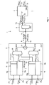
- Fig. 1 shows a schematic diagram of a WDM-PON 1 comprising an OLT 3, a remote node 5 and a plurality of ONUs 7. For simplicity, only a single ONU 7 is displayed.
- the WDM-PON uses a number n of optical channels, each optical channel using a dedicated optical channel bandwidth.
- a WDM port 9 of the OLT 3 is connected to a WDM port 11 of the RN 5 via a single optical fiber 13.
- Each of the ONUs 7 is connected to a channel port 14 i (1 ⁇ i ⁇ n) of the RN at a remote port 15 by a single optical fiber 17.
- the OLT comprises a number n of transceiver devices 19, each of which receives a first digital transmit signal S1 TXi (1 ⁇ i ⁇ n), which is supplied to a respective local input port 21 i (1 ⁇ i ⁇ n) of the OLT 3.
- the first digital transmit signal S1 TXi may e.g. be a 10 Gbit/s NRZ signal.
- Each transceiver device 19 further creates a first digital receive signal S1 RXi (1 ⁇ i ⁇ n) and supplies this signal to a local output port 23 i (1 ⁇ i ⁇ n).
- first digital transmit signals S1 TXi and the first digital receive signal S1 RXi may be optical signals or electrical signals.
- the transceiver devices 19 may convert optical signals S1 TXi into respective electrical signals, as generally electrical signals S1 TX are required to perform the signal processing within the transceiver devices 19.
- signals S1 RXi which are generally created as electrical signals, may be converted into respective optical signals, if required.
- Each transceiver device 19 creates a first optical transmit signal or first optical channel transmit signal S1 TX,Chi (1 ⁇ i ⁇ n) which transports the information included in the respective first digital signals S1 TXi and supplies the signal S1 TX,Chi , via an output port of the transceiver device 19, to a dedicated channel port of an optical multiplexer device 25, which may be realized as arrayed waveguide grating (AWG).
- a combined first optical WDM transmit signal S1 TX,WDM is output at a WDM port of the optical multiplexer device 25 and supplied to an optical circulator 27, which directs the first optical WDM transmit signal S1 TX,WDM to the WDM port 9 of the OLT 3.
- the WDM transmit signal S1 TX,WDM is transmitted via the optical fiber 13 to the WDM port 11 of the RN 5, which demultiplexes the WDM transmit signal S1 TX,WDM and outputs the optical channel transmit signals S1 TX,Chi to the respective ONU at the respective channel port 14.
- Each ONU 7 which may be regarded as transceiver device, receives the dedicated optical channel transmit signal S1 TX,Chi at its remote port 15 and creates a second digital receive signal S2 RXi (1 ⁇ i ⁇ n), which is output at a local output port 31 i (1 ⁇ i ⁇ n).
- the second digital receive signal S2 RXi is, of course, identical with the first digital transmit signal S1 TXi .
- each ONU 7 receives a second digital transmit signal S2 TXi (1 ⁇ i ⁇ n) at a local input port 33 and uses this signal to create a second optical transmit signal or second optical channel transmit signal S2 TX,Chi (1 ⁇ i ⁇ n) that is output at the remote port 15 of the ONU.
- the n second optical channel transmit signals S2 TX,Chi (1 ⁇ i ⁇ n) are multiplexed by the RN 5 into a second optical WDM transmit signal S2 TX,WDM and transmitted, via the WDM port 11 of the RN 5, to the WDM port 9 of the OLT 3.
- the circulator 27 directs the second optical WDM transmit signal S2 TX,WDM to a WDM port of a demultiplexer device 35, which may be realized as an AWG.
- the demultiplexer device 35 demultiplexes the second optical WDM transmit signal S2 TX,WDM into the individual second optical channel transmit signals S2 TX,Chi and outputs these signals at dedicated channel ports, which are connected to respective input ports of the dedicated transceiver devices 19.
- Each transceiver device 19 extracts the information included within the respective second optical channel transmit signal S2 TX,Chi and creates a corresponding first digital receive signal S1 RXi .
- the first digital receive signal S1 RXi is identical to the second digital transmit signal S2 TXi .
- the second digital transmit signals S2 Txi and the second digital receive signal S2 RXi may be optical signals or electrical signals.
- the ONUs 7 may convert optical signals S2 Txi into respective electrical signals, as generally electrical signals are required in order to perform the signal processing within the ONUs.
- Signals S2 RXi which are created as electrical signals, may be converted by the ONUs into respective optical signals, if required.
- the RN 5 shown in Fig. 1 which merely comprises a demultiplexing device, is, of course, to be understood as an example, only. Any configuration may be used that performs the demultiplexing of the WDM transmit signal S1 TX,WDM and the distribution of the individual optical channel transmit signals S1 TX,Chi to the dedicated ONUs 7.
- Each connection between the output port and the input port of a transceiver device 19 and the remote port 15 of an ONU 7 represents an optical transmission link for bi-directionally transmitting the respective first and second optical channel transmit signals S1 TX,Chi and S2 TX,Chi in the corresponding first and second transmission directions. That is, the transmission method according to the invention is not restricted to WDM-PONs but may also be applied for arbitrary optical point-to-point connections.
- the RN 5 and the ONUs 7, also dual-fiber connections may be used without any impact on the nature of the optical signals used for the bi-directional data transmission.
- the RN 5 may comprise two separate demultiplexer/multiplexer devices which are used for the upstream and downstream transmission direction, respectively.
- the downstream and upstream channel transmit signals S1 TX,Chi and S2 TX,Chi use the same optical channels also in case of a dual-fiber connection between the OLT 3 and the RN 5, a single demultiplexer/multiplexer device may be used in connection with suitable means, e.g. an optical circulator, adapted to combine and separate the transmission paths.
- each ONU 7 may be connected via a first fiber to a dedicated channel port of a first one of two separate demultiplexer/multiplexer devices in the RN5 and via a second fiber to a dedicated channel port of the second demultiplexer/multiplexer device in the RN5.
- a single demultiplexer/multiplexer device is provided in the RN5, only, the necessary separating and combining of the downstream and upstream transmission paths may be achieved by suitable means like optical separators, wherein the channel port of the single demultiplexer/multiplexer device is coupled to a first common port of the path separation/combination means and each of the two connecting fibers guiding the downstream and upstream channel transmit signals S1 TX,Chi and S2 TX,Chi are connected to a downstream and an upstream port of the dedicated port of the path separation/combination means.
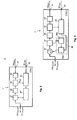
- Fig. 2 shows a schematic diagram of a first embodiment of an ONU 7 that is configured to realize the method according to the invention described below.
- the ONU 5 comprises a directional coupler 37 adapted to split the optical channel transmit signals S1 TX,Chi that is received at the remote port 15 with respect to its optical power.
- a first portion of the optical power represents an optical receive signal which is supplied to an opto-electrical converter device 39, e.g. a photodiode.
- the electrical signal output by the opto-electrical conversion device 39 is supplied to a clock and data recovery (CDR) device 41 which extracts the information transported in the signal received and creates a corresponding electrical digital signal which is supplied to a low-pass filter 43 for pulse shaping purposes.
- the filtered electrical signal represents the second digital receive signal S2 RX,Chi .
- the CDR device 41 is adapted to recover the clock information of the digital signal received.
- the clock information is used to synchronize the sampling or receiving mechanism with the signal received in order to correctly detect the bit information within each symbol interval.
- the optical channel transmit signals S1 TX,Chi received at each ONU is a binary digital signal, at least with respect to the optical power of the signal.
- the CDR device 41 may comprise a simple integrate-and-dump receiver. However, the CDR device 41 restricts the detection process to a selected section of the symbol interval, namely, to the first or second half of the symbol interval, as described below.
- the CDR device 41 supplies the recovered clock signal S CK also to a driver circuit 45 which receives the second digital transmit signal S2 TXi that is supplied to the local input port 33 of the ONU 7.
- the second digital transmit signal S2 TXi may be a 10 Gbit/s binary signal including the information to be transmitted to the OLT 3 in the upstream direction.
- the driver circuit 45 creates a second modulating signal S2 MODi supplied to a reflective modulator device 47 such as a reflective semiconductor optical amplifier (RSOA), an injection-locked Fabry-Perot laser diode (IL-FP LD) or a reflective electro-absorption modulator with an integrated semiconductor optical amplifier (REAM-SOA).
- a reflective modulator device 47 such as a reflective semiconductor optical amplifier (RSOA), an injection-locked Fabry-Perot laser diode (IL-FP LD) or a reflective electro-absorption modulator with an integrated semiconductor optical amplifier (REAM-SOA).
- the reflective modulator device 47 is able to reflect or reflect and amplify the second signal portion of the first optical channel transmit signal S1 TX,CHi which is split-off by the directional optical coupler 37 and supplied to an input/output port of the reflective modulator device 47.
- This branch-off signal serves for creating the second optical channel transmit signal S2 TX,CHi which is modulated according to the modulating signal S2 MODi and which has the same optical wavelength as the branch-off signal and thus as the first optical channel transmit signal S1 TX,CHi .
- a non-reflective modulator device 49 is used for creating the second optical channel transmit signal S2 TX,CHi .
- the non-reflective modulator device 49 may consist of an optical amplifier device 49a and an optical modulator device 49b, wherein these components are preferably integrated in a single unit or component.
- the optical branch-off signal is supplied to the optical amplifier device 49a which optically amplifies the branch-off signal created by the optical directional coupler and supplies the amplified signal to an optical modulator device 49b which modulates the amplified signal according to the modulating signal S MODi supplied by the driver circuit 45.
- an optical circulator 51 is necessary for separating/combining the receive path comprising the components for creating the second optical channel receive signal S1 TX,Chi in the respective ONU 7 and the transmit path comprising the components for creating the second optical channel transmit signal S2 TX,CHi .
- the optical circulator 51 receives the first optical channel transmit signal S1 TX,Chi and supplies it to the directional coupler 37. Further, the optical circulator 51 receives the second optical channel receive signal S2 TX,Chi output by the non-reflective modulator device 49.
- the signal processing which is necessary within the transceiver devices 19 of the OLT 3 and within the ONUs 7 in order to realize the data transmission method according to the invention will now be described in detail with reference to Figures 4 to 6 .
- the communication and data processing necessary for a point-to-point connection between a selected transceiver device 19 within the OLT 3 and a dedicated ONU 7 is considered which uses a dedicated optical channel of the WDM-PON.
- the selected transceiver device 19 receives the first digital transmit signal S TXi , which may be a 10 Gbit binary NRZ signal represented by the curve according to Fig. 4a .
- the bit interval of the NRZ signal S1 TXi is divided into a first and a second section of equal length.
- the transceiver device 19 may be configured to convert this signal into a respective (internal) NRZ signal.
- the transceiver device creates a bit-interleaved signal having twice the bit rate of the signal S1 TXi , wherein each first section of each bit interval is set to the value of the respective bit of the signal S1 TXi and wherein each second section of each bit interval is set to logical 1 (or "high").
- This (internal) signal is shown in Fig. 4b .
- This signal is duobinary pre-coded, i.e. the bit value of the duobinary precoded signal in Fig. 4c is obtained by inverting the bit-interleaved signal in Fig. 4b and applying an exlusive or (EXOR) operation on the inverted signal and the resulting signal (i.e. the signal which results from the EXOR operation) which is delayed by one bit interval.
- the resulting pre-coded signal which is shown in Fig. 4c , reveals a logical 0 bit as start value for the EXOR operation.
- S TX,Chi the phase of the E-vector of the electrical field is shifted by 180 degrees, which has no influence on the optical power of the signal that is detected in the ONU using a direct detection method.
- the transceiver device 19 duobinary encodes the pre-coded signal according to Fig. 4c which results in the signal as shown in Fig. 4d .
- the duobinary encoding which includes an adding operation of the bit value of the actual bit interval and the bit value of the previous bit interval, leads to the ternary signal shown in Fig. 4d .
- the signal processing including the pre-coding and encoding operations is performed in a signal processing device 52 comprised by a transmitter section of each transceiver device 19.
- the signal processing device 52 performs all operations necessary to create a first modulating signal S1 MODi using the respective first transmit signal S1 TXi .
- the modulating signal S1 MODi is supplied to an optical modulator device 53 of the transceiver device 19 or the transmitter section 19a of the transceiver device, respectively.
- the signal processing device 52 may be combined with a further signal processing device that is adapted to perform the necessary signal operations for the receiving of the second or upstream channel transmit signals S2 TX,Chi by a receiver section 19b of the transceiver device 19.
- a symmetrical modulating signal (“symmetrical” here means symmetrical with respect to the extreme values of the signal) is created by subtracting a value of one from the asymmetrical ternary signal.
- This symmetrical ternary modulating signal is shown in Fig. 4e .
- a low-pass filtering step may be applied in order to cancel high frequency noise from the signal, resulting in a filtered symmetrical duobinary pre-coded and encoded modulating signal S1 MODi (see Fig. 4f ) that is used in the transceiver device 19 to create the respective first optical channel transmit signal S1 TX,Chi .
- the modulating signal S1 MODi may be supplied to a suitable optical modulator device 53, e.g. a Mach-Zehnder modulator (MZM) or a dual electro-absorption modulator (dual EAM), which is driven between two transmission maxima including a 180-degree phase change.
- a suitable optical modulator device 53 e.g. a Mach-Zehnder modulator (MZM) or a dual electro-absorption modulator (dual EAM), which is driven between two transmission maxima including a 180-degree phase change.
- MZM Mach-Zehnder modulator
- dual EAM dual electro-absorption modulator
- the first optical channel transmit signal S1 TX,Chi will have the same shape with respect to the envelope of the electrical field vector E as the modulating signal S1 MODi according to Fig. 4f .
- the optical power of the first optical channel transmit signal S1 TX,Chi reveals a shape of the envelope corresponding to the squared envelope of the E-vector of the signal S1 TX,Chi , which is essentially 0 for bit values 0 of the NRZ signal S1 TXi and which is unequal to 0 in bit intervals that correspond to bit values 1 in the NRZ signal.
- the method thus produces a first optical channel transmit signal S1 TX,Chi which includes the bit information of the first transmit signal S1 TXi in a first half section of the symbol interval of the first optical channel transmit signal S1 TX,Chi and which includes an optical seeding power in the second half section of each symbol interval.
- the receiving and modulating function carried out in the ONU 7 may be adopted in a suitable manner by adjusting the synchronization of the receiving and modulating processes.
- bit-interleaved signal shown in Fig. 4b was directly used for creating a corresponding optical signal, the required bandwidth would increase by essentially the factor two. Additionally, the advantage of a duobinary pre-coded and encoded signal with respect to the reduced intersymbol interference and increased dispersion tolerance would be given up.
- the transceiver device in an ONU can recover the information included in the first optical channel transmit signal S1 TX,Chi by direct detection (i.e. evaluating the optical power of the signal received) applied to the first half section of each symbol interval.
- symbol interval is used with respect to the first and second optical channel transmit signal S1 TX,Chi and S2 TX,Chi as these signals are - at least with respect to the optical field vectors - ternary signals.
- the symbol interval is defined in such a way that each symbol interval includes the information of a single bit (or bit interval) of the respective NRZ signal S1 TXi .
- the CDR device 41 of an ONU recovers the clock of the NRZ signal S1 TXi and thus the signal S1 TX,Chi .
- the CDR device 41 which includes a receiver device, uses this recovered clock to control the receiver device in such a way that only the respective (first) half section of each symbol interval is used for the signal detection.
- Fig. 5e shows this method by a curve indicating the time intervals or first half sections I 1 of the bit intervals T B in which the bit information of the NRZ signal is included.
- Fig. 5f illustrates the second half sections I 2 of each symbol interval T B which include the seeding power or seeding "half-bits". These sections of the symbol intervals of the first optical channel transmit signal S1 TX,Chi received at an ONU can be used to create the second optical channel transmit signal S2 TX,Chi as described above.
- the driver circuit 45 may use this signal to effect a modulation of the optically amplified branch-off signal within the second sections I 2 of the symbol interval T B , only. This is shown in Fig.
- FIG. 5g illustrating the optical power of a second optical channel transmit signal S2 TX,Chi which has been created using a first optical channel transmit signal S1 TX,Chi that has been received at the ONU.
- the second optical channel transmit signal S2 TX,Chi is created in such a way that the information included in the first half section of the symbol interval of the signal S1 TX,Chi is deleted (the optical power in the second sections is set to zero) in order to reduce interference.
- This can be effected by using an RZ coding for the modulating signal S2 MODi .
- the respective transceiver device is also adapted to recover the clock from the signal received and to synchronize the receiver to the second half sections of the signal received for recovering the information included in these second sections of each symbol interval T B .
- Fig. 6 illustrates signal sequences in connection with a simplified method to create a duobinary pre-coded and encoded first optical channel transmit signal S1 TX,Chi in the OLT 3.
- duobinary encoding can be effected by just low-pass filtering the pre-coded signal. This is apparent from a comparison of Figs. 4c and 4f .
- a low-pass filtering applied to the pre-coded signal in Fig. 4c leads to a similar signal revealing a given slope at the rising and trailing edges.
- the low-pass filter can be designed such that the filtered (symmetrical) signal crosses the time axis in essentially the same points as the filtered (symmetrical) signal in Fig. 4f .
- a low-pass filter having a filter bandwidth of approximately 0.35 times the bit rate of the respective signal is used.
- a transceiver device 19 adapted to realize the data transmission method or creating of a first optical channel transmit signal S1 TX,Chi as illustrated with the signals in Fig. 6 , respectively, the following steps are performed: in a first step, the first transmit signal S1 TXi ( Fig. 6a ), which is the respective NRZ signal, is duobinary pre-coded as described above.
- the signal sequence in Fig. 6a is identical to the signal sequence in Fig. 4a
- the pre-coded signal shown in Fig. 6b (the signal sequence has already been made symmetrical with respect to the extreme values) is inverse as compared to the corresponding signal in Fig. 4c . This is due to the fact that in Fig.
- a value of logical 1 has been used as start value for the pre-coding process.
- this signal as modulating signal S1 MODi that is supplied to an optical modulator device like a MZM or a dual EAM
- a ternary optical signal with respect to the electrical field vector envelope is created, which is a binary optical signal with respect to the optical power envelope.
- an inversion of the modulator signal leads to the identical optical signal as far as the optical power envelope is concerned.
- the decisive difference between the well-known duobinary encoding using a low-pass filter and the present method of creating a bit-interleaved modulating signal S1 MODi is that the low-pass filter must be designed in such a way that the zero-crossings of the filtered duobinary (ternary) modulating signal S1 MODi are essentially in the center of the first half-section of the symbol interval (which is equal to the bit interval of the NRZ signal S1 TXi ), i.e.
- the slope of the filtered duobinary modulating signal S1 MODi is chosen such that the signal zero-crossings are essentially at a quarter of the bit or symbol interval (or at three quarters of the bit or symbol interval, if the second half section of the symbol interval is used for transmitting the information of the first transmit signal S1 TXi and the seeding "half-bit" is included within the first half section).
- the low-pass filtering is effected using a low-pass filter that reveals a (3dB) filter bandwidth of approximately 0.7 times the bit-rate of the NRZ first transmit signal S1 TXi .
- defining merely the filter bandwidth is not sufficient to characterize a suitable low-pass filter without defining the type and/or order of the filter.
- the low-pass filtering of the pre-coded signal in Fig. 6b as described above is equivalent to the insertion of seeding "half-bits".
- the advantage of the filtered coding method as compared to the direct insertion of interleave bits according to the coding method illustrated with the signals in Fig. 4 and 5 is that the coder device included in the signal processing device 52 of the transmitter section 19a of the transceiver device 19 must run at the bit-rate of the NRZ signal, only, whereas in the direct insertion method as described above with reference to Figs. 4 and 5 the coder device must run at twice the bit-rate of the NRZ signal S1 TXi .
- the optical modulator devices 53 run in both cases at around the bandwidth of the NRZ signal due to the bandwidth reduction achieved by the duobinary coding.
- the invention provides a data transmission method applying wavelength reuse of a downstream signal using an NRZ bit-interleaved signal in the downstream direction and any arbitrary amplitude modulation format to transmit the information included in an upstream digital signal in the upstream direction, wherein the signal portion according to the interleave bits included in the downstream signal, which is received and reused (amplified and modulated) at the second end of the transmission link to create a corresponding upstream signal, is used transport the information in the upstream direction.
- NRZ or RZ pulse shaping may be applied to modulate the interleave bit portions of the wavelength reuse signal created at the second end of the transmission link.
- the method can be implemented with or without optical duobinary coding of the optical downstream transmit signal.
- This method can easily and at low costs be implemented in suitable transceiver devices used at both ends of the transmission link.
- optical duobinary coding is applied, using a low-pass filter having an adjusted filter bandwidth to effect the insertion of interleaved seeding bits (which represent the part of the reused downstream signal that can be amplitude-modulated in order to include the upstream signal information) drastically reduces the effort and costs to implement the method in suitable transceiver devices at both ends of the transmission link.
Landscapes
- Engineering & Computer Science (AREA)
- Computer Networks & Wireless Communication (AREA)
- Signal Processing (AREA)
- Physics & Mathematics (AREA)
- Electromagnetism (AREA)
- Optical Communication System (AREA)
Claims (14)
- Procédé pour la transmission bidirectionnelle de signaux optiques numériques sur une liaison de transmission optique,(a) dans lequel un premier signal de transmission optique (S1TX,Chi) à une longueur d'onde optique prédéterminée est délivré à une première extrémité de la liaison de transmission optique et transmis dans une première direction de transmission à une deuxième extrémité de la liaison de transmission optique,(b) dans lequel un deuxième signal de transmission optique (S2TX,Chi) à ladite longueur d'onde optique prédéterminée est délivré à la deuxième extrémité de la liaison de transmission optique et transmis dans une deuxième direction de transmission opposée à la première extrémité de la liaison de transmission optique,(c) dans lequel ledit premier signal de transmission optique (S1TX,Chi) est créé en fonction d'un premier signal numérique binaire sans retour à zéro (S1TXi) de manière que les informations binaires du premier signal numérique binaire (S1TXi) soient incluses dans des premières sections des intervalles de symbole du premier signal de transmission optique (S1TX,Chi),(d) dans lequel ledit deuxième signal de transmission optique (S2TX,Chi) est créé en créant un signal de réutilisation de longueur d'onde optique en utilisant le premier signal de transmission optique (S1TX,Chi) reçu à la deuxième extrémité de la liaison de transmission optique, le signal de réutilisation de longueur d'onde optique étant modulé en fonction d'un deuxième signal numérique de manière que les informations binaires du deuxième signal numérique soient incluses dans des deuxièmes sections des intervalles de symbole du premier signal de transmission optique (S1TX,Chi) reçu, et(e) dans lequel le premier signal de transmission optique (S1TX,Chi) est un signal optique d'amorçage entrelacé par bits ayant un débit de symboles égal au débit binaire du premier signal numérique binaire (S1TXi), dans lequel les intervalles de symbole du signal optique d'amorçage entrelacé par bits sont divisés en deux première et deuxième sections de longueur égale, les informations binaires du premier signal numérique binaire (S1TXi) étant transportées dans les premières sections et les deuxièmes sections étant fixées à un niveau d'amorçage par rapport à la puissance optique du premier signal de transmission optique,
caractérisé en ce(f) que le signal optique d'amorçage entrelacé par bits est un signal optique d'amorçage codé en duobinaire entrelacé par bits. - Procédé selon la revendication 1, caractérisé en ce que le signal optique d'amorçage codé en duobinaire entrelacé par bits est créé par(a) la conversion du premier signal numérique binaire (S1TXi) en un signal numérique binaire entrelacé par bits ayant deux fois le débit binaire du premier signal numérique binaire (S1TXi) en divisant chaque intervalle de bit en deux sections de longueur égale, en fixant une section à la valeur de signal respective du premier signal numérique binaire (S1TXi) et en fixant l'autre section respective à la valeur 1 logique du premier signal numérique binaire (S1TXi),(b) le précodage du premier signal numérique binaire (S1TXi) et le codage duobinaire du signal numérique binaire entrelacé par bits précodé, et(c) la modulation d'une source de lumière optique ayant la longueur d'onde optique prédéterminée en utilisant le signal numérique binaire entrelacé par bits précodé et codé comme signal de modulation (S1MODi).
- Procédé selon la revendication 1, caractérisé en ce que le signal optique d'amorçage codé en duobinaire entrelacé par bits est créé par(a) le précodage du premier signal numérique binaire (S1TXi) et le codage duobinaire du premier signal numérique binaire précodé,(b) le filtrage passe-bas du premier signal numérique binaire précodé et codé de manière que le premier signal numérique binaire précodé et codé filtré prenne dans chaque transition entre ses valeurs extrêmes une valeur qui est essentiellement égale à la valeur moyenne des valeurs extrêmes au niveau de points temporels qui définissent essentiellement un quart de l'intervalle de bit, et(c) la modulation d'une source de lumière optique ayant la longueur d'onde optique prédéterminée en utilisant le premier signal numérique binaire précodé et codé filtré passe-bas comme signal de modulation (S1MODi).
- Procédé selon la revendication 2 ou 3, caractérisé en ce que le signal optique d'amorçage entrelacé par bits duobinaire est un signal optique ternaire par rapport à un champ électrique et un signal numérique binaire par rapport à une puissance optique, créé de préférence en utilisant un dispositif modulateur optique, par exemple un modulateur Mach-Zehnder ou un modulateur à électro-absorption double, qui convertit le signal de modulation (S1MODi) en le signal optique d'amorçage entrelacé par bits de manière que les valeurs extrêmes du signal de modulation ternaire (S1MODi) correspondent à +E et -E et la valeur intermédiaire du signal de modulation ternaire (S1MODi) corresponde à 0, dans lequel +E et -E désignent l'amplitude du vecteur électrique du signal optique d'amorçage entrelacé par bits.
- Procédé selon l'une quelconque des revendications précédentes, caractérisé en ce que le signal optique d'amorçage entrelacé par bits reçu à la deuxième extrémité de la liaison de transmission est divisé, par rapport à la puissance optique du signal, en un signal optique de réception et un signal optique de branchement, et en ce que le signal optique de réception est utilisé pour recevoir le premier signal numérique binaire (S1TXi) en détectant la puissance optique durant les premières sections, par exemple en utilisant un récepteur à intégration et décharge.
- Procédé selon la revendication 5, caractérisé en ce que le signal optique de branchement est utilisé pour créer le signal de réutilisation de longueur d'onde optique en utilisant un dispositif modulateur à réflexion, par exemple un amplificateur optique à semi-conducteur à réflexion, une diode laser Fabry-Perot à verrouillage d'injection ou un modulateur à électro-absorption à réflexion avec un amplificateur optique à semi-conducteur intégré.
- Procédé selon une des revendications précédentes, caractérisé en ce que les deuxièmes sections du signal de réutilisation de longueur d'onde optique sont modulées en amplitude, de préférence en utilisant OOK.
- Procédé selon la revendication 7, caractérisé en ce que le deuxième signal optique numérique est un signal NRZ ou RZ.
- Système optique de transmission de données pour la transmission bidirectionnelle de signaux optiques numériques sur une liaison de transmission optique, comprenant :(a) un premier dispositif émetteur-récepteur optique (19) configuré pour être connecté à une première extrémité de la liaison de transmission optique et adapté pour(i) créer un premier signal de transmission optique (S1TX,Chi) à une longueur d'onde optique prédéterminée qui est délivré à la première extrémité de la liaison de transmission optique et transmis dans une première direction de transmission à une deuxième extrémité de la liaison de transmission optique,(ii) ledit premier signal de transmission optique (S1TX,Chi) étant créé en fonction d'un premier signal numérique binaire sans retour à zéro (S1TXi) de manière que les informations binaires du premier signal numérique binaire (S1TXi) soient incluses dans des premières sections des intervalles de symbole du premier signal de transmission optique (S1TX,Chi), et(iii) recevoir un deuxième signal de transmission optique (S2TX,Chi) à ladite longueur d'onde optique prédéterminée qui est délivré à une deuxième extrémité de la liaison de transmission optique et transmis dans une deuxième direction de transmission opposée à la première extrémité de la liaison de transmission optique,(b) un deuxième dispositif émetteur-récepteur optique (7) configuré pour être connecté à la deuxième extrémité de la liaison de transmission optique et adapté pour(i) recevoir le premier signal de transmission optique (S1TX,Chi) et pour détecter les informations comprises dans les premières sections de l'intervalle de symbole de celui-ci, et(ii) pour créer le deuxième signal de transmission optique (S2TX,Chi) en créant un signal de réutilisation de longueur d'onde optique en utilisant le premier signal de transmission optique (S1TX,Chi) reçu et en modulant le signal de réutilisation de longueur d'onde optique en fonction d'un deuxième signal numérique de manière que les informations binaires du deuxième signal numérique soient incluses dans des deuxièmes sections des intervalles de symbole du premier signal de transmission optique (S1TX,Chi) reçu,(c) dans lequel le dispositif émetteur-récepteur optique est configuré pour créer le premier signal de transmission optique (S1TX,Chi) comme un signal optique d'amorçage entrelacé par bits ayant un débit de symboles égal au débit binaire du premier signal numérique binaire (S1TXi), dans lequel les intervalles de symbole du signal optique d'amorçage entrelacé par bits sont divisés en deux première et deuxième sections de longueur égale, les informations binaires du premier signal numérique binaire (S1TXi) étant transportées dans les premières sections et les deuxièmes sections étant fixées à un niveau d'amorçage par rapport à la puissance optique du premier signal de transmission optique (S1TX,Chi),
caractérisé en ce(d) que le premier dispositif émetteur-récepteur optique (19) est configuré pour créer le signal optique d'amorçage entrelacé par bits comme un signal optique d'amorçage codé en duobinaire entrelacé par bits. - Système optique de transmission de données selon la revendication 9, caractérisé en ce que le dispositif émetteur-récepteur optique (19) est configuré pour créer le signal optique d'amorçage duobinaire entrelacé par bits par(a) la conversion du premier signal numérique binaire (S1TXi) en un signal numérique binaire entrelacé par bits ayant deux fois le débit binaire du premier signal numérique binaire en divisant chaque intervalle de bit en deux sections de longueur égale, en fixant une section à la valeur de signal respective du premier signal numérique binaire (S1TXi) et en fixant l'autre section respective à la valeur 1 logique du premier signal numérique binaire (S1TXi),(b) le précodage du premier signal numérique binaire (S1TXi) et le codage duobinaire du signal numérique binaire entrelacé par bits précodé, et(c) la modulation d'une source de lumière optique ayant la longueur d'onde optique prédéterminée en utilisant le signal numérique binaire entrelacé par bits précodé et codé comme signal de modulation (S1MODi).
- Système optique de transmission de données selon la revendication 9, caractérisé en ce que le dispositif émetteur-récepteur optique (19) est configuré pour créer le signal optique d'amorçage duobinaire entrelacé par bits par(a) le précodage du premier signal numérique binaire (S1TXi) et le codage duobinaire du premier signal numérique binaire précodé,(b) le filtrage passe-bas du premier signal numérique binaire précodé et codé de manière que le premier signal numérique binaire précodé et codé filtré prenne dans chaque transition entre ses valeurs extrêmes une valeur qui est essentiellement égale à la valeur moyenne des valeurs extrêmes au niveau de temps qui sont essentiellement égaux à un quart de l'intervalle de bit, et(c) la modulation d'une source de lumière optique ayant la longueur d'onde optique prédéterminée en utilisant le premier signal numérique binaire précodé et codé filtré passe-bas comme signal de modulation (S1MODi).
- Dispositif émetteur-récepteur optique pour un système optique de transmission de données pour la transmission bidirectionnelle de signaux optiques numériques sur une liaison de transmission optique,(a) le dispositif émetteur-récepteur optique (19) étant configuré pour être connecté à une première extrémité de la liaison de transmission optique et adapté pour(i) créer un premier signal de transmission optique (S1TX,Chi) à une longueur d'onde optique prédéterminée qui est délivré à la première extrémité de la liaison de transmission optique et transmis dans une première direction de transmission à une deuxième extrémité de la liaison de transmission optique,(ii) ledit premier signal de transmission optique (S1TX,Chi) étant créé en fonction d'un premier signal numérique binaire sans retour à zéro (S1TXi) de manière que les informations binaires du premier signal numérique binaire (S1TXi) soient incluses dans des premières sections des intervalles de symbole du premier signal de transmission optique (S1TX,Chi), et(iii) recevoir un deuxième signal de transmission optique (S2TX,Chi) à ladite longueur d'onde optique prédéterminée qui est délivré à une deuxième extrémité de la liaison de transmission optique et transmis dans une deuxième direction de transmission opposée à la première extrémité de la liaison de transmission optique, et(iv) créer le premier signal de transmission optique (S1TX,Chi) comme un signal optique d'amorçage entrelacé par bits ayant un débit de symboles égal au débit binaire du premier signal numérique binaire (S1TXi), dans lequel les intervalles de symbole du signal optique d'amorçage entrelacé par bits sont divisés en deux première et deuxième sections de longueur égale, les informations binaires du premier signal numérique binaire (S1TXi) étant transportées dans les premières sections et les deuxièmes sections étant fixées à un niveau d'amorçage par rapport à la puissance optique du premier signal de transmission optique (S1TX,Chi),caractérisé en ce(b) que le premier dispositif émetteur-récepteur optique (19) est configuré pour créer le signal optique d'amorçage entrelacé par bits comme un signal optique d'amorçage codé en duobinaire entrelacé par bits.
- Dispositif émetteur-récepteur optique selon la revendication 12, caractérisé en ce que le dispositif émetteur-récepteur optique (19) est configuré pour créer le signal optique d'amorçage duobinaire entrelacé par bits par(a) la conversion du premier signal numérique binaire (S1TXi) en un signal numérique binaire entrelacé par bits ayant deux fois le débit binaire du premier signal numérique binaire (S1TXi) en divisant chaque intervalle de bit en deux sections de longueur égale, en fixant une section à la valeur de signal du premier signal numérique binaire (S1TXi) et en fixant l'autre section respective à la valeur 1 logique du premier signal numérique binaire (S1TXi),(b) le précodage du premier signal numérique binaire (S1TXi) et le codage duobinaire du signal numérique binaire entrelacé par bits précodé, et(c) la modulation d'une source de lumière optique ayant la longueur d'onde optique prédéterminée en utilisant le signal numérique binaire entrelacé par bits précodé et codé comme signal de modulation (S1MODi).
- Dispositif émetteur-récepteur optique selon la revendication 12, caractérisé en ce que le dispositif émetteur-récepteur optique (19) est configuré pour créer le signal optique d'amorçage duobinaire entrelacé par bits par(a) le précodage du premier signal numérique binaire (S1TXi) et le codage duobinaire du premier signal numérique binaire précodé,(b) le filtrage passe-bas du premier signal numérique binaire précodé et codé de manière que le premier signal numérique binaire précodé et codé filtré prenne dans chaque transition entre ses valeurs extrêmes une valeur qui est essentiellement égale à la valeur moyenne des valeurs extrêmes au niveau de temps qui sont essentiellement égaux à un quart de l'intervalle de bit, et(c) la modulation d'une source de lumière optique ayant la longueur d'onde optique prédéterminée en utilisant le premier signal numérique binaire précodé et codé filtré passe-bas comme signal de modulation (S1MODi).
Priority Applications (2)
| Application Number | Priority Date | Filing Date | Title |
|---|---|---|---|
| EP13003679.1A EP2830239B1 (fr) | 2013-07-23 | 2013-07-23 | Procédé, système et dispositif émetteur-récepteur pour signaux optiques numériques à transmission bidirectionnelle via une liaison de transmission optique |
| US14/329,119 US9294192B2 (en) | 2013-07-23 | 2014-07-11 | Method, system, and transceiver device for bi-directionally transmitting digital optical signals over an optical transmission link |
Applications Claiming Priority (1)
| Application Number | Priority Date | Filing Date | Title |
|---|---|---|---|
| EP13003679.1A EP2830239B1 (fr) | 2013-07-23 | 2013-07-23 | Procédé, système et dispositif émetteur-récepteur pour signaux optiques numériques à transmission bidirectionnelle via une liaison de transmission optique |
Publications (2)
| Publication Number | Publication Date |
|---|---|
| EP2830239A1 EP2830239A1 (fr) | 2015-01-28 |
| EP2830239B1 true EP2830239B1 (fr) | 2018-09-12 |
Family
ID=48876991
Family Applications (1)
| Application Number | Title | Priority Date | Filing Date |
|---|---|---|---|
| EP13003679.1A Not-in-force EP2830239B1 (fr) | 2013-07-23 | 2013-07-23 | Procédé, système et dispositif émetteur-récepteur pour signaux optiques numériques à transmission bidirectionnelle via une liaison de transmission optique |
Country Status (2)
| Country | Link |
|---|---|
| US (1) | US9294192B2 (fr) |
| EP (1) | EP2830239B1 (fr) |
Families Citing this family (11)
| Publication number | Priority date | Publication date | Assignee | Title |
|---|---|---|---|---|
| US9806817B2 (en) * | 2013-05-31 | 2017-10-31 | Telekom Malaysia Berhad | Wavelength division multiplexing passive optical network system |
| EP2830239B1 (fr) * | 2013-07-23 | 2018-09-12 | ADVA Optical Networking SE | Procédé, système et dispositif émetteur-récepteur pour signaux optiques numériques à transmission bidirectionnelle via une liaison de transmission optique |
| US9538266B2 (en) | 2015-03-09 | 2017-01-03 | Alcatel Lucent | Circuit and method for optical bit interleaving in a passive optical network using multi-level signals |
| US9654219B2 (en) * | 2015-04-09 | 2017-05-16 | Futurewei Technologies, Inc. | Optical transceiving using self-homodyne detection (SHD) and remote modulation |
| WO2016196221A1 (fr) | 2015-05-29 | 2016-12-08 | Nike Innovate C.V. | Système pour faire fonctionner concurremment de multiples modules émetteurs-récepteurs |
| US9749080B2 (en) * | 2015-11-11 | 2017-08-29 | Google Inc. | TWDM passive network with extended reach and capacity |
| US10880013B2 (en) | 2016-04-12 | 2020-12-29 | Cable Television Laboratories, Inc | Network communications systems and methods |
| US10601513B2 (en) * | 2016-04-12 | 2020-03-24 | Cable Television Laboratories, Inc. | Network communications systems and methods |
| US11996893B2 (en) | 2016-04-12 | 2024-05-28 | Cable Television Laboratories, Inc. | Communication systems and methods |
| EP3267605B1 (fr) * | 2016-07-07 | 2019-03-27 | ADVA Optical Networking SE | Procédé et dispositif de réseau central destinés à établir un canal de communication optique intégré dans un système de transmission wdm optique |
| JP2022512463A (ja) * | 2018-12-20 | 2022-02-04 | テレフオンアクチーボラゲット エルエム エリクソン(パブル) | プリコーディング設定 |
Family Cites Families (11)
| Publication number | Priority date | Publication date | Assignee | Title |
|---|---|---|---|---|
| GB9223697D0 (en) * | 1992-11-12 | 1992-12-23 | Philips Electronics Uk Ltd | Active matrix display devices |
| KR100921797B1 (ko) * | 2007-12-18 | 2009-10-15 | 한국전자통신연구원 | 파장분할 다중화 방식의 수동형 광가입자망 시스템 |
| US20110236021A1 (en) * | 2008-09-04 | 2011-09-29 | Marco Presi | Passive Optical Networks |
| US9008512B2 (en) * | 2010-06-22 | 2015-04-14 | Technion Research And Development Foundation Ltd. | Optical network unit, optical access network and a method for exchanging information |
| EP2518912B1 (fr) * | 2011-04-29 | 2014-12-24 | ADVA Optical Networking SE | Noeud de terminaison de circuit optique et réseau optique passif |
| JP5651548B2 (ja) * | 2011-06-30 | 2015-01-14 | 株式会社日立製作所 | 局側装置、光ネットワークシステム |
| KR101980128B1 (ko) * | 2011-12-30 | 2019-05-21 | 한국전자통신연구원 | 하이브리드 수동형 광가입자망 시스템 |
| US8606110B2 (en) * | 2012-01-08 | 2013-12-10 | Optiway Ltd. | Optical distributed antenna system |
| US8953942B1 (en) * | 2012-04-27 | 2015-02-10 | Google Inc. | Hybrid WDM-TDM passive optical network |
| TWI504176B (zh) * | 2013-06-14 | 2015-10-11 | Univ Nat Chiao Tung | 分波多工光纖網路系統 |
| EP2830239B1 (fr) * | 2013-07-23 | 2018-09-12 | ADVA Optical Networking SE | Procédé, système et dispositif émetteur-récepteur pour signaux optiques numériques à transmission bidirectionnelle via une liaison de transmission optique |
-
2013
- 2013-07-23 EP EP13003679.1A patent/EP2830239B1/fr not_active Not-in-force
-
2014
- 2014-07-11 US US14/329,119 patent/US9294192B2/en active Active
Non-Patent Citations (1)
| Title |
|---|
| None * |
Also Published As
| Publication number | Publication date |
|---|---|
| US9294192B2 (en) | 2016-03-22 |
| EP2830239A1 (fr) | 2015-01-28 |
| US20150030334A1 (en) | 2015-01-29 |
Similar Documents
| Publication | Publication Date | Title |
|---|---|---|
| EP2830239B1 (fr) | Procédé, système et dispositif émetteur-récepteur pour signaux optiques numériques à transmission bidirectionnelle via une liaison de transmission optique | |
| CA2295390C (fr) | Methodes et dispositif de transmission de signal optique | |
| CN101213775B (zh) | Dpsk调制-解调方法及使用该方法的光通信设备和系统 | |
| CN101272213B (zh) | 在波分复用的无源光网络中传输数据的方法、系统和设备 | |
| US8270847B2 (en) | Polarization multiplexing with different DPSK modulation schemes and system incorporating the same | |
| US8090270B2 (en) | Frequency offset polarization multiplexing modulation format and system incorporating the same | |
| US20080056727A1 (en) | Optical transmitter and drive method of same | |
| CN101438518A (zh) | 用于高比特率系统的传输格式 | |
| US20100239264A1 (en) | Optical transmission system, apparatus and method | |
| US8577224B2 (en) | Optical shaping for amplification in a semiconductor optical amplifier | |
| WO2007108592A1 (fr) | Système de communication optique et procédé faisant appel à une remodulation de signal codé manchester | |
| Teixeira et al. | Coherent access | |
| US6496297B1 (en) | Device and method for modulating an optical signal | |
| CN102763349B (zh) | 光发送机 | |
| EP2404394B1 (fr) | Procédé de traitement de données dans un composant de réseau optique et composant de réseau optique | |
| US6430336B1 (en) | Device and method for minimizing optical channel drift | |
| CN110050421A (zh) | 一种产生光信号的装置和方法 | |
| Mahdiraji et al. | Advanced modulation formats and multiplexing techniques for optical telecommunication systems | |
| WO2019076340A1 (fr) | En-têtes de trame pour signaux modulés multiniveaux dans des réseaux optiques passifs | |
| US20140376912A1 (en) | Optical access network | |
| US20100086313A1 (en) | Optical Signal Phase Regenerator for Formats of Differential Modulation with Phase Changes | |
| EP1408631A2 (fr) | Emetteur optique | |
| Abdullah et al. | Duty-cycle division multiplexing (DCDM): a novel and economical optical multiplexing and electrical demultiplexing technique for high speed fiber optics networks | |
| Xu et al. | Time-interleaved phase remodulation to enable broadcast transmission in bidirectional WDM-PONs without additional light sources | |
| US11973537B2 (en) | Flexible rate passive optical network incorporating use of delay modulation |
Legal Events
| Date | Code | Title | Description |
|---|---|---|---|
| 17P | Request for examination filed |
Effective date: 20130723 |
|
| AK | Designated contracting states |
Kind code of ref document: A1 Designated state(s): AL AT BE BG CH CY CZ DE DK EE ES FI FR GB GR HR HU IE IS IT LI LT LU LV MC MK MT NL NO PL PT RO RS SE SI SK SM TR |
|
| AX | Request for extension of the european patent |
Extension state: BA ME |
|
| PUAI | Public reference made under article 153(3) epc to a published international application that has entered the european phase |
Free format text: ORIGINAL CODE: 0009012 |
|
| R17P | Request for examination filed (corrected) |
Effective date: 20150728 |
|
| RBV | Designated contracting states (corrected) |
Designated state(s): AL AT BE BG CH CY CZ DE DK EE ES FI FR GB GR HR HU IE IS IT LI LT LU LV MC MK MT NL NO PL PT RO RS SE SI SK SM TR |
|
| RAP1 | Party data changed (applicant data changed or rights of an application transferred) |
Owner name: ADVA OPTICAL NETWORKING SE |
|
| STAA | Information on the status of an ep patent application or granted ep patent |
Free format text: STATUS: EXAMINATION IS IN PROGRESS |
|
| 17Q | First examination report despatched |
Effective date: 20170331 |
|
| GRAP | Despatch of communication of intention to grant a patent |
Free format text: ORIGINAL CODE: EPIDOSNIGR1 |
|
| STAA | Information on the status of an ep patent application or granted ep patent |
Free format text: STATUS: GRANT OF PATENT IS INTENDED |
|
| INTG | Intention to grant announced |
Effective date: 20171117 |
|
| GRAJ | Information related to disapproval of communication of intention to grant by the applicant or resumption of examination proceedings by the epo deleted |
Free format text: ORIGINAL CODE: EPIDOSDIGR1 |
|
| STAA | Information on the status of an ep patent application or granted ep patent |
Free format text: STATUS: EXAMINATION IS IN PROGRESS |
|
| GRAP | Despatch of communication of intention to grant a patent |
Free format text: ORIGINAL CODE: EPIDOSNIGR1 |
|
| INTC | Intention to grant announced (deleted) | ||
| STAA | Information on the status of an ep patent application or granted ep patent |
Free format text: STATUS: GRANT OF PATENT IS INTENDED |
|
| INTG | Intention to grant announced |
Effective date: 20180503 |
|
| GRAS | Grant fee paid |
Free format text: ORIGINAL CODE: EPIDOSNIGR3 |
|
| GRAA | (expected) grant |
Free format text: ORIGINAL CODE: 0009210 |
|
| STAA | Information on the status of an ep patent application or granted ep patent |
Free format text: STATUS: THE PATENT HAS BEEN GRANTED |
|
| AK | Designated contracting states |
Kind code of ref document: B1 Designated state(s): AL AT BE BG CH CY CZ DE DK EE ES FI FR GB GR HR HU IE IS IT LI LT LU LV MC MK MT NL NO PL PT RO RS SE SI SK SM TR |
|
| REG | Reference to a national code |
Ref country code: GB Ref legal event code: FG4D |
|
| REG | Reference to a national code |
Ref country code: CH Ref legal event code: EP |
|
| REG | Reference to a national code |
Ref country code: IE Ref legal event code: FG4D |
|
| REG | Reference to a national code |
Ref country code: DE Ref legal event code: R096 Ref document number: 602013043426 Country of ref document: DE |
|
| REG | Reference to a national code |
Ref country code: AT Ref legal event code: REF Ref document number: 1041829 Country of ref document: AT Kind code of ref document: T Effective date: 20181015 |
|
| REG | Reference to a national code |
Ref country code: NL Ref legal event code: MP Effective date: 20180912 |
|
| REG | Reference to a national code |
Ref country code: LT Ref legal event code: MG4D |
|
| PG25 | Lapsed in a contracting state [announced via postgrant information from national office to epo] |
Ref country code: LT Free format text: LAPSE BECAUSE OF FAILURE TO SUBMIT A TRANSLATION OF THE DESCRIPTION OR TO PAY THE FEE WITHIN THE PRESCRIBED TIME-LIMIT Effective date: 20180912 Ref country code: SE Free format text: LAPSE BECAUSE OF FAILURE TO SUBMIT A TRANSLATION OF THE DESCRIPTION OR TO PAY THE FEE WITHIN THE PRESCRIBED TIME-LIMIT Effective date: 20180912 Ref country code: BG Free format text: LAPSE BECAUSE OF FAILURE TO SUBMIT A TRANSLATION OF THE DESCRIPTION OR TO PAY THE FEE WITHIN THE PRESCRIBED TIME-LIMIT Effective date: 20181212 Ref country code: NO Free format text: LAPSE BECAUSE OF FAILURE TO SUBMIT A TRANSLATION OF THE DESCRIPTION OR TO PAY THE FEE WITHIN THE PRESCRIBED TIME-LIMIT Effective date: 20181212 Ref country code: FI Free format text: LAPSE BECAUSE OF FAILURE TO SUBMIT A TRANSLATION OF THE DESCRIPTION OR TO PAY THE FEE WITHIN THE PRESCRIBED TIME-LIMIT Effective date: 20180912 Ref country code: RS Free format text: LAPSE BECAUSE OF FAILURE TO SUBMIT A TRANSLATION OF THE DESCRIPTION OR TO PAY THE FEE WITHIN THE PRESCRIBED TIME-LIMIT Effective date: 20180912 Ref country code: GR Free format text: LAPSE BECAUSE OF FAILURE TO SUBMIT A TRANSLATION OF THE DESCRIPTION OR TO PAY THE FEE WITHIN THE PRESCRIBED TIME-LIMIT Effective date: 20181213 |
|
| PG25 | Lapsed in a contracting state [announced via postgrant information from national office to epo] |
Ref country code: HR Free format text: LAPSE BECAUSE OF FAILURE TO SUBMIT A TRANSLATION OF THE DESCRIPTION OR TO PAY THE FEE WITHIN THE PRESCRIBED TIME-LIMIT Effective date: 20180912 Ref country code: AL Free format text: LAPSE BECAUSE OF FAILURE TO SUBMIT A TRANSLATION OF THE DESCRIPTION OR TO PAY THE FEE WITHIN THE PRESCRIBED TIME-LIMIT Effective date: 20180912 Ref country code: LV Free format text: LAPSE BECAUSE OF FAILURE TO SUBMIT A TRANSLATION OF THE DESCRIPTION OR TO PAY THE FEE WITHIN THE PRESCRIBED TIME-LIMIT Effective date: 20180912 |
|
| REG | Reference to a national code |
Ref country code: AT Ref legal event code: MK05 Ref document number: 1041829 Country of ref document: AT Kind code of ref document: T Effective date: 20180912 |
|
| PG25 | Lapsed in a contracting state [announced via postgrant information from national office to epo] |
Ref country code: CZ Free format text: LAPSE BECAUSE OF FAILURE TO SUBMIT A TRANSLATION OF THE DESCRIPTION OR TO PAY THE FEE WITHIN THE PRESCRIBED TIME-LIMIT Effective date: 20180912 Ref country code: RO Free format text: LAPSE BECAUSE OF FAILURE TO SUBMIT A TRANSLATION OF THE DESCRIPTION OR TO PAY THE FEE WITHIN THE PRESCRIBED TIME-LIMIT Effective date: 20180912 Ref country code: EE Free format text: LAPSE BECAUSE OF FAILURE TO SUBMIT A TRANSLATION OF THE DESCRIPTION OR TO PAY THE FEE WITHIN THE PRESCRIBED TIME-LIMIT Effective date: 20180912 Ref country code: IT Free format text: LAPSE BECAUSE OF FAILURE TO SUBMIT A TRANSLATION OF THE DESCRIPTION OR TO PAY THE FEE WITHIN THE PRESCRIBED TIME-LIMIT Effective date: 20180912 Ref country code: AT Free format text: LAPSE BECAUSE OF FAILURE TO SUBMIT A TRANSLATION OF THE DESCRIPTION OR TO PAY THE FEE WITHIN THE PRESCRIBED TIME-LIMIT Effective date: 20180912 Ref country code: NL Free format text: LAPSE BECAUSE OF FAILURE TO SUBMIT A TRANSLATION OF THE DESCRIPTION OR TO PAY THE FEE WITHIN THE PRESCRIBED TIME-LIMIT Effective date: 20180912 Ref country code: ES Free format text: LAPSE BECAUSE OF FAILURE TO SUBMIT A TRANSLATION OF THE DESCRIPTION OR TO PAY THE FEE WITHIN THE PRESCRIBED TIME-LIMIT Effective date: 20180912 Ref country code: IS Free format text: LAPSE BECAUSE OF FAILURE TO SUBMIT A TRANSLATION OF THE DESCRIPTION OR TO PAY THE FEE WITHIN THE PRESCRIBED TIME-LIMIT Effective date: 20190112 Ref country code: PL Free format text: LAPSE BECAUSE OF FAILURE TO SUBMIT A TRANSLATION OF THE DESCRIPTION OR TO PAY THE FEE WITHIN THE PRESCRIBED TIME-LIMIT Effective date: 20180912 |
|
| PG25 | Lapsed in a contracting state [announced via postgrant information from national office to epo] |
Ref country code: PT Free format text: LAPSE BECAUSE OF FAILURE TO SUBMIT A TRANSLATION OF THE DESCRIPTION OR TO PAY THE FEE WITHIN THE PRESCRIBED TIME-LIMIT Effective date: 20190112 Ref country code: SK Free format text: LAPSE BECAUSE OF FAILURE TO SUBMIT A TRANSLATION OF THE DESCRIPTION OR TO PAY THE FEE WITHIN THE PRESCRIBED TIME-LIMIT Effective date: 20180912 Ref country code: SM Free format text: LAPSE BECAUSE OF FAILURE TO SUBMIT A TRANSLATION OF THE DESCRIPTION OR TO PAY THE FEE WITHIN THE PRESCRIBED TIME-LIMIT Effective date: 20180912 |
|
| REG | Reference to a national code |
Ref country code: DE Ref legal event code: R097 Ref document number: 602013043426 Country of ref document: DE |
|
| PLBE | No opposition filed within time limit |
Free format text: ORIGINAL CODE: 0009261 |
|
| STAA | Information on the status of an ep patent application or granted ep patent |
Free format text: STATUS: NO OPPOSITION FILED WITHIN TIME LIMIT |
|
| PG25 | Lapsed in a contracting state [announced via postgrant information from national office to epo] |
Ref country code: DK Free format text: LAPSE BECAUSE OF FAILURE TO SUBMIT A TRANSLATION OF THE DESCRIPTION OR TO PAY THE FEE WITHIN THE PRESCRIBED TIME-LIMIT Effective date: 20180912 |
|
| 26N | No opposition filed |
Effective date: 20190613 |
|
| PG25 | Lapsed in a contracting state [announced via postgrant information from national office to epo] |
Ref country code: SI Free format text: LAPSE BECAUSE OF FAILURE TO SUBMIT A TRANSLATION OF THE DESCRIPTION OR TO PAY THE FEE WITHIN THE PRESCRIBED TIME-LIMIT Effective date: 20180912 |
|
| PG25 | Lapsed in a contracting state [announced via postgrant information from national office to epo] |
Ref country code: MC Free format text: LAPSE BECAUSE OF FAILURE TO SUBMIT A TRANSLATION OF THE DESCRIPTION OR TO PAY THE FEE WITHIN THE PRESCRIBED TIME-LIMIT Effective date: 20180912 |
|
| REG | Reference to a national code |
Ref country code: CH Ref legal event code: PL |
|
| PG25 | Lapsed in a contracting state [announced via postgrant information from national office to epo] |
Ref country code: TR Free format text: LAPSE BECAUSE OF FAILURE TO SUBMIT A TRANSLATION OF THE DESCRIPTION OR TO PAY THE FEE WITHIN THE PRESCRIBED TIME-LIMIT Effective date: 20180912 |
|
| REG | Reference to a national code |
Ref country code: BE Ref legal event code: MM Effective date: 20190731 |
|
| PG25 | Lapsed in a contracting state [announced via postgrant information from national office to epo] |
Ref country code: LU Free format text: LAPSE BECAUSE OF NON-PAYMENT OF DUE FEES Effective date: 20190723 Ref country code: CH Free format text: LAPSE BECAUSE OF NON-PAYMENT OF DUE FEES Effective date: 20190731 Ref country code: BE Free format text: LAPSE BECAUSE OF NON-PAYMENT OF DUE FEES Effective date: 20190731 Ref country code: LI Free format text: LAPSE BECAUSE OF NON-PAYMENT OF DUE FEES Effective date: 20190731 |
|
| PG25 | Lapsed in a contracting state [announced via postgrant information from national office to epo] |
Ref country code: FR Free format text: LAPSE BECAUSE OF NON-PAYMENT OF DUE FEES Effective date: 20190731 |
|
| PG25 | Lapsed in a contracting state [announced via postgrant information from national office to epo] |
Ref country code: IE Free format text: LAPSE BECAUSE OF NON-PAYMENT OF DUE FEES Effective date: 20190723 |
|
| PG25 | Lapsed in a contracting state [announced via postgrant information from national office to epo] |
Ref country code: CY Free format text: LAPSE BECAUSE OF FAILURE TO SUBMIT A TRANSLATION OF THE DESCRIPTION OR TO PAY THE FEE WITHIN THE PRESCRIBED TIME-LIMIT Effective date: 20180912 |
|
| PG25 | Lapsed in a contracting state [announced via postgrant information from national office to epo] |
Ref country code: HU Free format text: LAPSE BECAUSE OF FAILURE TO SUBMIT A TRANSLATION OF THE DESCRIPTION OR TO PAY THE FEE WITHIN THE PRESCRIBED TIME-LIMIT; INVALID AB INITIO Effective date: 20130723 Ref country code: MT Free format text: LAPSE BECAUSE OF FAILURE TO SUBMIT A TRANSLATION OF THE DESCRIPTION OR TO PAY THE FEE WITHIN THE PRESCRIBED TIME-LIMIT Effective date: 20180912 |
|
| PGFP | Annual fee paid to national office [announced via postgrant information from national office to epo] |
Ref country code: GB Payment date: 20210722 Year of fee payment: 9 Ref country code: DE Payment date: 20210721 Year of fee payment: 9 |
|
| PG25 | Lapsed in a contracting state [announced via postgrant information from national office to epo] |
Ref country code: MK Free format text: LAPSE BECAUSE OF FAILURE TO SUBMIT A TRANSLATION OF THE DESCRIPTION OR TO PAY THE FEE WITHIN THE PRESCRIBED TIME-LIMIT Effective date: 20180912 |
|
| REG | Reference to a national code |
Ref country code: DE Ref legal event code: R119 Ref document number: 602013043426 Country of ref document: DE |
|
| GBPC | Gb: european patent ceased through non-payment of renewal fee |
Effective date: 20220723 |
|
| PG25 | Lapsed in a contracting state [announced via postgrant information from national office to epo] |
Ref country code: GB Free format text: LAPSE BECAUSE OF NON-PAYMENT OF DUE FEES Effective date: 20220723 Ref country code: DE Free format text: LAPSE BECAUSE OF NON-PAYMENT OF DUE FEES Effective date: 20230201 |