EP2829951B1 - Optischer sensor - Google Patents
Optischer sensor Download PDFInfo
- Publication number
- EP2829951B1 EP2829951B1 EP13764924.0A EP13764924A EP2829951B1 EP 2829951 B1 EP2829951 B1 EP 2829951B1 EP 13764924 A EP13764924 A EP 13764924A EP 2829951 B1 EP2829951 B1 EP 2829951B1
- Authority
- EP
- European Patent Office
- Prior art keywords
- light
- reflected light
- light emitting
- emitting elements
- phase difference
- Prior art date
- Legal status (The legal status is an assumption and is not a legal conclusion. Google has not performed a legal analysis and makes no representation as to the accuracy of the status listed.)
- Not-in-force
Links
Images


Classifications
-
- G—PHYSICS
- G01—MEASURING; TESTING
- G01P—MEASURING LINEAR OR ANGULAR SPEED, ACCELERATION, DECELERATION, OR SHOCK; INDICATING PRESENCE, ABSENCE, OR DIRECTION, OF MOVEMENT
- G01P13/00—Indicating or recording presence, absence, or direction, of movement
- G01P13/02—Indicating direction only, e.g. by weather vane
- G01P13/04—Indicating positive or negative direction of a linear movement or clockwise or anti-clockwise direction of a rotational movement
-
- G—PHYSICS
- G01—MEASURING; TESTING
- G01S—RADIO DIRECTION-FINDING; RADIO NAVIGATION; DETERMINING DISTANCE OR VELOCITY BY USE OF RADIO WAVES; LOCATING OR PRESENCE-DETECTING BY USE OF THE REFLECTION OR RERADIATION OF RADIO WAVES; ANALOGOUS ARRANGEMENTS USING OTHER WAVES
- G01S17/00—Systems using the reflection or reradiation of electromagnetic waves other than radio waves, e.g. lidar systems
- G01S17/02—Systems using the reflection of electromagnetic waves other than radio waves
- G01S17/50—Systems of measurement based on relative movement of target
- G01S17/58—Velocity or trajectory determination systems; Sense-of-movement determination systems
-
- G—PHYSICS
- G06—COMPUTING OR CALCULATING; COUNTING
- G06F—ELECTRIC DIGITAL DATA PROCESSING
- G06F3/00—Input arrangements for transferring data to be processed into a form capable of being handled by the computer; Output arrangements for transferring data from processing unit to output unit, e.g. interface arrangements
- G06F3/01—Input arrangements or combined input and output arrangements for interaction between user and computer
- G06F3/017—Gesture based interaction, e.g. based on a set of recognized hand gestures
-
- G—PHYSICS
- G06—COMPUTING OR CALCULATING; COUNTING
- G06F—ELECTRIC DIGITAL DATA PROCESSING
- G06F3/00—Input arrangements for transferring data to be processed into a form capable of being handled by the computer; Output arrangements for transferring data from processing unit to output unit, e.g. interface arrangements
- G06F3/01—Input arrangements or combined input and output arrangements for interaction between user and computer
- G06F3/03—Arrangements for converting the position or the displacement of a member into a coded form
- G06F3/0304—Detection arrangements using opto-electronic means
-
- H—ELECTRICITY
- H03—ELECTRONIC CIRCUITRY
- H03K—PULSE TECHNIQUE
- H03K2217/00—Indexing scheme related to electronic switching or gating, i.e. not by contact-making or -breaking covered by H03K17/00
- H03K2217/94—Indexing scheme related to electronic switching or gating, i.e. not by contact-making or -breaking covered by H03K17/00 characterised by the way in which the control signal is generated
- H03K2217/941—Indexing scheme related to electronic switching or gating, i.e. not by contact-making or -breaking covered by H03K17/00 characterised by the way in which the control signal is generated using an optical detector
- H03K2217/94111—Indexing scheme related to electronic switching or gating, i.e. not by contact-making or -breaking covered by H03K17/00 characterised by the way in which the control signal is generated using an optical detector having more than one emitter
Definitions
- the present invention relates to an optical sensor that detects presence or movement of a detection object by using a light emitting element and a light receiving element.
- Such an optical sensor according to the related art is provided with three light emitting elements surrounding one light receiving element. In the optical sensor, reflected light from a detection object is received for each of the three light emitting elements, and movement of the detection object is detected on the basis of the phase differences among the three reflected lights.
- each of rise times at which the three reflected lights become larger than a predetermined threshold or each of fall times at which the three reflected light becomes smaller than a predetermined threshold is detected, and phase differences are obtained on the basis of the time differences among the rise times or the fall times.
- each of the peaks of waveforms of the three reflected light is detected, and phase differences are obtained on the basis of the time differences among the peaks.
- an optical sensor includes: a substrate; at least three light emitting elements mounted on a surface of the substrate; a light emission controller configured to control light emission operations of the at least three light emitting elements; and at least one light receiving element mounted on the surface of the substrate. Light obtained by reflecting, by a detection object, light emitted from the light emitting elements is received by the light receiving element, thereby detecting presence and movement of the detection object.
- the optical sensor includes: a reflected light signal obtaining unit configured to obtain three reflected light signals corresponding to the light from the three light emitting elements, on the basis of a light detection signal outputted from the light receiving element when the light obtained by reflecting, by the detection object, the light from the at least three light emitting elements is received by the light receiving element; a phase difference calculator configured to obtain each phase difference on the basis of differences or correlations among entire waveforms of the three reflected light signals; and a movement direction identifying unit configured to identify a movement direction of the detection object on the basis of at least the two phase differences.
- the phase difference calculator When calculating a phase difference between two reflected light signals, the phase difference calculator sums, in a state where one of the reflected light signals is temporally shifted by a predetermined shift amount, a square of a difference from the other of the reflected light signals over the entire waveform, and sets a shift amount with which the summed value is minimum, as the phase difference
- the detection object reflects the light from the three light emitting elements
- phase differences among the respective reflected light are detected, whereby it is possible to detect movement in two axis directions parallel to the surface of the substrate.
- by detecting the intensities of the reflected light it is also possible to detect movement in a direction perpendicular to the substrate.
- the phase difference calculator obtains each phase difference on the basis of the differences or the correlations among the entire waveforms of the three reflected light signals, even when the waveforms of three currents flowing through the light receiving element are different from each other, the phase difference calculator is able to obtain each phase difference in consideration of the differences or the correlations among the entire waveforms of these currents.
- the movement direction identifying unit determines the movement direction of the detection object by using the phase differences obtained by the phase difference calculator, it is possible to suppress false detection of a movement direction.
- an optical sensor includes: a substrate; at least three light emitting elements mounted on a surface of the substrate; a light emission controller configured to control light emission operations of the at least three light emitting elements; and at least one light receiving element mounted on the surface of the substrate. Light obtained by reflecting, by a detection object, light emitted from the light emitting elements is received by the light receiving element, thereby detecting presence and movement of the detection object.
- the optical sensor includes: a reflected light signal obtaining unit configured to obtain three reflected light signals corresponding to the light from the three light emitting elements, on the basis of a light detection signal outputted from the light receiving element when the light obtained by reflecting, by the detection object, the light from the at least three light emitting elements is received by the light receiving element; a phase difference calculator configured to obtain each phase difference on the basis of differences or correlations among entire waveforms of the three reflected light signals; and a movement direction identifying unit configured to identify a movement direction of the detection object on the basis of at least the two phase differences.
- the phase difference calculator When calculating a phase difference between the two reflected light signals, the phase difference calculator sums, in a state where one of the reflected light signals is temporally shifted by a predetermined shift amount, a square of a difference from the other of the reflected light signals over the entire waveform, and sets a shift amount with which the summed value is minimum, as the phase difference.
- the phase difference it is possible to obtain the phase difference in consideration of the difference between the entire waveforms of the two reflected light signals, and it is possible to increase the accuracy of detecting the phase difference.
- the phase difference calculator when calculating a phase difference between the two reflected light signals, performs a product sum calculation of the two reflected light signals in a state where one of the reflected light signals is temporally shifted by a predetermined shift amount, and sets a shift amount with which the calculated value is maximum, as the phase difference.
- the light emission controller causes each of the at least three light emitting elements to emit light by pulse emission in a time-division manner.
- the light emission controller causes each of the at least three light emitting elements to emit light by pulse emission in a time-division manner, it is possible to detect the reflected light from each light emitting element by means of the one light receiving element.
- the light emission controller causes each of the at least three light emitting elements to emit light by pulse emission in a time-division manner, it is possible to detect the reflected light from each light emitting element by means of the one light receiving element.
- each of the light emitting elements is a vertical cavity surface emitting laser.
- each of the light emitting elements is a vertical cavity surface emitting laser, for example, as compared to the case where a light emitting diode is used, it is possible to decrease a light emission angle, and it is possible to increase detection resolution and improve an S/N.
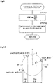
- Figs. 1 to 4 show an optical sensor 1 according to a first embodiment.
- the optical sensor 1 includes a substrate 2, light emitting elements 3 to 5, a light receiving element 6, a signal processing circuit 11, and the like.
- the substrate 2 is a flat plate formed from an insulating material.
- a printed wiring board is used as the substrate 2.
- the light emitting elements 3 to 5 and the light receiving element 6 are mounted on a surface 2A of the substrate 2.
- the light emitting elements 3 to 5 are mounted on the surface 2A of the substrate 2 and emit light such as infrared light or visible light.
- the optical axes of the light emitting elements 3 to 5 generally extend, for example, in a direction perpendicular to the surface 2A of the substrate 2 (in a Z-axis direction).
- LEDs light emitting diodes
- LDs laser diodes
- VCSELs vertical cavity surface emitting lasers
- VCSELs vertical cavity surface emitting lasers
- the three light emitting elements 3 to 5 are disposed on the surface 2A of the substrate 2 so as not to be aligned in a line. Thus, a triangular region TA is formed inside the three light emitting elements 3 to 5 on the surface 2A of the substrate 2.
- the light receiving element 6 is mounted on the surface 2A of the substrate 2 and receives infrared light or visible light.
- a photodiode (PD), a phototransistor, or the like is used as the light receiving element 6.
- the light receiving element 6 is disposed within the triangular region TA on the surface 2A of the substrate 2. It should be noted that the light receiving element 6 may be disposed outside the triangular region TA.
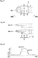
- a transparent resin layer 7 is formed on the surface 2A of the substrate 2.
- the transparent resin layer 7 covers the entirety of the surface 2A of the substrate 2 and seals the light emitting elements 3 to 5 and the light receiving element 6.
- light emitting element lenses 7A to 7C are formed at positions corresponding to the respective light emitting elements 3 to 5.
- the light emitting element lenses 7A to 7C are formed in substantially semispherical shapes projecting upward.
- the centers of the light emitting element lenses 7A to 7C coincide with the mounted positions of the light emitting elements 3 to 5.
- the optical axes of the light beams from the light emitting elements 3 to 5 extend in the Z-axis direction.
- the optical axes of the light beams from the light emitting elements 3 to 5 may be inclined relative to the Z-axis direction by displacing the centers of the light emitting element lenses 7A to 7C and the mounted positions of the light emitting elements 3 to 5 relative to each other. In this case, it is preferred to cause the optical axes of the light beams from the light emitting elements 3 to 5 to extend toward outside the triangular region TA such that later-described phase differences T21 and T32 are increased.
- a light receiving element lens 7D is formed at a position corresponding to the light receiving element 6.
- the light receiving element lens 7D is also formed in a semispherical shape similarly to the light emitting element lenses 7A to 7C.
- the light receiving element lens 7D condenses externally-incident light on the light receiving element 6.
- the light emitting element lenses 7A to 7C and the light receiving element lens 7D are integrally formed in the transparent resin layer 7 which seals the light emitting elements 3 to 5 and the light receiving element 6, but may be provided independently of the transparent resin layer 7.
- the signal processing circuit 11 includes a light emitting element driving portion 12, a light detection signal amplification portion 13, a filter portion 14, and an arithmetic processing portion 15.
- the light emitting element driving portion 12 constitutes a light emission controller together with the arithmetic processing portion 15.
- the light emitting element driving portion 12 is connected to the light emitting elements 3 to 5 and outputs light emission signals St1 to St3 thereto on the basis of a control signal from the arithmetic processing portion 15.
- the light emitting element driving portion 12 supplies driving currents for causing the light emitting elements 3 to 5 to emit light, to the light emitting elements 3 to 5.
- the light detection signal amplification portion 13 is connected to the light receiving element 6, performs current-voltage conversion on a light detection signal S0 supplied from the light receiving element 6, and amplifies the light detection signal S0 on which the current-voltage conversion has been performed.
- the filter portion 14 is connected to a stage subsequent to the light detection signal amplification portion 13 and removes noise from the light detection signal S0 outputted from the light detection signal amplification portion 13.
- the signal processing circuit 11 drives the light emitting elements 3 to 5 by using the light emitting element driving portion 12, and outputs the light detection signal S0 corresponding to reflected light from the detection object Obj, to the arithmetic processing portion 15 by using the light detection signal amplification portion 13 and the filter portion 14.
- the arithmetic processing portion 15 is, for example, a microprocessor and performs a process of controlling light emission of the light emitting elements 3 to 5, a process of separating three reflected light signals Sr1 to Sr3 corresponding to the light emitting elements 3 to 5, from the light detection signal S0, a process of detecting presence or movement of the detection object Obj on the basis of the three reflected light signals Sr1 to Sr3, overall control of the optical sensor 1, and the like.
- the arithmetic processing portion 15 supplies a control signal for controlling the intensity of detection light from and the timing of the light emitting elements 3 to 5, to the light emitting element driving portion 12 to cause the light emitting elements 3 to 5 to emit light so as to correspond to the control signal.
- the light emitting element driving portion 12 supplies pulsed driving currents as the light emission signals St1 to St3 to the light emitting elements 3 to 5, respectively.
- the pulses of the light emission signals St1 to St3 have a constant emission interval T0 and are outputted at different timings for each of the light emitting elements 3 to 5.
- the respective light emitting elements 3 to 5 emit light by pulse emission in a time-division manner (see Fig. 5 ).
- the light emitting elements 3 to 5 may perform pulse emission in a time-division manner. Thus, for example, at the same time as when light emission of the light emitting element 3 is stopped, the next light emission of the light emitting element 4 may be started.
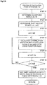
- the arithmetic processing portion 15 executes a program shown in Fig. 6 .
- a movement direction of the detection object Obj is identified by the procedure described below.
- step 1 the arithmetic processing portion 15 reads the light detection signal S0 supplied from the light receiving element 6 via the light detection signal amplification portion 13 and the filter portion 14.
- step 2 the arithmetic processing portion 15 separates the three reflected light signals Sr1 to Sr3 from the light detection signal S0.
- the light emitting elements 3 to 5 emit light in a time-division manner at timings different from each other, reflected light obtained by the detection object Obj reflecting the light from each of the light emitting elements 3 to 5 is received at each of the light emission timings of the light emitting elements 3 to 5.
- the light detection signal S0 it is possible to separate signals of the reflected light based on the light from the respective light emitting elements 3 to 5.
- the arithmetic processing portion 15 extracts the light detection signal S0 at each of the light emission timings of the light emitting elements 3 to 5, and separates the light detection signal S0 into the three reflected light signals Sr1 to Sr3 corresponding to the reflected light of the light emitting elements 3 to 5.
- the reflected light signals Sr1 to Sr3 correspond to signals obtained by performing envelope detection on the pulsed light detection signal S0 extracted at each light emission timing.
- the single light receiving element 6 it is possible to detect the reflected light from the respective light emitting elements 3 to 5.
- the arithmetic processing portion 15 calculates the phase difference T21 between the reflected light signals Sr1 and Sr2, and in step 4, the arithmetic processing portion 15 calculates the phase difference T32 between the reflected light signals Sr2 and Sr3. At that time, the phase differences T21 and T32 are calculated on the basis of the differences among the entire waveforms of the reflected light signals Sr1 to Sr3. Then, in step 5, the arithmetic processing portion 15 identifies the movement direction of the detection object Obj on the basis of these phase differences T21 and T32.
- a start time t0 and an end time t1 of the waveform are determined as a range for calculating the differences among the entire waveforms, on the basis of the reflected light signals Sr1 and Sr2.
- a rise time at which the reflected light signal Sr2 becomes larger than a predetermined threshold is set as the start time t0 and a fall time at which the reflected light signal Sr2 becomes smaller than a predetermined threshold is set as the end time t1.
- start time t0 and the end time t1 are not limited to the above, and may be set, for example, at the rise time and the fall time of the reflected light signal Sr1.
- the start time t0 and the end time t1 may be set on the basis of one of the reflected light signals Sr1 and Sr2 of which the time difference between the rise time and the fall time is larger, or the start time t0 and the end time t1 may be set on the basis of one of the reflected light signals Sr1 and Sr2 of which the time difference between the rise time and the fall time is smaller.
- start time t0 and the end time t1 may be set on the basis of one of the reflected light signals Sr1 and Sr2 of which the rise time is earlier. Moreover, in the case where the size or the movement speed of the detection object Obj is predictable, a time difference between the start time t0 and the end time t1 may previously be set on the basis of the size or the movement speed.
- a maximum value ( ⁇ x0) by which the waveform of the reflected light signal Sr2 is to be shifted to the negative side or the positive side is determined as a detection range of the phase difference T21 on the basis of the reflected light signals Sr1 and Sr2.
- the maximum value ( ⁇ x0) of a shift amount x is set, for example, on the basis of the time difference between the start time t0 and the end time t1 of the waveform of the reflected light signal Sr2.
- the maximum value ( ⁇ x0) of the shift amount may be, for example, a value nearly equal to the time difference between the start time t0 and the end time t1 of the waveform of the reflected light signal Sr2, or may be a value nearly equal to half of the time difference between the start time t0 and the end time t1 of the waveform of the reflected light signal Sr2.
- the maximum value ( ⁇ x0) of the shift amount may be set at a value smaller or larger than the time difference between the start time t0 and the end time t1 of the waveform of the reflected light signal Sr2.
- the maximum value ( ⁇ x0) of the shift amount may be set on the basis of the waveform of the reflected light signal Sr1. If the maximum value ( ⁇ x0) of the shift amount is experimentally predictable, the maximum value ( ⁇ x0) of the shift amount may previously be set at a value based on an experiment.
- step 13 the shift amount x is set at a negative maximum value (-x0) as an initial value.
- step 14 the reflected light signal Sr2 is temporally shifted by the shift amount x using a function Zd1(x) shown in the following mathematical formula 1, and a square sum of the difference between the reflected light signal Sr2 and the reflected light signal Sr1 is calculated in this state.
- the function Zd1(x) calculates the sum of discrete values, but the integral of a continuous value may be calculated.
- the shift amount x is increased by a predetermined value ⁇ x ( ⁇ x > 0), and in step 16, it is determined whether the shift amount x is larger than a positive maximum value (+x0).
- the predetermined value ⁇ x corresponds to an interval at which the phase difference T21 is detected, and is set at a value smaller than the maximum value (+x0).
- step 16 the processes in steps 14 and 15 are repeated.
- step 17 since the shift amount x is larger than the positive maximum value (+x0), the process proceeds to step 17, and a shift amount x21 with which the function Zd1(x) is minimum is outputted as the phase difference T21.
- Steps 21 to 27 for the process of calculating the phase difference T32 are substantially the same as steps 11 to 17 for the process of calculating the phase difference T21.
- a start time t0 and an end time t1 of the waveform are determined as a range for calculating the difference between the entire waveforms, on the basis of the reflected light signals Sr2 and Sr3.
- a maximum value ( ⁇ x0) by which the waveform of the reflected light signal Sr2 is to be shifted to the negative side or the positive side is determined as a detection range of the phase difference T32 on the basis of the reflected light signals Sr2 and Sr3.
- the times t0 and t1 and the maximum value ( ⁇ x0) of a shift amount x that are the same values as those in steps 11 and 12 are set.
- step 23 the shift amount x is set at a negative maximum value (-x0) as an initial value.
- step 24 the reflected light signal Sr3 is temporally shifted by the shift amount x using a function Zd2(x) shown in the following mathematical formula 2, and a square sum of the difference between the reflected light signal Sr3 and the reflected light signal Sr2 is calculated in this state.
- the function Zd2(x) calculates the sum of discrete values, but the integral of a continuous value may be calculated.
- step 25 the shift amount x is increased by a predetermined value ⁇ x ( ⁇ x > 0), and in step 26, it is determined whether the shift amount x is larger than a positive maximum value (+x0). Then, if it is determined as "NO” in step 26, the processes in steps 24 and 25 are repeated. On the other hand, if it is determined as "YES” in step 26, the process proceeds to step 27, and a shift amount x32 with which the function Zd2(x) is minimum is outputted as the phase difference T32.
- the time difference between the start time t0 and the end time t1 as the range of the waveform and the maximum value ( ⁇ x0) that is the range of the shift amount x may be set as large as possible, and the predetermined value ⁇ x may be set as small as possible.
- an increase in calculation amount or a decrease in processing speed occurs as the range of the waveform and the range of the shift amount x are increased and the predetermined value ⁇ x is decreased.
- the range of an integral and the range of the shift amount x are set as small as possible, and the predetermined value ⁇ x is set as large as possible.
- step 31 the ratio f( ⁇ ) between the phase difference T21 and the phase difference T32 is obtained on the basis of an equation in the following mathematical formula 3.
- f ⁇ T 32 T 21
- the movement direction of the detection object Obj is identified by applying the ratio f( ⁇ ) between the phase differences T21 and T32 to a map M shown in Fig. 12 .
- a specific method for creating the map M will be described.
- the case will be considered in which as shown in Fig. 10 , for example, when the light emitting elements 3 to 5 are disposed on the circumference of a circle and a position at the right side of the center of the circumference of the circle is 0°, the light emitting element 3 is disposed at a position of 180°, the light emitting element 4 is disposed at a position of 90°, and the light emitting element 5 is disposed at a position of 0°.
- the movement speed of the detection object Obj is uniform, the detection object Obj moves in a 0° direction, and an angle (rotation angle) when the optical sensor 1 is rotated is ⁇ .
- the distance L21 between the light emitting elements 3 and 4 and the distance L32 between the light emitting elements 4 and 5 in the 0° direction are geometrically changed.
- the relationship is as shown in Fig. 11 . If a classification is made into a case where the distance L21 is positive (L21 > 0) and a case where the distance L21 is negative (L21 ⁇ 0), the angle ⁇ and the ratio f( ⁇ ) correspond to each other in a one-to-one relation. Therefore, it is possible to obtain the angle ⁇ that is the movement direction of the detection object Obj, on the basis of the ratio f( ⁇ ).
- the map M shown in Fig. 12 is a map in which the angle ⁇ is obtained at an interval of 30° in the range of the ratio f( ⁇ ).
- a first threshold f1 at the positive side is the ratio f( ⁇ ) in the case where the angle ⁇ is 165° or 345°
- a first threshold (-f1) at the negative side is the ratio f( ⁇ ) in the case where the angle ⁇ is 105° or 285°.
- a second threshold f2 at the positive side is the ratio f( ⁇ ) in the case where the angle ⁇ is 15° or 195°
- a second threshold (-f2) at the negative side is the ratio f( ⁇ ) in the case where the angle ⁇ is 75° or 255°.
- the case where the light emitting elements 3 to 5 are disposed at predetermined angle positions on the circumference of the circle has been described as an example, but these angle positions may be set as appropriate.
- the light emitting elements 3 to 5 do not necessarily need to be disposed on the circumference of the circle, and may be disposed at any positions on the substrate 2.
- the angle ⁇ may be directly calculated backward using the equation in the mathematical formula 4 without using the map M.
- the light emitting elements 3 to 5 emit light toward above the substrate 2.
- the detection object Obj such as a hand or a finger passes through above the substrate 2 in this state, the optical paths of the light emitting elements 3 to 5 are blocked by the detection object Obj.
- the detection object Obj reflects the light from the light emitting elements 3 to 5.
- the reflected light is received by the light receiving element 6, and the light receiving element 6 outputs a current corresponding to the intensity of the reflected light, as the light detection signal S0.
- the arithmetic processing portion 15 separates the three reflected light signals Sr1 to Sr3 from the light detection signal S0 from the light receiving element 6, and calculates the phase differences T21 and T32 among them. Then, the arithmetic processing portion 15 identifies the movement direction, the position, the movement speed, or the like of the detection object Obj on the basis of the two phase differences T21 and T32.
- the method for identifying the movement direction or the like is as follows.
- a description will be given with a finger as an example of the detection object Obj.
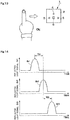
- the detection object Obj moves along the X-axis direction, the detection object Obj passes through above the light emitting elements 3, 4, and 5 in this order.
- peaks of the reflected light signals Sr1, Sr2, and Sr3 occur in this order, and hence the phase differences T21 and T32 also become values corresponding to such an order of occurrence of peaks.
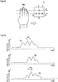
- the magnitudes of the reflected light signals Sr1 to Sr3 change in response to the position of the detection object Obj in the Z-axis direction as shown in Figs. 17 to 19 .
- the detection object Obj when the detection object Obj is located near the optical sensor 1, the reflected light becomes strong, and the reflected light signals Sr1 to Sr3 are also increased.
- the detection object Obj when the detection object Obj is located away from the optical sensor 1, the reflected light becomes weak, and the reflected light signals Sr1 to Sr3 are also decreased.
- the magnitudes of the reflected light signals Sr1 to Sr3 change in response to irregularities of the surface of the detection object Obj.
- the magnitudes of the reflected light signals Sr1 to Sr3 change in response to irregularities such as fingers, so that a plurality of peaks occur in the reflected light signals Sr1 to Sr3.
- the shapes of portions irradiated with the light from the light emitting elements 3 to 5 may be different for each of the light emitting elements 3 to 5.
- the light from the light emitting elements 3 and 5 is applied to four fingers, that is, the index finger, the middle finger, the ring finger, and the little finger.
- the light from the light emitting element 4 is applied to only the three fingers, except for the little finger.
- the reflected light signals Sr1 and Sr3 are different from the reflected light signal Sr2 in number of peaks.
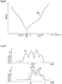
- the peaks, rising, falling, or the like of the reflected light signals Sr1 to Sr3 it may be impossible to obtain precise phase differences T21 and T32.
- the phase differences T21 and T32 are obtained on the basis of the differences among the entire waveforms of the reflected light signals Sr1 to Sr3.
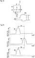
- the relationship between the shift amount x and the function Zd1(x) of the square sum of the difference between the reflected light signals Sr1 and Sr2 is as shown in Fig. 24 .
- the function Zd1(x) has only one minimum value, and thus the shift amount x21 corresponding to the minimum value is detected as the phase difference T21.
- the relationship between the shift amount x and the function Zd2(x) of the square sum of the difference between the reflected light signals Sr2 and Sr3 is as shown in Fig. 26 .
- the function Zd2(x) has two minimum values, but the shift amount x32 corresponding to the smallest minimum value among them is detected as the phase difference T32.
- the reflected light signal Sr3 is shifted by the shift amount x32 as shown by an alternate long and two short dashes line in Fig. 27 , it is recognized that the waveforms of the reflected light signals Sr2 and Sr3 correspond to each other.
- the shift amount x corresponding to the other minimum value corresponds to a position shifted by one finger.
- the waveforms of the reflected light signals Sr1 to Sr3 are different from each other, it is possible to obtain precise phase differences T21 and T32. As a result, it is possible to accurately detect also a movement direction inclined obliquely relative to the X-axis direction and the Y-axis direction, in addition to the X-axis direction and the Y-axis direction.
- steps 1 and 2 in Fig. 6 indicate a specific example of a reflected light signal obtaining unit
- steps 3 and 4 in Fig. 6 indicate a specific example of a phase difference calculator
- step 5 in Fig. 6 indicates a specific example of a movement direction identifying unit.
- phase differences are obtained on the basis of mutual correlations among three reflected light signals. It should be noted that in the second embodiment, the same components as those in the first embodiment are designated by the same reference signs and the description thereof is omitted.
- An optical sensor 21 according to the second embodiment has substantially the same configuration as the optical sensor 1 according to the first embodiment.
- the three light emitting elements 3 to 5 and the light receiving element 6 are provided on the substrate 2, and a signal processing circuit 22 is mounted on the substrate 2.
- the signal processing circuit 22 has substantially the same configuration as the signal processing circuit 11 according to the first embodiment, and includes the light emitting element driving portion 12, the light detection signal amplification portion 13, the filter portion 14, and the arithmetic processing portion 15.
- the arithmetic processing portion 15 according to the second embodiment executes the program shown in Fig. 6 , to identify the movement direction of the detection object Obj.
- the arithmetic processing portion 15 according to the second embodiment obtains the phase differences T21 and T32 on the basis of the mutual correlations among the reflected light signals Sr1 to Sr3.
- a start time t0 and an end time t1 of the waveform are determined as a range for calculating the correlation between the waveforms, on the basis of the reflected light signals Sr1 and Sr2.
- the maximum value ( ⁇ x0) by which the waveform of the reflected light signal Sr2 is to be shifted to the negative side or the positive side is determined as a detection range of the phase difference T21 on the basis of the reflected light signals Sr1 and Sr2.
- a shift amount x is set at a negative maximum value (-x0) as an initial value.
- the reflected light signal Sr2 is temporally shifted by the shift amount x using a function Zc1(x) shown in the following mathematical formula 5, and a product sum of the reflected light signals Sr1 and Sr2 is calculated in this state.
- the function Zc1(x) is a correlation function of the reflected light signals Sr1 and Sr2. It should be noted that the function Zc1(x) calculates the sum of discrete values, but the integral of a continuous value may be calculated.
- step 45 the shift amount x is increased by a predetermined value ⁇ x ( ⁇ x > 0), and in step 46, it is determined whether the shift amount x is larger than a positive maximum value (+x0). Then, if it is determined as "NO” in step 46, the processes in steps 44 and 45 are repeated. On the other hand, if it is determined as "YES” in step 46, the process proceeds to step 47, and a shift amount x21 with which the function Zc1(x) is maximum is outputted as the phase difference T21.
- a start time t0 and an end time t1 of the waveform are determined as a range for calculating the correlation between the waveforms, on the basis of the reflected light signals Sr2 and Sr3.
- a maximum value ( ⁇ x0) by which the waveform of the reflected light signal Sr2 is to be shifted to the negative side or the positive side is determined as a detection range of the phase difference T32 on the basis of the reflected light signals Sr2 and Sr3.
- step 53 the shift amount x is set at a negative maximum value (-x0) as an initial value.
- step 54 the reflected light signal Sr3 is temporally shifted by the shift amount x using a function Zc2(x) shown in the following mathematical formula 6, and a product sum of the reflected light signals Sr2 and Sr3 is calculated in this state.
- the function Zc2(x) is a correlation function of the reflected light signals Sr2 and Sr3. It should be noted that the function Zc2(x) calculates the sum of discrete values, but the integral of a continuous value may be calculated.
- step 55 the shift amount x is increased by a predetermined value ⁇ x ( ⁇ x > 0), and in step 56, it is determined whether the shift amount x is larger than a positive maximum value (+x0). Then, if it is determined as "NO” in step 56, the processes in steps 54 and 55 are repeated. On the other hand, if it is determined as "YES” in step 56, the process proceeds to step 57, and a shift amount x32 with which the function Zc2(x) is maximum is outputted as the phase difference T32.
- steps 43 to 47 in Fig. 28 and steps 53 to 57 in Fig. 29 indicate a specific example of the phase difference calculator.
- a third embodiment of the present invention will be described with reference to Fig. 30 .
- three light receiving elements are provided corresponding to three light emitting elements. It should be noted that in the third embodiment, the same components as those in the first embodiment are designated by the same reference signs and the description thereof is omitted.
- three light receiving elements 32 to 34 are mounted on the substrate 2.
- the light receiving element 32 is located near the light emitting element 3 and receives the reflected light based on the light from the light emitting element 3.
- the light receiving element 33 is located near the light emitting element 4 and receives the reflected light based on the light from the light emitting element 4.
- the light receiving element 34 is located near the light emitting element 5 and receives the reflected light based on the light from the light emitting element 5.
- the light emitting elements 3 to 5 do not need to emit light by pulse emission in a time-division manner, and may continuously emit light.
- light detection signals outputted from the three light receiving elements 32 to 34 correspond to the reflected light signals Sr1 to Sr3, respectively, and thus the three light receiving elements 32 to 34 form a part of the reflected light signal obtaining unit.
- the third embodiment is also applicable to the second embodiment.
- the case of including the three light receiving elements 32 to 34 has been described as an example, but two light receiving elements may be provided, or four or more light receiving elements may be provided.
- the signal processing circuit 11 or 22 is mounted on the substrate 2, but may be provided independently of the substrate 2.
- phase difference T21 between the reflected light signals Sr1 and Sr2 and the phase difference T32 between the reflected light signals Sr2 and Sr3 has been described as an example.
- the present invention is not limited thereto.
- a phase difference T31 between the reflected light signals Sr1 and Sr3 may be used instead of either one of the phase differences T21 and T32, or these three phase differences T21, T32, and T31 may be used.
Landscapes
- Engineering & Computer Science (AREA)
- Physics & Mathematics (AREA)
- General Physics & Mathematics (AREA)
- Theoretical Computer Science (AREA)
- General Engineering & Computer Science (AREA)
- Electromagnetism (AREA)
- Human Computer Interaction (AREA)
- Computer Networks & Wireless Communication (AREA)
- Radar, Positioning & Navigation (AREA)
- Remote Sensing (AREA)
- Geophysics And Detection Of Objects (AREA)
- Length Measuring Devices By Optical Means (AREA)
- Position Input By Displaying (AREA)
Claims (10)
- Optischer Sensor (1, 21, 31), der Folgendes umfasst:ein Substrat (2);wenigstens drei Licht emittierende Elemente (3, 4, 5), die auf einer Oberfläche (2A) des Substrats (2) montiert sind;eine Lichtemissionssteuerung (12), konfiguriert zum Steuern von Lichtemissionsvorgängen der wenigstens drei Licht emittierenden Elemente (3, 4, 5); undwenigstens ein Licht empfangendes Element (6, 32, 33, 34), das auf der Oberfläche (2A) des Substrats (2) montiert ist, wobeiLicht, das durch Reflexion, durch ein Erkennungsobjekt (Obj), von von den Licht emittierenden Elementen (3, 4, 5) emittiertem Licht erhalten wird, von dem Licht empfangenden Element (6, 32, 33, 34) empfangen wird, um dadurch Anwesenheit und Bewegung des Erkennungsobjekts (Obj) zu erkennen, undder optische Sensor (1, 21, 31) Folgendes beinhaltet:eine Reflexionslichtsignaleinholeinheit (13, 14), konfiguriert zum Einholen von drei Reflexionslichtsignalen entsprechend dem Licht von den drei Licht emittierenden Elementen (3, 4, 5) auf der Basis eines von dem Licht empfangenden Element (6, 32, 33, 34) ausgegebenen Lichterkennungssignals (S0), wenn das Licht, das durch Reflexion, durch das Erkennungsobjekt (Obj), des Lichts von den wenigstens drei Licht emittierenden Elementen (3, 4, 5) erhalten wird, von dem Licht empfangenden Element (6, 32, 33, 34) empfangen wird;dadurch gekennzeichnet, dass der optische Sensor (1, 21, 31) Folgendes beinhaltet:einen Phasendifferenzkalkulator, konfiguriert zum Einholen einer Phasendifferenz (T21) auf der Basis von Differenzen oder Korrelationen unter ganzen Wellenformen eines ersten Signals und eines zweiten Signals der drei Reflexionslichtsignale (Sr1, Sr2, Sr3) und einer Phasendifferenz (T32) auf der Basis von Differenzen oder Korrelationen unter ganzen Wellenformen des genannten zweiten Signals und des dritten Signals der drei Reflexionslichtsignale (Sr1, Sr2, Sr3); undeine Bewegungsrichtungsidentifikationseinheit, konfiguriert zum Identifizieren einer Bewegungsrichtung des Erkennungsobjekts (Obj) auf der Basis von wenigstens den zwei Phasendifferenzen (T21, T32),wobei der Phasendifferenzkalkulator beim Berechnen einer Phasendifferenz zwischen zwei Reflexionlichtsignalen (Sr1, Sr2, Sr3) in einem Zustand, in dem eines der Reflexionslichtsignale (Sr1, Sr2, Sr3) zeitlich um einen vorbestimmten Verschiebungsbetrag verschoben wird, ein Quadrat einer Differenz von dem anderen der Reflexionslichtsignale (Sr1, Sr2, Sr3) über die gesamte Wellenform für mehrere Verschiebungsbeträge summiert,und Festlegen eines Verschiebungsbetrags (x21, x32), mit dem der summierte Wert minimal ist, als die Phasendifferenz.
- Optischer Sensor (1,21, 31), der Folgendes umfasst:ein Substrat (2);wenigstens drei Licht emittierende Elemente (3, 4, 5), die auf einer Oberfläche (2A) des Substrats (2) montiert sind;eine Lichtemissionssteuerung (12), konfiguriert zum Steuern von Lichtemissionsvorgängen der wenigstens drei Licht emittierenden Elemente (3, 4, 5); undwenigstens ein Licht empfangendes Element (6, 32, 33, 34), das auf der Oberfläche (2A) des Substrats (2) montiert ist, wobeiLicht, das durch Reflexion, durch ein Erkennungsobjekt (Obj), von von den Licht emittierenden Elementen (3, 4, 5) emittiertem Licht erhalten wird, von dem Licht empfangenden Element (6, 32, 33, 34) empfangen wird, um dadurch Anwesenheit und Bewegung des Erkennungsobjekts (Obj) zu erkennen, undder optische Sensor (1, 21, 31) Folgendes beinhaltet:eine Reflexionslichtsignaleinholeinheit (13, 14), konfiguriert zum Einholen von drei Reflexionslichtsignalen entsprechend dem Licht von den drei Licht emittierenden Elementen (3, 4, 5) auf der Basis eines von dem Licht empfangenden Element (6, 32, 33, 34) ausgegebenen Lichterkennungssignals (S0), wenn das Licht, das durch Reflexion, durch das Erkennungsobjekt (Obj), des Lichts von den wenigstens drei Licht emittierenden Elementen (3, 4, 5) von dem Licht empfangenden Element (6, 32, 33, 34) erhalten wird, empfangen wird;dadurch gekennzeichnet, dass der optische Sensor (1, 21, 31) Folgendes beinhaltet:einen Phasendifferenzkalkulator, konfiguriert zum Einholen einer Phasendifferenz (T21) auf der Basis von Differenzen oder Korrelationen unter ganzen Wellenformen eines ersten Signals und eines zweiten Signals aus den drei reflektierten Lichtsignalen (Sr1, Sr2, Sr3) und einer Phasendifferenz (T32) auf der Basis von Differenzen oder Korrelationen unter ganzen Wellenformen des genannten zweiten Signals und des dritten Signals aus den drei reflektierten Lichtsignalen (Sr1, Sr2, Sr3); undeine Bewegungsrichtungsidentifikationseinheit, konfiguriert zum Identifizieren einer Bewegungsrichtung des Erkennungsobjekts (Obj) auf der Basis von wenigstens den beiden Phasendifferenzen (T21, T32),wobei der Phasendifferenzkalkulator beim Berechnen einer Phasendifferenz zwischen zwei reflektierten Lichtsignalen (Sr1, Sr2, Sr3) für mehrere Verschiebungsbeträge eine Produktsummenberechnung der zwei Reflexionslichtsignale (Sr1, Sr2, Sr3) in einem Zustand durchführt, in dem eines der Reflexionslichtsignale (Sr1, Sr2, Sr3) zeitlich um einen vorbestimmten Verschiebungsbetrag verschoben wird, und einen Verschiebungsbetrag (x21, x32), mit dem der berechnete Wert maximal ist, als Phasendifferenz festlegt.
- Optischer Sensor (1, 21, 31) nach Anspruch 1 oder 2, wobei die Lichtemissionssteuerung (12) bewirkt, dass jedes der wenigstens drei Licht emittierenden Elemente (3, 4, 5) Licht durch Pulsemission auf eine Time-Division-Weise emittiert.
- Optischer Sensor (1, 21, 31) nach einem vorherigen Anspruch, wobei jedes der Licht emittierenden Elemente (3, 4, 5) ein VCSE-(Vertical Cavity Surface Emitting)-Laser ist.
- Optischer Sensor (1, 21, 31) nach einem vorherigen Anspruch, der ferner eine transparente Harzschicht (7) auf der Oberfläche des Substrats (2) umfasst, wobei die transparente Harzschicht (7) die Licht emittierenden Elemente (3, 4, 5) versiegelt.
- Optischer Sensor (1, 21, 31) nach Anspruch 5, wobei die transparente Harzschicht (7) Licht emittierende Elementelinsen (7A, 7B, 7C) an Positionen entsprechend den Licht emittierenden Elementen (3, 4, 5) umfasst.
- Optischer Sensor (1, 21, 31) nach Anspruch 5 oder 6, wobei die transparente Harzschicht (7) eine Licht empfangende Elementelinse (7D) an einer Position entsprechend dem Licht empfangenden Element (6) umfasst.
- Optischer Sensor (1, 21, 31) nach einem vorherigen Anspruch, wobei die Reflexionslichtsignaleinholeinheit (13, 14) ferner zum Einholen der Reflexionslichtsignale (Sr1, Sr2, Sr3) durch Durchführen einer Hüllkurvenerkennung an einem pulsierten Lichterkennungssignal konfiguriert ist.
- Optischer Sensor (1, 21, 31) nach einem vorherigen Anspruch, wobei der Phasendifferenzkalkulator ferner, beim Berechnen der Differenzen unter den ganzen Wellenformen, zum Bestimmen der Startzeit (t0) und der Endzeit (t1) der Wellenform als Bereich konfiguriert ist;
wobei die Startzeit (t0) auf eine Anstiegszeit gesetzt wird, zu der das Reflexionslichtsignal (Sr1, Sr2, Sr3) größer wird als eine vorbestimmte Schwelle; und
wobei die Endzeit (t1) auf eine Abfallzeit gesetzt wird, zu der das Reflexionslichtsignal (Sr1, Sr2, Sr3) kleiner wird als eine vorbestimmte Schwelle. - Optischer Sensor (1, 21, 31) nach Anspruch 9, wobei der Phasendifferenzkalkulator ferner zum Einstellen des Maximalwerts des Verschiebungsbetrags (x21, x32) auf der Basis der Zeitdifferenz zwischen der Startzeit (t0) und der Endzeit (t1) der Wellenform des Reflexionslichtsignals (Sr1, Sr2, Sr3) konfiguriert ist.
Applications Claiming Priority (2)
| Application Number | Priority Date | Filing Date | Title |
|---|---|---|---|
| JP2012061867 | 2012-03-19 | ||
| PCT/JP2013/056107 WO2013141021A1 (ja) | 2012-03-19 | 2013-03-06 | 光センサ |
Publications (3)
| Publication Number | Publication Date |
|---|---|
| EP2829951A1 EP2829951A1 (de) | 2015-01-28 |
| EP2829951A4 EP2829951A4 (de) | 2015-05-06 |
| EP2829951B1 true EP2829951B1 (de) | 2017-11-01 |
Family
ID=49222483
Family Applications (1)
| Application Number | Title | Priority Date | Filing Date |
|---|---|---|---|
| EP13764924.0A Not-in-force EP2829951B1 (de) | 2012-03-19 | 2013-03-06 | Optischer sensor |
Country Status (5)
| Country | Link |
|---|---|
| US (1) | US9476901B2 (de) |
| EP (1) | EP2829951B1 (de) |
| JP (1) | JP5765483B2 (de) |
| CN (1) | CN104205020B (de) |
| WO (1) | WO2013141021A1 (de) |
Families Citing this family (8)
| Publication number | Priority date | Publication date | Assignee | Title |
|---|---|---|---|---|
| JP6607709B2 (ja) * | 2015-06-08 | 2019-11-20 | ローム株式会社 | 近接センサ |
| JP6753653B2 (ja) * | 2015-06-23 | 2020-09-09 | ローム株式会社 | 近接センサ及びそれを用いた電子機器 |
| FR3053136A1 (fr) * | 2016-06-27 | 2017-12-29 | Valeo Comfort & Driving Assistance | Dispositif de detection de gestes |
| FR3053135B1 (fr) * | 2016-06-27 | 2018-08-10 | Valeo Comfort And Driving Assistance | Dispositif de detection de gestes |
| CN110178044B (zh) * | 2017-01-23 | 2022-04-05 | 深圳源光科技有限公司 | 检测装置、检测系统及检测装置的制作方法 |
| TWI662482B (zh) * | 2017-06-28 | 2019-06-11 | 緯創資通股份有限公司 | 手勢識別方法以及手勢識別模組 |
| US11157111B2 (en) * | 2017-08-29 | 2021-10-26 | Sony Interactive Entertainment LLC | Ultrafine LED display that includes sensor elements |
| AT522115B1 (de) * | 2019-01-24 | 2024-12-15 | Zactrack Gmbh | Bühnentechnische Vorrichtung und Verfahren zur Bestimmung einer Korrelationsfunktion |
Family Cites Families (17)
| Publication number | Priority date | Publication date | Assignee | Title |
|---|---|---|---|---|
| JP3240941B2 (ja) * | 1996-11-18 | 2001-12-25 | 松下電器産業株式会社 | 手振り検出方法及び装置 |
| JP2891955B2 (ja) * | 1997-02-14 | 1999-05-17 | 日本電気移動通信株式会社 | Lcd表示装置 |
| WO2002037410A1 (en) * | 2000-11-06 | 2002-05-10 | Koninklijke Philips Electronics N.V. | Method of measuring the movement of an input device. |
| WO2005076116A2 (en) * | 2004-02-09 | 2005-08-18 | Koninklijke Philips Electronics N.V. | Optical input device based on doppler shift and laser self-mixing |
| JP2007003355A (ja) * | 2005-06-23 | 2007-01-11 | Shinku Rei:Kk | パルス光伝播時間計測装置および仮想マウス等の応用装置 |
| JP2007104567A (ja) * | 2005-10-07 | 2007-04-19 | Sharp Corp | 電子機器 |
| US20070080940A1 (en) * | 2005-10-07 | 2007-04-12 | Sharp Kabushiki Kaisha | Remote control system, and display device and electronic device using the remote control system |
| US8253768B2 (en) * | 2005-12-09 | 2012-08-28 | Ricoh Company, Ltd. | Optical scanner and image forming apparatus |
| JP4912071B2 (ja) * | 2006-08-04 | 2012-04-04 | 株式会社リコー | 光走査装置、光走査方法、画像形成装置、カラー画像形成装置、プログラム、記録媒体 |
| EP2068212A1 (de) * | 2007-12-06 | 2009-06-10 | The Swatch Group Research and Development Ltd. | Tragbarer Gegenstand wie etwa ein Uhrwerk, der Elemente zum Einschalten einer elektronischen Steuerfunktion umfasst |
| US9869689B2 (en) * | 2009-04-29 | 2018-01-16 | Koninklijke Philips Electronics N.V. | Laser diode based multiple-beam laser spot imaging system for characterization of vehicle dynamics |
| US8619029B2 (en) * | 2009-05-22 | 2013-12-31 | Motorola Mobility Llc | Electronic device with sensing assembly and method for interpreting consecutive gestures |
| US8810524B1 (en) * | 2009-11-20 | 2014-08-19 | Amazon Technologies, Inc. | Two-sided touch sensor |
| JP2011227574A (ja) | 2010-04-15 | 2011-11-10 | Rohm Co Ltd | 演算装置、動き検出装置、電子機器 |
| JP5758688B2 (ja) * | 2010-07-22 | 2015-08-05 | ローム株式会社 | 照明機器 |
| KR101146454B1 (ko) | 2010-07-29 | 2012-05-18 | 엘지엔시스(주) | 매체의 자기성분 검출방법 및 그를 이용한 매체인식방법과 매체인식장치 |
| JP2012173029A (ja) * | 2011-02-18 | 2012-09-10 | Seiko Epson Corp | 光学式位置検出装置および入力機能付き表示システム |
-
2013
- 2013-03-06 WO PCT/JP2013/056107 patent/WO2013141021A1/ja not_active Ceased
- 2013-03-06 JP JP2014506127A patent/JP5765483B2/ja not_active Expired - Fee Related
- 2013-03-06 EP EP13764924.0A patent/EP2829951B1/de not_active Not-in-force
- 2013-03-06 CN CN201380015398.XA patent/CN104205020B/zh not_active Expired - Fee Related
-
2014
- 2014-09-18 US US14/489,543 patent/US9476901B2/en not_active Expired - Fee Related
Non-Patent Citations (1)
| Title |
|---|
| None * |
Also Published As
| Publication number | Publication date |
|---|---|
| JPWO2013141021A1 (ja) | 2015-08-03 |
| WO2013141021A1 (ja) | 2013-09-26 |
| JP5765483B2 (ja) | 2015-08-19 |
| EP2829951A4 (de) | 2015-05-06 |
| CN104205020B (zh) | 2016-12-28 |
| US20150006106A1 (en) | 2015-01-01 |
| US9476901B2 (en) | 2016-10-25 |
| EP2829951A1 (de) | 2015-01-28 |
| CN104205020A (zh) | 2014-12-10 |
Similar Documents
| Publication | Publication Date | Title |
|---|---|---|
| EP2829951B1 (de) | Optischer sensor | |
| KR101891907B1 (ko) | 거리 측정 장치 및 시차 연산 시스템 | |
| JP6805504B2 (ja) | 距離測定装置、移動体装置及び距離測定方法 | |
| US10444331B1 (en) | 3D camera system and method for detecting abnormal state of beam projector module for eye protection | |
| CN106324586B (zh) | 光子设备 | |
| US20080204700A1 (en) | Method For Light Propagation Time Measurement | |
| EP3279691B1 (de) | Entfernungsmesser basiert auf parallaxenberechnung | |
| EP3859391B1 (de) | Näherungsdetektionsvorrichtung | |
| JP2014182028A (ja) | 限定領域反射型光電センサ | |
| WO2016143482A1 (ja) | 光学式検知装置 | |
| KR20140145481A (ko) | 차량용 tof 카메라 | |
| EP3667360A1 (de) | Optische vorrichtung | |
| EP2829958B1 (de) | Optischer sensor | |
| US10085013B2 (en) | 3D camera module | |
| WO2013015145A1 (ja) | 情報取得装置および物体検出装置 | |
| EP4525436A1 (de) | Kamera | |
| JP2005195416A (ja) | 測距センサおよびこれを備えた電子機器 | |
| EP3069167B1 (de) | Verfahren zur beleuchtung eines objekts und zur bestimmung einer entfernung | |
| JP2004003995A (ja) | 基板検出センサ | |
| KR20200041851A (ko) | 카메라 장치 | |
| JP2019168235A (ja) | 走査装置及び測距装置 |
Legal Events
| Date | Code | Title | Description |
|---|---|---|---|
| PUAI | Public reference made under article 153(3) epc to a published international application that has entered the european phase |
Free format text: ORIGINAL CODE: 0009012 |
|
| 17P | Request for examination filed |
Effective date: 20140915 |
|
| AK | Designated contracting states |
Kind code of ref document: A1 Designated state(s): AL AT BE BG CH CY CZ DE DK EE ES FI FR GB GR HR HU IE IS IT LI LT LU LV MC MK MT NL NO PL PT RO RS SE SI SK SM TR |
|
| AX | Request for extension of the european patent |
Extension state: BA ME |
|
| RA4 | Supplementary search report drawn up and despatched (corrected) |
Effective date: 20150407 |
|
| RIC1 | Information provided on ipc code assigned before grant |
Ipc: G06F 3/03 20060101ALI20150330BHEP Ipc: G01S 17/58 20060101ALI20150330BHEP Ipc: G01P 13/04 20060101ALI20150330BHEP Ipc: G06F 3/042 20060101ALI20150330BHEP Ipc: G06F 3/01 20060101ALI20150330BHEP Ipc: G06F 3/041 20060101ALI20150330BHEP Ipc: G06F 3/0346 20130101AFI20150330BHEP |
|
| DAX | Request for extension of the european patent (deleted) | ||
| RIC1 | Information provided on ipc code assigned before grant |
Ipc: G06F 3/01 20060101ALI20170322BHEP Ipc: G01S 17/58 20060101ALI20170322BHEP Ipc: G06F 3/03 20060101ALI20170322BHEP Ipc: G06F 3/042 20060101ALI20170322BHEP Ipc: G06F 3/0346 20130101AFI20170322BHEP Ipc: G06F 3/041 20060101ALI20170322BHEP Ipc: G01P 13/04 20060101ALI20170322BHEP |
|
| GRAP | Despatch of communication of intention to grant a patent |
Free format text: ORIGINAL CODE: EPIDOSNIGR1 |
|
| INTG | Intention to grant announced |
Effective date: 20170511 |
|
| GRAS | Grant fee paid |
Free format text: ORIGINAL CODE: EPIDOSNIGR3 |
|
| GRAA | (expected) grant |
Free format text: ORIGINAL CODE: 0009210 |
|
| AK | Designated contracting states |
Kind code of ref document: B1 Designated state(s): AL AT BE BG CH CY CZ DE DK EE ES FI FR GB GR HR HU IE IS IT LI LT LU LV MC MK MT NL NO PL PT RO RS SE SI SK SM TR |
|
| REG | Reference to a national code |
Ref country code: GB Ref legal event code: FG4D |
|
| REG | Reference to a national code |
Ref country code: CH Ref legal event code: EP Ref country code: AT Ref legal event code: REF Ref document number: 942649 Country of ref document: AT Kind code of ref document: T Effective date: 20171115 |
|
| REG | Reference to a national code |
Ref country code: IE Ref legal event code: FG4D |
|
| REG | Reference to a national code |
Ref country code: DE Ref legal event code: R096 Ref document number: 602013028785 Country of ref document: DE |
|
| REG | Reference to a national code |
Ref country code: NL Ref legal event code: MP Effective date: 20171101 |
|
| REG | Reference to a national code |
Ref country code: LT Ref legal event code: MG4D |
|
| REG | Reference to a national code |
Ref country code: AT Ref legal event code: MK05 Ref document number: 942649 Country of ref document: AT Kind code of ref document: T Effective date: 20171101 |
|
| PG25 | Lapsed in a contracting state [announced via postgrant information from national office to epo] |
Ref country code: SE Free format text: LAPSE BECAUSE OF FAILURE TO SUBMIT A TRANSLATION OF THE DESCRIPTION OR TO PAY THE FEE WITHIN THE PRESCRIBED TIME-LIMIT Effective date: 20171101 Ref country code: FI Free format text: LAPSE BECAUSE OF FAILURE TO SUBMIT A TRANSLATION OF THE DESCRIPTION OR TO PAY THE FEE WITHIN THE PRESCRIBED TIME-LIMIT Effective date: 20171101 Ref country code: LT Free format text: LAPSE BECAUSE OF FAILURE TO SUBMIT A TRANSLATION OF THE DESCRIPTION OR TO PAY THE FEE WITHIN THE PRESCRIBED TIME-LIMIT Effective date: 20171101 Ref country code: NO Free format text: LAPSE BECAUSE OF FAILURE TO SUBMIT A TRANSLATION OF THE DESCRIPTION OR TO PAY THE FEE WITHIN THE PRESCRIBED TIME-LIMIT Effective date: 20180201 Ref country code: NL Free format text: LAPSE BECAUSE OF FAILURE TO SUBMIT A TRANSLATION OF THE DESCRIPTION OR TO PAY THE FEE WITHIN THE PRESCRIBED TIME-LIMIT Effective date: 20171101 Ref country code: ES Free format text: LAPSE BECAUSE OF FAILURE TO SUBMIT A TRANSLATION OF THE DESCRIPTION OR TO PAY THE FEE WITHIN THE PRESCRIBED TIME-LIMIT Effective date: 20171101 |
|
| PG25 | Lapsed in a contracting state [announced via postgrant information from national office to epo] |
Ref country code: HR Free format text: LAPSE BECAUSE OF FAILURE TO SUBMIT A TRANSLATION OF THE DESCRIPTION OR TO PAY THE FEE WITHIN THE PRESCRIBED TIME-LIMIT Effective date: 20171101 Ref country code: AT Free format text: LAPSE BECAUSE OF FAILURE TO SUBMIT A TRANSLATION OF THE DESCRIPTION OR TO PAY THE FEE WITHIN THE PRESCRIBED TIME-LIMIT Effective date: 20171101 Ref country code: LV Free format text: LAPSE BECAUSE OF FAILURE TO SUBMIT A TRANSLATION OF THE DESCRIPTION OR TO PAY THE FEE WITHIN THE PRESCRIBED TIME-LIMIT Effective date: 20171101 Ref country code: BG Free format text: LAPSE BECAUSE OF FAILURE TO SUBMIT A TRANSLATION OF THE DESCRIPTION OR TO PAY THE FEE WITHIN THE PRESCRIBED TIME-LIMIT Effective date: 20180201 Ref country code: RS Free format text: LAPSE BECAUSE OF FAILURE TO SUBMIT A TRANSLATION OF THE DESCRIPTION OR TO PAY THE FEE WITHIN THE PRESCRIBED TIME-LIMIT Effective date: 20171101 Ref country code: GR Free format text: LAPSE BECAUSE OF FAILURE TO SUBMIT A TRANSLATION OF THE DESCRIPTION OR TO PAY THE FEE WITHIN THE PRESCRIBED TIME-LIMIT Effective date: 20180202 Ref country code: IS Free format text: LAPSE BECAUSE OF FAILURE TO SUBMIT A TRANSLATION OF THE DESCRIPTION OR TO PAY THE FEE WITHIN THE PRESCRIBED TIME-LIMIT Effective date: 20180301 |
|
| PG25 | Lapsed in a contracting state [announced via postgrant information from national office to epo] |
Ref country code: CZ Free format text: LAPSE BECAUSE OF FAILURE TO SUBMIT A TRANSLATION OF THE DESCRIPTION OR TO PAY THE FEE WITHIN THE PRESCRIBED TIME-LIMIT Effective date: 20171101 Ref country code: SK Free format text: LAPSE BECAUSE OF FAILURE TO SUBMIT A TRANSLATION OF THE DESCRIPTION OR TO PAY THE FEE WITHIN THE PRESCRIBED TIME-LIMIT Effective date: 20171101 Ref country code: CY Free format text: LAPSE BECAUSE OF FAILURE TO SUBMIT A TRANSLATION OF THE DESCRIPTION OR TO PAY THE FEE WITHIN THE PRESCRIBED TIME-LIMIT Effective date: 20171101 Ref country code: EE Free format text: LAPSE BECAUSE OF FAILURE TO SUBMIT A TRANSLATION OF THE DESCRIPTION OR TO PAY THE FEE WITHIN THE PRESCRIBED TIME-LIMIT Effective date: 20171101 Ref country code: DK Free format text: LAPSE BECAUSE OF FAILURE TO SUBMIT A TRANSLATION OF THE DESCRIPTION OR TO PAY THE FEE WITHIN THE PRESCRIBED TIME-LIMIT Effective date: 20171101 |
|
| REG | Reference to a national code |
Ref country code: DE Ref legal event code: R097 Ref document number: 602013028785 Country of ref document: DE |
|
| PG25 | Lapsed in a contracting state [announced via postgrant information from national office to epo] |
Ref country code: RO Free format text: LAPSE BECAUSE OF FAILURE TO SUBMIT A TRANSLATION OF THE DESCRIPTION OR TO PAY THE FEE WITHIN THE PRESCRIBED TIME-LIMIT Effective date: 20171101 Ref country code: SM Free format text: LAPSE BECAUSE OF FAILURE TO SUBMIT A TRANSLATION OF THE DESCRIPTION OR TO PAY THE FEE WITHIN THE PRESCRIBED TIME-LIMIT Effective date: 20171101 Ref country code: PL Free format text: LAPSE BECAUSE OF FAILURE TO SUBMIT A TRANSLATION OF THE DESCRIPTION OR TO PAY THE FEE WITHIN THE PRESCRIBED TIME-LIMIT Effective date: 20171101 Ref country code: IT Free format text: LAPSE BECAUSE OF FAILURE TO SUBMIT A TRANSLATION OF THE DESCRIPTION OR TO PAY THE FEE WITHIN THE PRESCRIBED TIME-LIMIT Effective date: 20171101 |
|
| PLBE | No opposition filed within time limit |
Free format text: ORIGINAL CODE: 0009261 |
|
| STAA | Information on the status of an ep patent application or granted ep patent |
Free format text: STATUS: NO OPPOSITION FILED WITHIN TIME LIMIT |
|
| 26N | No opposition filed |
Effective date: 20180802 |
|
| REG | Reference to a national code |
Ref country code: CH Ref legal event code: PL |
|
| GBPC | Gb: european patent ceased through non-payment of renewal fee |
Effective date: 20180306 |
|
| PG25 | Lapsed in a contracting state [announced via postgrant information from national office to epo] |
Ref country code: SI Free format text: LAPSE BECAUSE OF FAILURE TO SUBMIT A TRANSLATION OF THE DESCRIPTION OR TO PAY THE FEE WITHIN THE PRESCRIBED TIME-LIMIT Effective date: 20171101 Ref country code: MC Free format text: LAPSE BECAUSE OF FAILURE TO SUBMIT A TRANSLATION OF THE DESCRIPTION OR TO PAY THE FEE WITHIN THE PRESCRIBED TIME-LIMIT Effective date: 20171101 |
|
| REG | Reference to a national code |
Ref country code: BE Ref legal event code: MM Effective date: 20180331 |
|
| REG | Reference to a national code |
Ref country code: IE Ref legal event code: MM4A |
|
| PG25 | Lapsed in a contracting state [announced via postgrant information from national office to epo] |
Ref country code: LU Free format text: LAPSE BECAUSE OF NON-PAYMENT OF DUE FEES Effective date: 20180306 |
|
| PG25 | Lapsed in a contracting state [announced via postgrant information from national office to epo] |
Ref country code: IE Free format text: LAPSE BECAUSE OF NON-PAYMENT OF DUE FEES Effective date: 20180306 |
|
| PG25 | Lapsed in a contracting state [announced via postgrant information from national office to epo] |
Ref country code: GB Free format text: LAPSE BECAUSE OF NON-PAYMENT OF DUE FEES Effective date: 20180306 Ref country code: BE Free format text: LAPSE BECAUSE OF NON-PAYMENT OF DUE FEES Effective date: 20180331 Ref country code: LI Free format text: LAPSE BECAUSE OF NON-PAYMENT OF DUE FEES Effective date: 20180331 Ref country code: CH Free format text: LAPSE BECAUSE OF NON-PAYMENT OF DUE FEES Effective date: 20180331 |
|
| PG25 | Lapsed in a contracting state [announced via postgrant information from national office to epo] |
Ref country code: FR Free format text: LAPSE BECAUSE OF NON-PAYMENT OF DUE FEES Effective date: 20180331 |
|
| PG25 | Lapsed in a contracting state [announced via postgrant information from national office to epo] |
Ref country code: MT Free format text: LAPSE BECAUSE OF NON-PAYMENT OF DUE FEES Effective date: 20180306 |
|
| PG25 | Lapsed in a contracting state [announced via postgrant information from national office to epo] |
Ref country code: TR Free format text: LAPSE BECAUSE OF FAILURE TO SUBMIT A TRANSLATION OF THE DESCRIPTION OR TO PAY THE FEE WITHIN THE PRESCRIBED TIME-LIMIT Effective date: 20171101 |
|
| PG25 | Lapsed in a contracting state [announced via postgrant information from national office to epo] |
Ref country code: PT Free format text: LAPSE BECAUSE OF FAILURE TO SUBMIT A TRANSLATION OF THE DESCRIPTION OR TO PAY THE FEE WITHIN THE PRESCRIBED TIME-LIMIT Effective date: 20171101 Ref country code: HU Free format text: LAPSE BECAUSE OF FAILURE TO SUBMIT A TRANSLATION OF THE DESCRIPTION OR TO PAY THE FEE WITHIN THE PRESCRIBED TIME-LIMIT; INVALID AB INITIO Effective date: 20130306 |
|
| PG25 | Lapsed in a contracting state [announced via postgrant information from national office to epo] |
Ref country code: MK Free format text: LAPSE BECAUSE OF NON-PAYMENT OF DUE FEES Effective date: 20171101 |
|
| PG25 | Lapsed in a contracting state [announced via postgrant information from national office to epo] |
Ref country code: AL Free format text: LAPSE BECAUSE OF FAILURE TO SUBMIT A TRANSLATION OF THE DESCRIPTION OR TO PAY THE FEE WITHIN THE PRESCRIBED TIME-LIMIT Effective date: 20171101 |
|
| PGFP | Annual fee paid to national office [announced via postgrant information from national office to epo] |
Ref country code: DE Payment date: 20210319 Year of fee payment: 9 |
|
| REG | Reference to a national code |
Ref country code: DE Ref legal event code: R119 Ref document number: 602013028785 Country of ref document: DE |
|
| PG25 | Lapsed in a contracting state [announced via postgrant information from national office to epo] |
Ref country code: DE Free format text: LAPSE BECAUSE OF NON-PAYMENT OF DUE FEES Effective date: 20221001 |