EP2829511B1 - Device comprising a fluid channel having at least one micro or nanoelectronic system and method for producing such a device - Google Patents
Device comprising a fluid channel having at least one micro or nanoelectronic system and method for producing such a device Download PDFInfo
- Publication number
- EP2829511B1 EP2829511B1 EP14177849.8A EP14177849A EP2829511B1 EP 2829511 B1 EP2829511 B1 EP 2829511B1 EP 14177849 A EP14177849 A EP 14177849A EP 2829511 B1 EP2829511 B1 EP 2829511B1
- Authority
- EP
- European Patent Office
- Prior art keywords
- layer
- sealing
- substrate
- microelectronic
- fluid channel
- Prior art date
- Legal status (The legal status is an assumption and is not a legal conclusion. Google has not performed a legal analysis and makes no representation as to the accuracy of the status listed.)
- Active
Links
- 239000012530 fluid Substances 0.000 title claims description 116
- 238000004519 manufacturing process Methods 0.000 title description 29
- 101100460147 Sarcophaga bullata NEMS gene Proteins 0.000 claims description 118
- 238000007789 sealing Methods 0.000 claims description 109
- 239000000758 substrate Substances 0.000 claims description 100
- 238000000034 method Methods 0.000 claims description 45
- 239000000463 material Substances 0.000 claims description 44
- 238000004377 microelectronic Methods 0.000 claims description 42
- 238000005530 etching Methods 0.000 claims description 32
- 239000002184 metal Substances 0.000 claims description 31
- 239000004065 semiconductor Substances 0.000 claims description 19
- 230000005496 eutectics Effects 0.000 claims description 12
- XUIMIQQOPSSXEZ-UHFFFAOYSA-N Silicon Chemical compound [Si] XUIMIQQOPSSXEZ-UHFFFAOYSA-N 0.000 claims description 11
- 238000007906 compression Methods 0.000 claims description 10
- 229920000642 polymer Polymers 0.000 claims description 9
- 238000000926 separation method Methods 0.000 claims description 9
- 238000005520 cutting process Methods 0.000 claims description 7
- 239000011521 glass Substances 0.000 claims description 7
- 239000011324 bead Substances 0.000 claims description 6
- 239000011810 insulating material Substances 0.000 claims description 6
- 229910052581 Si3N4 Inorganic materials 0.000 claims description 5
- 238000007650 screen-printing Methods 0.000 claims description 5
- HQVNEWCFYHHQES-UHFFFAOYSA-N silicon nitride Chemical compound N12[Si]34N5[Si]62N3[Si]51N64 HQVNEWCFYHHQES-UHFFFAOYSA-N 0.000 claims description 5
- 238000004817 gas chromatography Methods 0.000 claims description 4
- 238000001465 metallisation Methods 0.000 claims description 4
- 238000005096 rolling process Methods 0.000 claims description 4
- 238000003776 cleavage reaction Methods 0.000 claims description 3
- 229910010272 inorganic material Inorganic materials 0.000 claims description 3
- 239000011147 inorganic material Substances 0.000 claims description 3
- 239000011368 organic material Substances 0.000 claims description 3
- 230000007017 scission Effects 0.000 claims description 3
- -1 oxides Substances 0.000 claims description 2
- 229910000449 hafnium oxide Inorganic materials 0.000 claims 1
- WIHZLLGSGQNAGK-UHFFFAOYSA-N hafnium(4+);oxygen(2-) Chemical compound [O-2].[O-2].[Hf+4] WIHZLLGSGQNAGK-UHFFFAOYSA-N 0.000 claims 1
- 239000010410 layer Substances 0.000 description 228
- 238000007306 functionalization reaction Methods 0.000 description 63
- 239000010408 film Substances 0.000 description 43
- 229910052751 metal Inorganic materials 0.000 description 30
- 238000000151 deposition Methods 0.000 description 17
- KRHYYFGTRYWZRS-UHFFFAOYSA-N Fluorane Chemical compound F KRHYYFGTRYWZRS-UHFFFAOYSA-N 0.000 description 12
- 230000008021 deposition Effects 0.000 description 12
- 229910052710 silicon Inorganic materials 0.000 description 11
- 238000005498 polishing Methods 0.000 description 10
- 239000010703 silicon Substances 0.000 description 10
- 230000008569 process Effects 0.000 description 9
- VYPSYNLAJGMNEJ-UHFFFAOYSA-N Silicium dioxide Chemical compound O=[Si]=O VYPSYNLAJGMNEJ-UHFFFAOYSA-N 0.000 description 8
- 230000015572 biosynthetic process Effects 0.000 description 8
- 239000003989 dielectric material Substances 0.000 description 8
- 229910052814 silicon oxide Inorganic materials 0.000 description 8
- 230000008901 benefit Effects 0.000 description 7
- 238000005229 chemical vapour deposition Methods 0.000 description 7
- 238000000206 photolithography Methods 0.000 description 7
- 239000011347 resin Substances 0.000 description 7
- 229920005989 resin Polymers 0.000 description 7
- 239000000126 substance Substances 0.000 description 7
- 239000007788 liquid Substances 0.000 description 5
- 238000004518 low pressure chemical vapour deposition Methods 0.000 description 5
- 238000000623 plasma-assisted chemical vapour deposition Methods 0.000 description 5
- 239000011241 protective layer Substances 0.000 description 5
- BOTDANWDWHJENH-UHFFFAOYSA-N Tetraethyl orthosilicate Chemical compound CCO[Si](OCC)(OCC)OCC BOTDANWDWHJENH-UHFFFAOYSA-N 0.000 description 4
- 238000000407 epitaxy Methods 0.000 description 4
- 239000000203 mixture Substances 0.000 description 4
- BLRPTPMANUNPDV-UHFFFAOYSA-N Silane Chemical compound [SiH4] BLRPTPMANUNPDV-UHFFFAOYSA-N 0.000 description 3
- 229910021417 amorphous silicon Inorganic materials 0.000 description 3
- 238000000231 atomic layer deposition Methods 0.000 description 3
- 238000010292 electrical insulation Methods 0.000 description 3
- 238000005538 encapsulation Methods 0.000 description 3
- 230000008020 evaporation Effects 0.000 description 3
- 238000001704 evaporation Methods 0.000 description 3
- 230000003993 interaction Effects 0.000 description 3
- 150000002739 metals Chemical class 0.000 description 3
- 239000012071 phase Substances 0.000 description 3
- 239000011148 porous material Substances 0.000 description 3
- 229910000077 silane Inorganic materials 0.000 description 3
- 229910016570 AlCu Inorganic materials 0.000 description 2
- 229910015365 Au—Si Inorganic materials 0.000 description 2
- IERHLVCPSMICTF-XVFCMESISA-N CMP group Chemical group P(=O)(O)(O)OC[C@@H]1[C@H]([C@H]([C@@H](O1)N1C(=O)N=C(N)C=C1)O)O IERHLVCPSMICTF-XVFCMESISA-N 0.000 description 2
- 239000004593 Epoxy Substances 0.000 description 2
- ISWSIDIOOBJBQZ-UHFFFAOYSA-N Phenol Chemical compound OC1=CC=CC=C1 ISWSIDIOOBJBQZ-UHFFFAOYSA-N 0.000 description 2
- OAICVXFJPJFONN-UHFFFAOYSA-N Phosphorus Chemical compound [P] OAICVXFJPJFONN-UHFFFAOYSA-N 0.000 description 2
- 241000724291 Tobacco streak virus Species 0.000 description 2
- NIXOWILDQLNWCW-UHFFFAOYSA-N acrylic acid group Chemical group C(C=C)(=O)O NIXOWILDQLNWCW-UHFFFAOYSA-N 0.000 description 2
- 229910052782 aluminium Inorganic materials 0.000 description 2
- XAGFODPZIPBFFR-UHFFFAOYSA-N aluminium Chemical compound [Al] XAGFODPZIPBFFR-UHFFFAOYSA-N 0.000 description 2
- 239000005380 borophosphosilicate glass Substances 0.000 description 2
- 239000013317 conjugated microporous polymer Substances 0.000 description 2
- CJNBYAVZURUTKZ-UHFFFAOYSA-N hafnium(iv) oxide Chemical compound O=[Hf]=O CJNBYAVZURUTKZ-UHFFFAOYSA-N 0.000 description 2
- 239000012212 insulator Substances 0.000 description 2
- 239000007791 liquid phase Substances 0.000 description 2
- 210000003643 myeloid progenitor cell Anatomy 0.000 description 2
- 230000003071 parasitic effect Effects 0.000 description 2
- 239000002245 particle Substances 0.000 description 2
- 229910052698 phosphorus Inorganic materials 0.000 description 2
- 239000011574 phosphorus Substances 0.000 description 2
- 239000005360 phosphosilicate glass Substances 0.000 description 2
- 238000001020 plasma etching Methods 0.000 description 2
- 229920001296 polysiloxane Polymers 0.000 description 2
- 238000002360 preparation method Methods 0.000 description 2
- 230000009467 reduction Effects 0.000 description 2
- 230000035945 sensitivity Effects 0.000 description 2
- 238000005245 sintering Methods 0.000 description 2
- 241000894007 species Species 0.000 description 2
- 239000010409 thin film Substances 0.000 description 2
- 230000002463 transducing effect Effects 0.000 description 2
- 239000012808 vapor phase Substances 0.000 description 2
- ZOXJGFHDIHLPTG-UHFFFAOYSA-N Boron Chemical compound [B] ZOXJGFHDIHLPTG-UHFFFAOYSA-N 0.000 description 1
- 229910000673 Indium arsenide Inorganic materials 0.000 description 1
- 229910004298 SiO 2 Inorganic materials 0.000 description 1
- 229910000577 Silicon-germanium Inorganic materials 0.000 description 1
- 241000897276 Termes Species 0.000 description 1
- 240000008042 Zea mays Species 0.000 description 1
- 239000000853 adhesive Substances 0.000 description 1
- 230000001070 adhesive effect Effects 0.000 description 1
- 239000004411 aluminium Substances 0.000 description 1
- 238000005280 amorphization Methods 0.000 description 1
- 238000004458 analytical method Methods 0.000 description 1
- 238000013459 approach Methods 0.000 description 1
- 229910052796 boron Inorganic materials 0.000 description 1
- 150000001722 carbon compounds Chemical class 0.000 description 1
- 238000004587 chromatography analysis Methods 0.000 description 1
- 150000001875 compounds Chemical class 0.000 description 1
- 230000006835 compression Effects 0.000 description 1
- 239000004020 conductor Substances 0.000 description 1
- 238000000708 deep reactive-ion etching Methods 0.000 description 1
- 238000001514 detection method Methods 0.000 description 1
- 238000010586 diagram Methods 0.000 description 1
- 238000006073 displacement reaction Methods 0.000 description 1
- 238000009826 distribution Methods 0.000 description 1
- 230000000694 effects Effects 0.000 description 1
- 238000005516 engineering process Methods 0.000 description 1
- 238000011049 filling Methods 0.000 description 1
- 230000014509 gene expression Effects 0.000 description 1
- 229910052732 germanium Inorganic materials 0.000 description 1
- 238000000227 grinding Methods 0.000 description 1
- 238000010438 heat treatment Methods 0.000 description 1
- RPQDHPTXJYYUPQ-UHFFFAOYSA-N indium arsenide Chemical compound [In]#[As] RPQDHPTXJYYUPQ-UHFFFAOYSA-N 0.000 description 1
- 238000001764 infiltration Methods 0.000 description 1
- 230000008595 infiltration Effects 0.000 description 1
- 238000010030 laminating Methods 0.000 description 1
- 238000003698 laser cutting Methods 0.000 description 1
- 239000006193 liquid solution Substances 0.000 description 1
- 238000001459 lithography Methods 0.000 description 1
- 230000000873 masking effect Effects 0.000 description 1
- 239000011159 matrix material Substances 0.000 description 1
- 229910003465 moissanite Inorganic materials 0.000 description 1
- 230000003287 optical effect Effects 0.000 description 1
- 238000004806 packaging method and process Methods 0.000 description 1
- 238000002161 passivation Methods 0.000 description 1
- 238000003825 pressing Methods 0.000 description 1
- 230000001902 propagating effect Effects 0.000 description 1
- 239000010453 quartz Substances 0.000 description 1
- 238000011084 recovery Methods 0.000 description 1
- 229910010271 silicon carbide Inorganic materials 0.000 description 1
- LIVNPJMFVYWSIS-UHFFFAOYSA-N silicon monoxide Chemical class [Si-]#[O+] LIVNPJMFVYWSIS-UHFFFAOYSA-N 0.000 description 1
- XUIMIQQOPSSXEZ-NJFSPNSNSA-N silicon-30 atom Chemical compound [30Si] XUIMIQQOPSSXEZ-NJFSPNSNSA-N 0.000 description 1
- 238000001179 sorption measurement Methods 0.000 description 1
- 239000007921 spray Substances 0.000 description 1
- 238000009718 spray deposition Methods 0.000 description 1
- 238000004381 surface treatment Methods 0.000 description 1
- 229920001187 thermosetting polymer Polymers 0.000 description 1
- 238000000427 thin-film deposition Methods 0.000 description 1
- 238000011282 treatment Methods 0.000 description 1
- 238000001039 wet etching Methods 0.000 description 1
Images


Classifications
-
- G—PHYSICS
- G01—MEASURING; TESTING
- G01N—INVESTIGATING OR ANALYSING MATERIALS BY DETERMINING THEIR CHEMICAL OR PHYSICAL PROPERTIES
- G01N30/00—Investigating or analysing materials by separation into components using adsorption, absorption or similar phenomena or using ion-exchange, e.g. chromatography or field flow fractionation
- G01N30/02—Column chromatography
- G01N30/60—Construction of the column
- G01N30/6095—Micromachined or nanomachined, e.g. micro- or nanosize
-
- B—PERFORMING OPERATIONS; TRANSPORTING
- B81—MICROSTRUCTURAL TECHNOLOGY
- B81C—PROCESSES OR APPARATUS SPECIALLY ADAPTED FOR THE MANUFACTURE OR TREATMENT OF MICROSTRUCTURAL DEVICES OR SYSTEMS
- B81C1/00—Manufacture or treatment of devices or systems in or on a substrate
- B81C1/00015—Manufacture or treatment of devices or systems in or on a substrate for manufacturing microsystems
- B81C1/00023—Manufacture or treatment of devices or systems in or on a substrate for manufacturing microsystems without movable or flexible elements
- B81C1/00119—Arrangement of basic structures like cavities or channels, e.g. suitable for microfluidic systems
-
- B—PERFORMING OPERATIONS; TRANSPORTING
- B01—PHYSICAL OR CHEMICAL PROCESSES OR APPARATUS IN GENERAL
- B01D—SEPARATION
- B01D53/00—Separation of gases or vapours; Recovering vapours of volatile solvents from gases; Chemical or biological purification of waste gases, e.g. engine exhaust gases, smoke, fumes, flue gases, aerosols
- B01D53/02—Separation of gases or vapours; Recovering vapours of volatile solvents from gases; Chemical or biological purification of waste gases, e.g. engine exhaust gases, smoke, fumes, flue gases, aerosols by adsorption, e.g. preparative gas chromatography
-
- B—PERFORMING OPERATIONS; TRANSPORTING
- B81—MICROSTRUCTURAL TECHNOLOGY
- B81C—PROCESSES OR APPARATUS SPECIALLY ADAPTED FOR THE MANUFACTURE OR TREATMENT OF MICROSTRUCTURAL DEVICES OR SYSTEMS
- B81C1/00—Manufacture or treatment of devices or systems in or on a substrate
- B81C1/00015—Manufacture or treatment of devices or systems in or on a substrate for manufacturing microsystems
- B81C1/00261—Processes for packaging MEMS devices
- B81C1/00269—Bonding of solid lids or wafers to the substrate
-
- G—PHYSICS
- G01—MEASURING; TESTING
- G01N—INVESTIGATING OR ANALYSING MATERIALS BY DETERMINING THEIR CHEMICAL OR PHYSICAL PROPERTIES
- G01N30/00—Investigating or analysing materials by separation into components using adsorption, absorption or similar phenomena or using ion-exchange, e.g. chromatography or field flow fractionation
- G01N30/02—Column chromatography
- G01N30/62—Detectors specially adapted therefor
- G01N30/64—Electrical detectors
-
- B—PERFORMING OPERATIONS; TRANSPORTING
- B81—MICROSTRUCTURAL TECHNOLOGY
- B81B—MICROSTRUCTURAL DEVICES OR SYSTEMS, e.g. MICROMECHANICAL DEVICES
- B81B2201/00—Specific applications of microelectromechanical systems
- B81B2201/05—Microfluidics
- B81B2201/058—Microfluidics not provided for in B81B2201/051 - B81B2201/054
-
- B—PERFORMING OPERATIONS; TRANSPORTING
- B81—MICROSTRUCTURAL TECHNOLOGY
- B81C—PROCESSES OR APPARATUS SPECIALLY ADAPTED FOR THE MANUFACTURE OR TREATMENT OF MICROSTRUCTURAL DEVICES OR SYSTEMS
- B81C2203/00—Forming microstructural systems
- B81C2203/01—Packaging MEMS
- B81C2203/0172—Seals
-
- H—ELECTRICITY
- H01—ELECTRIC ELEMENTS
- H01L—SEMICONDUCTOR DEVICES NOT COVERED BY CLASS H10
- H01L2924/00—Indexing scheme for arrangements or methods for connecting or disconnecting semiconductor or solid-state bodies as covered by H01L24/00
- H01L2924/10—Details of semiconductor or other solid state devices to be connected
- H01L2924/146—Mixed devices
- H01L2924/1461—MEMS
Definitions
- the present invention relates to a device comprising a fluid channel provided with at least one micro or nanoelectronic system and to a method for producing such a device.
- microelectronic or nanoelectronic systems integrate microelectromechanical systems or MEMS (microelectromechanical systems in English) and nanoelectromechanical systems or NEMS (Nanoelectromechanical systems). For the sake of simplification, they will be named in the rest of the MEMS and NEMS description. These systems are currently widely used in many products. New applications appear in particular due to the development of NEMS which offer new advantages thanks to the reduction of dimensions. In particular, due to the high mass sensitivity of this type of system, they are of great interest for chemical or biological sensors.
- a NEMS or MEMS has a fixed part and at least one suspended part (which can be mobile) or sensitive part relative to the fixed part
- the MEMS or NEMS type structure which offers particular physicochemical characteristics, to a surrounding medium, generally gaseous or liquid.
- the MEMS or NEMS sensitive structure is placed in a fluid channel in which the medium flows and allows the medium to be analyzed to be brought into contact with the NEMS or MEMS sensitive structure.
- the fluid channel is produced by attaching a cover to a substrate comprising the sensitive structure or structures.
- the cover is sealed on the substrate and has at least two openings to ensure the circulation in the channel of the fluid to be analyzed.
- the cover is formed by a cavity made in a substrate of several ⁇ m to several hundred ⁇ m deep for example.
- the document WO2011 / 154363 describes an analysis device, for example a gas chromatography microcolumn comprising MEMS and / or NEMS in the microcolumn, forming sensors.
- the connection of MEMS and / or NEMS is carried out for example by vias.
- the cover seal may be of the polymer seal, molecular seal, anode seal, eutectic seal, glass sintering, etc. type.
- One technique consists, after sealing the cover, of opening large cavities in the thickness of the cover only above the areas of metallized pads to allow direct contact recovery by wirebonding on these pads, each contact pad being surrounded by a sealing bead, for example made of polymer, to isolate this part of the cavity.
- this technique has the drawback of introducing additional patterns for these electrical passages inside the fluid channel, which is undesirable since they can cause disturbance of the circulation of the fluid, generation of dead volumes, etc.
- this technique is ill-suited in the case of sensitive structures of the NEMS or MEMS type because these structures require contact pads made of semiconductor material or small metal to reduce the parasitic capacitances and be able to extract an exploitable electrical signal with a good signal / noise ratio.
- this technique is not suitable for components formed of NEMS or MEMS in networks, because these are interconnected with one another with a high density, which implies the implementation very small studs, and possibly using several metal levels.
- TSV Through Silicon Via in English
- TGV Through Glass Via in English
- 3D MEMS high vaccum wafer level packaging S. Nicolas et al. Electronic Components and Technology Conference (ECTC), 2012 IEEE 62nd, Date of Conference: May 29 2012-June 1 2012 , describes such achievements.
- TSV type connections would for example be made in the thickness of the cover and would open into the cavity, the electrical continuity then being ensured by a stud / metal cord inside the cavity.
- the document FR2957535 describes a microfluidic system comprising a substrate and a cover produced by overmolding on a flow sensor.
- This system comprises a sensitive part and a fluid channel defined between the substrate and the cover, the microelectronic structure being located inside the fluid channel.
- a structure comprising a fluid channel formed by a substrate comprising at least one sensitive structure, at at least one electrical connection between the sensitive structure and an area outside the fluid channel, said electrical connection being formed on the surface of the substrate carrying the sensitive structure, an intermediate layer covering at least partially the electrical connection, said intermediate layer having a free face suitable for sealing the cover, and a cover sealed in a sealed manner on the flat free face of the intermediate layer.
- face of the intermediate layer suitable for sealing means a face having a surface state allowing sealing with the base faces of the cover, for example a dry film seal, a molecular seal, eutectic or by thermocompression.
- the face suitable for sealing may have a certain roughness or a certain relief which nevertheless allows sealing.
- an intermediate layer allows the realization of lateral connection lines while ensuring a simplified realization of the sealing between the cover and the substrate, since the sealing is carried out on the advantageously flat intermediate layer.
- connection or connections being made on the surface of the substrate and covered by the intermediate layer, they do not disturb the flow unlike the other solutions mentioned above, for example TSVs made in the cover.
- the fluid channel device includes a layer ensuring encapsulation of the connection lines at least in the sealing zone with the cover, this layer then allows the release of the NEMS / MEMS structure while retaining a surface allowing the sealing above the connection lines, this surface being sufficiently flat to effect a tight sealing of the cover on the NEMS / MEMS structure.
- the invention therefore makes it possible not to resort to the production of via through the cover and / or to the opening of large cavities in the thickness of the cover to allow contact to be resumed.
- the production process is therefore considerably simplified.
- this intermediate layer can be such that it encapsulates the materials of the NEMS or MEMS structure except the sensitive part which, due to their presence in the fluid channel, could interact with the medium circulating in the channel, ie it isolates the materials of the NEMS or MEMS structure other than the sensitive part of the interior of the fluid channel.
- This is the case for example with metals or dielectrics which are used in the fluid channel if the mechanical structure consists of a dense network of NEMS.
- the intermediate layer is only open at the level of the NEMS structures intended to interact with the surrounding medium.
- the presence of the intermediate layer allows the release of the mechanical structures before the sealing of the cover.
- layers of functionalization of the various mechanical structures implemented other than by the liquid route are much more compatible with released mechanical structures. They can be implemented, for example by vapor phase deposits or by evaporation, epitaxy or any other method of formation, or even of layer transfer. Thanks to the invention, it is possible to deposit a functionalization layer on the NEMS or MEMS structure and thus to functionalize them before sealing the cover on the substrate carrying the mechanical structures. In this case, the functionalization layer can completely cover the suspended part of the mechanical structures, thus offering an increased interaction surface between the environment and the functionalization layer.
- a dry resin film is used to seal the NEMS part comprising the intermediate layer and the cover.
- the structure according to the invention and its production method allows a collective production of chips provided with a fluid channel, the chips being separated by pre-sawing between the channels and precut transverse to the channels.
- the present invention therefore relates to a device comprising a substrate comprising at least one microelectronic and / or nanoelectronic structure comprising at least one sensitive part and a fluid channel defined between said substrate and a cover, said fluid channel comprising two lateral walls and one wall.
- said device also comprising an intermediate layer comprising a face in contact with base faces of said side walls, said face of the intermediate layer having a sealability with the base faces, said connection line being at least partially covered by said intermediate layer at least directly above the face of base of said side wall, said side walls being tightly secured to said s ubstrate by sealing on said intermediate layer.
- the device comprising at least one pair of connection lines extending laterally on either side of the microelectronic and / or nanoelectronic structure and each passing under a side wall.
- the intermediate layer covers, in the fluid channel, the entire microelectronic and / or nanoelectronic structure with the exception of its sensitive part.
- the intermediate layer may include an electrical insulating material, such as a silicon oxide, or a silicon nitride.
- the device comprises a functionalization layer encapsulating at least part of the sensitive part of the microelectronic and / or nanoelectronic structure.
- the functionalization layer can comprise one or more materials chosen from organic or inorganic materials, polymers, oxides, semiconductors.
- the functionalization layer (s) may be produced by chemical vapor deposition, by evaporation, epitaxy, porosification by etching, spray deposition, spotting (deposition of drops), etc. It is particularly advantageous to use porous materials as a functionalization layer.
- the device may include connection lines and contact pads, said contact pads being located outside the fluid channel, said connection lines extending between the microelectronic and / or nanoelectronic structure and the contact pads.
- connection lines comprise several metallization levels at least inside the channel.
- the sealing can advantageously be carried out by means of a dry sealing film interposed between the intermediate layer and the base faces of the side walls of the cover.
- the dry film is preferably a resin with epoxy, phenol, acrylic or silicone bases for example.
- the dry sealing film can be structured in several beads at the interfaces between the intermediate layer and the base faces of the side walls.
- the cords are substantially parallel to the fluid channel.
- the device can also comprise at least one layer of material interposed between the intermediate layer and the base faces of the side walls performing a eutectic sealing, by thermo-compression, by screen printing or a sealing by sintering of glass.
- the seal can also be a molecular seal, no interposition of material between the cover and the intermediate layer is then required.
- the intermediate layer comprises a first layer of electrical insulating material in contact with the connection line and a second layer (deposited on the first layer, said second layer being of a material such that it is little or not sensitive to a step of releasing the microelectronic and / or nanoelectronic structure.
- the first layer has a flat face on which the second layer is deposited.
- the second layer is for example made of Si, silicon nitride, metal (AISi, AlCu, ...) or Hafnium oxide (HfO2) ... This first layer is advantageously planarizing.
- the channel forms a gas chromatography microcolumn.
- the layer is, according to an advantageous mode, deposited and then structured to be eliminated above all or part of the sensitive parts of the MEMS / NEMS structures.
- Step c) can be carried out at any time during the process, provided that this is before step d).
- the method may include, after step b), a step of releasing said microelectronic and / or nanoelectronic structure.
- the production method may also include a step of producing a functionalization layer inside the fluid channel on the microelectronic and / or nanoelectronic structure and / or on the walls of the cover and / or on the intermediate layer, said step being performed before sealing.
- the functionalization layer can be formed before the release of the sensitive part, or even before the formation of the sensitive structure.
- Functionalization layers at different locations in the fluid channel can be deposited, in this case, these layers can be of the same nature or not.
- Heating can also be applied when applying pressure.
- the preparation can be a plasma type treatment.
- the intermediate layer can be produced by depositing a first layer of electrical insulating material and depositing a second layer on the first layer.
- the material of the second layer is preferably chosen to have little or no sensitivity to the step of releasing the microelectronic and / or nanoelectronic structure, when this method includes a release step.
- the seal is a eutectic seal or by thermo-compression, or by molecular seal or by screen printing.
- the release can be obtained by etching using hydrofluoric acid vapor.
- said substrate can comprise several microelectronic and / or nanoelectronic structures and the cover substrate comprising several covers, the covers being sealed simultaneously on the substrate comprising the microelectronic and / or nanoelectronic structures, so that a fluid channel of a device may or may not communicate with the fluid channel of other devices.
- the fluid channels of line devices can communicate with one another while the fluid channels of column devices are arranged one next to the other.
- the separation of the devices is carried out for example by cleavage.
- the cover substrate may include cavities formed beforehand between the channels in which the contact pads are located after sealing, the method may also include a step of cutting the cover substrate to open said cavities. This step can be carried out before or after the cuts or precuts to separate the devices.
- said method may include the step of removing by etching the functionalization layer on the contact pads after sealing and opening the cavities in the cover, said covers forming masks in this etching for microelectronic and / or nanoelectronic structures.
- NEMS / MEMS is understood to mean a mechanical structure comprising a fixed structure and at least one sensitive structure and means for actuating and / or transducing at least one characteristic of the sensitive structure.
- the sensitive structure can be a suspended mechanical structure and include means for actuating and / or transducing the mechanical movement. Electrical connections are provided to connect the mechanical structure to the outside environment.
- This MEMS / NEMS part can include a network of NEMS and / or MEMS structures, possibly with several metallization levels to achieve the required interconnections. For simplicity, a MEMS or NEMS will be designated by NEMS.
- the device comprises a fluid channel 2, which is rectilinear with axis X in the example shown.
- the fluid channel 2 is delimited by a substrate 4 and a cover 6 transferred to the substrate 4.
- the flow in the fluid channel takes place from one longitudinal end 2.1 to the other 2.2 of the fluid channel 2.
- the cover 6 is formed from a substrate in which a cavity 5 has been formed.
- the cavity 5 delimits with the substrate carrying the NEMS / MEMS structure the fluid channel 2 which ensures the circulation and the distribution of a gaseous or liquid mixture.
- the channel is delimited by two side walls 6.1, an upper bottom 6.2 connecting the two side walls 6.1 and a lower bottom formed by the substrate 4.
- the side walls 6.1 have base faces which allow the cover to be sealed on the substrate.
- inlet end and / or the outlet end of the fluid channel could for example be made in the upper bottom 6.2 of the channel or also in the substrate 4.
- the cover 6 could have a more complex shape, for example this could include a long channel of optimized shape, for example in a spiral, making it possible to produce a chromatography column ensuring the separation function of the compounds of a mixture, the column integrating a NEMS / MEMS structure.
- the substrate comprises a NEMS / MEMS structure 7 located inside the fluid channel 2.
- the NEMS / MEMS structure comprises three NEMS aligned along the longitudinal axis X.
- the device also includes electrical connection lines 8 extending laterally between the NEMS located in the fluid channel 2 and pads 9 located outside the fluid channel.
- the pads 9 are for example made directly in the semiconductor material of the NEMS ⁇ MEMS structure. They can advantageously be covered with metal to ensure good electrical contact.
- the connection lines 8 can be of doped semiconductor of the type of that forming the NEMS / MEMS structure.
- connection lines 8 are separated by trenches 11 so as to electrically isolate the connection lines 8 from each other.
- connection lines 8 can be made with one or more levels of metal separated by a dielectric material as will be described below.
- These lines can also be made of semiconductor covered with metal in order to reduce the electrical resistance of the line.
- connection lines can be made of metal, the contact between the semiconductor in which the structure is made and the metal then being located either in the fluid channel, or outside this channel, or possibly under the sealing zone separating the fluid channel from the outside.
- connection lines 8 comprise a reduced part made of semiconductor material alone to limit the electrical resistances and the parasitic capacitances which can degrade the performance of the NEMS components.
- the metal tracks for forming the connection lines are preferably produced in a damascene configuration to avoid the formation of interstices or voids or zones of lower density in the filling dielectric and in the material of the intermediate layer, which is likely to lead to undesirable infiltration and etching during the step of releasing the mechanical structures, including laterally under the sealing zones between the substrate and the cover. In addition, they could lead to lateral leaks out of the fluid channel.
- three pairs of electrical connection lines 8 extending laterally on either side of the fluid channel 2 are provided by NEMS.
- a device comprising at least two lateral connection lines extending on the same side with respect to the axis X is not beyond the scope of the present invention.
- the suspended structure of the NEMS is formed by a beam 10 embedded at one of its longitudinal ends, for example two gauges 12, for example piezoresistive, are used to detect the displacement of the beam 10.
- two gauges 12 for example piezoresistive
- the substrate 4 comprises a stack of a sacrificial layer 14 used for the production of the NEMS, of a layer 16 of semiconductor in which the fixed part and the mobile part of the NEMS are produced.
- connection lines 8 are formed both in the layer 16 and of a metal line 18 covering the layer 16.
- An intermediate layer 20 at least partially covers the connection lines 8 and a sealing layer 22 is disposed between the intermediate layer 20 and the cover 6.
- the intermediate layer 20 is present at least at the sealing interface between the NEMS / MEMS structure 7 and the cover and is absent from the areas of the NEMS / MEMS structure in order to leave the part or parts part of the NEMS / structure. MEMS suspended in contact with the medium present in the fluid channel.
- the intermediate layer 20 is located only close to the sealing interface between the NEMS / MEMS structure 7 and the cover 6, and more particularly between the connection lines 8 and the cover 6.
- the intermediate layer 20 has a first face 20.1 in contact with the connection lines 8, this face 20.1 according to the topology of the connection lines 8 and of the substrate 4 and a second face 20.2 in contact with the cover 6.
- the intermediate layer 20 is such that the second face 20.2 is capable of carrying out the sealing of the cover 6 comprising the NEMS part, by ensuring both the sealing along the fluid channel and the passage of the connection lines 8 and this in a simplified manner.
- the presence of the intermediate layer 20 makes it possible to compensate for the topology generated by the prior formation of the NEMS / MEMS structure and of the connection lines 8.
- the intermediate layer 20 allows the passage of at least part of the electrical interconnections between the interior of the fluid channel 2 and the exterior of the fluid channel 2 while ensuring a relatively flat sealing interface facilitating the obtaining a seal.
- the intermediate layer 20 has electrical insulation properties so as to electrically insulate the connection lines 8 between them.
- its material is chosen so as to allow obtaining a face 20.2 sufficiently flat for sealing.
- the state of surface of the face 20.2 obtained directly after the deposition of the intermediate layer may be sufficient, or a planarization step is carried out, for example a mechanical-chemical polishing step after the formation of the intermediate layer.
- the material of the intermediate layer is chosen able to be etched, for example in anisotropic etching.
- the material of the intermediate layer 20 is chosen so as to have good selectivity for etching compared to the process for releasing mechanical structures and not to generate a residue during this step.
- the material of the intermediate layer is also chosen so as to be compatible with the materials used for the final assembly of the device between the substrate carrying the NEMS / MEMS structure and the cover.
- the material of the intermediate layer is chosen to be compatible with that of the functionalization layer, in particular so as to ensure good adhesion of the latter.
- the material of the intermediate layer is a dielectric material, for example a silicon oxide, such as for example SiO 2 or an oxide formed from silane or an oxide formed from tetraethylorthosilicate (TEOS), an oxide LTO type silicon (Low Temperature Oxide) formed by low pressure chemical vapor deposition or LPCVD (Low Pressure Chemical Vapor Deposition) undoped or doped with phosphorus (PSG: phospho-Silicate-Glass) or doped with Boron and Phosphorus (BPSG: Boro-Phospho-Silicate Glass), an oxide deposited by chemical vapor deposition assisted by plasma or PECVD (Plasma Enhanced Chemical Vapor Deposition).
- a silicon oxide such as for example SiO 2 or an oxide formed from silane or an oxide formed from tetraethylorthosilicate (TEOS)
- LPCVD Low Pressure Chemical Vapor Deposition
- PSG phospho-Silicate-Glass
- BPSG Boro-P
- the intermediate layer 20 comprises several materials, each having properties involved in the production of the device.
- these materials can be arranged in successive layers.
- the intermediate layer comprises two layers, a first layer deposited on the connection lines, designated planarizing layer, which makes it possible to fill the topology of the NEMS / MEMS structure and the connection lines while ensuring electrical insulation, and a second layer deposited on the first layer intended to increase the protection of the assembly during the step of releasing the mechanical structure.
- the flatness of the planarizing layer ensures the flatness of the protective layer.
- the material of the first layer is made of silicon oxide and the material of the second layer is made of amorphous silicon or any other material capable of holding the release by hydrofluoric acid in the case where the sacrificial layer is made of silicon oxide, such as a metal, silicon nitride, etc. which protects the upper surface of the first oxide layer upon release.
- This embodiment in at least one planarizing layer and a protective layer is particularly advantageous, since the etching speeds of the silicon oxides forming the planarizing layer are generally much higher, for example at least 10 times higher, than the etching speed of the oxide layer of an SOI substrate, for example, which is carried out when the mobile structure (s) are released. In the absence of such a protective layer, the release etching of the mobile structure or structures could cause significant consumption of the planarizing layer.
- This embodiment in two layers therefore advantageously makes it possible to reduce the thickness of the planarizing layer. For example, its thickness can be a few tens of nm.
- the intermediate layer comprises only one material
- its thickness is determined to take account of the consumption of material during the release etching.
- the thickness of the intermediate layer is for example of the order of a few ⁇ m.
- the sealing is carried out by means of a dry resin film 22 or DFR (Dry Film Resist in English).
- a thin film of resin 22 is applied by rolling on the underside of the cover 6 intended to come into contact with the intermediate layer 20 and is structured by photolithography.
- the cover and resin film assembly is transferred and sealed on the intermediate layer 20.
- the thin film 22 is in the form of two parallel beads, having substantially the same sealing surface. These cords are obtained after exposure and development of the dry film.
- the dry film is for example a resin with epoxy, phenol, acrylic or silicone bases for example.
- the dry film has for example a thickness of between a few ⁇ m to several tens of ⁇ m, or even a few hundred ⁇ m with a multilayer of dry film, advantageously only a few ⁇ m to avoid interaction between the material of this sealing bead with the medium. propagating in the fluid channel.
- a seal by another technique does not depart from the scope of the present invention, for example it could be a molecular seal, a eutectic seal, a heat-compression seal, or a seal by serigraphy ....
- the implementation of these techniques may prove to be more complex than sealing with a dry film.
- it will be preferable to limit the temperatures used so as not to deteriorate the metal tracks already present and possibly the functionalization layer.
- these temperatures will be chosen to be less than approximately 400 ° C. to at least preserve the metallic layers of the connection lines. They will be even lower to preserve certain functionalization layers, for example of the polymer type.
- this deposition and this possible structuring are preferably carried out on the hood.
- a layer of Au is preferably deposited on the cover.
- the deposition on the NEMS / MEMS structure is carried out before the release of the structure.
- the material of this layer is then chosen to be compatible with the process of releasing the NEMS / MEMS structure so that it is not etched during this technological step which takes place just before sealing.
- a layer of Au will then be used for example on the cover and on the intermediate layer for an Au-Au sealing, in the case of release of the NEMS with hydrofluoric acid in the vapor phase.
- the device comprises a functionalization layer 24 covering the intermediate layer 20 and the entire NEMS / MEMS structure.
- This functionalization layer 24 is said to be non-localized.
- the functionalization layer surrounds the NEMS structure.
- the term “functionalization layer” is understood to mean a layer present on the surface of the mechanical structure to provide it with specific properties.
- the functionalization layer makes it possible to increase the adsorption of gaseous species in a possibly selective manner or, in the case of a biological sensor, the functionalization layer makes it possible to ensure the grafting of biological species.
- the functionalization layer 24 is for example formed from one or more organic or inorganic materials, polymers, oxides, carbon compounds, semiconductors or other porous materials ...
- the invention very advantageously makes it possible to carry out the step of depositing the functionalization layer on an already released mechanical structure, which makes it possible to almost completely encapsulate the mechanical structure with the functionalization layer ( figure 2B ' ) when the deposit thereof is sufficiently compliant.
- the functionalization layer then has an increased interaction surface with the surrounding medium, which further increases the advantage of a functionalization layer.
- the invention allows the implementation of functionalization layers on NEMS released by contactless and collective techniques, for example by CVD deposition, LPCVD, PECVD, ALD, epitaxy, porosification, etc. and then continue by closing the component by adding a cover comprising a cavity so as to form the fluid channel. Thus the risks of sticking by deposition of the functionalization layer by deposition in the liquid phase are avoided.
- the sealing is carried out by means of a dry film 22 as described above, in fact the temperature of such a sealing is compatible with the presence of a functionalization layer deposited or formed itself at low temperature , e.g. polymer, etc.
- dry film sealing has the advantage of being less demanding in terms of the necessary surface condition (flatness, roughness, presence of particles) at the sealing interface than molecular or eutectic type seals or even by thermo-compression. Thus it allows sealing even in the presence of a functionalization layer at the sealing interface between the intermediate layer and the cover.
- the functionalization layer 224 is produced only on the suspended part of the NEMS, the functionalization layer is then designated localized layer. In this example, the functionalization layer is not present at the level of the sealing zone. On the figure 2C ' , the functionalization layer 224 surrounds the NEMS structure.
- the sealing interface 26 is formed by the face of the cover and the face of the substrate to be sealed.
- the faces to come into contact are prepared in a manner known to those skilled in the art, for example by chemical mechanical polishing (or CMP (chemical-mechanical polishing) in English), ie the face 20.2 of the intermediate layer and the underside of the cover 6.
- CMP chemical-mechanical polishing
- a molecular seal in the presence of a functionalization layer at the interface, the functionalization layer being deposited after release, is also conceivable.
- the sealing interface is formed of a layer of one or more materials, it may be a layer of Au-Si, AIGe or AuGe ... for example in the case of an eutectic sealing, of Au-Au, AuSn ... for example in the case of a sealing by thermo-compression or of adhesives in the case of a sealing by screen printing.
- the sealing is carried out by a sealing interface 26 between the intermediate layer 20 and the cover 6, the device not comprising a functionalization layer.
- the device comprises a non-localized functionalization layer, the sealing is obtained by means of a sealing interface 26 between the functionalization layer 24 and the cover 6.
- the device comprises a localized functionalization layer 224 on the suspended part 10, the sealing is obtained by means of a sealing interface between the intermediate layer 20 and the cover 6.
- the intermediate layer 120 covers both the connection lines at the level of the sealing zone but also the interior of the encapsulating fluid channel thus the NEMS / NEMS structure except the part of this structure intended to be in contact with the surrounding medium, ie generally the suspended part 10.
- the intermediate layer 120 is brought as close as possible to the sensitive parts of the MEMS / NEMS structures and thus forms a channel substantially parallel to the fluid channel.
- the intermediate layer 120 completely covers the MEMS / NEMS structures except the sensitive parts and thus simply forms an opening above the sensitive parts.
- the intermediate layer 120 encapsulates the lines of connection 8 between the different NEMS of the network located in the fluid channel 2.
- This encapsulation has the advantage of isolating the materials involved on the NEMS part which, by their presence in the fluid channel 2, could interact with the medium circulating in the canal. This is the case, for example, with metals or dielectrics which are generally used in the fluid channel if the mechanical structure consists of a dense network of NEMS.
- a fluid channel device in which the intermediate layer would not entirely cover the part of the NEMS / MEMS structure not intended to come into contact with the surrounding medium does not depart from the scope of the present invention.
- This encapsulation by the intermediate layer is particularly advantageous to implement in the case of NEMS networks which are connected together by conductive semiconductor or metal tracks with possibly several levels of interconnections, the electrical insulation between the levels being provided by layers of dielectrics, and the assembly being located in the fluid channel.
- This exemplary embodiment is represented on the Figures 4A and 4B , with two metal levels for the interconnections between NEMS located in the fluid channel and a metal level for the electrical connection with the exterior of the fluid channel.
- This device comprising several NEMS arranged laterally in the conduit.
- three pairs of NEMS are aligned along the X axis.
- Interconnection lines 108.1 are then made on several metal levels, two in the example shown, in order to connect together the NEMS / MEMS structures constituting the network from NEMS, which is located inside the fluid channel.
- Interconnection lines 108.2 are also made (with a single level in the example shown) to connect the NEMS network with the outside of the fluid channel. These lines are not shown on the figure 4A but are on the figure 4B .
- two suspended parts are shown diagrammatically, which corresponds to a section CC ′ of the structure shown in the figure 4A .
- the different metallization levels are partially encapsulated in an electrically insulating layer 230, for example of oxide.
- the interconnections 108.1 between the NEMS comprise two levels of metal and the interconnections 108.2 for connecting the network of NEMS outside the fluid channel comprises a level of metal.
- Interconnections 108.1 and 108.2 with one or more than two levels of metal are not outside the scope of the present invention.
- This device comprises an intermediate layer 220 deposited on the interconnection lines 108.1 and 108.2 apart from the parts 10 intended to interact with the surrounding environment.
- the substrate provided with the NEMS / MEMS structure is produced from a silicon on insulator or SOI substrate (Silicon in Insulator in English) for example.
- any substrate may be used comprising a layer in which the NEMS / MEMS structure would be produced, this layer being formed on a sacrificial layer allowing, by its etching, release of the NEMS / MEMS structure.
- the material of the layer in which the NEMS / MEMS structure is produced can be a monocrystalline or polycrystalline semiconductor, for example Si, Ge, SiGe, SiC, GAAs, InAs, InP ...
- the sacrificial layer can be present on the 'the entire substrate or be located only in certain places where the NEMS will be carried out.
- the NEMS / MEMS structure includes an optical function so as to include opto-electro-mechanical microsystems (or MOEMS, for Micro-Opto-Electro-Mechanical Systems in English) and / or integrate an integrated electronic part , CMOS, etc.
- opto-electro-mechanical microsystems or MOEMS, for Micro-Opto-Electro-Mechanical Systems in English
- MOEMS Micro-Opto-Electro-Mechanical Systems in English
- the SOI substrate comprises a layer of insulating material 28, for example silicon oxide and a layer of silicon 30.
- the silicon in layer 30 is doped.
- the NEMS structures and the semiconductor interconnection lines are produced.
- Photolithography and then anisotropic etching of the silicon layer 30 are carried out in a known manner.
- the structure thus obtained is represented on the figure 6B .
- the structure comprises a plurality of NEMS in the direction X.
- the structure can also comprise several NEMS in the direction Y.
- the metal connection lines are made.
- a deposition of a dielectric layer 32 on the structured layer 30 then takes place, it is for example an oxide formed based on silane SiH 4 whose thickness is greater than the topology of the silicon layer 30 structured.
- a mechanical-chemical or CMP polishing step then takes place in order to make the surface of the layer 32 plane.
- a photolithography of “countermask” type and a partial etching of the layer 30 of the height of the topology to be caught are carried out, which facilitates the polishing step and makes it possible to reduce its duration.
- the layer 32 is opened by photolithography to reach the silicon layer 30 and prepare the making of the electrical contacts.
- a layer of metal 34 is deposited, for example in AISi, the latter having the advantage of offering good resistance to etching by hydrofluoric acid vapor which takes place to release the mechanical structures.
- the metallic layer 34 is etched ( figure 6F ).
- the intermediate layer 20 has two layers.
- a layer of dielectric material 35 forming the planarizing layer is deposited.
- the planarizing layer is for example an oxide formed on the basis of silane SiH 4 , or alternatively an oxide formed on the basis of tetraethylorthosilicate (TEOS).
- TEOS tetraethylorthosilicate
- a protective layer 36 for example of amorphous Si, of silicon nitride, of metal (AISi, AlCu, etc.), of Hafnium oxide (HfO2), is then deposited on layer 35, the latter increasing resistance to etching with hydrofluoric acid vapor.
- the thickness of the intermediate layer in this case can for example be of the order of a few ⁇ m.
- the state of the surface of the intermediate layer allows a dry film sealing without resorting to subsequent polishing.
- a polishing step can be carried out, in particular in the case of a molecular seal.
- the intermediate layer is etched so as to reach the NEMS / MEMS structure to be released.
- plasma etching based on SF 6 for the amorphous Si layer
- plasma etching based on CHF 3 for etching the silicon oxide forming the intermediate layer.
- the etching of the intermediate layer 20 is adapted to preserve both the metallic interconnections and the NEMS / MEMS structure in semiconductor material.
- the shape of the openings is determined for example by photolithography so as to take into account the release length of the mechanical structures which occurs at the end of the “NEMS” process, because this step can cause unwanted lateral etching of the planarizing layer of the intermediate layer 20, which, if not controlled, could lead to the release of unwanted areas such as metallic interconnections, areas under the sealing interface with the cover.
- the etching of the opening in the intermediate layer is preferably stopped at the metal layer above the semiconductor, before reaching the semiconductor, so as not to damage the semiconductor layer. conductor which constitutes the mechanical structure. On the figure 6I , you can see the etching stop above the structure.
- the NEMS / MEMS structure in particular the mobile part or parts, is / are released.
- the release takes place for example by isotropic etching by means of hydrofluoric acid vapor of the dielectric materials surrounding the NEMS structure, these are layers 28 and 32.
- Layer 28 can be totally or partially etched. Due to the presence of the protective layer 36, the layer 35 is protected, its thickness does not decrease.
- the lateral etching of the planarizing layer 35 is shown diagrammatically, the layer 36 not being etched.
- the element of the figure 6J comprising a functionalization layer not located on the suspended part of the NEMS. It is a question here of representing the realization of a structure of the type of that represented on the figure 2B .
- the element of the figure 6J comprising a functionalization layer located on the suspended part of the NEMS. It is a question here of representing the realization of the structure represented on the figure 2C .
- These functionalization layers can be produced in different ways by deposition in the liquid or gas phase.
- deposition techniques in the gas phase for example by chemical vapor deposition or CVD (Chemical Vapor Deposition in English terminology), by LPCVD, by PECVD, by atomic thin film deposition or ALD (Atomic Layer Deposition), etc. are used.
- Epitaxy and / or porosification techniques of materials and / or of the evaporation type can also be implemented.
- These techniques are preferable to techniques by the liquid route, such as spray or spotting (deposit of drops), because they make it possible to avoid the implementation of liquid phases in the presence of released NEMS structures.
- these techniques can also be used, for example if the NEMS / MEMS structures are sufficiently rigid.
- the deposited materials forming the functionalization layer or layers can be, for example, materials of the polymer type, dielectrics, semiconductors or other porous materials, metals, etc.
- a localized deposit it can be used mechanical masking techniques (stencil), lift-off techniques known in the processes for producing microsystems, or even spotting techniques consisting in depositing drops of locally liquid solution, etc.
- the functionalization layer is only represented on the surface of the NEMS.
- the functionalization layer surrounds the NEMS, the thickness of the functionalization layer not necessarily being uniform all around the mechanical structure.
- This deposit is obtained by implementing conformal deposit techniques, for example by CVD.
- cover substrate 38 An example of steps for producing the cover 6 will now be described from a substrate 38 polished on its two faces, for example made of silicon, glass, quartz, etc., designated cover substrate 38.
- marks are defined and then etched on the rear face 38.1 and on the front face 38.2 of the substrate, these marks serving for alignment between the NEMS substrate and the cover during their sealing.
- a hard mask for example a silicon oxide mask a few ⁇ m thick, is deposited on the front face 38.2 of substrate 38 ( figure 7A ). Photolithography and etching of the mask 40 take place to define the cavities.
- the cover substrate 38 is etched for example by deep reactive ion etching or DRIE (Deep reactive ionic etching in English) with for example a “Bosch” type process consisting of a succession of etching steps with an SF6 plasma and passivation with a C4F8 plasma thus forming the cavities which will delimit the fluid channels.
- the depth of the etching is for example of the order of a few hundred microns.
- This etching also advantageously makes it possible to produce cavities (not shown) intended to be positioned above the electrical pads after assembly with the substrate of the NEMS / MEMS structure, this in the particular case where several devices are produced collectively, these cavities allowing separation of the devices, as will be described below.
- the hard mask can then be removed, for example by wet etching of the HF type.
- the element thus obtained is represented on the figure 7B and comprises a plurality of covers 6.
- the cover substrate 38 is prepared for sealing on the NEMS / MEMS structure by means of a dry film.
- the dry film 42 is then fixed on the front face 38.2 of the cover substrate 38, this fixing is advantageously obtained by rolling. This rolling makes it possible to work despite the strong topology due to the existence of the fluid channels on this side of the substrate.
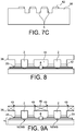
- cords along the cavities etched in the cover It may be a wide cord as shown in the figure 7C , or preferably several narrow cords parallel to each other as shown in the Figures 2A to 2C . In the latter case, for example the cords and the spaces between the cords can be from a few ⁇ m to a few tens of micrometers.
- the beads have a regular structure and a close sealing surface over the entire structure to be sealed so as to ensure a uniform crushing of the dry film with a reasonable pressure during the sealing step.
- the cover substrate 38 is then ready to be sealed on the substrate of the NEMS / MEMS 4 structure.
- the sealing is carried out on sealing equipment which makes it possible to control the temperature and the pressure applied between the cover and the substrate to be sealed.
- the substrate 4 and the cover substrate 38 are aligned by means of the marks made previously on the substrates.
- the pressure applied is of the order of a few kN to a few tens of kN, and for example the temperature is between 100 ° C. and 200 ° C.
- the substrate 4 and the cover substrate 38 are then assembled.
- the fluid channels are then sealed at the lateral edges of the channels.
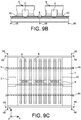
- the element thus obtained and represented on the figure 8 includes a plurality of fluid channel devices.
- an assembly such as that of the figure 8 is made from circular substrates used in microelectronics.
- the separation process firstly comprises a step intended to release the electrical contact pads.
- the contact pads of a device located on one side of the channel 6 are adjacent to those of the neighboring device located on one side of the channel of the neighboring device.
- the step of disengaging the studs is therefore intended to lead into the cavities 44 receiving the studs.
- This step is designated STR for Saw To Reveal in English.
- This step includes cutting the substrate of the cover locally in line with the contact pads so as to open into the cavities 44.
- the cutting lines 45 are symbolized by the broken lines, the cuts delimiting cut portions 46 which are removed.
- This cutting is carried out in the XZ planes, so the sawing residues do not penetrate into the channels.
- a step of precutting of each cover and of the substrate 4 is carried out in planes YZ in a direction perpendicular to the direction X of the fluid channels only so as to longitudinally separate the devices with fluid channels.
- cutting or precut lines are also produced in the substrate 4 in XZ planes parallel to the direction X of the fluid channels so as to transversely separate the devices with fluid channels.
- the fluid channel devices are separated using the precut patterns 48 and 49, for example cleavage, laser cutting.
- sawing is avoided with regard to the production of patterns 48 which would risk polluting the interior of the fluid channels.
- This separation technique is particularly advantageous since it makes it possible to reveal the electrical contact pads while eliminating, at the end of the manufacturing process, any functionalization layer present on the surface of these pads. In addition, it makes it possible to separate the chips from each other while preserving the integrity of the fluid channel.
- the substrate may not include a cavity 44 in the case where the substrate 38 is etched to the contact pads.
- cavities 44 are provided as on the figure 8 , the etching being stopped as soon as one emerges in the cavities, which makes it possible to reveal the contacts. Polishing of the cover substrate may have a bond until it leads to cavities previously formed above the contact pads, technique designated "grinding to reveal" in English. In this case, it is necessary to have cavities of type 44 deeper than the cavities of the fluid channels in order to open into the cavities 44 without opening into the fluid channels in order to preserve their integrity.
- the invention it is possible to produce a fluid channel device comprising one or more mechanical structures suspended in the channel and one or more lateral electrical connections with a guaranteed seal, thus avoiding the formation of TSV in the substrate and also d '' avoid the presence in the fluid channel of structures ensuring electrical contact between the mechanical structure located inside the channel and the outside of this channel, of the metal pillar type extending TSVs made in the cover or of the column type in Si or glass with an engraved cavity inside allowing wire-bonding on a stud of the mechanical structure isolated from the cavity, as is conventionally done with metallic or polymer sealing approaches.
- the invention makes it possible to easily produce networks of mechanical structures by allowing dense and complex electrical interconnection as close as possible to mechanical structures with possibly several levels of metal.
- the invention can also make it possible to encapsulate all the structures and layers present in the channel except the sensitive structures. Finally, it allows the implementation of functionalization during the process on suspended mechanical structures.
Description
La présente invention se rapporte à un dispositif comportant un canal fluidique muni d'au moins un système micro ou nanoélectronique et à un procédé de réalisation d'un tel dispositif.The present invention relates to a device comprising a fluid channel provided with at least one micro or nanoelectronic system and to a method for producing such a device.
Les notions de systèmes microélectroniques ou nanoélectronique intègrent les systèmes microélectromécaniques ou MEMS (microelectromechanical systems en anglais) et les systèmes nanoélectromécaniques ou NEMS (Nanoelectromechanical systems). Par soucis de simplification ils seront nommés dans le reste de la description MEMS et NEMS. Ces systèmes sont aujourd'hui couramment employés dans de nombreux produits. De nouvelles applications apparaissent notamment du fait du développement des NEMS qui offrent de nouveaux avantages grâce à la réduction des dimensions. En particulier, du fait de la grande sensibilité en masse de ce type de systèmes, ils sont d'un grand intérêt pour les capteurs chimiques ou biologiques.The concepts of microelectronic or nanoelectronic systems integrate microelectromechanical systems or MEMS (microelectromechanical systems in English) and nanoelectromechanical systems or NEMS (Nanoelectromechanical systems). For the sake of simplification, they will be named in the rest of the MEMS and NEMS description. These systems are currently widely used in many products. New applications appear in particular due to the development of NEMS which offer new advantages thanks to the reduction of dimensions. In particular, due to the high mass sensitivity of this type of system, they are of great interest for chemical or biological sensors.
Un NEMS ou un MEMS comporte une partie fixe et au moins une partie suspendue (pouvant être mobile) ou partie sensible par rapport à la partie fixeA NEMS or MEMS has a fixed part and at least one suspended part (which can be mobile) or sensitive part relative to the fixed part
Mais pour ces applications en particulier, il est nécessaire de gérer l'exposition de la structure de type MEMS ou NEMS, qui offre des caractéristiques physico-chimiques particulières, à un milieu environnant, en général gazeux ou liquide. Pour cela la structure sensible MEMS ou NEMS est disposée dans un canal fluidique dans lequel s'écoule le milieu et permet la mise en contact du milieu à analyser avec la structure sensible NEMS ou MEMS.But for these applications in particular, it is necessary to manage the exposure of the MEMS or NEMS type structure, which offers particular physicochemical characteristics, to a surrounding medium, generally gaseous or liquid. For this, the MEMS or NEMS sensitive structure is placed in a fluid channel in which the medium flows and allows the medium to be analyzed to be brought into contact with the NEMS or MEMS sensitive structure.
Ces structures sensibles sont reliées à un système électronique d'alimentation et de collecte de signaux par des liaisons électriques, celles-ci reliant la structure au système électronique situé à l'extérieur du canal fluidique.These sensitive structures are connected to an electronic power supply and signal collection system by electrical connections, these connecting the structure to the electronic system located outside the fluid channel.
Le canal fluidique est réalisé en rapportant un capot sur un substrat comportant la ou les structures sensibles. Le capot est scellé de manière étanche sur le substrat et comporte au moins deux ouvertures pour assurer la circulation dans le canal du fluide à analyser. Le capot est formé par une cavité réalisée dans un substrat de plusieurs µm à plusieurs centaines de µm de profondeur par exemple.The fluid channel is produced by attaching a cover to a substrate comprising the sensitive structure or structures. The cover is sealed on the substrate and has at least two openings to ensure the circulation in the channel of the fluid to be analyzed. The cover is formed by a cavity made in a substrate of several µm to several hundred µm deep for example.
Le document
Le scellement du capot peut être de type scellement polymère, scellement moléculaire, scellement anodique, scellement eutectique, frittage verre, etc. Se pose alors le problème de la réalisation des liaisons électriques entre la ou les structures sensibles se trouvant à l'intérieur du canal fluidique et l'extérieur du canal fluidique puisque le scellement, tout en permettant ces liaisons électriques, doit être étanche.The cover seal may be of the polymer seal, molecular seal, anode seal, eutectic seal, glass sintering, etc. type. The problem then arises of making the electrical connections between the sensitive structure or structures located inside the fluid channel and the exterior of the fluid channel since the sealing, while allowing these electrical connections, must be sealed.
Une technique consiste, après scellement du capot, à ouvrir de larges cavités dans l'épaisseur du capot uniquement au-dessus des zones de plots métallisés pour permettre une reprise de contact directe par wirebonding sur ces plots, chaque plot de contact étant entouré d'un cordon de scellement, par exemple en polymère, pour isoler cette partie de la cavité. Mais cette technique présente l'inconvénient d'introduire des motifs supplémentaires pour ces passages électriques à l'intérieur du canal fluidique ce qui n'est pas souhaitable car ils peuvent être à l'origine de perturbation de la circulation du fluide, de génération de volumes morts, etc. Par ailleurs, cette technique est mal adaptée dans le cas de structures sensibles de type NEMS ou MEMS car ces structures requièrent des plots de contact en matériau semi-conducteur ou en métal de petite taille pour réduire les capacités parasites et être en mesure d'extraire un signal électrique exploitable avec un bon rapport signal/bruit. Enfin cette technique n'est pas adaptée pour des composants formés de NEMS ou MEMS en réseaux, car ceux-ci sont interconnectés entre eux avec une densité importante, ce qui implique la mise en œuvre de plots de très petites tailles, et éventuellement à l'aide de plusieurs niveaux métalliques.One technique consists, after sealing the cover, of opening large cavities in the thickness of the cover only above the areas of metallized pads to allow direct contact recovery by wirebonding on these pads, each contact pad being surrounded by a sealing bead, for example made of polymer, to isolate this part of the cavity. However, this technique has the drawback of introducing additional patterns for these electrical passages inside the fluid channel, which is undesirable since they can cause disturbance of the circulation of the fluid, generation of dead volumes, etc. Furthermore, this technique is ill-suited in the case of sensitive structures of the NEMS or MEMS type because these structures require contact pads made of semiconductor material or small metal to reduce the parasitic capacitances and be able to extract an exploitable electrical signal with a good signal / noise ratio. Finally, this technique is not suitable for components formed of NEMS or MEMS in networks, because these are interconnected with one another with a high density, which implies the implementation very small studs, and possibly using several metal levels.
Une autre technique pour réaliser ces connexions électriques tout en assurant l'étanchéité consiste à réaliser des connexions de type Via, par exemple des TSV (Through Silicon Via en anglais) ou TGV (Through Glass Via en anglais). Le document «
Le document
C'est par conséquent un but de la présente invention d'offrir un dispositif comportant au moins un canal fluidique, comportant une ou plusieurs structures sensibles situées dans le canal fluidique, et des liaisons électriques entre la ou les structures sensibles situées dans le canal fluidique et l'extérieur du canal fluidique ne présentant pas les inconvénients cités ci-dessus.It is therefore an object of the present invention to provide a device comprising at least one fluid channel, comprising one or more sensitive structures located in the fluid channel, and electrical connections between the sensitive structure (s) located in the fluid channel and the exterior of the fluid channel does not have the drawbacks mentioned above.
C'est également un but d'offrir un procédé de réalisation d'une telle structure à canal fluidique.It is also an aim to offer a method for producing such a fluid channel structure.
Le but mentionné ci-dessus est atteint par une structure comportant un canal fluidique formé par un substrat comprenant au moins une structure sensible, au moins une connexion électrique entre la structure sensible et une zone extérieure au canal fluidique, ladite connexion électrique étant formée sur la surface du substrat portant la structure sensible, une couche intermédiaire recouvrant au moins en partie la connexion électrique, ladite couche intermédiaire présentant une face libre apte au scellement du capot, et un capot scellé de manière étanche sur la face libre plane de la couche intermédiaire.The above-mentioned object is achieved by a structure comprising a fluid channel formed by a substrate comprising at least one sensitive structure, at at least one electrical connection between the sensitive structure and an area outside the fluid channel, said electrical connection being formed on the surface of the substrate carrying the sensitive structure, an intermediate layer covering at least partially the electrical connection, said intermediate layer having a free face suitable for sealing the cover, and a cover sealed in a sealed manner on the flat free face of the intermediate layer.
Dans la présente demande, on entend par "face de la couche intermédiaire apte au scellement", une face présentant un état de surface permettant le scellement avec les faces de base du capot, par exemple un scellement par film sec, un scellement moléculaire, eutectique ou par thermocompression. La face apte au scellement peut présenter une certaine rugosité ou un certain relief qui permet néanmoins le scellement.In the present application, the term "face of the intermediate layer suitable for sealing" means a face having a surface state allowing sealing with the base faces of the cover, for example a dry film seal, a molecular seal, eutectic or by thermocompression. The face suitable for sealing may have a certain roughness or a certain relief which nevertheless allows sealing.
La mise en œuvre d'une couche intermédiaire permet la réalisation de lignes de connexion latérale tout en assurant une réalisation simplifiée du scellement étanche entre le capot et le substrat, puisque le scellement est réalisé sur la couche intermédiaire avantageusement plane. En outre la ou les connexions étant réalisées sur la surface du substrat et recouvertes par la couche intermédiaire, elles ne perturbent pas l'écoulement contrairement aux autres solutions mentionnées précédemment, par exemple des TSV réalisés dans le capot.The implementation of an intermediate layer allows the realization of lateral connection lines while ensuring a simplified realization of the sealing between the cover and the substrate, since the sealing is carried out on the advantageously flat intermediate layer. In addition, the connection or connections being made on the surface of the substrate and covered by the intermediate layer, they do not disturb the flow unlike the other solutions mentioned above, for example TSVs made in the cover.
En d'autres termes, le dispositif à canal fluidique comporte une couche assurant une encapsulation des lignes de connexion au moins dans la zone de scellement avec le capot, cette couche permet alors la libération de la structure NEMS/MEMS tout en conservant une surface permettant le scellement au dessus des lignes de connexion, cette surface étant suffisamment plane pour réaliser un scellement étanche du capot sur la structure NEMS/MEMS.In other words, the fluid channel device includes a layer ensuring encapsulation of the connection lines at least in the sealing zone with the cover, this layer then allows the release of the NEMS / MEMS structure while retaining a surface allowing the sealing above the connection lines, this surface being sufficiently flat to effect a tight sealing of the cover on the NEMS / MEMS structure.
L'invention permet donc de ne pas recourir à la réalisation de via à travers le capot et/ou à l'ouverture de larges cavités dans l'épaisseur du capot pour permettre une reprise de contact. Le procédé de réalisation est donc sensiblement simplifié.The invention therefore makes it possible not to resort to the production of via through the cover and / or to the opening of large cavities in the thickness of the cover to allow contact to be resumed. The production process is therefore considerably simplified.
De manière très avantageuse, cette couche intermédiaire peut être telle qu'elle encapsule les matériaux de la structure NEMS ou MEMS sauf la partie sensible qui, de par leur présence dans le canal fluidique, pourraient interagir avec le milieu en circulation dans le canal, i.e. elle isole les matériaux de la structure NEMS ou MEMS autres que la partie sensible de l'intérieur du canal fluidique. C'est le cas par exemple avec les métaux ou diélectriques qui sont mis en œuvre dans le canal fluidique si la structure mécanique est constituée d'un réseau dense de NEMS. Dans ce cas-là, la couche intermédiaire est uniquement ouverte au niveau des structures NEMS destinées à interagir avec le milieu environnant.Very advantageously, this intermediate layer can be such that it encapsulates the materials of the NEMS or MEMS structure except the sensitive part which, due to their presence in the fluid channel, could interact with the medium circulating in the channel, ie it isolates the materials of the NEMS or MEMS structure other than the sensitive part of the interior of the fluid channel. This is the case for example with metals or dielectrics which are used in the fluid channel if the mechanical structure consists of a dense network of NEMS. In this case, the intermediate layer is only open at the level of the NEMS structures intended to interact with the surrounding medium.
De manière également très avantageuse, la présence de la couche intermédiaire permet la libération des structures mécaniques avant le scellement du capot. Ceci est particulièrement avantageux car on peut envisager des couches de fonctionnalisation des structures mécaniques variées mises en œuvre autrement que par voie liquide. Ces couches de fonctionnalisation sont beaucoup plus compatibles avec des structures mécaniques libérées. Elles peuvent mises en œuvre, par exemple par des dépôts en phase vapeur ou encore par évaporation, par épitaxie ou tout autre de méthode de formation, voire de report de couches. Grâce à l'invention, il est possible de déposer une couche de fonctionnalisation sur la structure NEMS ou MEMS et ainsi de les fonctionnaliser avant de sceller le capot sur le substrat portant les structures mécaniques. Dans ce cas, la couche de fonctionnalisation peut recouvrir entièrement la partie suspendue des structures mécaniques, offrant alors une surface d'interaction augmentée entre l'environnement et la couche de fonctionnalisation.Also very advantageously, the presence of the intermediate layer allows the release of the mechanical structures before the sealing of the cover. This is particularly advantageous since it is possible to envisage layers of functionalization of the various mechanical structures implemented other than by the liquid route. These functionalization layers are much more compatible with released mechanical structures. They can be implemented, for example by vapor phase deposits or by evaporation, epitaxy or any other method of formation, or even of layer transfer. Thanks to the invention, it is possible to deposit a functionalization layer on the NEMS or MEMS structure and thus to functionalize them before sealing the cover on the substrate carrying the mechanical structures. In this case, the functionalization layer can completely cover the suspended part of the mechanical structures, thus offering an increased interaction surface between the environment and the functionalization layer.
De manière préférée un film sec de résine est utilisé pour sceller la partie NEMS comportant la couche intermédiaire et le capot.Preferably, a dry resin film is used to seal the NEMS part comprising the intermediate layer and the cover.
Par ailleurs, la structure selon l'invention et son procédé de réalisation permet une réalisation collective de puces munies d'un canal fluidique, les puces étant séparées par pré-sciage entre les canaux et prédécoupe transversale aux canaux.Furthermore, the structure according to the invention and its production method allows a collective production of chips provided with a fluid channel, the chips being separated by pre-sawing between the channels and precut transverse to the channels.
La présente invention a alors pour objet un dispositif comportant un substrat comprenant au moins une structure microélectronique et/ou nanoélectronique comportant au moins une partie sensible et un canal fluidique défini entre ledit substrat et un capot, ledit canal fluidique comportant deux parois latérales et une paroi supérieure raccordant les deux parois latérales et une paroi inférieure formée par ledit substrat et au moins deux ouvertures pour assurer une circulation dans ledit canal, ladite structure microélectronique et/ou nanoélectronique étant située à l'intérieur du canal fluidique, au moins une ligne de connexion électrique s'étendant entre ladite structure microélectronique et/ou nanoélectronique et l'extérieur du canal fluidique, ladite ligne de connexion étant réalisée sur le substrat et passant sous l'une des parois latérales, ledit dispositif comportant également une couche intermédiaire comportant une face en contact avec des faces de base desdites parois latérales, ladite face de la couche intermédiaire présentant une aptitude au scellement avec les faces de base, ladite ligne de connexion étant au moins en partie recouverte par ladite couche intermédiaire au moins à l'aplomb de la face de base de ladite paroi latérale, lesdites parois latérales étant solidarisées de manière étanche sur ledit substrat par scellement sur ladite couche intermédiaire.The present invention therefore relates to a device comprising a substrate comprising at least one microelectronic and / or nanoelectronic structure comprising at least one sensitive part and a fluid channel defined between said substrate and a cover, said fluid channel comprising two lateral walls and one wall. superior connecting the two side walls and a bottom wall formed by said substrate and at least two openings to ensure circulation in said channel, said microelectronic and / or nanoelectronic structure being located inside the fluid channel, at least one electrical connection line extending between said microelectronic and / or nanoelectronic structure and the exterior of the fluid channel, said connection line being formed on the substrate and passing under one of the side walls, said device also comprising an intermediate layer comprising a face in contact with base faces of said side walls, said face of the intermediate layer having a sealability with the base faces, said connection line being at least partially covered by said intermediate layer at least directly above the face of base of said side wall, said side walls being tightly secured to said s ubstrate by sealing on said intermediate layer.
Par exemple, le dispositif comportant au moins une paire de lignes de connexion s'étendant latéralement de part et d'autre de la structure microélectronique et/ou nanoélectronique et passant chacune sous une paroi latérale.For example, the device comprising at least one pair of connection lines extending laterally on either side of the microelectronic and / or nanoelectronic structure and each passing under a side wall.
Dans un mode de réalisation, la couche intermédiaire recouvre, dans le canal fluidique, toute la structure microélectronique et/ou nanoélectronique à l'exception de sa partie sensible.In one embodiment, the intermediate layer covers, in the fluid channel, the entire microelectronic and / or nanoelectronic structure with the exception of its sensitive part.
La couche intermédiaire peut comporter un matériau isolant électrique, tel qu'un oxyde de silicium, ou un nitrure de silicium.The intermediate layer may include an electrical insulating material, such as a silicon oxide, or a silicon nitride.
Dans un mode avantageux, le dispositif comporte une couche de fonctionnalisation encapsulant au moins une partie de la partie sensible de la structure microélectronique et/ou nanoélectronique. La couche de fonctionnalisation peut comporter un ou plusieurs matériaux choisis parmi les matériaux organiques, ou inorganiques, les polymères, les oxydes, les semiconducteurs. La ou les couches de fonctionnalisation peuvent être réalisées par dépôt chimique en phase vapeur, par évaporation, épitaxie, porosification par gravure, dépôt par spray, spotting (dépôt de gouttes), etc. Il est particulièrement intéressant d'utiliser comme couche de fonctionnalisation des matériaux poreux.In an advantageous embodiment, the device comprises a functionalization layer encapsulating at least part of the sensitive part of the microelectronic and / or nanoelectronic structure. The functionalization layer can comprise one or more materials chosen from organic or inorganic materials, polymers, oxides, semiconductors. The functionalization layer (s) may be produced by chemical vapor deposition, by evaporation, epitaxy, porosification by etching, spray deposition, spotting (deposition of drops), etc. It is particularly advantageous to use porous materials as a functionalization layer.
Le dispositif peut comporter des lignes de connexion et des plots de contact, lesdits plots de contact étant situés à l'extérieur du canal fluidique, lesdites lignes de connexions s'étendant entre la structure microélectronique et/ou nanoélectronique et les plots de contact.The device may include connection lines and contact pads, said contact pads being located outside the fluid channel, said connection lines extending between the microelectronic and / or nanoelectronic structure and the contact pads.
Dans un exemple de réalisation, les lignes de connexion comportent plusieurs niveaux de métallisation au moins à l'intérieur du canal.In an exemplary embodiment, the connection lines comprise several metallization levels at least inside the channel.
Le scellement peut être réalisé avantageusement au moyen d'un film sec de scellement interposé entre la couche intermédiaire et les faces de base des parois latérales du capot. Le film sec est de manière préférée une résine avec des bases epoxy, phenol, acrylic ou silicone par exemple.The sealing can advantageously be carried out by means of a dry sealing film interposed between the intermediate layer and the base faces of the side walls of the cover. The dry film is preferably a resin with epoxy, phenol, acrylic or silicone bases for example.
Le film sec de scellement peut être structuré en plusieurs cordons au niveau des interfaces entre la couche intermédiaire et les faces de base des parois latérales. Avantageusement, les cordons sont sensiblement parallèles au canal fluidique.The dry sealing film can be structured in several beads at the interfaces between the intermediate layer and the base faces of the side walls. Advantageously, the cords are substantially parallel to the fluid channel.
Le dispositif peut également comporter au moins une couche de matériau interposé entre la couche intermédiaire et les faces de base des parois latérales réalisant un scellement eutectique, par thermo-compression, par sérigraphie ou un scellement par frittage de verre.The device can also comprise at least one layer of material interposed between the intermediate layer and the base faces of the side walls performing a eutectic sealing, by thermo-compression, by screen printing or a sealing by sintering of glass.
Le scellement peut également être un scellement moléculaire, aucune interposition de matériau entre le capot et la couche intermédiaire n'est alors requise.The seal can also be a molecular seal, no interposition of material between the cover and the intermediate layer is then required.
Dans un exemple de réalisation, la couche intermédiaire comporte une première couche en matériau isolant électrique en contact avec la ligne de connexion et une deuxième couche (déposée sur la première couche, ladite deuxième couche étant en un matériau tel qu'il est peu ou pas sensible à une étape de libération de la structure microélectronique et/ou nanoélectronique. Avantageusement la première couche présente une face plane sur laquelle est déposée la deuxième couche. La deuxième couche est par exemple en Si, en nitrure de silicium, en métal (AISi, AlCu, ...) ou en oxyde d'Hafnium (HfO2)... Cette première couche est avantageusement planarisante.In an exemplary embodiment, the intermediate layer comprises a first layer of electrical insulating material in contact with the connection line and a second layer (deposited on the first layer, said second layer being of a material such that it is little or not sensitive to a step of releasing the microelectronic and / or nanoelectronic structure. Advantageously, the first layer has a flat face on which the second layer is deposited. The second layer is for example made of Si, silicon nitride, metal (AISi, AlCu, ...) or Hafnium oxide (HfO2) ... This first layer is advantageously planarizing.
Le canal forme dans une application très avantageuse une microcolonne de chromatographie en phase gazeuse.In a very advantageous application, the channel forms a gas chromatography microcolumn.
La présente invention a également pour objet un procédé de réalisation d'au moins un dispositif selon l'invention, comportant les étapes :
- a) réalisation de la structure microélectronique et/ou nanoélectronique sur un substrat et de la au moins une ligne de connexion,
- b) formation de la couche intermédiaire de sorte à ce qu'elle présente une face libre sensiblement plane présentant une ouverture au-dessus de ladite au moins partie sensible
- c) réalisation d'un substrat capot, comportant un canal fluidique,
- d) scellement du substrat capot sur la couche intermédiaire de sorte que le canal fluidique soit disposé en regard de la structure microélectronique et/ou nanoélectronique.
- a) making the microelectronic and / or nanoelectronic structure on a substrate and the at least one connection line,
- b) formation of the intermediate layer so that it has a substantially flat free face having an opening above said at least sensitive part
- c) production of a cover substrate, comprising a fluid channel,
- d) sealing of the cover substrate on the intermediate layer so that the fluid channel is disposed opposite the microelectronic and / or nanoelectronic structure.
Lors de l'étape b), la couche est selon un mode avantageux déposée puis structurée pour être éliminée au-dessus de tout ou partie des parties sensibles des structures MEMS/NEMS.During step b), the layer is, according to an advantageous mode, deposited and then structured to be eliminated above all or part of the sensitive parts of the MEMS / NEMS structures.
L'étape c) peut-être réalisée à n'importe quel moment du procédé à condition que cela soit avant l'étape d).Step c) can be carried out at any time during the process, provided that this is before step d).
Le procédé peut comporter, après l'étape b), une étape de libération de ladite structure microélectronique et/ou nanoélectronique.The method may include, after step b), a step of releasing said microelectronic and / or nanoelectronic structure.
Le procédé de réalisation peut également comporter une étape de réalisation d'une couche de fonctionnalisation à l'intérieur du canal fluidique sur la structure microélectronique et/ou nanoélectronique et/ou sur les parois du capot et/ou sur la couche intermédiaire, ladite étape étant effectuée avant le scellement.The production method may also include a step of producing a functionalization layer inside the fluid channel on the microelectronic and / or nanoelectronic structure and / or on the walls of the cover and / or on the intermediate layer, said step being performed before sealing.
En variante, la couche de fonctionnalisation peut être formée avant la libération de la partie sensible, voire avant la formation de la structure sensible.As a variant, the functionalization layer can be formed before the release of the sensitive part, or even before the formation of the sensitive structure.
Des couches de fonctionnalisation à différents emplacements du canal fluidique peuvent être déposées, dans ce cas, ces couches peuvent être de même nature ou non.Functionalization layers at different locations in the fluid channel can be deposited, in this case, these layers can be of the same nature or not.
Dans un exemple avantageux, l'étape de scellement utilise un film sec, cette étape peut comporter les sous-étapes :
- laminage du film sec sur les faces de base des parois du capot,
- structuration du film sec
- rapprochement du capot et du substrat comportant les structure microélectronique et/ou nanoélectronique,
- application d'une pression de sorte à écraser le film sec.
- laminating the dry film on the base faces of the cover walls,
- structuring of the dry film
- approximation of the cover and the substrate comprising the microelectronic and / or nanoelectronic structure,
- application of pressure so as to crush the dry film.
Un chauffage peut également être appliqué lors de l'application de la pression.Heating can also be applied when applying pressure.
Des préparations de surface peuvent être avantageusement appliquées sur les interfaces avant le scellement par film sec pour améliorer encore l'adhérence, la préparation peut être un traitement de type plasma.Surface preparations can advantageously be applied to the interfaces before sealing with dry film to further improve the adhesion, the preparation can be a plasma type treatment.
La réalisation de la couche intermédiaire peut avoir lieu par dépôt d'une première couche de matériau isolant électrique et de dépôt d'une deuxième couche sur la première couche.The intermediate layer can be produced by depositing a first layer of electrical insulating material and depositing a second layer on the first layer.
Le matériau de la deuxième couche est de préférence choisi peu ou pas sensible à l'étape de libération de la structure microélectronique et/ou nanoélectronique, lorsque ce procédé comporte une étape de libération.The material of the second layer is preferably chosen to have little or no sensitivity to the step of releasing the microelectronic and / or nanoelectronic structure, when this method includes a release step.
Selon un autre exemple de réalisation, le scellement est un scellement eutectique ou par thermo-compression, ou par scellement moléculaire ou par sérigraphie.According to another exemplary embodiment, the seal is a eutectic seal or by thermo-compression, or by molecular seal or by screen printing.
La libération peut être obtenue par gravure utilisant l'acide fluorhydrique vapeur.The release can be obtained by etching using hydrofluoric acid vapor.
Lorsque plusieurs dispositifs sont réalisés simultanément, ledit substrat peut comporter plusieurs structures microélectroniques et/ou nanoélectroniques et le substrat capot comportant plusieurs capots, les capots étant scellés simultanément sur le substrat comportant les structures microélectroniques et/ou nanoélectroniques, de sorte qu'un canal fluidique d'un dispositif puisse communiquer ou non avec le canal fluidique d'autres dispositifs.When several devices are produced simultaneously, said substrate can comprise several microelectronic and / or nanoelectronic structures and the cover substrate comprising several covers, the covers being sealed simultaneously on the substrate comprising the microelectronic and / or nanoelectronic structures, so that a fluid channel of a device may or may not communicate with the fluid channel of other devices.
Lorsque plusieurs dispositifs sont disposés en matrice, les canaux fluidiques de dispositifs en lignes peuvent communiquer entre eux alors que les canaux fluidiques de dispositifs en colonne sont disposés les uns à côtés des autres.When several devices are arranged in a matrix, the fluid channels of line devices can communicate with one another while the fluid channels of column devices are arranged one next to the other.
Lorsque plusieurs dispositifs sont réalisés, le procédé de réalisation peut comporter les étapes de :
- de réalisation de prédécoupes dans une direction perpendiculaire aux canaux fluidiques dans le substrat capot et dans le substrat portant les structures microélectroniques et/ou nanoélectroniques,
- de réalisation de découpes ou de prédécoupes dans une direction parallèle aux canaux fluidiques dans le substrat portant les structures microélectroniques et/ou nanoélectroniques,
- de séparation des dispositifs.
- making precuts in a direction perpendicular to the fluid channels in the cover substrate and in the substrate carrying the microelectronic and / or nanoelectronic structures,
- making cuts or precuts in a direction parallel to the fluid channels in the substrate carrying the microelectronic and / or nanoelectronic structures,
- separation of devices.
Ces découpes partielles ou totales peuvent être obtenues par sciage ou amorphisation laser.These partial or total cuts can be obtained by sawing or laser amorphization.
La séparation des dispositifs est réalisée par exemple par clivage.The separation of the devices is carried out for example by cleavage.
Le substrat capot peut comporter des cavités formées préalablement entre les canaux dans lesquelles se trouvent les plots de contact après scellement, le procédé peut comporter en outre une étape de découpage du substrat capot pour ouvrir lesdites cavités. Cette étape peut être réalisée avant ou après les découpes ou prédécoupes pour séparer les dispositifs.The cover substrate may include cavities formed beforehand between the channels in which the contact pads are located after sealing, the method may also include a step of cutting the cover substrate to open said cavities. This step can be carried out before or after the cuts or precuts to separate the devices.
Lorsqu'une couche de fonctionnalisation a été formée sur ladite structure microélectronique et/ou nanoélectronique et sur les plots de contact avant le scellement, ledit procédé peut comporter l'étape de retrait par gravure de la couche de fonctionnalisation sur les plots de contact après scellement et ouverture des cavités dans le capot, lesdits capots formant des masques à cette gravure pour les structures microélectroniques et/ou nanoélectroniques.When a functionalization layer has been formed on said microelectronic and / or nanoelectronic structure and on the contact pads before sealing, said method may include the step of removing by etching the functionalization layer on the contact pads after sealing and opening the cavities in the cover, said covers forming masks in this etching for microelectronic and / or nanoelectronic structures.
La présente invention sera mieux comprise à l'aide de la description qui va suivre et des dessins en annexes sur lesquels :
- la
figure 1A est une vue de dessus d'un dispositif de canal fluidique intégrant des structures MEMS/NEMS avec une couche intermédiaire selon un premier mode de réalisation, - la
figure 1B est une vue agrandie de lafigure 1A , - les
figures 2A, 2B ,2B', 2C ,2C' sont des vues en coupe de lafigure 1B suivant le plan A-A de différents exemples de réalisation dans lequel le scellement est réalisé au moyen d'un film sec, - la
figure 3A est une vue de dessus d'un dispositif à canal fluidique selon un autre mode de réalisation dans lequel la couche intermédiaire recouvre en partie la structure MEMS/NEMS à l'intérieur du canal, délimitant un canal parallèle au canal fluidique, - la
figure 3B est une vue de dessus d'un dispositif à canal fluidique dans lequel la couche intermédiaire recouvre en partie la structure MEMS/NEMS à l'intérieur du canal, délimitant une fenêtre au niveau de la partie sensible, - la
figure 3C est une vue en coupe de lafigure 3A ou de lafigure 3B suivant le plan B-B, - la
figure 4A est une vue de dessus d'une variante du dispositif de lafigure 3A , - la
figure 4B est une vue en coupe de lafigure 4A suivant le plan C-C, - les
figures 5A à 5C sont des vues en coupe transversale d'un dispositif à canal fluidique selon le premier mode de réalisation, présentant d'autres types de scellement et avec ou sans une couche de fonctionnalisation sur la partie MEMS/NEMS, - les
figures 6A à 6L sont des vues schématiques d'un procédé de réalisation du substrat muni d'au moins une structure MEMS ou NEMS pour la réalisation d'un dispositif à canal fluidique selon l'invention, - les
figures 7A à 7C sont des vues schématiques d'un procédé de réalisation d'un capot pour la réalisation d'un dispositif à canal fluidique selon l'invention, - la
figure 8 est une représentation schématique de l'étape d'assemblage du capot de lafigure 7C et du substrat de lafigure 6K , - les
figures 9A à 9C sont des représentations schématiques de différentes étapes destinées à la séparation des dispositifs à canaux fluidiques dans le cas d'un procédé de réalisation collective des dispositifs.
- the
figure 1A is a top view of a fluid channel device integrating MEMS / NEMS structures with an intermediate layer according to a first embodiment, - the
figure 1B is an enlarged view of thefigure 1A , - the
Figures 2A, 2B ,2B ', 2C ,2C ' are sectional views of thefigure 1B according to the plane AA of various exemplary embodiments in which the sealing is carried out by means of a dry film, - the
figure 3A is a top view of a fluid channel device according to another embodiment in which the intermediate layer partially covers the MEMS / NEMS structure inside the channel, delimiting a channel parallel to the fluid channel, - the
figure 3B is a top view of a fluid channel device in which the intermediate layer partially covers the MEMS / NEMS structure inside the channel, delimiting a window at the level of the sensitive part, - the
figure 3C is a sectional view of thefigure 3A or fromfigure 3B according to plan BB, - the
figure 4A is a top view of a variant of the device of thefigure 3A , - the
figure 4B is a sectional view of thefigure 4A according to the CC plan, - the
Figures 5A to 5C are views in cross section of a fluid channel device according to the first embodiment, having other types of sealing and with or without a functionalization layer on the MEMS / NEMS part, - the
Figures 6A to 6L are schematic views of a method for producing the substrate provided with at least one MEMS or NEMS structure for the production of a fluid channel device according to the invention, - the
Figures 7A to 7C are schematic views of a method for producing a cover for the production of a fluid channel device according to the invention, - the
figure 8 is a schematic representation of the assembly step of the hood of thefigure 7C and the substrate of thefigure 6K , - the
Figures 9A to 9C are schematic representations of different stages intended for the separation of devices with fluid channels in the case of a process for the collective production of the devices.
Dans la présente demande, on entend par partie NEMS/MEMS une structure mécanique comportant une structure fixe et au moins une structure sensible et des moyens d'actionnement et/ou de transduction d'au moins une caractéristique de la structure sensible.In the present application, the term NEMS / MEMS is understood to mean a mechanical structure comprising a fixed structure and at least one sensitive structure and means for actuating and / or transducing at least one characteristic of the sensitive structure.
La structure sensible peut être une structure mécanique suspendue et comporter des moyens d'actionnement et/ou de transduction du mouvement mécanique. Des connexions électriques sont prévues pour relier la structure mécanique au milieu extérieur. Cette partie MEMS/NEMS peut comporter un réseau de structures NEMS et/ou MEMS, avec éventuellement plusieurs niveaux de métallisation pour réaliser les interconnexions requises. A des fins de simplicité, un MEMS ou un NEMS sera désigné par NEMS.The sensitive structure can be a suspended mechanical structure and include means for actuating and / or transducing the mechanical movement. Electrical connections are provided to connect the mechanical structure to the outside environment. This MEMS / NEMS part can include a network of NEMS and / or MEMS structures, possibly with several metallization levels to achieve the required interconnections. For simplicity, a MEMS or NEMS will be designated by NEMS.
Les expressions "partie sensible" et "partie suspendue" seront utilisées indifféremment sachant que dans certaines applications de type électromécanique cette partie sensible est mobile.The expressions “sensitive part” and “suspended part” will be used interchangeably knowing that in certain applications of electromechanical type this sensitive part is mobile.
Les mêmes références seront utilisées pour désigner les éléments ayant les mêmes fonctions et sensiblement la même forme.The same references will be used to designate the elements having the same functions and substantially the same shape.
Sur les
Le dispositif comporte un canal fluidique 2, qui est rectiligne d'axe X dans l'exemple représenté. Le canal fluidique 2 est délimité par un substrat 4 et un capot 6 reporté sur le substrat 4. Par exemple, l'écoulement dans le canal fluidique se fait d'une extrémité longitudinale 2.1 à l'autre 2.2 du canal fluidique 2.The device comprises a
Dans l'exemple représenté, le capot 6 est formé à partir d'un substrat dans lequel une cavité 5 a été ménagée. La cavité 5 délimite avec le substrat portant la structure NEMS/MEMS le canal fluidique 2 qui assure la circulation et la distribution d'un mélange gazeux ou liquide. Le canal est délimité par deux parois latérales 6.1, un fond supérieur 6.2 reliant les deux parois latérales 6.1 et un fond inférieur formé par le substrat 4. Les parois latérales 6.1 présentent des faces de base qui permettent le scellement du capot sur le substrat.In the example shown, the
Il sera compris que l'extrémité d'entrée et/ou l'extrémité de sortie du canal fluidique pourraient être par exemple réalisées dans le fond supérieur 6.2 du canal ou encore dans le substrat 4.It will be understood that the inlet end and / or the outlet end of the fluid channel could for example be made in the upper bottom 6.2 of the channel or also in the
Alternativement, le capot 6 pourrait présenter une forme plus complexe, par exemple celui-ci pourrait comporter un long canal de forme optimisée, par exemple en spirale, permettant de réaliser une colonne de chromatographie assurant la fonction de séparation des composés d'un mélange, la colonne intégrant une structure NEMS/MEMS.Alternatively, the
Le substrat comporte une structure NEMS/MEMS 7 situé à l'intérieur du canal fluidique 2. Dans l'exemple représenté, la structure NEMS/MEMS comporte trois NEMS alignés le long de l'axe longitudinal X.The substrate comprises a NEMS /
Le dispositif comporte également des lignes de connexion électrique 8 s'étendant latéralement entre les NEMS situés dans le canal fluidique 2 et des plots 9 situés à l'extérieur du canal fluidique. Les plots 9 sont par exemple réalisés directement dans le matériau semi-conducteur de la structure NEMS\MEMS. Ils peuvent avantageusement être recouverts de métal pour assurer un bon contact électrique. Les lignes de connexion 8 peuvent être en semi-conducteur dopé du type de celui formant la structure NEMS/MEMS.The device also includes
Les lignes de connexion 8 sont séparées par des tranchées 11 de sorte à isoler électriquement les lignes de connexion 8 entre elles.The connection lines 8 are separated by
Ces lignes de connexion 8 peuvent être réalisées avec un ou plusieurs niveaux de métal séparés par un matériau diélectrique comme cela sera décrit pas la suite.These
Ces lignes peuvent également être réalisées en semi-conducteur recouvert de métal afin de réduite la résistance électrique de la ligne.These lines can also be made of semiconductor covered with metal in order to reduce the electrical resistance of the line.
En variante, les lignes de connexion peuvent être en métal, le contact entre le semi-conducteur dans lequel est réalisée la structure et le métal étant alors localisé soit dans le canal fluidique, soit à l'extérieur de ce canal, soit éventuellement sous la zone de scellement séparant le canal fluidique de l'extérieur. De manière avantageuse, les lignes de connexion 8 comportent une partie réduite en matériau semi-conducteur seul pour limiter les résistances électriques et les capacités parasites qui peuvent dégrader les performances des composants NEMS.As a variant, the connection lines can be made of metal, the contact between the semiconductor in which the structure is made and the metal then being located either in the fluid channel, or outside this channel, or possibly under the sealing zone separating the fluid channel from the outside. Advantageously, the
De préférence, les pistes métalliques pour former les lignes de connexion sont réalisées de façon préférentielle en configuration damascène pour éviter la formation d'interstices ou voids ou de zones de plus faible densité dans le diélectrique de remplissage et dans le matériau de la couche intermédiaire, ce qui est susceptible de conduire à des infiltrations et gravures indésirables lors de l'étape de libération des structures mécaniques, y compris latéralement sous les zones de scellement entre le substrat et le capot. En outre, ils pourraient conduire à des fuites latérales hors du canal fluidique.Preferably, the metal tracks for forming the connection lines are preferably produced in a damascene configuration to avoid the formation of interstices or voids or zones of lower density in the filling dielectric and in the material of the intermediate layer, which is likely to lead to undesirable infiltration and etching during the step of releasing the mechanical structures, including laterally under the sealing zones between the substrate and the cover. In addition, they could lead to lateral leaks out of the fluid channel.
Dans l'exemple représenté, trois paires de lignes de connexion électriques 8 s'étendant latéralement de part et d'autre du canal fluidique 2 sont prévues par NEMS.In the example shown, three pairs of
Un dispositif comportant au moins deux lignes de connexion latérales s'étendant du même côté par rapport à l'axe X ne sort pas du cadre de la présente invention.A device comprising at least two lateral connection lines extending on the same side with respect to the axis X is not beyond the scope of the present invention.
Sur la
Dans l'exemple représenté, la structure suspendue du NEMS est formée par une poutre 10 encastrée à l'une de ses extrémités longitudinales, par exemple deux jauges 12, par exemple piézorésistives, servent à détecter le déplacement de la poutre 10. On peut voir les extrémités des lignes de connexion 8 connectées à la structure NEMS/MEMS.In the example shown, the suspended structure of the NEMS is formed by a
Sur la
Le substrat 4 comporte un empilement d'une couche sacrificielle 14 utilisée pour la réalisation du NEMS, d'une couche 16 en semi-conducteur dans laquelle sont réalisées la partie fixe et la partie mobile du NEMS.The
Dans cet exemple, les lignes de connexion 8 sont formées à la fois dans la couche 16 et d'une ligne en métal 18 recouvrant la couche 16.In this example, the
Une couche intermédiaire 20 recouvre au moins partiellement les lignes de connexion 8 et une couche de scellement 22 est disposée entre la couche intermédiaire 20 et le capot 6.An
La couche intermédiaire 20 est présente au moins au niveau de l'interface de scellement entre la structure NEMS/MEMS 7 et le capot et est absente des zones de la structure NEMS/MEMS afin de laisser la ou les parties partie de la structure NEMS/MEMS suspendue en contact avec le milieu présent dans le canal fluidique. Dans le premier mode de réalisation représenté sur les
La couche intermédiaire 20 comporte une première face 20.1 en contact avec les lignes de connexion 8, cette face 20.1 suivant la topologie des lignes de connexion 8 et du substrat 4 et une deuxième face 20.2 en contact avec le capot 6. La couche intermédiaire 20 est telle que la deuxième face 20.2 soit apte à réaliser le scellement du capot 6 comportant la partie NEMS, en assurant à la fois l'étanchéité le long du canal fluidique et le passage des lignes de connexion 8 et ceci de manière simplifiée. La présence de la couche intermédiaire 20 permet de compenser la topologie générée par la formation préalable de la structure NEMS/MEMS et des lignes de connexion 8.The
Comme indiqué ci-dessus, la couche intermédiaire 20 permet le passage d'au moins une partie des interconnexions électriques entre l'intérieur du canal fluidique 2 et l'extérieur du canal fluidique 2 tout en assurant une interface de scellement relativement plane facilitant l'obtention d'une étanchéité.As indicated above, the
Dans l'exemple représenté, la couche intermédiaire 20 présente des propriétés d'isolation électrique de sorte à isoler électriquement les lignes de connexion 8 entre elles. En outre, son matériau est choisi de sorte à permettre l'obtention d'une face 20.2 suffisamment plane pour le scellement. En fonction du type de scellement, l'état de surface de la face 20.2 obtenu directement après le dépôt de la couche intermédiaire peut être suffisant, ou une étape de planarisation est réalisée par exemple une étape de polissage mécano-chimique après la formation de la couche intermédiaire.In the example shown, the
Le matériau de la couche intermédiaire est choisi apte à être gravé, par exemple en gravure anisotrope.The material of the intermediate layer is chosen able to be etched, for example in anisotropic etching.
De préférence, le matériau de la couche intermédiaire 20 est choisi de sorte à présenter une bonne sélectivité à la gravure par rapport au procédé de libération des structures mécaniques et à ne pas générer de résidu lors de cette étape.Preferably, the material of the
Le matériau de la couche intermédiaire est également choisi de sorte à être compatible avec les matériaux utilisés pour l'assemblage final du dispositif entre le substrat portant la structure NEMS/MEMS et le capot.The material of the intermediate layer is also chosen so as to be compatible with the materials used for the final assembly of the device between the substrate carrying the NEMS / MEMS structure and the cover.
Dans le cas où une couche de fonctionnalisation est mise en œuvre, le matériau de la couche intermédiaire est choisi compatible avec celui de la couche de fonctionnalisation, en particulier de sorte à assurer une bonne adhérence de cette dernière.In the case where a functionalization layer is used, the material of the intermediate layer is chosen to be compatible with that of the functionalization layer, in particular so as to ensure good adhesion of the latter.
Par exemple, le matériau de la couche intermédiaire est un matériau diélectrique, par exemple un oxyde de silicium, comme par exemple le du SiO2 ou un oxyde formé à base de silane ou un oxyde formé à base de tetraethylorthosilicate (TEOS), un oxyde de silicium de type LTO (Low Temperature Oxyde) formé par dépôt chimique en phase vapeur basse pression ou LPCVD (Low Pressure Chemical Vapor Déposition) non dopé ou bien dopé au phosphore (PSG : phospho-Silicate-Glass) ou encore dopé au Bore et Phosphore (BPSG : Boro-Phospho-Silicate Glass), un oxyde déposé par dépôt chimique en phase vapeur assisté par plasma ou PECVD (Plasma Enhanced Chemical Vapor Déposition).For example, the material of the intermediate layer is a dielectric material, for example a silicon oxide, such as for example SiO 2 or an oxide formed from silane or an oxide formed from tetraethylorthosilicate (TEOS), an oxide LTO type silicon (Low Temperature Oxide) formed by low pressure chemical vapor deposition or LPCVD (Low Pressure Chemical Vapor Deposition) undoped or doped with phosphorus (PSG: phospho-Silicate-Glass) or doped with Boron and Phosphorus (BPSG: Boro-Phospho-Silicate Glass), an oxide deposited by chemical vapor deposition assisted by plasma or PECVD (Plasma Enhanced Chemical Vapor Deposition).
De manière très avantageuse, la couche intermédiaire 20 comporte plusieurs matériaux présentant chacun des propriétés intervenant dans la réalisation du dispositif. Par exemple, ces matériaux peuvent être disposés en couches successives. Par exemple, la couche intermédiaire comporte deux couches, une première couche déposée sur les lignes de connexion, désignée couche planarisante, qui permet de combler la topologie de la structure NEMS/MEMS et des lignes de connexion tout en assurant l'isolation électrique, et une deuxième couche déposée sur la première couche destinée à accroître la protection de l'ensemble lors de l'étape de libération de la structure mécanique.Very advantageously, the
La planéité de la couche planarisante assure la planéité de la couche de protection. Ainsi, une plus grande liberté est permise au niveau du choix du matériau pour la couche planarisante. A titre d'exemple, le matériau de la première couche est en oxyde de silicium et le matériau de la deuxième couche est en silicium amorphe ou en tout autre matériau capable de tenir la libération par l'acide fluorhydrique dans le cas ou le couche sacrificielle est en oxyde de silicium, comme un métal, un nitrure de silicium, etc. qui permet de protéger la surface supérieure de la première couche en oxyde lors de la libération.The flatness of the planarizing layer ensures the flatness of the protective layer. Thus, greater freedom is allowed in the choice of material for the planarizing layer. For example, the material of the first layer is made of silicon oxide and the material of the second layer is made of amorphous silicon or any other material capable of holding the release by hydrofluoric acid in the case where the sacrificial layer is made of silicon oxide, such as a metal, silicon nitride, etc. which protects the upper surface of the first oxide layer upon release.
Cette réalisation en au moins une couche planarisante et une couche de protection est particulièrement intéressante, car les vitesses de gravure des oxydes de silicium formant la couche planarisante sont en général très supérieures, par exemple au moins 10 fois supérieure, à la vitesse de gravure de la couche d'oxyde d'un substrat SOI par exemple qui est effectuée lors de la libération de la ou des structures mobiles. En l'absence d'une telle couche de protection, la gravure de libération de la ou les structures mobiles pourrait occasionner une consommation importante de la couche planarisante. Cette réalisation en deux couches permet donc avantageusement de réduire l'épaisseur de la couche planarisante. Par exemple, son épaisseur peut être de quelques dizaines de nm.This embodiment in at least one planarizing layer and a protective layer is particularly advantageous, since the etching speeds of the silicon oxides forming the planarizing layer are generally much higher, for example at least 10 times higher, than the etching speed of the oxide layer of an SOI substrate, for example, which is carried out when the mobile structure (s) are released. In the absence of such a protective layer, the release etching of the mobile structure or structures could cause significant consumption of the planarizing layer. This embodiment in two layers therefore advantageously makes it possible to reduce the thickness of the planarizing layer. For example, its thickness can be a few tens of nm.
Dans la réalisation où la couche intermédiaire ne comporte qu'un seul matériau son épaisseur est déterminée pour tenir compte de la consommation de matériau lors de la gravure de libération. Dans ce cas, l'épaisseur de la couche intermédiaire est par exemple de l'ordre de quelques µm.In the embodiment where the intermediate layer comprises only one material, its thickness is determined to take account of the consumption of material during the release etching. In this case, the thickness of the intermediate layer is for example of the order of a few μm.
Dans l'exemple des
Par exemple, un film mince de résine 22 est appliqué par laminage sur la face inférieure du capot 6 destinée à venir en contact de la couche intermédiaire 20 et est structuré par photolithographie. L'ensemble capot et film de résine, est reporté et scellé sur la couche intermédiaire 20.For example, a thin film of
Dans l'exemple représenté sur les
Le film sec est par exemple une résine avec des bases epoxy, phenol, acrylic ou silicone par exemple.The dry film is for example a resin with epoxy, phenol, acrylic or silicone bases for example.
Le film sec a par exemple une épaisseur comprise entre quelques µm à plusieurs dizaines de µm, voire quelques centaines de µm avec un multicouche de film sec, avantageusement quelques µm seulement pour éviter l'interaction entre le matériau de ce cordon de scellement avec le milieu se propageant dans le canal fluidique.The dry film has for example a thickness of between a few μm to several tens of μm, or even a few hundred μm with a multilayer of dry film, advantageously only a few μm to avoid interaction between the material of this sealing bead with the medium. propagating in the fluid channel.
Le scellement au moyen d'un film sec présente les avantages suivants :
- ce scellement peut avoir lieu à une température relativement basse, généralement en dessous de 250°C voire à température ambiante, ce qui est compatible avec l'existence de pistes métalliques. En effet, dans le cas de pistes en aluminium, la température maximale est d'environ 400°C.
- ce scellement est compatible avec un grand nombre de matériaux,
- le film sec peut être réalisé sur le capot malgré la forte topologie due au canal fluidique déjà formé, ce qui permet de ne pas effectuer des opérations de type photolithographie sur la structure NEMS/MEMS car celle-ci contient déjà des structures mécaniques libérées,
- ce scellement par film sec présente l'avantage d'être moins exigeant en termes d'état de surface nécessaire (planéité, rugosité, présence de particules) à l'interface de scellement que des scellements de type moléculaire ou eutectique ou même par thermo-compression. Ainsi la mise en œuvre d'un film sec peut permettre le scellement sans effectuer de polissage mécano-chimique préalable de la face plane 20.2 de la couche intermédiaire, son état de surface directement après dépôt pouvant être suffisant.
- this sealing can take place at a relatively low temperature, generally below 250 ° C. or even at ambient temperature, which is compatible with the existence of metal tracks. In fact, in the case of aluminum tracks, the maximum temperature is around 400 ° C.
- this sealing is compatible with a large number of materials,
- the dry film can be produced on the cover despite the strong topology due to the fluid channel already formed, which makes it possible not to carry out operations of the photolithography type on the NEMS / MEMS structure because it already contains released mechanical structures,
- this dry film sealing has the advantage of being less demanding in terms of surface condition required (flatness, roughness, presence of particles) at the sealing interface than molecular or eutectic type seals or even by thermosetting. compression. Thus, the implementation of a dry film can allow sealing without carrying out prior mechanical-chemical polishing of the flat face 20.2 of the intermediate layer, its surface condition directly after deposition may be sufficient.
Cette caractéristique permet avantageusement de réaliser ce scellement en présence d'une couche de fonctionnalisation à l'interface de scellement NEMS/Capot comme cela est représenté sur la
- Ce type de film offre en outre la possibilité de travailler avec des épaisseurs importantes, par exemple de l'ordre de plusieurs centaines de µm mais également des épaisseurs de quelques 10µm; voire quelques µm.
- De plus, ce type de film présente une bonne stabilité thermique.
- This type of film also offers the possibility of working with significant thicknesses, for example of the order of several hundreds of μm but also thicknesses of some 10 μm; even a few µm.
- In addition, this type of film has good thermal stability.
Un scellement par une autre technique ne sort pas du cadre de la présente invention, par exemple il pourrait s'agir d'un scellement moléculaire, d'un scellement eutectique, d'un scellement par thermo-compression, ou d'un scellement par sérigraphie.... Néanmoins, la mise en œuvre de ces techniques pourra se révéler plus complexe que le scellement par film sec. En effet, il sera préférable de limiter les températures mise en œuvre pour ne pas détériorer les pistes métalliques déjà présentes et éventuellement la couche de fonctionnalisation. Par ailleurs, ces températures seront choisies inférieures à environ 400°C pour au moins préserver les couches métalliques des lignes de connexion. Elles seront encore inférieures pour préserver certaines couches de fonctionnalisation par exemple de type polymère.A seal by another technique does not depart from the scope of the present invention, for example it could be a molecular seal, a eutectic seal, a heat-compression seal, or a seal by serigraphy .... However, the implementation of these techniques may prove to be more complex than sealing with a dry film. In fact, it will be preferable to limit the temperatures used so as not to deteriorate the metal tracks already present and possibly the functionalization layer. Furthermore, these temperatures will be chosen to be less than approximately 400 ° C. to at least preserve the metallic layers of the connection lines. They will be even lower to preserve certain functionalization layers, for example of the polymer type.
Dans le cas où le dépôt d'une couche est requis pour le scellement, celle-ci pouvant être éventuellement structurée sur une seule des deux parties, ce qui est le cas pour un scellement eutectique, ce dépôt et cette éventuelle structuration sont effectués de préférence sur le capot. Par exemple pour un eutectique Au-Si, une couche d'Au est déposée de préférence sur le capot.In the case where the deposition of a layer is required for sealing, the latter possibly being structured on only one of the two parts, which is the case for eutectic sealing, this deposition and this possible structuring are preferably carried out on the hood. For example, for an Au-Si eutectic, a layer of Au is preferably deposited on the cover.
Dans le cas où le dépôt d'une couche sur chacune des deux parties est requis, par exemple pour un scellement par thermo-compression, le dépôt sur la structure NEMS/MEMS est effectué avant la libération de la structure. Le matériau de cette couche est alors choisi compatible avec le procédé de libération de la structure NEMS/MEMS de sorte qu'elle ne se grave pas lors de cette étape technologique qui intervient juste avant le scellement. On utilisera alors par exemple une couche d'Au sur le capot et sur la couche intermédiaire pour un scellement Au-Au, dans le cas d'une libération des NEMS avec l'acide fluorhydrique en phase vapeur.In the case where the deposition of a layer on each of the two parts is required, for example for a thermo-compression sealing, the deposition on the NEMS / MEMS structure is carried out before the release of the structure. The material of this layer is then chosen to be compatible with the process of releasing the NEMS / MEMS structure so that it is not etched during this technological step which takes place just before sealing. A layer of Au will then be used for example on the cover and on the intermediate layer for an Au-Au sealing, in the case of release of the NEMS with hydrofluoric acid in the vapor phase.
Sur la
On entend par "couche de fonctionnalisation" une couche présente à la surface de la structure mécanique pour lui offrir des propriétés particulières. Par exemple dans le cas d'un capteur de gaz, la couche de fonctionnalisation permet d'accroître l'adsorption d'espèces gazeuses de manière éventuellement sélective ou, dans le cas d'un capteur biologique, la couche de fonctionnalisation permet d'assurer le greffage d'espèces biologiques. La couche de fonctionnalisation 24 est par exemple formée d'un ou des plusieurs matériaux organiques ou inorganiques, de polymères, d'oxydes, de composés carbonés, de semi-conducteurs ou autres matériaux poreux...The term “functionalization layer” is understood to mean a layer present on the surface of the mechanical structure to provide it with specific properties. For example in the case of a gas sensor, the functionalization layer makes it possible to increase the adsorption of gaseous species in a possibly selective manner or, in the case of a biological sensor, the functionalization layer makes it possible to ensure the grafting of biological species. The
L'invention permet très avantageusement de réaliser l'étape de dépôt de la couche de fonctionnalisation sur une structure mécanique déjà libérée, ce qui permet d'encapsuler presque totalement la structure mécanique avec la couche de fonctionnalisation (
De préférence, le scellement est réalisé au moyen d'un film sec 22 comme décrit ci-dessus, en effet la température d'un tel scellement est compatible avec la présence d'une couche de fonctionnalisation déposée ou formée elle-même à basse température, par exemple en polymère, etc.Preferably, the sealing is carried out by means of a
Comme cela a été décrit ci-dessus, le scellement par film sec présente l'avantage d'être moins exigeant en termes d'état de surface nécessaire (planéité, rugosité, présence de particules) à l'interface de scellement que des scellements de type moléculaire ou eutectique ou même par thermo-compression. Ainsi il permet un scellement même en présence d'une couche de fonctionnalisation à l'interface de scellement entre la couche intermédiaire et le capot.As described above, dry film sealing has the advantage of being less demanding in terms of the necessary surface condition (flatness, roughness, presence of particles) at the sealing interface than molecular or eutectic type seals or even by thermo-compression. Thus it allows sealing even in the presence of a functionalization layer at the sealing interface between the intermediate layer and the cover.
En outre, ce scellement étant compatible avec un grand nombre de matériaux, une grande liberté est offerte pour le choix de la ou des couches de fonctionnalisation qui peuvent être mises en œuvre. On peut alors envisager de mettre en œuvre des couches de fonctionnalisation de natures et/ou d'épaisseurs différentes sur les parties NEMS et Capot. Ceci est particulièrement intéressant dans le cas où le capot forme une colonne de chromatographie gazeuse. Dans ce cas le capot pourra recevoir une fonctionnalisation apte à remplir la fonction de séparation des analytes du mélange à analyser alors que le NEMS pourra recevoir une autre fonctionnalisation apte à optimiser ses performances en détection.In addition, this sealing being compatible with a large number of materials, great freedom is offered for the choice of the functionalization layer or layers which can be implemented. We can then consider implementing functionalization layers of different natures and / or thicknesses on the NEMS and Hood parts. This is particularly advantageous in the case where the cover forms a gas chromatography column. In this case, the cover can receive a functionalization capable of fulfilling the function of separating the analytes from the mixture to be analyzed, while the NEMS can receive another functionalization capable of optimizing its performance in detection.
Sur la
Sur les
Dans le cas d'un scellement moléculaire ou d'un scellement anodique, par exemple dans le cas où le capot est en verre, l'interface de scellement 26 est formée par la face du capot et la face du substrat à sceller.In the case of a molecular seal or an anodic seal, for example in the case where the cover is made of glass, the sealing
Aucun ajout de matériau n'est requis. Les faces à venir en contact sont préparés de manière connue par l'homme du métier, par exemple par polissage mécano-chimique (ou CMP (chemical-mechanical polishing) en anglais), i.e. la face 20.2 de la couche intermédiaire et la face inférieure du capot 6.No addition of material is required. The faces to come into contact are prepared in a manner known to those skilled in the art, for example by chemical mechanical polishing (or CMP (chemical-mechanical polishing) in English), ie the face 20.2 of the intermediate layer and the underside of the
Un scellement moléculaire en présence d'une couche de fonctionnalisation au niveau de l'interface, la couche de fonctionnalisation étant déposée après libération, est également envisageable.A molecular seal in the presence of a functionalization layer at the interface, the functionalization layer being deposited after release, is also conceivable.
Dans d'autres modes de scellement, l'interface de scellement est formée d'une couche en un ou plusieurs matériaux, il peut s'agir d'une couche en Au-Si, AIGe ou AuGe... par exemple dans le cas d'un scellement eutectique, de Au-Au, AuSn... par exemple dans le cas d'un scellement par thermo-compression ou de colles dans le cas d'un scellement par sérigraphie.In other sealing modes, the sealing interface is formed of a layer of one or more materials, it may be a layer of Au-Si, AIGe or AuGe ... for example in the case of an eutectic sealing, of Au-Au, AuSn ... for example in the case of a sealing by thermo-compression or of adhesives in the case of a sealing by screen printing.
Sur la
Sur la
Sur la
Sur les
Un dispositif à canal fluidique dans lequel la couche intermédiaire ne recouvrirait pas entièrement la partie de la structure NEMS/MEMS non destinée à venir en contact avec le milieu environnant ne sort pas du cadre de la présente invention.A fluid channel device in which the intermediate layer would not entirely cover the part of the NEMS / MEMS structure not intended to come into contact with the surrounding medium does not depart from the scope of the present invention.
Sur la
Cette encapsulation par la couche intermédiaire est particulièrement intéressante à mettre en œuvre dans le cas de réseaux de NEMS qui sont connectés entre eux par des pistes conductrices en semi-conducteur ou en métal avec éventuellement plusieurs niveaux d'interconnexions, l'isolation électrique entre les niveaux étant assurée par des couches de diélectriques, et l'ensemble étant localisé dans le canal fluidique. Cet exemple de réalisation est représenté sur les
Ce dispositif comportant plusieurs NEMS disposés latéralement dans le conduit. Dans l'exemple de la
Des interconnexions 108.1 et 108.2 avec un ou plus de deux niveaux de métal ne sortent pas du cadre de la présente invention. Ce dispositif comporte une couche intermédiaire 220 déposée sur les lignes d'interconnexion 108.1 et 108.2 hormis les parties 10 destinées à interagir avec l'environnement environnant.Interconnections 108.1 and 108.2 with one or more than two levels of metal are not outside the scope of the present invention. This device comprises an
Nous allons maintenant décrire un exemple de procédé de réalisation de dispositifs à canal fluidique selon la présente invention.We will now describe an example of a method for producing fluidic channel devices according to the present invention.
Le procédé qui va être décrit permet la réalisation collective de plusieurs dispositifs simultanément, ceux-ci étant ensuite séparés à la fin du procédé de fabrication. Mais il sera compris que le procédé s'applique à la réalisation d'un seul dispositif à canal fluidique.The process which will be described allows the collective production of several devices simultaneously, these being then separated at the end of the manufacturing process. However, it will be understood that the method applies to the production of a single fluid channel device.
Dans une première phase, le substrat muni de la structure NEMS/MEMS est réalisé à partir d'un substrat silicium sur isolant ou SOI (Silicon en Insulator en anglais) par exemple. Alternativement, il peut être utilisé tout substrat comportant une couche dans laquelle serait réalisée la structure NEMS/MEMS, cette couche étant formée sur une couche sacrificielle permettant par sa gravure une libération de la structure NEMS/MEMS. Le matériau de la couche dans laquelle est réalisée la structure NEMS/MEMS peut être un semi-conducteur monocristallin ou polycristallin par exemple du Si, Ge, SiGe, SiC, GAAs, InAs, InP... La couche sacrificielle peut être présente sur l'ensemble du substrat ou bien être localisée seulement à certains endroits où seront réalisés les NEMS.In a first phase, the substrate provided with the NEMS / MEMS structure is produced from a silicon on insulator or SOI substrate (Silicon in Insulator in English) for example. Alternatively, any substrate may be used comprising a layer in which the NEMS / MEMS structure would be produced, this layer being formed on a sacrificial layer allowing, by its etching, release of the NEMS / MEMS structure. The material of the layer in which the NEMS / MEMS structure is produced can be a monocrystalline or polycrystalline semiconductor, for example Si, Ge, SiGe, SiC, GAAs, InAs, InP ... The sacrificial layer can be present on the 'the entire substrate or be located only in certain places where the NEMS will be carried out.
On peut envisager que la structure NEMS/MEMS comporte une fonction optique de sorte à comporter des microsystèmes opto-électro-mécaniques (ou MOEMS, pour Micro-Opto-Electro-Mechanical Systems en anglais) et/ou d'intégrer une partie électronique intégrée, CMOS, etc.We can consider that the NEMS / MEMS structure includes an optical function so as to include opto-electro-mechanical microsystems (or MOEMS, for Micro-Opto-Electro-Mechanical Systems in English) and / or integrate an integrated electronic part , CMOS, etc.
Le substrat SOI comporte une couche de matériau isolant 28, par exemple de l'oxyde de silicium et une couche de silicium 30.The SOI substrate comprises a layer of insulating
Lors d'une première étape, le silicium de la couche 30 est dopé.During a first step, the silicon in
L'élément ainsi obtenu est représenté sur la
Lors d'une étape suivante, les structures NEMS et les lignes d'interconnexions en semi-conducteur sont réalisées.In a next step, the NEMS structures and the semiconductor interconnection lines are produced.
Une photolithographie et ensuite une gravure anisotrope de la couche de silicium 30 sont réalisées de manière connue.Photolithography and then anisotropic etching of the
Ensuite a lieu une étape de décapage ou stripping sur le silicium et sur la couche d'oxyde 28 pour retirer la couche de résine photosensible.Then a stripping or stripping step takes place on the silicon and on the
L'élément ainsi obtenu est représenté sur la
Lors des étapes suivantes, les lignes de connexion en métal sont réalisées. Pour cela, un dépôt d'une couche diélectrique 32 sur la couche 30 structurée a ensuite lieu, il s'agit par exemple d'oxyde formé à base de silane SiH4 dont l'épaisseur est supérieure à la topologie de la couche de silicium 30 structurée.In the following steps, the metal connection lines are made. For this, a deposition of a
L'élément ainsi obtenu est représenté sur la
Une étape de polissage mécano-chimique ou CMP a ensuite lieu afin de rendre plane la surface de la couche 32. De préférence, préalablement une photolithographie de type "contremasque" et une gravure partielle de la couche 30 de la hauteur de la topologie à rattraper sont effectuées, ce qui facilite l'étape de polissage et permet de réduire sa durée.A mechanical-chemical or CMP polishing step then takes place in order to make the surface of the
L'élément ainsi obtenu est représenté sur la
Lors d'une étape suivante, la couche 32 est ouverte par photolithographie pour atteindre la couche de silicium 30 et préparer la réalisation des contacts électriques.During a following step, the
L'élément ainsi obtenu est représenté sur la
Lors d'une étape suivante, une couche de métal 34 est déposée par exemple en AISi, celui-ci présentant l'avantage d'offrir une bonne résistance à la gravure par acide fluorhydrique vapeur qui a lieu pour libérer les structures mécaniques.The element thus obtained is represented on the
During a following step, a layer of
Lors d'une étape suivante, la couche 34 métallique est gravée (
Lors d'une étape suivante, a lieu un polissage mécano-chimique.In a next step, a chemical mechanical polishing takes place.
L'élément ainsi obtenu est représenté sur la
Les étapes suivantes décrivent la réalisation de la couche intermédiaire 20.The following steps describe the production of the
Dans l'exemple représenté, la couche intermédiaire 20 comporte deux couches. Une couche de matériau diélectrique 35 formant la couche planarisante est déposée. La couche planarisante est par exemple un oxyde formé à base de silane SiH4, ou encore d'un oxyde formé à base de tetraethylorthosilicate (TEOS). Une couche de protection 36, par exemple en Si amorphe, en nitrure de silicium, en métal (AISi, AlCu, ...), en oxyde d'Hafnium (HfO2), est ensuite déposée sur la couche 35, celle-ci accroissant la résistance à la gravure à l'acide fluorhydrique vapeur.In the example shown, the
Dans le cas d'une couche intermédiaire en un seul matériau, son épaisseur est déterminée de sorte qu'elle soit apte à protéger en particulier les lignes de connexion lors de l'étape finale de libération des structures mécaniques, i.e. son épaisseur est choisie suffisante pour tenir compte de sa diminution du fait de la gravure de libération afin qu'elle recouvre encore les lignes de connexion. Comme mentionné précédemment, l'épaisseur de la couche intermédiaire dans ce cas peut être par exemple de l'ordre de quelques µm.In the case of an intermediate layer made of a single material, its thickness is determined so that it is able to protect in particular the connection lines during the final step of releasing the mechanical structures, ie its thickness is chosen to be sufficient to take account of its reduction due to the release engraving so that it still covers the connection lines. As mentioned previously, the thickness of the intermediate layer in this case can for example be of the order of a few μm.
Du fait des CMP réalisées préalablement et en particulier de la CMP réalisée préalablement sur la couche 34, l'état de la surface de la couche intermédiaire permet un scellement par film sec sans recourir à un polissage ultérieur. Une étape de polissage peut être réalisée, notamment dans le cas d'un scellement moléculaire.Because of the CMPs carried out beforehand and in particular the CMPs carried out beforehand on the
L'élément ainsi obtenu est représenté sur la
Lors d'une étape suivante, la couche intermédiaire est gravée de sorte à atteindre la structure NEMS/MEMS à libérer. Par exemple on pourra utiliser une gravure plasma à base de SF6 pour la couche de Si amorphe et une gravure plasma à base de CHF3 pour la gravure de l'oxyde de silicium formant la couche intermédiaire.During a following step, the intermediate layer is etched so as to reach the NEMS / MEMS structure to be released. For example, it would be possible to use plasma etching based on SF 6 for the amorphous Si layer and plasma etching based on CHF 3 for etching the silicon oxide forming the intermediate layer.
La gravure de la couche intermédiaire 20 est adaptée pour préserver à la fois les interconnexions métalliques et la structure NEMS/MEMS en matériau semi-conducteur. Ainsi, la forme des ouvertures est déterminée par exemple par photolithogravure de façon à tenir compte de la longueur de libération des structures mécaniques qui intervient en fin de procédé « NEMS », car cette étape peut provoquer une gravure latérale non désirée de la couche planarisante de la couche intermédiaire 20, ce qui, si elle n'était pas maitrisée, pourrait conduire à dégager des zones non désirées telles que des interconnexions métalliques, zones sous l'interface de scellement avec le capot. De plus, la gravure de l'ouverture dans la couche intermédiaire est de préférence stoppée au niveau de la couche métallique au-dessus du semi-conducteur, avant d'atteindre le semi-conducteur, afin de ne pas endommager la couche de semi-conducteur qui constitue la structure mécanique. Sur la
L'élément ainsi obtenu est représenté sur la
Lors d'une étape suivante, la structure NEMS/MEMS, en particulier la ou les partie mobile est/sont libérée(s). La libération a lieu par exemple par gravure isotrope au moyen d'acide fluorhydrique vapeur des matériaux diélectriques entourant la structure NEMS, il s'agit des couches 28 et 32. La couche 28 peut être gravée totalement ou partiellement. Du fait de la présence de la couche de protection 36, la couche 35 est protégée, son épaisseur ne diminue pas. En revanche est schématisé la gravure latérale de la couche planarisante 35, la couche 36 n'étant, quant à elle, pas gravée.During a following step, the NEMS / MEMS structure, in particular the mobile part or parts, is / are released. The release takes place for example by isotropic etching by means of hydrofluoric acid vapor of the dielectric materials surrounding the NEMS structure, these are
L'élément ainsi obtenu est représenté sur la
Sur la
Sur la
Ces couches de fonctionnalisation peuvent être réalisées de différentes manières par dépôts en phase liquide ou gazeuse. De manière préférentielle, des techniques de dépôt en phase gaz par exemple par dépôt chimique en phase vapeur ou CVD (Chemical Vapor Deposition en terminologie anglo-saxonne), par LPCVD, par PECVD, par dépôt de couches minces atomiques ou ALD (Atomic Layer Déposition), etc. sont utilisées. Des techniques d'épitaxie et/ou de porosification de matériaux et/ou de type évaporation peuvent également être mises en œuvre. Ces techniques sont préférables aux techniques par voie liquide, type spray ou spotting (dépôt de gouttes), car elles permettent d'éviter la mise en œuvre de phases liquides en présence de structures NEMS libérées. Néanmoins, ces techniques peuvent également être utilisées, par exemple si les structures NEMS/MEMS sont suffisamment rigides.These functionalization layers can be produced in different ways by deposition in the liquid or gas phase. Preferably, deposition techniques in the gas phase, for example by chemical vapor deposition or CVD (Chemical Vapor Deposition in English terminology), by LPCVD, by PECVD, by atomic thin film deposition or ALD (Atomic Layer Deposition), etc. are used. Epitaxy and / or porosification techniques of materials and / or of the evaporation type can also be implemented. These techniques are preferable to techniques by the liquid route, such as spray or spotting (deposit of drops), because they make it possible to avoid the implementation of liquid phases in the presence of released NEMS structures. However, these techniques can also be used, for example if the NEMS / MEMS structures are sufficiently rigid.
Les matériaux déposés formant le ou les couches de fonctionnalisation peuvent être par exemple des matériaux de type polymères, des diélectriques, des semi-conducteurs ou autres matériaux poreux, des métaux, etc.The deposited materials forming the functionalization layer or layers can be, for example, materials of the polymer type, dielectrics, semiconductors or other porous materials, metals, etc.
Dans le cas d'un dépôt localisé, il peut être utilisé des techniques de masquage mécanique (pochoir), des techniques de lift-off connues dans les procédés de réalisation des microsystèmes, ou bien encore des techniques de spotting consistant à déposer des gouttes de solution liquide localement, etc.In the case of a localized deposit, it can be used mechanical masking techniques (stencil), lift-off techniques known in the processes for producing microsystems, or even spotting techniques consisting in depositing drops of locally liquid solution, etc.
Sur la
Un exemple d'étapes de réalisation du capot 6 va maintenant être décrit à partir d'un substrat 38 poli sur ses deux faces, par exemple en silicium, en verre, en quartz..., désigné substrat capot 38.An example of steps for producing the
Tout d'abord, des marques (non représentées) sont définies puis gravées en face arrière 38.1 et en face avant 38.2 du substrat, ces marques servant à l'alignement entre le substrat NEMS et le capot lors de leur scellement.First of all, marks (not shown) are defined and then etched on the rear face 38.1 and on the front face 38.2 of the substrate, these marks serving for alignment between the NEMS substrate and the cover during their sealing.
Lors d'une étape suivante, un dépôt d'un masque dur, par exemple d'un masque d'oxyde de silicium de quelque µm d'épaisseur, est effectué sur la face avant 38.2 du substrat 38 (
Ensuite, le substrat capot 38 est gravé par exemple par gravure ionique réactive profonde ou DRIE (Deep reactive ionic etching en anglais) avec par exemple un procédé de type « Bosch » consistant en une succession d'étapes de gravure avec un plasma SF6 et de passivation avec un plasma C4F8 formant ainsi les cavités qui délimiteront les canaux fluidiques. La profondeur de la gravure est par exemple de l'ordre de quelques centaines de µm. Cette gravure permet également avantageusement de réaliser des cavités (non représentées) destinées à se positionner au-dessus des plots électriques après assemblage avec le substrat de la structure NEMS/MEMS, ceci dans le cas particulier où plusieurs dispositifs sont réaliser collectivement, ces cavités permettant la séparation des dispositifs, comme cela sera décrit ci-dessous.Then, the
Le masque dur peut ensuite être retiré par exemple par gravure humide de type HF.The hard mask can then be removed, for example by wet etching of the HF type.
L'élément ainsi obtenu est représenté sur la
Lors d'une étape suivante, le substrat capot 38 est préparé pour un scellement sur la structure NEMS/MEMS au moyen d'un film sec.During a following step, the
Le film sec 42 est ensuite fixé sur la face avant 38.2 du substrat capot 38, cette fixation est avantageusement obtenue par laminage. Ce laminage permet de travailler malgré la forte topologie due à l'existence des canaux fluidiques de ce côté du substrat.The
Lors d'une étape suivante, une lithographie et un développement sont réalisés pour structurer le film sec, celui-ci présente alors des cordons le long des cavités gravés dans le capot. Il peut s'agir d'un cordon large tel que cela est représenté sur la
De préférence, les cordons présentent une structure régulière et une surface de scellement proche sur l'ensemble de la structure à sceller de sorte à assurer un écrasement homogène du film sec avec une pression raisonnable lors de l'étape de scellement.Preferably, the beads have a regular structure and a close sealing surface over the entire structure to be sealed so as to ensure a uniform crushing of the dry film with a reasonable pressure during the sealing step.
L'élément ainsi obtenu est représenté sur la
Sur la
Le scellement est réalisé sur un équipement de scellement qui permet de contrôler la température et la pression appliquée entre le capot et le substrat à sceller.The sealing is carried out on sealing equipment which makes it possible to control the temperature and the pressure applied between the cover and the substrate to be sealed.
Des traitements de surface connus dans l'état de l'art peuvent éventuellement être effectués pour optimiser l'énergie de collage.Surface treatments known in the state of the art may possibly be carried out to optimize the bonding energy.
Lors de cette étape, on réalise le scellement de plusieurs capots 6 sur un substrat comportant plusieurs structures NEMS/MEMS.During this step,
Tout d'abord, le substrat 4 et le substrat capot 38 sont alignés au moyen des marques réalisées précédemment sur les substrats.First of all, the
Puis une pression est appliquée entre le substrat 4 et le substrat capot 38, ainsi qu'une température.Then a pressure is applied between the
Par exemple la pression appliquée est de l'ordre de quelques kN à quelques dizaines de kN, et par exemple la température est comprise entre 100°C et 200°C.For example, the pressure applied is of the order of a few kN to a few tens of kN, and for example the temperature is between 100 ° C. and 200 ° C.
Le substrat 4 et le substrat capot 38 sont alors assemblés. Les canaux fluidiques sont alors étanches au niveau des bords latéraux des canaux. L'élément ainsi obtenu et représenté sur la
Typiquement, un assemblage tel que celui de la
Les étapes de séparation de ces canaux vont maintenant être décrites. Dans le cas de figure où un seul dispositif aurait été réalisé, le dispositif à canal fluidique serait achevé.The steps for separating these channels will now be described. In the case where only one device has been produced, the fluid channel device would be completed.
Le procédé de séparation comporte tout d'abord une étape destinée à dégager les plots de contact électrique. D'après le procédé de fabrication décrit ci-dessus et comme on peut le voir sur la
Ces plots se retrouvent donc dans une même cavité 44 du substrat capot 38.These pads are therefore found in the
L'étape de dégagement des plots est donc destinée à déboucher dans les cavités 44 recevant les plots. Cette étape est désignée STR pour Saw To Reveal en anglais.The step of disengaging the studs is therefore intended to lead into the
Cette étape comporte le découpage du substrat du capot localement au droit des plots de contact de sorte à déboucher dans les cavités 44. Les traits de découpe 45 sont symbolisés par les traits interrompus, les découpes délimitant des portions découpées 46 qui sont retirées.This step includes cutting the substrate of the cover locally in line with the contact pads so as to open into the
Ce découpage est réalisé dans les plans XZ, ainsi les résidus de sciage ne pénètrent pas dans les canaux.This cutting is carried out in the XZ planes, so the sawing residues do not penetrate into the channels.
L'élément ainsi obtenu est représentée sur la
Dans le cas où une couche de fonctionnalisation aurait été déposée de manière non localisée et recouvrirait les plots de contact situés dans les cavités 44, il est possible après retrait des portions de substrat 46 de graver la partie de la couche de fonctionnalisation qui recouvre les plots de contact. Cette gravure utilise de manière particulièrement avantageuse les capots comme masque, assurant ainsi une gravure limitée aux plots de contact; la partie de la couche de fonctionnalisation située sur les structures NEMS/MEMS étant protégée par les capots.In the case where a functionalization layer has been deposited in a non-localized manner and covers the contact pads located in the
Ensuite est réalisée une étape de prédécoupe de chaque capot et du substrat 4 dans des plans YZ suivant une direction perpendiculaire la direction X des canaux fluidiques uniquement de sorte à séparer longitudinalement les dispositifs à canaux fluidiques.Then a step of precutting of each cover and of the
Ces zones de prédécoupe sont symbolisées par les flèches 48 sur la
De plus des traits de découpe ou de prédécoupe sont également réalisés dans le substrat 4 dans des plans XZ parallèles à la direction X des canaux fluidiques de façon à séparer transversalement les dispositifs à canaux fluidiques.In addition, cutting or precut lines are also produced in the
Ces zones de découpe ou prédécoupe sont symbolisées par les flèches 49 sur la
Ensuite, les dispositifs à canaux fluidiques sont séparés en utilisant les motifs de prédécoupe 48 et 49, par exemple clivage, découpe laser. De préférence, le sciage est évité pour ce qui concerne la réalisation des motifs 48 qui risquerait de polluer l'intérieur des canaux fluidiques.Then, the fluid channel devices are separated using the precut
Cette technique de séparation est particulièrement avantageuse puisqu'elle permet de révéler les plots de contacts électriques tout en éliminant en fin de procédé de fabrication une éventuelle couche de fonctionnalisation présente sur la surface de ces plots. De plus, elle permet de séparer les puces les unes des autres en préservant l'intégrité du canal fluidique.This separation technique is particularly advantageous since it makes it possible to reveal the electrical contact pads while eliminating, at the end of the manufacturing process, any functionalization layer present on the surface of these pads. In addition, it makes it possible to separate the chips from each other while preserving the integrity of the fluid channel.
On pourrait envisager d'utiliser d'autres techniques pour révéler les plots de contacts électriques. Par exemple, on pourrait envisager une gravure du substrat capot 38 jusqu'aux plots ou jusqu' à une cavité formée préalablement au-dessus du plot de contact. Le substrat peut ne pas comporter de cavité 44 dans le cas où on grave le substrat 38 jusqu'aux plots de contact. Mais, de préférence, on prévoit des cavités 44 comme sur la
Grâce à l'invention, il est possible de réaliser un dispositif à canal fluidique comportant une ou plusieurs structures mécaniques suspendues dans le canal et une ou plusieurs connexions électriques latérales avec une étanchéité assurée, évitant ainsi la formation de TSV dans le substrat et aussi d'éviter la présence dans le canal fluidique de structures assurant le contact électrique entre la structure mécanique se trouvant à l'intérieur du canal et l'extérieur de ce canal, du type pilier en métal prolongeant des TSV réalisés dans le capot ou du type colonne en Si ou verre avec une cavité gravée à l'intérieur permettant le wire-bonding sur un plot de la structure mécanique isolé de la cavité, comme cela est réalisé classiquement avec des approches de scellement métallique ou polymère. De plus, l'invention permet de réaliser facilement des réseaux de structures mécaniques en permettant une interconnexion électrique dense et complexe au plus près des structures mécaniques avec éventuellement plusieurs niveaux de métal. L'invention peut permettre également d'encapsuler toutes les structures et couches présentes dans le canal exceptées les structures sensibles. Enfin elle permet la mise en œuvre de fonctionnalisation en cours de procédé sur des structures mécaniques suspendues.Thanks to the invention, it is possible to produce a fluid channel device comprising one or more mechanical structures suspended in the channel and one or more lateral electrical connections with a guaranteed seal, thus avoiding the formation of TSV in the substrate and also d '' avoid the presence in the fluid channel of structures ensuring electrical contact between the mechanical structure located inside the channel and the outside of this channel, of the metal pillar type extending TSVs made in the cover or of the column type in Si or glass with an engraved cavity inside allowing wire-bonding on a stud of the mechanical structure isolated from the cavity, as is conventionally done with metallic or polymer sealing approaches. In addition, the invention makes it possible to easily produce networks of mechanical structures by allowing dense and complex electrical interconnection as close as possible to mechanical structures with possibly several levels of metal. The invention can also make it possible to encapsulate all the structures and layers present in the channel except the sensitive structures. Finally, it allows the implementation of functionalization during the process on suspended mechanical structures.
Claims (19)
- Device comprising a substrate comprising at least one microelectronic and/or nanoelectronic structure (NEMS) comprising at least one suspended portion and a fluid channel (2) defined between said substrate and a cover (6), said fluid channel (2) comprising two lateral walls (6.1) and an upper wall (6.2) connecting the two lateral walls (6.1) formed by said cover and a lower wall formed by said substrate and at least two openings in order to provide a circulation in said channel, said microelectronic and/or nanoelectronic structure being located inside the fluid channel, at least one electrical connection line (8) extending between said microelectronic and/or nanoelectronic structure and the outside of the fluid channel (2), said electrical connection line (8) being carried out on the substrate (4) and passing under one of the lateral walls (6.1), said device further comprising an intermediate layer (20) comprising a face in contact with base faces of said lateral walls (6.1), said face of the intermediate layer having an aptitude for sealing with the base faces, said connection line (8) being covered by said intermediate layer (20) at least immediately above the base face of said lateral wall (6.1), said lateral walls (6.1) being sealingly fixed on said substrate (4) by sealing on said intermediate layer (20).
- Device according to claim 1, comprising a functionalisation layer (24, 224) encapsulating at least one portion of the suspended portion of the microelectronic and/or nanoelectronic structure, the functionalisation layer (24, 224) advantageously comprising one or several materials chosen from among organic or inorganic materials, polymers, oxides, semiconductors.
- Device according to claim 1 or 2, comprising at least one pair of electrical connection lines (8) extending laterally on either side of the microelectronic and/or nanoelectronic structure and each passing under a lateral wall (6.1).
- Device according to the claim 1, 2 or 3, wherein the intermediate layer (20) covers, in the fluid channel (2), the entire microelectronic and/or nanoelectronic structure except for its suspended portion.
- Device according to one of claims 1 to 4, comprising electrical connection lines (8) and contact pads (9), said contact pads (9) being located outside of the fluid channel (2), said electrical connection lines (8) extending between the microelectronic and/or nanoelectronic structure and the contact pads (9).
- Device according to one of claims 1 to 5, wherein the electrical connection lines (8) comprise several levels of metallisation at least inside the fluid channel.
- Device according to one of claims 1 to 6, comprising a dry film for sealing (22) inserted between the intermediate layer (20) and the base faces of the lateral walls (6.1) of the cover, the dry film for sealing (22) being advantageously structured into several beads on interfaces between the intermediate layer and the base faces of the lateral walls.
- Device according to one of claims 1 to 7, comprising at least one layer of material inserted between the intermediate layer (20) and the base faces of the lateral walls (6.1) creating a eutectic sealing or by thermo-compression, or by screen printing or wherein the sealing is a molecular sealing or wherein the sealing is made by glass frit.
- Device according to one of claims 1 to 8, wherein the intermediate layer (20) comprises a first layer (35) of electrical insulating material in contact with the connection line (8) and a second layer (36) deposited onto the first layer, said second layer (36) being of a material such that it is little or not sensitive to a step of releasing the microelectronic and/or nanoelectronic structure, the second layer (36) being advantageously made of Si, silicon nitride, metal or hafnium oxide.
- Device according to one of claims 1 to 3, wherein the channel forms a gas chromatography microcolumn.
- Method of carrying out at least one device according to one of claims 1 to 10, comprising the steps of:a) carrying out the microelectronic and/or nanoelectronic structure on a substrate and of at least one connection line,b) forming of the intermediate layer is such a way that it has a substantially planar free face having an opening above said at least suspended portionc) carrying out of a cover substrate comprising a fluid channel,d) sealing of the cover substrate on the intermediate layer in such a way that the fluid channel is arranged facing the microelectronic and/or nanoelectronic structure.
- Method of carrying out according to claim 11, comprising a step of carrying out a functionalisation layer inside the fluid channel on the microelectronic and/or nanoelectronic structure and/or on the walls of the cover and/or on the intermediate layer said step being carried out before the sealing.
- Method of carrying out according to claim 11 or 12, comprising after the step b), a step of releasing said microelectronic and/or nanoelectronic structure.
- Method of carrying out according to one of the claims 11 to 13, wherein the step of sealing using a dry film, the method for carrying out comprises the sub-steps of:- rolling of dry film on the base faces of the walls of the cover,- structuring of the dry film,- coming closer together of the cover and of the substrate comprising the microelectronic and/or nanoelectronic structure,- application of a pressure in such a way as to crush the dry film, and/or wherein the sealing is a eutectic sealing or by thermo-compression, or by molecular sealing or by screen printing.
- Method of carrying out according to one of the claims 11 to 14, wherein the carrying out of the intermediate layer takes place by deposit of a first layer of electrical insulating material and of deposit of a second layer on the first layer.
- Method of carrying out according to one of the claims 11 to 15, wherein several devices are carried out simultaneously, said substrate comprising several microelectronic and/or nanoelectronic structures and the cover substrate comprising several covers, with the covers being sealed simultaneously on the substrate comprising the microelectronic and/or nanoelectronic structures, in such a way that a fluid channel of a device can communicate or not with the fluid channel of other devices.
- Method of carrying out according to claim 16, comprising the steps of:- carrying out pre-cuts in a direction perpendicular to the fluid channels in the cover substrate and in the substrate bearing the microelectronic structures and/or- carrying out cuts or pre-cuts in a direction parallel to the fluid channels in the substrate bearing the microelectronic and/or nanoelectronic structures,- separating devices, said separation of the devices being advantageously carried by cleavage.
- Method of carrying out according to claim 16 ou 17, wherein the cover substrate comprising cavities formed beforehand between the channels wherein are located contact pads after sealing, the method further comprises a step of cutting the cover substrate in order to open said cavities.
- Method of carrying out according to claim 18 wherein a functionalisation layer has been formed on said microelectronic and/or nanoelectronic structure and on the contact pads before the sealing, said method comprising the step of removing by etching of the functionalisation layer on the contact pads after sealing and opening of the cavities in the cover, said covers forming masks t said etching for the microelectronic and/or nanoelectronic structures.
Applications Claiming Priority (1)
| Application Number | Priority Date | Filing Date | Title |
|---|---|---|---|
| FR1357199A FR3008690B1 (en) | 2013-07-22 | 2013-07-22 | DEVICE COMPRISING A FLUID CHANNEL PROVIDED WITH AT LEAST ONE MICRO OR NANOELECTRONIC SYSTEM AND METHOD OF MAKING SUCH A DEVICE |
Publications (3)
| Publication Number | Publication Date |
|---|---|
| EP2829511A2 EP2829511A2 (en) | 2015-01-28 |
| EP2829511A3 EP2829511A3 (en) | 2015-04-08 |
| EP2829511B1 true EP2829511B1 (en) | 2020-06-10 |
Family
ID=49322618
Family Applications (1)
| Application Number | Title | Priority Date | Filing Date |
|---|---|---|---|
| EP14177849.8A Active EP2829511B1 (en) | 2013-07-22 | 2014-07-21 | Device comprising a fluid channel having at least one micro or nanoelectronic system and method for producing such a device |
Country Status (4)
| Country | Link |
|---|---|
| US (1) | US9234879B2 (en) |
| EP (1) | EP2829511B1 (en) |
| CN (1) | CN104326437B (en) |
| FR (1) | FR3008690B1 (en) |
Families Citing this family (8)
| Publication number | Priority date | Publication date | Assignee | Title |
|---|---|---|---|---|
| US10216698B2 (en) * | 2010-06-07 | 2019-02-26 | Commissariat à l 'Energie Atomique et aux Energies Alternatives | Analysis device including a MEMS and/or NEMS network |
| KR101995293B1 (en) | 2011-02-21 | 2019-07-02 | 삼성전자 주식회사 | Method and appratus of activating or deactivating secondary carriers in time division duplex mobile communication system using carrier aggregation |
| CN107555398A (en) * | 2017-07-17 | 2018-01-09 | 西北工业大学 | A kind of MEMS technology new method for improving process for sapphire-based F P bottom of chamber portion surface quality |
| CN112154539A (en) * | 2018-05-21 | 2020-12-29 | 3M创新有限公司 | Ultra-thin and flexible device including circuit die |
| FR3089630B1 (en) | 2018-12-07 | 2024-02-02 | Commissariat Energie Atomique | HEATED NANOFILAMENT HEAT FLOW SENSOR |
| FR3089631B1 (en) | 2018-12-11 | 2024-02-02 | Commissariat Energie Atomique | Heating wire heat flux sensor |
| CN110155934A (en) | 2019-04-22 | 2019-08-23 | 武汉衍熙微器件有限公司 | A kind of MEMS device and preparation method thereof |
| CN113443602B (en) * | 2021-06-02 | 2023-12-08 | 中国科学院地质与地球物理研究所 | Wafer level packaging structure of micro-electromechanical system chip and manufacturing process thereof |
Citations (1)
| Publication number | Priority date | Publication date | Assignee | Title |
|---|---|---|---|---|
| FR2957535A1 (en) * | 2010-03-18 | 2011-09-23 | Bosch Gmbh Robert | MICROFLUIDIC SYSTEM FOR ANALYSIS AND DIAGNOSIS AND METHOD OF MANUFACTURING THE SAME |
Family Cites Families (39)
| Publication number | Priority date | Publication date | Assignee | Title |
|---|---|---|---|---|
| US20020022261A1 (en) * | 1995-06-29 | 2002-02-21 | Anderson Rolfe C. | Miniaturized genetic analysis systems and methods |
| US6076409A (en) * | 1997-12-22 | 2000-06-20 | Rosemount Aerospace, Inc. | Media compatible packages for pressure sensing devices |
| US6255728B1 (en) * | 1999-01-15 | 2001-07-03 | Maxim Integrated Products, Inc. | Rigid encapsulation package for semiconductor devices |
| DE19961578A1 (en) * | 1999-12-21 | 2001-06-28 | Bosch Gmbh Robert | Sensor comprises a micromechanical structure based on silicon integrated in the sensor chamber of a base wafer and a cover made of a transparent deposition layer and a sealing layer |
| TW560018B (en) * | 2001-10-30 | 2003-11-01 | Asia Pacific Microsystems Inc | A wafer level packaged structure and method for manufacturing the same |
| US20070286773A1 (en) * | 2002-05-16 | 2007-12-13 | Micronit Microfluidics B.V. | Microfluidic Device |
| ATE407096T1 (en) * | 2002-05-16 | 2008-09-15 | Micronit Microfluidics Bv | METHOD FOR PRODUCING A MICROFLUIDIC COMPONENT |
| US7098117B2 (en) * | 2002-10-18 | 2006-08-29 | The Regents Of The University Of Michigan | Method of fabricating a package with substantially vertical feedthroughs for micromachined or MEMS devices |
| US6936491B2 (en) * | 2003-06-04 | 2005-08-30 | Robert Bosch Gmbh | Method of fabricating microelectromechanical systems and devices having trench isolated contacts |
| US7381583B1 (en) * | 2004-05-24 | 2008-06-03 | The United States Of America As Represented By The Secretary Of The Air Force | MEMS RF switch integrated process |
| US20060171654A1 (en) * | 2004-06-15 | 2006-08-03 | Hawkins Aaron R | Integrated planar microfluidic bioanalytical systems |
| WO2006078968A2 (en) * | 2005-01-20 | 2006-07-27 | Brigham Young University | Integrated planar microfluidic bioanalytical systems |
| US7803665B2 (en) * | 2005-02-04 | 2010-09-28 | Imec | Method for encapsulating a device in a microcavity |
| US7449355B2 (en) * | 2005-04-27 | 2008-11-11 | Robert Bosch Gmbh | Anti-stiction technique for electromechanical systems and electromechanical device employing same |
| US8062497B2 (en) * | 2006-03-28 | 2011-11-22 | Imec | Method for forming a hermetically sealed cavity |
| US7671515B2 (en) * | 2006-11-07 | 2010-03-02 | Robert Bosch, Gmbh | Microelectromechanical devices and fabrication methods |
| US7544531B1 (en) * | 2007-03-13 | 2009-06-09 | Sitime Inc. | Ground strap for suppressing stiction during MEMS fabrication |
| DE102008025599B4 (en) * | 2007-05-14 | 2013-02-21 | Fraunhofer-Gesellschaft zur Förderung der angewandten Forschung e.V. | Housed active microstructures with direct contacting to a substrate |
| US8049326B2 (en) * | 2007-06-07 | 2011-11-01 | The Regents Of The University Of Michigan | Environment-resistant module, micropackage and methods of manufacturing same |
| DE102007060632A1 (en) * | 2007-12-17 | 2009-06-18 | Robert Bosch Gmbh | Method for producing a cap wafer for a sensor |
| US8980698B2 (en) * | 2008-11-10 | 2015-03-17 | Nxp, B.V. | MEMS devices |
| US7989248B2 (en) * | 2009-07-02 | 2011-08-02 | Advanced Microfab, LLC | Method of forming monolithic CMOS-MEMS hybrid integrated, packaged structures |
| US8101458B2 (en) * | 2009-07-02 | 2012-01-24 | Advanced Microfab, LLC | Method of forming monolithic CMOS-MEMS hybrid integrated, packaged structures |
| FR2948114B1 (en) | 2009-07-17 | 2012-03-30 | Commissariat Energie Atomique | NEMS HAVING ALUMINUM ALLOY TRANSDUCTION MEANS |
| EP2363373A1 (en) * | 2010-03-02 | 2011-09-07 | SensoNor Technologies AS | Bonding process for sensitive micro-and nano-systems |
| US10216698B2 (en) * | 2010-06-07 | 2019-02-26 | Commissariat à l 'Energie Atomique et aux Energies Alternatives | Analysis device including a MEMS and/or NEMS network |
| US8458888B2 (en) * | 2010-06-25 | 2013-06-11 | International Business Machines Corporation | Method of manufacturing a micro-electro-mechanical system (MEMS) |
| US8507358B2 (en) * | 2010-08-27 | 2013-08-13 | Taiwan Semiconductor Manufacturing Company, Ltd. | Composite wafer semiconductor |
| FR2973944B1 (en) | 2011-04-06 | 2014-01-10 | Commissariat Energie Atomique | TRANSMITTER FOR THERMOPHOTOVOLTAIC SYSTEM AND THERMOPHOTOVOLTAIC SYSTEM COMPRISING AT LEAST ONE SUITABLE TRANSMITTER |
| US8671766B2 (en) * | 2011-05-19 | 2014-03-18 | Infineon Technologies Ag | Integrated pressure sensor seal |
| FR2977121B1 (en) | 2011-06-22 | 2014-04-25 | Commissariat Energie Atomique | THERMAL MANAGEMENT SYSTEM WITH VARIABLE VOLUME MATERIAL |
| FR2977885A1 (en) * | 2011-07-12 | 2013-01-18 | Commissariat Energie Atomique | METHOD FOR PRODUCING A DIRECT-REPORT BURNED ELECTRODE STRUCTURE AND STRUCTURE THUS OBTAINED |
| FR2981059A1 (en) * | 2011-10-11 | 2013-04-12 | Commissariat Energie Atomique | METHOD FOR ENCAPSULATING MICRO-DEVICE BY SHELF CAP AND GETTER DEPOSITION THROUGH THE HOOD |
| FR2986908B1 (en) | 2012-02-14 | 2014-03-28 | Commissariat Energie Atomique | DEVICE FOR RECOVERING AND CONVERTING THERMAL ENERGY IN ELECTRICAL ENERGY |
| DE102012210480A1 (en) * | 2012-06-21 | 2013-12-24 | Robert Bosch Gmbh | A method of manufacturing a device having an electrical via |
| US9040355B2 (en) * | 2012-07-11 | 2015-05-26 | Freescale Semiconductor, Inc. | Sensor package and method of forming same |
| FR2999335B1 (en) | 2012-12-06 | 2016-03-11 | Commissariat Energie Atomique | IMPROVED METHOD FOR PRODUCING A SUSPENDED STRUCTURE COMPONENT AND A CO-INTEGRATED TRANSISTOR ON THE SAME SUBSTRATE |
| US8946831B2 (en) * | 2013-03-12 | 2015-02-03 | Invensense, Inc. | Low frequency response microphone diaphragm structures and methods for producing the same |
| FR3008691B1 (en) * | 2013-07-22 | 2016-12-23 | Commissariat Energie Atomique | DEVICE COMPRISING A FLUID CHANNEL PROVIDED WITH AT LEAST ONE MICRO OR NANOELECTRONIC SYSTEM AND METHOD OF MAKING SUCH A DEVICE |
-
2013
- 2013-07-22 FR FR1357199A patent/FR3008690B1/en not_active Expired - Fee Related
-
2014
- 2014-07-18 US US14/335,175 patent/US9234879B2/en active Active
- 2014-07-21 EP EP14177849.8A patent/EP2829511B1/en active Active
- 2014-07-21 CN CN201410347582.0A patent/CN104326437B/en active Active
Patent Citations (1)
| Publication number | Priority date | Publication date | Assignee | Title |
|---|---|---|---|---|
| FR2957535A1 (en) * | 2010-03-18 | 2011-09-23 | Bosch Gmbh Robert | MICROFLUIDIC SYSTEM FOR ANALYSIS AND DIAGNOSIS AND METHOD OF MANUFACTURING THE SAME |
Also Published As
| Publication number | Publication date |
|---|---|
| FR3008690A1 (en) | 2015-01-23 |
| EP2829511A3 (en) | 2015-04-08 |
| FR3008690B1 (en) | 2016-12-23 |
| US9234879B2 (en) | 2016-01-12 |
| EP2829511A2 (en) | 2015-01-28 |
| US20150316517A1 (en) | 2015-11-05 |
| CN104326437B (en) | 2017-12-22 |
| CN104326437A (en) | 2015-02-04 |
Similar Documents
| Publication | Publication Date | Title |
|---|---|---|
| EP2829511B1 (en) | Device comprising a fluid channel having at least one micro or nanoelectronic system and method for producing such a device | |
| EP3702323B1 (en) | Device comprising a fluid channel having at least one micro or nanoelectronic system and method for producing such a device | |
| EP2546189B1 (en) | Method for producing a structure having a buried electrode by direct transfer | |
| EP2863420B1 (en) | Improved method for assembly by direct bonding between two elements, each element comprising portions of metal and dielectric materials | |
| EP2215006B1 (en) | Device with encapsulated integrated circuit and a n/mems and method for production | |
| EP2138451B1 (en) | Method for manufacturing a MEMS/NEMS electromechanical component in a monocrystalline material | |
| EP2952471B1 (en) | Encapsulation structure comprising several cavities having vents of differing heights | |
| EP2897162B1 (en) | Encapsulation structure including trenches partially filled with getter material | |
| EP3020684B1 (en) | Encapsulation structure comprising a coupled cavity having a gas-injection channel formed by a permeable material | |
| EP2840589B1 (en) | Improved separation method between an active area of a substrate and the rear surface thereof or a portion of the rear surface thereof | |
| EP2581339A2 (en) | Electronic device encapsulation structure and method for making such a structure | |
| EP2546188A1 (en) | Method for forming a structure with a suspended membrane and a buried electrode | |
| WO2021099713A1 (en) | Method for manufacturing a functional chip suitable for being assembled to wire elements | |
| EP3159302B1 (en) | Method for encapsulating a microelectronic component | |
| EP2661413B1 (en) | Method for encapsulating a micro-component | |
| EP3035378B1 (en) | Method for transforming an electronic device usable in a method of temporarily adhering a wafer on a support and electronic device manufactured by said method | |
| EP3165502B1 (en) | Microelectronic device | |
| FR3074358A1 (en) | METHOD FOR MAKING A THIN-FILM SEALED CAVITY | |
| EP3637071A1 (en) | Method for manufacturing an electromagnetic-radiation detection device with improved encapsulation structure | |
| EP2571045B1 (en) | Flip-chip hybridisation method for forming sealed cavities and systems obtained by such a method | |
| FR3076066A1 (en) | METHOD FOR EXPOSING A REGION ON A FACE OF AN ELECTRONIC DEVICE |
Legal Events
| Date | Code | Title | Description |
|---|---|---|---|
| 17P | Request for examination filed |
Effective date: 20140721 |
|
| AK | Designated contracting states |
Kind code of ref document: A2 Designated state(s): AL AT BE BG CH CY CZ DE DK EE ES FI FR GB GR HR HU IE IS IT LI LT LU LV MC MK MT NL NO PL PT RO RS SE SI SK SM TR |
|
| AX | Request for extension of the european patent |
Extension state: BA ME |
|
| PUAI | Public reference made under article 153(3) epc to a published international application that has entered the european phase |
Free format text: ORIGINAL CODE: 0009012 |
|
| PUAL | Search report despatched |
Free format text: ORIGINAL CODE: 0009013 |
|
| AK | Designated contracting states |
Kind code of ref document: A3 Designated state(s): AL AT BE BG CH CY CZ DE DK EE ES FI FR GB GR HR HU IE IS IT LI LT LU LV MC MK MT NL NO PL PT RO RS SE SI SK SM TR |
|
| AX | Request for extension of the european patent |
Extension state: BA ME |
|
| RIC1 | Information provided on ipc code assigned before grant |
Ipc: B81C 1/00 20060101AFI20150305BHEP |
|
| R17P | Request for examination filed (corrected) |
Effective date: 20151007 |
|
| RBV | Designated contracting states (corrected) |
Designated state(s): AL AT BE BG CH CY CZ DE DK EE ES FI FR GB GR HR HU IE IS IT LI LT LU LV MC MK MT NL NO PL PT RO RS SE SI SK SM TR |
|
| STAA | Information on the status of an ep patent application or granted ep patent |
Free format text: STATUS: EXAMINATION IS IN PROGRESS |
|
| 17Q | First examination report despatched |
Effective date: 20181116 |
|
| GRAP | Despatch of communication of intention to grant a patent |
Free format text: ORIGINAL CODE: EPIDOSNIGR1 |
|
| STAA | Information on the status of an ep patent application or granted ep patent |
Free format text: STATUS: GRANT OF PATENT IS INTENDED |
|
| INTG | Intention to grant announced |
Effective date: 20200107 |
|
| GRAS | Grant fee paid |
Free format text: ORIGINAL CODE: EPIDOSNIGR3 |
|
| GRAA | (expected) grant |
Free format text: ORIGINAL CODE: 0009210 |
|
| STAA | Information on the status of an ep patent application or granted ep patent |
Free format text: STATUS: THE PATENT HAS BEEN GRANTED |
|
| AK | Designated contracting states |
Kind code of ref document: B1 Designated state(s): AL AT BE BG CH CY CZ DE DK EE ES FI FR GB GR HR HU IE IS IT LI LT LU LV MC MK MT NL NO PL PT RO RS SE SI SK SM TR |
|
| REG | Reference to a national code |
Ref country code: GB Ref legal event code: FG4D Free format text: NOT ENGLISH |
|
| REG | Reference to a national code |
Ref country code: CH Ref legal event code: EP Ref country code: AT Ref legal event code: REF Ref document number: 1279033 Country of ref document: AT Kind code of ref document: T Effective date: 20200615 |
|
| REG | Reference to a national code |
Ref country code: DE Ref legal event code: R096 Ref document number: 602014066431 Country of ref document: DE |
|
| REG | Reference to a national code |
Ref country code: IE Ref legal event code: FG4D Free format text: LANGUAGE OF EP DOCUMENT: FRENCH |
|
| REG | Reference to a national code |
Ref country code: LT Ref legal event code: MG4D |
|
| PG25 | Lapsed in a contracting state [announced via postgrant information from national office to epo] |
Ref country code: NO Free format text: LAPSE BECAUSE OF FAILURE TO SUBMIT A TRANSLATION OF THE DESCRIPTION OR TO PAY THE FEE WITHIN THE PRESCRIBED TIME-LIMIT Effective date: 20200910 Ref country code: FI Free format text: LAPSE BECAUSE OF FAILURE TO SUBMIT A TRANSLATION OF THE DESCRIPTION OR TO PAY THE FEE WITHIN THE PRESCRIBED TIME-LIMIT Effective date: 20200610 Ref country code: SE Free format text: LAPSE BECAUSE OF FAILURE TO SUBMIT A TRANSLATION OF THE DESCRIPTION OR TO PAY THE FEE WITHIN THE PRESCRIBED TIME-LIMIT Effective date: 20200610 Ref country code: GR Free format text: LAPSE BECAUSE OF FAILURE TO SUBMIT A TRANSLATION OF THE DESCRIPTION OR TO PAY THE FEE WITHIN THE PRESCRIBED TIME-LIMIT Effective date: 20200911 Ref country code: LT Free format text: LAPSE BECAUSE OF FAILURE TO SUBMIT A TRANSLATION OF THE DESCRIPTION OR TO PAY THE FEE WITHIN THE PRESCRIBED TIME-LIMIT Effective date: 20200610 |
|
| REG | Reference to a national code |
Ref country code: NL Ref legal event code: MP Effective date: 20200610 |
|
| PG25 | Lapsed in a contracting state [announced via postgrant information from national office to epo] |
Ref country code: BG Free format text: LAPSE BECAUSE OF FAILURE TO SUBMIT A TRANSLATION OF THE DESCRIPTION OR TO PAY THE FEE WITHIN THE PRESCRIBED TIME-LIMIT Effective date: 20200910 Ref country code: RS Free format text: LAPSE BECAUSE OF FAILURE TO SUBMIT A TRANSLATION OF THE DESCRIPTION OR TO PAY THE FEE WITHIN THE PRESCRIBED TIME-LIMIT Effective date: 20200610 Ref country code: LV Free format text: LAPSE BECAUSE OF FAILURE TO SUBMIT A TRANSLATION OF THE DESCRIPTION OR TO PAY THE FEE WITHIN THE PRESCRIBED TIME-LIMIT Effective date: 20200610 Ref country code: HR Free format text: LAPSE BECAUSE OF FAILURE TO SUBMIT A TRANSLATION OF THE DESCRIPTION OR TO PAY THE FEE WITHIN THE PRESCRIBED TIME-LIMIT Effective date: 20200610 |
|
| REG | Reference to a national code |
Ref country code: AT Ref legal event code: MK05 Ref document number: 1279033 Country of ref document: AT Kind code of ref document: T Effective date: 20200610 |
|
| PG25 | Lapsed in a contracting state [announced via postgrant information from national office to epo] |
Ref country code: AL Free format text: LAPSE BECAUSE OF FAILURE TO SUBMIT A TRANSLATION OF THE DESCRIPTION OR TO PAY THE FEE WITHIN THE PRESCRIBED TIME-LIMIT Effective date: 20200610 Ref country code: NL Free format text: LAPSE BECAUSE OF FAILURE TO SUBMIT A TRANSLATION OF THE DESCRIPTION OR TO PAY THE FEE WITHIN THE PRESCRIBED TIME-LIMIT Effective date: 20200610 |
|
| PG25 | Lapsed in a contracting state [announced via postgrant information from national office to epo] |
Ref country code: AT Free format text: LAPSE BECAUSE OF FAILURE TO SUBMIT A TRANSLATION OF THE DESCRIPTION OR TO PAY THE FEE WITHIN THE PRESCRIBED TIME-LIMIT Effective date: 20200610 Ref country code: IT Free format text: LAPSE BECAUSE OF FAILURE TO SUBMIT A TRANSLATION OF THE DESCRIPTION OR TO PAY THE FEE WITHIN THE PRESCRIBED TIME-LIMIT Effective date: 20200610 Ref country code: EE Free format text: LAPSE BECAUSE OF FAILURE TO SUBMIT A TRANSLATION OF THE DESCRIPTION OR TO PAY THE FEE WITHIN THE PRESCRIBED TIME-LIMIT Effective date: 20200610 Ref country code: SM Free format text: LAPSE BECAUSE OF FAILURE TO SUBMIT A TRANSLATION OF THE DESCRIPTION OR TO PAY THE FEE WITHIN THE PRESCRIBED TIME-LIMIT Effective date: 20200610 Ref country code: RO Free format text: LAPSE BECAUSE OF FAILURE TO SUBMIT A TRANSLATION OF THE DESCRIPTION OR TO PAY THE FEE WITHIN THE PRESCRIBED TIME-LIMIT Effective date: 20200610 Ref country code: CZ Free format text: LAPSE BECAUSE OF FAILURE TO SUBMIT A TRANSLATION OF THE DESCRIPTION OR TO PAY THE FEE WITHIN THE PRESCRIBED TIME-LIMIT Effective date: 20200610 Ref country code: PT Free format text: LAPSE BECAUSE OF FAILURE TO SUBMIT A TRANSLATION OF THE DESCRIPTION OR TO PAY THE FEE WITHIN THE PRESCRIBED TIME-LIMIT Effective date: 20201012 Ref country code: ES Free format text: LAPSE BECAUSE OF FAILURE TO SUBMIT A TRANSLATION OF THE DESCRIPTION OR TO PAY THE FEE WITHIN THE PRESCRIBED TIME-LIMIT Effective date: 20200610 |
|
| PG25 | Lapsed in a contracting state [announced via postgrant information from national office to epo] |
Ref country code: PL Free format text: LAPSE BECAUSE OF FAILURE TO SUBMIT A TRANSLATION OF THE DESCRIPTION OR TO PAY THE FEE WITHIN THE PRESCRIBED TIME-LIMIT Effective date: 20200610 Ref country code: SK Free format text: LAPSE BECAUSE OF FAILURE TO SUBMIT A TRANSLATION OF THE DESCRIPTION OR TO PAY THE FEE WITHIN THE PRESCRIBED TIME-LIMIT Effective date: 20200610 Ref country code: IS Free format text: LAPSE BECAUSE OF FAILURE TO SUBMIT A TRANSLATION OF THE DESCRIPTION OR TO PAY THE FEE WITHIN THE PRESCRIBED TIME-LIMIT Effective date: 20201010 |
|
| REG | Reference to a national code |
Ref country code: CH Ref legal event code: PL |
|
| REG | Reference to a national code |
Ref country code: DE Ref legal event code: R097 Ref document number: 602014066431 Country of ref document: DE |
|
| PG25 | Lapsed in a contracting state [announced via postgrant information from national office to epo] |
Ref country code: MC Free format text: LAPSE BECAUSE OF FAILURE TO SUBMIT A TRANSLATION OF THE DESCRIPTION OR TO PAY THE FEE WITHIN THE PRESCRIBED TIME-LIMIT Effective date: 20200610 |
|
| PLBE | No opposition filed within time limit |
Free format text: ORIGINAL CODE: 0009261 |
|
| STAA | Information on the status of an ep patent application or granted ep patent |
Free format text: STATUS: NO OPPOSITION FILED WITHIN TIME LIMIT |
|
| REG | Reference to a national code |
Ref country code: BE Ref legal event code: MM Effective date: 20200731 |
|
| PG25 | Lapsed in a contracting state [announced via postgrant information from national office to epo] |
Ref country code: LU Free format text: LAPSE BECAUSE OF NON-PAYMENT OF DUE FEES Effective date: 20200721 Ref country code: LI Free format text: LAPSE BECAUSE OF NON-PAYMENT OF DUE FEES Effective date: 20200731 Ref country code: DK Free format text: LAPSE BECAUSE OF FAILURE TO SUBMIT A TRANSLATION OF THE DESCRIPTION OR TO PAY THE FEE WITHIN THE PRESCRIBED TIME-LIMIT Effective date: 20200610 Ref country code: CH Free format text: LAPSE BECAUSE OF NON-PAYMENT OF DUE FEES Effective date: 20200731 |
|
| 26N | No opposition filed |
Effective date: 20210311 |
|
| PG25 | Lapsed in a contracting state [announced via postgrant information from national office to epo] |
Ref country code: BE Free format text: LAPSE BECAUSE OF NON-PAYMENT OF DUE FEES Effective date: 20200731 Ref country code: SI Free format text: LAPSE BECAUSE OF FAILURE TO SUBMIT A TRANSLATION OF THE DESCRIPTION OR TO PAY THE FEE WITHIN THE PRESCRIBED TIME-LIMIT Effective date: 20200610 |
|
| PG25 | Lapsed in a contracting state [announced via postgrant information from national office to epo] |
Ref country code: IE Free format text: LAPSE BECAUSE OF NON-PAYMENT OF DUE FEES Effective date: 20200721 |
|
| PG25 | Lapsed in a contracting state [announced via postgrant information from national office to epo] |
Ref country code: TR Free format text: LAPSE BECAUSE OF FAILURE TO SUBMIT A TRANSLATION OF THE DESCRIPTION OR TO PAY THE FEE WITHIN THE PRESCRIBED TIME-LIMIT Effective date: 20200610 Ref country code: MT Free format text: LAPSE BECAUSE OF FAILURE TO SUBMIT A TRANSLATION OF THE DESCRIPTION OR TO PAY THE FEE WITHIN THE PRESCRIBED TIME-LIMIT Effective date: 20200610 Ref country code: CY Free format text: LAPSE BECAUSE OF FAILURE TO SUBMIT A TRANSLATION OF THE DESCRIPTION OR TO PAY THE FEE WITHIN THE PRESCRIBED TIME-LIMIT Effective date: 20200610 |
|
| PG25 | Lapsed in a contracting state [announced via postgrant information from national office to epo] |
Ref country code: MK Free format text: LAPSE BECAUSE OF FAILURE TO SUBMIT A TRANSLATION OF THE DESCRIPTION OR TO PAY THE FEE WITHIN THE PRESCRIBED TIME-LIMIT Effective date: 20200610 |
|
| PGFP | Annual fee paid to national office [announced via postgrant information from national office to epo] |
Ref country code: GB Payment date: 20230724 Year of fee payment: 10 |
|
| PGFP | Annual fee paid to national office [announced via postgrant information from national office to epo] |
Ref country code: FR Payment date: 20230720 Year of fee payment: 10 Ref country code: DE Payment date: 20230720 Year of fee payment: 10 |