EP2824994A2 - LED-Helligkeitssteuerung durch variable Frequenzmodulation - Google Patents
LED-Helligkeitssteuerung durch variable Frequenzmodulation Download PDFInfo
- Publication number
- EP2824994A2 EP2824994A2 EP14183301.2A EP14183301A EP2824994A2 EP 2824994 A2 EP2824994 A2 EP 2824994A2 EP 14183301 A EP14183301 A EP 14183301A EP 2824994 A2 EP2824994 A2 EP 2824994A2
- Authority
- EP
- European Patent Office
- Prior art keywords
- led
- pulse
- output
- coupled
- input
- Prior art date
- Legal status (The legal status is an assumption and is not a legal conclusion. Google has not performed a legal analysis and makes no representation as to the accuracy of the status listed.)
- Granted
Links
Images


Classifications
-
- H—ELECTRICITY
- H05—ELECTRIC TECHNIQUES NOT OTHERWISE PROVIDED FOR
- H05B—ELECTRIC HEATING; ELECTRIC LIGHT SOURCES NOT OTHERWISE PROVIDED FOR; CIRCUIT ARRANGEMENTS FOR ELECTRIC LIGHT SOURCES, IN GENERAL
- H05B45/00—Circuit arrangements for operating light-emitting diodes [LED]
- H05B45/30—Driver circuits
- H05B45/37—Converter circuits
-
- H—ELECTRICITY
- H05—ELECTRIC TECHNIQUES NOT OTHERWISE PROVIDED FOR
- H05B—ELECTRIC HEATING; ELECTRIC LIGHT SOURCES NOT OTHERWISE PROVIDED FOR; CIRCUIT ARRANGEMENTS FOR ELECTRIC LIGHT SOURCES, IN GENERAL
- H05B45/00—Circuit arrangements for operating light-emitting diodes [LED]
- H05B45/30—Driver circuits
- H05B45/32—Pulse-control circuits
- H05B45/335—Pulse-frequency modulation [PFM]
-
- H—ELECTRICITY
- H05—ELECTRIC TECHNIQUES NOT OTHERWISE PROVIDED FOR
- H05B—ELECTRIC HEATING; ELECTRIC LIGHT SOURCES NOT OTHERWISE PROVIDED FOR; CIRCUIT ARRANGEMENTS FOR ELECTRIC LIGHT SOURCES, IN GENERAL
- H05B45/00—Circuit arrangements for operating light-emitting diodes [LED]
- H05B45/10—Controlling the intensity of the light
-
- H—ELECTRICITY
- H05—ELECTRIC TECHNIQUES NOT OTHERWISE PROVIDED FOR
- H05B—ELECTRIC HEATING; ELECTRIC LIGHT SOURCES NOT OTHERWISE PROVIDED FOR; CIRCUIT ARRANGEMENTS FOR ELECTRIC LIGHT SOURCES, IN GENERAL
- H05B45/00—Circuit arrangements for operating light-emitting diodes [LED]
- H05B45/10—Controlling the intensity of the light
- H05B45/12—Controlling the intensity of the light using optical feedback
Definitions
- the present disclosure relates to controlling light emitting diodes (LEDs), and more particularly, to controlling the perceived intensity (brightness) of an LED by having a fixed pulse width and a fixed voltage signal, and increasing or decreasing the frequency thereof to vary the average current across the LED.
- LEDs light emitting diodes
- Pulse width modulation is a known technology to control LED intensity.
- implementation of a PWM methodology to control LED light intensity has been shown to sometimes be problematic in some applications that are sensitive to radiated noise emissions and/or flicker.
- US Patent Application Publication US 2007/0103086 discloses an apparatus for controlling a set of LEDs comprising at least one current source for powering the set of LEDs and a modulation method for dimming and/or color mixing.
- VFM Variable frequency modulation
- the perceived intensity (brightness) of an LED is controlled by using a pulse train signal having fixed pulse width and voltage amplitude, and then increasing or decreasing the frequency (increasing or decreasing the number of pulses over a time period) of this pulse train signal so as to vary the average current through the LED.
- EMI electro-magnetic interference
- an apparatus for controlling brightness of a light emitting diode comprises: a pulse generating circuit having a trigger input and a pulse output, wherein a plurality of trigger signals are applied to the trigger input and a plurality of pulses are thereby generated at the pulse output, wherein each of the plurality of pulses has a constant width and amplitude; a pulse on-time integrator having a pulse input coupled to the pulse output of the pulse generating circuit and an integration time interval input, wherein the pulse on-time integrator generates an output voltage proportional to a percent of when the amplitudes of the plurality of pulses are on over an integration time interval; an operational amplifier having negative and positive inputs and an output, the negative input is coupled to the output voltage from the pulse on-time integrator and the positive input of the operational amplifier is coupled to a voltage signal representing a desired light brightness from a light emitting diode (LED); and a voltage controlled frequency generator having a frequency control input and a frequency output, where
- an apparatus for controlling brightness of a light emitting diode comprises: a pulse generating circuit having a trigger input and a pulse output, wherein a plurality of trigger signals are applied to the trigger input and a plurality of pulses are thereby generated at the pulse output, wherein each of the plurality of pulses has a constant width and amplitude; a light brightness detector adapted to receive light from a light emitting diode (LED) and output a voltage proportional to the LED light brightness; an operational amplifier having negative and positive inputs and an output, the negative input is coupled to the voltage proportional to the LED light brightness and the positive input of the operational amplifier is coupled to a voltage signal representing a desired light brightness from the LED; and a voltage controlled frequency generator having a frequency control input and a frequency output, wherein the frequency control input is coupled to the output of the operational amplifier, and the frequency output generating the plurality of the trigger signals is coupled to the trigger input of the pulse generating circuit, whereby the voltage controlled frequency source causes
- PWM pulse width modulation
- VFM variable frequency modulation
- PWM pulse trains are shown for LED brightness levels of 12.5, 37.5, 62.5 and 87.5 percent.
- the brightness level percentages correspond to the percentages that the PWM pulse train is at a logic high, i.e., "on,” thereby supplying current into the LED (see Figure 2 ).
- the PWM pulse train comprises the same time interval (frequency) between the start of each PWM pulse (indicated by vertical arrows) and varies the "on" time of each of the pulses so as to obtain the desired LED brightness level.
- This PWM LED intensity control method works but causes concentrated EMI at one frequency over time which may result in a product not meeting strict European and/or USA EMI emission limitations.
- variable frequency modulation is used for controlling LED light brightness while reducing EMI generated at any one frequency.
- VFM pulse trains are shown for LED brightness levels of 12.5, 39, 50 and 75 percent.
- the brightness level percentages correspond to the percentages that the VFM pulse train is at a logic high, i.e., "on,” over a certain time interval (user selectable), thereby supplying current into the LED (see Figure 2 ).
- the VFM pulse train comprises a plurality of pulses, each pulse having the same pulse width ("on" or logic high time duration), that may occur over various time intervals (i.e., various frequencies).
- the start of each pulse is represented by a vertical arrow.
- LED intensity may be controlled by adjusting how many VFM pulses occur over the certain time intervals.
- Granularity of the light brightness control may be improved by using shorter pulse widths (logic high time durations) and thereby more pulses per time interval.
- the end result in controlling the LED light brightness is the percent that the pulses are "on" during each time interval.
- VFM pulse generator 202 has a VFM pulse train output that drives LED 204 to a desired light brightness.
- a light brightness control signal is used to indicate to the VFM pulse generator 202 what LED light brightness is desired.
- the VFM pulse train may vary from no pulses per time interval (zero percent light brightness) to 100 percent on per time interval (maximum light brightness), and a number of pulses per time interval less than the number of pulses for 100 percent on time.
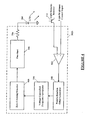
- a VFM pulse generator 202a comprises a one-shot 306 having a fixed pulse width (logic high time duration) output, a pulse on-time integrator 314, an operational amplifier 312 having differential inputs, a voltage controlled frequency generator 310, and a zero-crossing detector 308.
- the one-shot 306 is "fired" (output goes to a logic high for the fixed time duration) whenever a start pulse at its input is detected.
- These start pulses are supplied from the zero-crossing detector 308 at a repetition rate (pulses per time duration) which is determined from the frequency of the voltage controlled frequency generator 310.
- the voltage controlled frequency generator 310 may be a voltage controlled oscillator (VCO), voltage-to-frequency converter, etc.
- a resistor 316 is used to control the amount of current to the LED 204.
- the output frequency of the voltage controlled frequency generator 310 is controlled by a voltage from the operational amplifier 312.
- the operational amplifier 312 compares a light brightness voltage input with a voltage from the pulse on-time integrator 314.
- the voltage from the pulse on-time integrator 314 is representative of the percent that the output of the one-shot 306 is on during the certain time duration.
- the operational amplifier 312 has gain and will cause the voltage controlled frequency generator 310 to adjust its frequency so that the "on" time of the pulse train over a certain time duration equals the light brightness voltage input (voltage levels configured to be proportional to percent LED brightness). This arrangement produces a closed loop brightness control for the LED.
- an optional further feature may use a pseudo random offset generator 318 to introduce random voltage perturbations at the voltage input of the voltage controlled frequency generator 310. These random voltage perturbations may further spread EMI noise power over a greater (wider) number of frequencies, and thus reduce the EMI noise power at any one frequency. This is very advantageous when having to meet strict EMI radiation standards.
- the pseudo random offset generator 318 may be coupled between the pulse on-time integrator 314 and the operational amplifier 312, between the light brightness input and the operational amplifier 312, or between the operational amplifier 312 output and the voltage input of the voltage controlled frequency generator 310.
- the pseudo-random offset generator 318 may provide additional frequencies to those frequencies resulting from the combination of the light brightness closed loop control and output from the pulse on-time integrator 314.
- the light intensity input may be directly coupled to the voltage input of the voltage controlled frequency generator 310 and thus control the number of pulses per time duration results in the percent light brightness desired from the LED without regard to the pulse train on-time average. This arrangement produces an open loop brightness control for the LED.
- a VFM pulse generator 202b comprises a one-shot 306 having a fixed pulse width (logic high time duration) output, an operational amplifier 312 having differential inputs, a voltage controlled frequency generator 310, a zero-crossing detector 308, and a light brightness detector 414.
- the one-shot 306 is "fired" (output goes to a logic high for the fixed time duration) whenever a start pulse at its input is detected.
- These start pulses are supplied from the zero-crossing detector 308 at a repetition rate (pulses per time duration) which is determined from the frequency of the voltage controlled frequency generator 310.
- the voltage controlled frequency generator 310 may be a voltage controlled oscillator (VCO), voltage-to-frequency converter, etc.
- a resistor 316 is used to control the amount of current to the LED 204.
- the frequency of the voltage controlled frequency generator 310 is controlled by a voltage from the operational amplifier 312.
- the operational amplifier 312 compares a light intensity voltage input against a voltage from the light brightness detector 414.
- the voltage from the light intensity detector 414 is representative of the brightness of the LED 204.
- the operational amplifier 312 has gain and will cause the voltage controlled frequency generator 310 to adjust its frequency so that the brightness of the LED 204 equals the light brightness voltage input (voltage levels configured to be proportional to desired percent LED brightness).
- This arrangement produces a closed loop brightness control for the LED.
- An advantage of this configuration is that the pulses to the LED 204 may be adjusted to compensate for light brightness output degradation of the LED 204.
- an optional further feature may use a pseudo-random offset generator 318 to introduce random voltage perturbations at the voltage input of the voltage controlled frequency generator 310.
- pseudo-random voltage perturbations may further spread EMI noise power over a greater (wider) number of frequencies, and thus reduce the EMI noise power at any one frequency over time. This is very advantageous when having to meet strict EMI radiation standards.
- the pseudo random offset generator 318 may be coupled between the voltage input of the voltage controlled frequency generator 310 and the output of the operational amplifier 312, between the light brightness input and the operational amplifier 312, or between the light brightness detector 414 and an input of the operational amplifier 312.
- the pseudo-random offset generator 318 may provide additional frequencies to those frequencies resulting from the combination of the light intensity closed loop control and output from the light brightness detector 414.
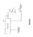
- a microcontroller 202c may be configured as a VFM pulse generator.
- the microcontroller 202c may have analog and/or digital inputs for control of light brightness and light intensity (brightness) detection from a light intensity detector 414.
- the microcontroller 202c generates the fixed pulse width (logic high time duration) output that drives the LED 204 through the current limiting resistor 316 with a software program.
- the number of fixed width pulses per time duration (frequency) is also controlled with the software program running in the microcontroller 202c.
Landscapes
- Circuit Arrangement For Electric Light Sources In General (AREA)
- Led Devices (AREA)
- Control Of Indicators Other Than Cathode Ray Tubes (AREA)
Applications Claiming Priority (4)
| Application Number | Priority Date | Filing Date | Title |
|---|---|---|---|
| US12197308P | 2008-12-12 | 2008-12-12 | |
| US12/576,346 US8339068B2 (en) | 2008-12-12 | 2009-10-09 | LED brightness control by variable frequency modulation |
| EP09768479.9A EP2377368B1 (de) | 2008-12-12 | 2009-12-11 | Led-helligkeitsregelung durch variable frequenzmodulation |
| PCT/US2009/067636 WO2010068845A1 (en) | 2008-12-12 | 2009-12-11 | Led brightness control by variable frequency modulation |
Related Parent Applications (2)
| Application Number | Title | Priority Date | Filing Date |
|---|---|---|---|
| EP09768479.9A Division EP2377368B1 (de) | 2008-12-12 | 2009-12-11 | Led-helligkeitsregelung durch variable frequenzmodulation |
| EP09768479.9A Division-Into EP2377368B1 (de) | 2008-12-12 | 2009-12-11 | Led-helligkeitsregelung durch variable frequenzmodulation |
Publications (3)
| Publication Number | Publication Date |
|---|---|
| EP2824994A2 true EP2824994A2 (de) | 2015-01-14 |
| EP2824994A3 EP2824994A3 (de) | 2015-03-11 |
| EP2824994B1 EP2824994B1 (de) | 2018-08-22 |
Family
ID=42239680
Family Applications (2)
| Application Number | Title | Priority Date | Filing Date |
|---|---|---|---|
| EP09768479.9A Active EP2377368B1 (de) | 2008-12-12 | 2009-12-11 | Led-helligkeitsregelung durch variable frequenzmodulation |
| EP14183301.2A Active EP2824994B1 (de) | 2008-12-12 | 2009-12-11 | Led-helligkeitssteuerung durch variable frequenzmodulation |
Family Applications Before (1)
| Application Number | Title | Priority Date | Filing Date |
|---|---|---|---|
| EP09768479.9A Active EP2377368B1 (de) | 2008-12-12 | 2009-12-11 | Led-helligkeitsregelung durch variable frequenzmodulation |
Country Status (6)
| Country | Link |
|---|---|
| US (1) | US8339068B2 (de) |
| EP (2) | EP2377368B1 (de) |
| KR (1) | KR101703080B1 (de) |
| CN (1) | CN102246592B (de) |
| TW (1) | TWI526118B (de) |
| WO (1) | WO2010068845A1 (de) |
Families Citing this family (17)
| Publication number | Priority date | Publication date | Assignee | Title |
|---|---|---|---|---|
| US20110241560A1 (en) * | 2010-04-01 | 2011-10-06 | Glp German Light Products Gmbh | Apparatus for generating a drive signal for a lamp device and method for generating a drive signal for a lamp device |
| WO2011120855A1 (en) * | 2010-04-01 | 2011-10-06 | Glp German Light Products Gmbh | Apparatus for generating a drive signal for a lamp device and method for generating a drive signal for a lamp device |
| DE102010015125A1 (de) * | 2010-04-16 | 2011-10-20 | Hella Kgaa Hueck & Co. | Verfahren zur Steuerung eines Lichtstroms einer Leuchteinrichtung mit einer Anzahl von Halbleiterleuchtmitteln, die zur Kennzeichnung und Markierung von Verkehrsflächen von Flughäfen eingerichtet ist |
| CN102387627B (zh) | 2010-09-03 | 2015-07-29 | 奥斯兰姆有限公司 | 发光二极管驱动及调光的方法和装置、以及照明系统 |
| US8890435B2 (en) * | 2011-03-11 | 2014-11-18 | Ilumi Solutions, Inc. | Wireless lighting control system |
| KR101361294B1 (ko) * | 2011-06-09 | 2014-02-11 | 한라비스테온공조 주식회사 | 차량용 공조 시스템에 적용되는 디스플레이 장치 및 그 장치의 제어방법 |
| US9554435B2 (en) | 2012-09-21 | 2017-01-24 | Texas Instruments Incorporated | LED drive apparatus, systems and methods |
| US9711092B2 (en) | 2013-03-14 | 2017-07-18 | Sharp Kabushiki Kaisha | Display device and method for driving same |
| KR102127853B1 (ko) * | 2013-12-31 | 2020-06-29 | 에스엘 주식회사 | 헤드업 디스플레이 장치 및 백라이트 유닛의 휘도 조절 방법 |
| US9585218B2 (en) * | 2014-08-21 | 2017-02-28 | Cree, Inc. | Lighting apparatus with variable current switching frequency and methods of operating same |
| CN106488621B (zh) | 2015-08-25 | 2021-02-12 | 西门子瑞士有限公司 | 通知设备 |
| DE202017002443U1 (de) * | 2017-05-08 | 2018-08-09 | Tridonic Gmbh & Co. Kg | Schaltungsanordnung zum Betreiben eines Leuchtmittels |
| TWI672074B (zh) * | 2018-06-15 | 2019-09-11 | 緯創資通股份有限公司 | 發光系統、控制裝置以及控制方法 |
| US11239399B2 (en) | 2019-02-05 | 2022-02-01 | Facebook Technologies, Llc | Architecture for hybrid TFT-based micro display projector |
| EP3829044B1 (de) * | 2019-11-29 | 2025-01-01 | Tridonic GmbH & Co. KG | Gemischte t_on-t_off-modulation für einen resonanzwandler |
| GB202015555D0 (en) * | 2020-10-01 | 2020-11-18 | Thermo Fisher Scient Bremen Gmbh | Determining the average frequency of a series of pulses |
| US11564296B2 (en) | 2021-02-12 | 2023-01-24 | Analog Devices International Unlimited Company | Stochastic frequency pulse modulation for light-emitting diode drivers |
Citations (2)
| Publication number | Priority date | Publication date | Assignee | Title |
|---|---|---|---|---|
| US20070103086A1 (en) | 2005-11-10 | 2007-05-10 | Neudorf Jason Christopher J | Modulation method and apparatus for dimming and/or colour mixing utilizing leds |
| WO2008056321A1 (en) | 2006-11-10 | 2008-05-15 | Koninklijke Philips Electronics N.V. | Method and driver for determining drive values for driving a lighting device |
Family Cites Families (8)
| Publication number | Priority date | Publication date | Assignee | Title |
|---|---|---|---|---|
| US5924784A (en) * | 1995-08-21 | 1999-07-20 | Chliwnyj; Alex | Microprocessor based simulated electronic flame |
| US6407515B1 (en) * | 1999-11-12 | 2002-06-18 | Lighting Control, Inc. | Power regulator employing a sinusoidal reference |
| KR20020048144A (ko) * | 2000-12-16 | 2002-06-22 | 양성석 | 초음파 진동맛사지기의 프로브 |
| WO2004057923A1 (en) | 2002-12-20 | 2004-07-08 | Koninklijke Philips Electronics N.V. | Sensing light emitted from multiple light sources |
| KR100925470B1 (ko) * | 2003-03-17 | 2009-11-06 | 삼성전자주식회사 | 액정 표시 장치 및 액정 표시 장치용 광원의 구동 장치 |
| US7119500B2 (en) * | 2003-12-05 | 2006-10-10 | Dialight Corporation | Dynamic color mixing LED device |
| JP4754280B2 (ja) * | 2005-06-24 | 2011-08-24 | 富士重工業株式会社 | 発光装置の輝度制御システム |
| US7315139B1 (en) * | 2006-11-30 | 2008-01-01 | Avago Technologis Ecbu Ip (Singapore) Pte Ltd | Light source having more than three LEDs in which the color points are maintained using a three channel color sensor |
-
2009
- 2009-10-09 US US12/576,346 patent/US8339068B2/en active Active
- 2009-12-11 EP EP09768479.9A patent/EP2377368B1/de active Active
- 2009-12-11 KR KR1020117004184A patent/KR101703080B1/ko active Active
- 2009-12-11 CN CN200980149568.7A patent/CN102246592B/zh active Active
- 2009-12-11 WO PCT/US2009/067636 patent/WO2010068845A1/en not_active Ceased
- 2009-12-11 EP EP14183301.2A patent/EP2824994B1/de active Active
- 2009-12-11 TW TW098142574A patent/TWI526118B/zh active
Patent Citations (2)
| Publication number | Priority date | Publication date | Assignee | Title |
|---|---|---|---|---|
| US20070103086A1 (en) | 2005-11-10 | 2007-05-10 | Neudorf Jason Christopher J | Modulation method and apparatus for dimming and/or colour mixing utilizing leds |
| WO2008056321A1 (en) | 2006-11-10 | 2008-05-15 | Koninklijke Philips Electronics N.V. | Method and driver for determining drive values for driving a lighting device |
Also Published As
| Publication number | Publication date |
|---|---|
| TWI526118B (zh) | 2016-03-11 |
| KR20110098707A (ko) | 2011-09-01 |
| CN102246592B (zh) | 2016-01-06 |
| CN102246592A (zh) | 2011-11-16 |
| EP2824994B1 (de) | 2018-08-22 |
| KR101703080B1 (ko) | 2017-02-06 |
| EP2377368A1 (de) | 2011-10-19 |
| WO2010068845A1 (en) | 2010-06-17 |
| TW201032669A (en) | 2010-09-01 |
| US20100148678A1 (en) | 2010-06-17 |
| US8339068B2 (en) | 2012-12-25 |
| EP2824994A3 (de) | 2015-03-11 |
| EP2377368B1 (de) | 2014-10-15 |
Similar Documents
| Publication | Publication Date | Title |
|---|---|---|
| EP2824994B1 (de) | Led-helligkeitssteuerung durch variable frequenzmodulation | |
| EP2368406B1 (de) | Dreiphasen-rgb-led-farbmischung und steuerung durch variable frequenzmodulation | |
| CA2564659C (en) | Modulation method and apparatus for dimming and/or colour mixing leds | |
| US8085106B2 (en) | Method and apparatus for dynamic modulation | |
| US8110997B2 (en) | LED drive circuit | |
| US10368410B2 (en) | PWM control for LEDs with reduced flicker when using spread spectrum switching frequencies | |
| EP2062356A1 (de) | Pwm-verfahren und vorrichtung sowie damit betriebene lichtquelle | |
| US11432385B2 (en) | Single comparator exponential-scale PWM dimming | |
| EP3030049B1 (de) | LED-Steuerungen, Treiber und Beleuchtungsschaltungen | |
| US20130154503A1 (en) | Method to control a lighting current of a lighting device | |
| JP6072802B2 (ja) | Ledドライバ | |
| EP3292740B1 (de) | Pulsweitenmodulationslichtquellenansteuerung und verfahren | |
| US20060232501A1 (en) | Method and apparatus for implementing a pulse skip method of controlling light intensity | |
| CN103081565B (zh) | 用于驱动至少一个发光二极管的方法和用于实施该方法的照明装置 |
Legal Events
| Date | Code | Title | Description |
|---|---|---|---|
| 17P | Request for examination filed |
Effective date: 20140902 |
|
| AC | Divisional application: reference to earlier application |
Ref document number: 2377368 Country of ref document: EP Kind code of ref document: P |
|
| AK | Designated contracting states |
Kind code of ref document: A2 Designated state(s): AT BE BG CH CY CZ DE DK EE ES FI FR GB GR HR HU IE IS IT LI LT LU LV MC MK MT NL NO PL PT RO SE SI SK SM TR |
|
| PUAI | Public reference made under article 153(3) epc to a published international application that has entered the european phase |
Free format text: ORIGINAL CODE: 0009012 |
|
| PUAL | Search report despatched |
Free format text: ORIGINAL CODE: 0009013 |
|
| AK | Designated contracting states |
Kind code of ref document: A3 Designated state(s): AT BE BG CH CY CZ DE DK EE ES FI FR GB GR HR HU IE IS IT LI LT LU LV MC MK MT NL NO PL PT RO SE SI SK SM TR |
|
| RIC1 | Information provided on ipc code assigned before grant |
Ipc: H05B 33/08 20060101AFI20150202BHEP |
|
| STAA | Information on the status of an ep patent application or granted ep patent |
Free format text: STATUS: EXAMINATION IS IN PROGRESS |
|
| 17Q | First examination report despatched |
Effective date: 20161206 |
|
| GRAP | Despatch of communication of intention to grant a patent |
Free format text: ORIGINAL CODE: EPIDOSNIGR1 |
|
| STAA | Information on the status of an ep patent application or granted ep patent |
Free format text: STATUS: GRANT OF PATENT IS INTENDED |
|
| INTG | Intention to grant announced |
Effective date: 20180313 |
|
| GRAS | Grant fee paid |
Free format text: ORIGINAL CODE: EPIDOSNIGR3 |
|
| GRAA | (expected) grant |
Free format text: ORIGINAL CODE: 0009210 |
|
| STAA | Information on the status of an ep patent application or granted ep patent |
Free format text: STATUS: THE PATENT HAS BEEN GRANTED |
|
| AC | Divisional application: reference to earlier application |
Ref document number: 2377368 Country of ref document: EP Kind code of ref document: P |
|
| AK | Designated contracting states |
Kind code of ref document: B1 Designated state(s): AT BE BG CH CY CZ DE DK EE ES FI FR GB GR HR HU IE IS IT LI LT LU LV MC MK MT NL NO PL PT RO SE SI SK SM TR |
|
| REG | Reference to a national code |
Ref country code: GB Ref legal event code: FG4D |
|
| REG | Reference to a national code |
Ref country code: CH Ref legal event code: EP |
|
| REG | Reference to a national code |
Ref country code: AT Ref legal event code: REF Ref document number: 1034020 Country of ref document: AT Kind code of ref document: T Effective date: 20180915 |
|
| REG | Reference to a national code |
Ref country code: IE Ref legal event code: FG4D |
|
| REG | Reference to a national code |
Ref country code: DE Ref legal event code: R096 Ref document number: 602009054096 Country of ref document: DE |
|
| REG | Reference to a national code |
Ref country code: NL Ref legal event code: MP Effective date: 20180822 |
|
| REG | Reference to a national code |
Ref country code: LT Ref legal event code: MG4D |
|
| PG25 | Lapsed in a contracting state [announced via postgrant information from national office to epo] |
Ref country code: SE Free format text: LAPSE BECAUSE OF FAILURE TO SUBMIT A TRANSLATION OF THE DESCRIPTION OR TO PAY THE FEE WITHIN THE PRESCRIBED TIME-LIMIT Effective date: 20180822 Ref country code: IS Free format text: LAPSE BECAUSE OF FAILURE TO SUBMIT A TRANSLATION OF THE DESCRIPTION OR TO PAY THE FEE WITHIN THE PRESCRIBED TIME-LIMIT Effective date: 20181222 Ref country code: NL Free format text: LAPSE BECAUSE OF FAILURE TO SUBMIT A TRANSLATION OF THE DESCRIPTION OR TO PAY THE FEE WITHIN THE PRESCRIBED TIME-LIMIT Effective date: 20180822 Ref country code: FI Free format text: LAPSE BECAUSE OF FAILURE TO SUBMIT A TRANSLATION OF THE DESCRIPTION OR TO PAY THE FEE WITHIN THE PRESCRIBED TIME-LIMIT Effective date: 20180822 Ref country code: LT Free format text: LAPSE BECAUSE OF FAILURE TO SUBMIT A TRANSLATION OF THE DESCRIPTION OR TO PAY THE FEE WITHIN THE PRESCRIBED TIME-LIMIT Effective date: 20180822 Ref country code: GR Free format text: LAPSE BECAUSE OF FAILURE TO SUBMIT A TRANSLATION OF THE DESCRIPTION OR TO PAY THE FEE WITHIN THE PRESCRIBED TIME-LIMIT Effective date: 20181123 Ref country code: NO Free format text: LAPSE BECAUSE OF FAILURE TO SUBMIT A TRANSLATION OF THE DESCRIPTION OR TO PAY THE FEE WITHIN THE PRESCRIBED TIME-LIMIT Effective date: 20181122 Ref country code: BG Free format text: LAPSE BECAUSE OF FAILURE TO SUBMIT A TRANSLATION OF THE DESCRIPTION OR TO PAY THE FEE WITHIN THE PRESCRIBED TIME-LIMIT Effective date: 20181122 |
|
| REG | Reference to a national code |
Ref country code: AT Ref legal event code: MK05 Ref document number: 1034020 Country of ref document: AT Kind code of ref document: T Effective date: 20180822 |
|
| PG25 | Lapsed in a contracting state [announced via postgrant information from national office to epo] |
Ref country code: HR Free format text: LAPSE BECAUSE OF FAILURE TO SUBMIT A TRANSLATION OF THE DESCRIPTION OR TO PAY THE FEE WITHIN THE PRESCRIBED TIME-LIMIT Effective date: 20180822 Ref country code: LV Free format text: LAPSE BECAUSE OF FAILURE TO SUBMIT A TRANSLATION OF THE DESCRIPTION OR TO PAY THE FEE WITHIN THE PRESCRIBED TIME-LIMIT Effective date: 20180822 |
|
| PG25 | Lapsed in a contracting state [announced via postgrant information from national office to epo] |
Ref country code: AT Free format text: LAPSE BECAUSE OF FAILURE TO SUBMIT A TRANSLATION OF THE DESCRIPTION OR TO PAY THE FEE WITHIN THE PRESCRIBED TIME-LIMIT Effective date: 20180822 Ref country code: PL Free format text: LAPSE BECAUSE OF FAILURE TO SUBMIT A TRANSLATION OF THE DESCRIPTION OR TO PAY THE FEE WITHIN THE PRESCRIBED TIME-LIMIT Effective date: 20180822 Ref country code: ES Free format text: LAPSE BECAUSE OF FAILURE TO SUBMIT A TRANSLATION OF THE DESCRIPTION OR TO PAY THE FEE WITHIN THE PRESCRIBED TIME-LIMIT Effective date: 20180822 Ref country code: EE Free format text: LAPSE BECAUSE OF FAILURE TO SUBMIT A TRANSLATION OF THE DESCRIPTION OR TO PAY THE FEE WITHIN THE PRESCRIBED TIME-LIMIT Effective date: 20180822 Ref country code: RO Free format text: LAPSE BECAUSE OF FAILURE TO SUBMIT A TRANSLATION OF THE DESCRIPTION OR TO PAY THE FEE WITHIN THE PRESCRIBED TIME-LIMIT Effective date: 20180822 Ref country code: IT Free format text: LAPSE BECAUSE OF FAILURE TO SUBMIT A TRANSLATION OF THE DESCRIPTION OR TO PAY THE FEE WITHIN THE PRESCRIBED TIME-LIMIT Effective date: 20180822 Ref country code: CZ Free format text: LAPSE BECAUSE OF FAILURE TO SUBMIT A TRANSLATION OF THE DESCRIPTION OR TO PAY THE FEE WITHIN THE PRESCRIBED TIME-LIMIT Effective date: 20180822 |
|
| REG | Reference to a national code |
Ref country code: DE Ref legal event code: R097 Ref document number: 602009054096 Country of ref document: DE |
|
| PG25 | Lapsed in a contracting state [announced via postgrant information from national office to epo] |
Ref country code: SM Free format text: LAPSE BECAUSE OF FAILURE TO SUBMIT A TRANSLATION OF THE DESCRIPTION OR TO PAY THE FEE WITHIN THE PRESCRIBED TIME-LIMIT Effective date: 20180822 Ref country code: DK Free format text: LAPSE BECAUSE OF FAILURE TO SUBMIT A TRANSLATION OF THE DESCRIPTION OR TO PAY THE FEE WITHIN THE PRESCRIBED TIME-LIMIT Effective date: 20180822 Ref country code: SK Free format text: LAPSE BECAUSE OF FAILURE TO SUBMIT A TRANSLATION OF THE DESCRIPTION OR TO PAY THE FEE WITHIN THE PRESCRIBED TIME-LIMIT Effective date: 20180822 |
|
| PLBE | No opposition filed within time limit |
Free format text: ORIGINAL CODE: 0009261 |
|
| STAA | Information on the status of an ep patent application or granted ep patent |
Free format text: STATUS: NO OPPOSITION FILED WITHIN TIME LIMIT |
|
| 26N | No opposition filed |
Effective date: 20190523 |
|
| REG | Reference to a national code |
Ref country code: CH Ref legal event code: PL |
|
| GBPC | Gb: european patent ceased through non-payment of renewal fee |
Effective date: 20181211 |
|
| PG25 | Lapsed in a contracting state [announced via postgrant information from national office to epo] |
Ref country code: SI Free format text: LAPSE BECAUSE OF FAILURE TO SUBMIT A TRANSLATION OF THE DESCRIPTION OR TO PAY THE FEE WITHIN THE PRESCRIBED TIME-LIMIT Effective date: 20180822 Ref country code: LU Free format text: LAPSE BECAUSE OF NON-PAYMENT OF DUE FEES Effective date: 20181211 Ref country code: MC Free format text: LAPSE BECAUSE OF FAILURE TO SUBMIT A TRANSLATION OF THE DESCRIPTION OR TO PAY THE FEE WITHIN THE PRESCRIBED TIME-LIMIT Effective date: 20180822 |
|
| REG | Reference to a national code |
Ref country code: IE Ref legal event code: MM4A |
|
| REG | Reference to a national code |
Ref country code: BE Ref legal event code: MM Effective date: 20181231 |
|
| PG25 | Lapsed in a contracting state [announced via postgrant information from national office to epo] |
Ref country code: IE Free format text: LAPSE BECAUSE OF NON-PAYMENT OF DUE FEES Effective date: 20181211 |
|
| REG | Reference to a national code |
Ref country code: DE Ref legal event code: R079 Ref document number: 602009054096 Country of ref document: DE Free format text: PREVIOUS MAIN CLASS: H05B0033080000 Ipc: H05B0045000000 |
|
| PG25 | Lapsed in a contracting state [announced via postgrant information from national office to epo] |
Ref country code: BE Free format text: LAPSE BECAUSE OF NON-PAYMENT OF DUE FEES Effective date: 20181231 |
|
| PG25 | Lapsed in a contracting state [announced via postgrant information from national office to epo] |
Ref country code: CH Free format text: LAPSE BECAUSE OF NON-PAYMENT OF DUE FEES Effective date: 20181231 Ref country code: GB Free format text: LAPSE BECAUSE OF NON-PAYMENT OF DUE FEES Effective date: 20181211 Ref country code: LI Free format text: LAPSE BECAUSE OF NON-PAYMENT OF DUE FEES Effective date: 20181231 |
|
| PG25 | Lapsed in a contracting state [announced via postgrant information from national office to epo] |
Ref country code: MT Free format text: LAPSE BECAUSE OF NON-PAYMENT OF DUE FEES Effective date: 20181211 |
|
| PG25 | Lapsed in a contracting state [announced via postgrant information from national office to epo] |
Ref country code: TR Free format text: LAPSE BECAUSE OF FAILURE TO SUBMIT A TRANSLATION OF THE DESCRIPTION OR TO PAY THE FEE WITHIN THE PRESCRIBED TIME-LIMIT Effective date: 20180822 |
|
| PG25 | Lapsed in a contracting state [announced via postgrant information from national office to epo] |
Ref country code: PT Free format text: LAPSE BECAUSE OF FAILURE TO SUBMIT A TRANSLATION OF THE DESCRIPTION OR TO PAY THE FEE WITHIN THE PRESCRIBED TIME-LIMIT Effective date: 20180822 |
|
| PG25 | Lapsed in a contracting state [announced via postgrant information from national office to epo] |
Ref country code: HU Free format text: LAPSE BECAUSE OF FAILURE TO SUBMIT A TRANSLATION OF THE DESCRIPTION OR TO PAY THE FEE WITHIN THE PRESCRIBED TIME-LIMIT; INVALID AB INITIO Effective date: 20091211 Ref country code: MK Free format text: LAPSE BECAUSE OF NON-PAYMENT OF DUE FEES Effective date: 20180822 Ref country code: CY Free format text: LAPSE BECAUSE OF FAILURE TO SUBMIT A TRANSLATION OF THE DESCRIPTION OR TO PAY THE FEE WITHIN THE PRESCRIBED TIME-LIMIT Effective date: 20180822 |
|
| P01 | Opt-out of the competence of the unified patent court (upc) registered |
Effective date: 20230528 |
|
| PGFP | Annual fee paid to national office [announced via postgrant information from national office to epo] |
Ref country code: DE Payment date: 20251126 Year of fee payment: 17 |
|
| PGFP | Annual fee paid to national office [announced via postgrant information from national office to epo] |
Ref country code: FR Payment date: 20251119 Year of fee payment: 17 |