EP2824836A2 - Cascode switch device - Google Patents
Cascode switch device Download PDFInfo
- Publication number
- EP2824836A2 EP2824836A2 EP14175711.2A EP14175711A EP2824836A2 EP 2824836 A2 EP2824836 A2 EP 2824836A2 EP 14175711 A EP14175711 A EP 14175711A EP 2824836 A2 EP2824836 A2 EP 2824836A2
- Authority
- EP
- European Patent Office
- Prior art keywords
- drain
- voltage transistor
- electrode
- capacitance
- source
- Prior art date
- Legal status (The legal status is an assumption and is not a legal conclusion. Google has not performed a legal analysis and makes no representation as to the accuracy of the status listed.)
- Withdrawn
Links
Images




Classifications
-
- H—ELECTRICITY
- H03—ELECTRONIC CIRCUITRY
- H03K—PULSE TECHNIQUE
- H03K17/00—Electronic switching or gating, i.e. not by contact-making and –breaking
- H03K17/08—Modifications for protecting switching circuit against overcurrent or overvoltage
- H03K17/081—Modifications for protecting switching circuit against overcurrent or overvoltage without feedback from the output circuit to the control circuit
- H03K17/08116—Modifications for protecting switching circuit against overcurrent or overvoltage without feedback from the output circuit to the control circuit in composite switches
-
- H—ELECTRICITY
- H10—SEMICONDUCTOR DEVICES; ELECTRIC SOLID-STATE DEVICES NOT OTHERWISE PROVIDED FOR
- H10D—INORGANIC ELECTRIC SEMICONDUCTOR DEVICES
- H10D84/00—Integrated devices formed in or on semiconductor substrates that comprise only semiconducting layers, e.g. on Si wafers or on GaAs-on-Si wafers
- H10D84/80—Integrated devices formed in or on semiconductor substrates that comprise only semiconducting layers, e.g. on Si wafers or on GaAs-on-Si wafers characterised by the integration of at least one component covered by groups H10D12/00 or H10D30/00, e.g. integration of IGFETs
- H10D84/82—Integrated devices formed in or on semiconductor substrates that comprise only semiconducting layers, e.g. on Si wafers or on GaAs-on-Si wafers characterised by the integration of at least one component covered by groups H10D12/00 or H10D30/00, e.g. integration of IGFETs of only field-effect components
- H10D84/83—Integrated devices formed in or on semiconductor substrates that comprise only semiconducting layers, e.g. on Si wafers or on GaAs-on-Si wafers characterised by the integration of at least one component covered by groups H10D12/00 or H10D30/00, e.g. integration of IGFETs of only field-effect components of only insulated-gate FETs [IGFET]
- H10D84/84—Combinations of enhancement-mode IGFETs and depletion-mode IGFETs
-
- H—ELECTRICITY
- H03—ELECTRONIC CIRCUITRY
- H03K—PULSE TECHNIQUE
- H03K17/00—Electronic switching or gating, i.e. not by contact-making and –breaking
- H03K17/08—Modifications for protecting switching circuit against overcurrent or overvoltage
- H03K17/082—Modifications for protecting switching circuit against overcurrent or overvoltage by feedback from the output to the control circuit
- H03K17/0828—Modifications for protecting switching circuit against overcurrent or overvoltage by feedback from the output to the control circuit in composite switches
-
- H—ELECTRICITY
- H03—ELECTRONIC CIRCUITRY
- H03K—PULSE TECHNIQUE
- H03K17/00—Electronic switching or gating, i.e. not by contact-making and –breaking
- H03K17/10—Modifications for increasing the maximum permissible switched voltage
- H03K17/102—Modifications for increasing the maximum permissible switched voltage in field-effect transistor switches
-
- H—ELECTRICITY
- H03—ELECTRONIC CIRCUITRY
- H03K—PULSE TECHNIQUE
- H03K17/00—Electronic switching or gating, i.e. not by contact-making and –breaking
- H03K17/51—Electronic switching or gating, i.e. not by contact-making and –breaking characterised by the components used
- H03K17/56—Electronic switching or gating, i.e. not by contact-making and –breaking characterised by the components used by the use, as active elements, of semiconductor devices
- H03K17/687—Electronic switching or gating, i.e. not by contact-making and –breaking characterised by the components used by the use, as active elements, of semiconductor devices the devices being field-effect transistors
- H03K2017/6875—Electronic switching or gating, i.e. not by contact-making and –breaking characterised by the components used by the use, as active elements, of semiconductor devices the devices being field-effect transistors using self-conductive, depletion FETs
Definitions
- the present invention relates to a technology of an electronic circuitry. More particularly, the present invention relates to a cascode switch device.
- a normally-on device can be cascaded with a low voltage device to produce an enhancement mode cascode switch device.
- the utility and durability of such a cascode switch device can be limited according to the characteristics of the low voltage device included therein.
- the durability of the cascode switch device may be limited by the breakdown voltage of the low voltage device.
- the cascode switch device should be configured to provide a voltage protection mechanism for the low voltage device.
- An object of the present invention is to provide a cascode switch device.
- the cascode switch device includes a high voltage (HV) transistor and a low voltage (LV) transistor.
- the high voltage transistor has a first drain electrode, a first source electrode, and a first gate electrode.
- the low voltage transistor has a second drain electrode, a second source electrode, and a second gate electrode, the low voltage transistor cascoded with the high voltage transistor such that the first source electrode is electrically connected to the second drain electrode.
- the casode switch device has a first drain-to-source capacitance between the first source electrode and the first drain electrode, a gate-to-source capacitance between the first gate electrode and a first source electrode, a second drain-to-source capacitance between the second drain electrode and the second source electrode, and a gate-to-drain capacitance between the second gate electrode and the second drain electrode.
- a first ratio of an equivalent capacitance of the second drain-to-source capacitance, the gate-to-drain capacitance and the gate-to-source capacitance to the first drain-to-source capacitance being based on a second ratio of a drain voltage of the high voltage transistor to a break-down voltage of the low voltage transistor so as to provide voltage protection for the low voltage transistor.
- the cascode switch device includes a normally-on high voltage transistor and a normally-off low voltage transistor.
- the normally-on high voltage transistor has a first drain electrode, a first source electrode, and a first gate electrode.
- the normally-off low voltage transistor has a second drain electrode, a second source electrode, and a second gate electrode, the normally-off low voltage transistor cascoded with the normally-on high voltage transistor.
- the casode switch device has a first drain-to-source capacitance between the first source electrode and the first drain electrode, a gate-to-source capacitance between the first gate electrode and a first source electrode, a second drain-to-source capacitance between the second drain electrode and the second source electrode, and a gate-to-drain capacitance between the second gate electrode and the second drain electrode.
- a first ratio of an equivalent capacitance of the second drain-to-source capacitance, the gate-to-drain capacitance and the gate-to-source capacitance to the first drain-to-source capacitance being based on a second ratio of a drain voltage of the normally-on high voltage transistor to a break-down voltage of the normally-off low voltage transistor so as to provide voltage protection for the normally-off low voltage transistor.
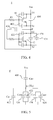
- FIG. 1 is diagram of a circuit diagram of a cascode switch device 1 in an embodiment of the present invention.
- the cascode switch device 1 includes a high voltage (HV) transistor 10 and a low voltage (LV) transistor 12.
- the high voltage transistor 10 is a III-nitride power transistor that may comprise an active layer formed of a plurality of stacked nitride-based semiconductor layers, such as a gallium nitride (GaN) layer and a alumin gallium nitride (AlGaN) layer stacked on the gallium nitride layer, and may be implemented as an insulated-gate FET (IGFET) or as a heterostructure FET (HFET), for example.
- the III-nitride power transistor may be formed of a metal-insulator-semiconductor FET, such as a metal-oxide-semiconductor FET (MOSFET).
- MOSFET metal-oxide-semiconductor FET
- the high voltage transistor 10 may be configured to sustain a drain voltage of approximately 600V and having a gate rating of approximately 40V.
- the low voltage transistor 12 is a silicon-based or a nitride-based field-effect transistor. Moreover, in an embodiment, the low voltage transistor 12 is a nitride-based transistor, e.g. a nitride-based FET and the high voltage transistor 10 and the low voltage transistor 12 are monolithically formed on a same substrate. In another embodiment, the high voltage transistor 10 and the low voltage transistor 12 are located on different chips and packaged in one packaging device.
- the high voltage transistor 10 is a normally-on device and the low voltage transistor 12 is a normally-off device.
- the high voltage transistor 10 includes a first drain electrode D1, a first source electrode S1 and a first gate electrode G1.
- the low voltage transistor 12 includes a second drain electrode D2, a second source electrode S2 and a second gate electrode G2.
- the first drain electrode D1 of the high voltage transistor 10 is electrically connected to a system voltage Vss.
- the first source electrode S1 of the high voltage transistor 10 is electrically connected to the second drain electrode D2 of the low voltage transistor 12 at node P.
- the first gate electrode G1 of the high voltage transistor 10 is electrically connected to the second source electrode S2 of the low voltage transistor 12.
- the first gate electrode G1 is electrically connected to the second source electrode S2 through a resistor R1, as illustrated in FIG. 1 .
- the second gate electrode G2 of the low voltage transistor 12 receives a control signal C for controlling the operation of the cascode switch device 1.
- the material, the structure and the related parameters mentioned above are merely an example.
- the high voltage transistor 10 and the low voltage transistor 12 may be formed by using other material, structures and parameters.
- the high voltage transistor 10 and the low voltage transistor 12 can be both nitride-based FETs.
- the cascade switch device 1 is described by reference to specific, but merely exemplary parameters.
- the high voltage transistor 10 when the high voltage transistor 10 is on, a few volts will develop across the low voltage transistor 12. The voltage is thus inverted and applied to the first gate electrode G1 of the high voltage transistor 10.
- the high voltage transistor 10 will turn off and any additional increase in the voltage of the first drain electrode D1 will be sustained across the first drain electrode D1 and the first source electrode S1 of the high voltage transistor 10. Consequently, the low voltage transistor 12 will typically not be require to sustain a voltage beyond the few volts mentioned above.
- the voltage at the second drain electrode D2 of the low voltage transistor 12 will not rise beyond the rated breakdown voltage of the low voltage transistor 12 (e.g., approximately 30V to 40V).
- FIG. 2 is a diagram of a more detail representation of the cascode switch device 1 illustrated in FIG. 1 .
- the high voltage transistor 10 has a first drain-to-source capacitance Cds1 between the first source electrode S1 and the first drain electrode D1.
- the first drain-to-source capacitance Cds1 can be either contributed by an internal capacitance of the high voltage transistor 10, or contributed by the internal capacitance of the high voltage transistor 10 together with at least one external electronic component.
- the first drain-to-source capacitance Cds1 is contributed by an internal capacitance Cds_gan of a drain-to-source equivalent capacitor 100 of the high voltage transistor 10.
- the high voltage transistor 10 has a gate-to-source capacitance Cgs between the first source electrode S1 and the first gate electrode G1.
- the gate-to-source capacitance Cgs can be either contributed by an internal capacitance of the high voltage transistor 10, or contributed by the internal capacitance of the high voltage transistor 10 together with at least one external electronic component.
- the gate-to-source capacitance Cgs is contributed by an internal capacitance Cgs_gan of a gate-to-source equivalent capacitor 102 of the high voltage transistor 10.
- the low voltage transistor 12 has a second drain-to-source capacitance Cds2 between the second source electrode S2 and the second drain electrode D2.
- the second drain-to-source capacitance Cds2 can be either contributed by an internal capacitance of the low voltage transistor 12, or contributed by the internal capacitance of the low voltage transistor 12 together with at least one external electronic component.
- the second drain-to-source capacitance Cds2 is contributed by an internal capacitance Cds_si of a drain-to-source equivalent capacitor 120 of the low voltage transistor 12.
- the low voltage transistor 12 has a gate-to-drain capacitance Cgd between the second gate electrode G2 and the second drain electrode D2.
- the gate-to-drain capacitance Cgd can be either contributed by an internal capacitance of the low voltage transistor 12, or contributed by the internal capacitance of the low voltage transistor 12 together with at least one external electronic component.
- the gate-to-drain capacitance Cgd is contributed by an internal capacitance Cgd_si of a gate-to-drain equivalent capacitor 122 of the low voltage transistor 12.
- FIG. 3 is a diagram of an equivalent circuit 3 of the capacitors in FIG. 2 in an embodiment of the present invention.
- the capacitances of these capacitors are labeled.
- the equivalent capacitance of the lower part of the equivalent circuit 3 is equal to the sum of the second drain-to-source capacitance Cds2, the gate-to-drain capacitance Cgd and the gate-to-source capacitance Cgs, which is C ds 2 + C gd + C gs .
- the equivalent capacitance of the upper part of the equivalent circuit 3 is equal to the first drain-to-source capacitance Cds1.
- the voltage Vp at the point P, where the second drain electrode D2 of the low voltage transistor 12 is connected to is set by the ratio between the equivalent capacitances of the upper and the lower part of the equivalent circuit 3: V p ⁇ C ds ⁇ 1 / C ds ⁇ 2 + C gd + C gs * V ss
- a first ratio of the equivalent capacitance of the second drain-to-source capacitance Cds2, the gate-to-drain capacitance Cgd and the gate-to-source capacitance Cgs to the first drain-to-source capacitance Cds1 is based on a second ratio of the drain voltage Vss of the high voltage transistor 10 to a break-down voltage Vbr of the low voltage transistor 12 so as to provide voltage protection for the low voltage transistor 12, in which the break-down voltage Vbr of the low voltage transistor 12 is the highest tolerable voltage at the node P that keeps the low voltage transistor 12 from the breakdown condition.
- the relation between the first ratio and the second ratio is expressed by: C ds ⁇ 2 + C gd + C gs / C ds ⁇ 1 > V ss - V br / V br + V th_HV
- the system voltage Vss ranges from 100V to 1200V.
- the break-down voltage Vbr ranges from 30V to 40V and the threshold voltage Vth_HV of the high voltage transistor 10 ranges from -20V to 5V.
- the range of the first ratio is expressed by: 5 ⁇ C ds ⁇ 2 + C gd + C gs / C ds ⁇ 1 ⁇ 120 ,
- the first ratio is less than approximately 120 and is larger than approximately 5.
- the cascode switch device 1 illustrated in FIG. 1 having the first ratio of the equivalent capacitances being based on the second ratio of the drain voltage Vss of the high voltage transistor 10 to the break-down voltage Vbr of the low voltage transistor 12 provides the voltage protection for the low voltage transistor 12.
- FIG. 4 is a cascode switch device 4 in an embodiment of the present invention. Similar to the cascode switch device 1 illustrated in FIG. 1 and FIG. 2 , the cascode switch device 4 includes a high voltage transistor 40 and a low voltage transistor 42.
- the high voltage transistor 40 and the low voltage transistor 42 are substantially the same as the high voltage transistor 10 and the low voltage transistor 12 illustrated in FIG. 2 , in which the high voltage transistor 40 includes a drain-to-source equivalent capacitor 400 and a gate-to-source equivalent capacitor 402, and the low voltage transistor 42 includes a drain-to-source equivalent capacitor 420 and a gate-to-drain equivalent capacitor 422. Therefore, no further detail is discussed herein.
- the cascode switch device 4 further includes a first additional capacitor 424 and a second additional capacitor 426.
- the first additional capacitor 424 is connected between the second drain electrode D2 and the second source electrode S2 of the low voltage transistor 42.
- the second additional capacitor 426 is connected between the second gate electrode G2 and the second drain electrode D2 of the low voltage transistor 42.
- FIG. 5 is a diagram of an equivalent circuit 4 of the capacitors in FIG. 4 in an embodiment of the present invention.
- the capacitances of these capacitors are labeled.
- the second drain-to-source capacitance Cds2 is contributed by the internal capacitance Cds_si of a drain-to-source equivalent capacitor 420 of the low voltage transistor 42 and a capacitance Cadd1 of the first additional capacitor 424.
- the gate-to-drain capacitance Cgd is contributed the internal capacitance Cgd_si of the gate-to-drain equivalent capacitor 422 and a capacitance Cadd2 of the second additional capacitor 426.
- the first additional capacitor 424 and the second additional capacitor 426 can be used to meet the requirement.
- FIG. 6 is a cascode switch device 6 in an embodiment of the present invention. Similar to the cascode switch device 1 illustrated in FIG. 1 and in FIG. 2 , the cascode switch device 6 includes a high voltage transistor 60 and a low voltage transistor 62.
- the high voltage transistor 60 and the low voltage transistor 62 are substantially the same as the high voltage transistor 10 and the low voltage transistor 12 illustrated in FIG. 2 , in which the high voltage transistor 60 includes a drain-to-source equivalent capacitor 600 and a gate-to-source equivalent capacitor 602, and the low voltage transistor 62 includes a drain-to-source equivalent capacitor 620 and a gate-to-drain equivalent capacitor 622. Therefore, no further detail is discussed herein.
- the cascode switch device 6 further includes a first additional resistor 624 and a second additional resistor 626.
- the first additional capacitor 624 is connected between the second drain electrode D2 and the second source electrode S2 of the low voltage transistor 62.
- the second additional capacitor 626 is connected between the second gate electrode G2 and the second drain electrode D2 of the low voltage transistor 42.
- the low voltage transistor 12 may suffer from the breakdown condition due to the voltage Vp at the point P that increases dramatically when the low voltage transistor 12 turns off. Therefore, the first additional resistor 624 provides a current discharging mechanism.
- the off-resistance of the low voltage transistor 12 needs to be larger than the resistance of the first additional resistor 624.
- the on-resistance of the low voltage transistor 12 needs to be smaller than the resistance of the first additional resistor 624.
- the second additional resistor 626 provides the similar function as the first additional resistor 624. Therefore, no further detail is discussed herein.
- FIG. 7 is a cascode switch device 7 in an embodiment of the present invention. Similar to the cascode switch device 1 illustrated in FIG. 1 and in FIG. 2 , the cascode switch device 7 includes a high voltage transistor 70 and a low voltage transistor 72.
- the high voltage transistor 70 and the low voltage transistor 72 are substantially the same as the high voltage transistor 10 and the low voltage transistor 12 illustrated in FIG. 2 , in which the high voltage transistor 70 includes a drain-to-source equivalent capacitor 700 and a gate-to-source equivalent capacitor 702, and the low voltage transistor 72 includes a drain-to-source equivalent capacitor 720 and a gate-to-drain equivalent capacitor 722. Therefore, no further detail is discussed herein.
- the cascode switch device 7 further includes the first additional capacitor 424 and the second additional capacitor 426 illustrated in FIG. 4 and the first additional resistor 624 and the second additional resistor 626 illustrated in FIG. 6 . Therefore, the cascode switch device 7 can meet the requirement mentioned above by using the first additional capacitor 424 and the second additional capacitor 426 and perform the current discharging mechanism by using the first additional resistor 624 and the second additional resistor 626.
- the number of the additional capacitors and the additional resistors can be different according to the practical conditions and is not limited by the embodiments mentioned above.
Landscapes
- Electronic Switches (AREA)
- Amplifiers (AREA)
- Semiconductor Integrated Circuits (AREA)
Abstract
Description
- The present invention relates to a technology of an electronic circuitry. More particularly, the present invention relates to a cascode switch device.
- In power management applications, a normally-on device can be cascaded with a low voltage device to produce an enhancement mode cascode switch device. However, the utility and durability of such a cascode switch device can be limited according to the characteristics of the low voltage device included therein. For example, the durability of the cascode switch device may be limited by the breakdown voltage of the low voltage device. In order to render such cascode switch devices suitable for operation in power management systems, where high voltage spikes may present, the cascode switch device should be configured to provide a voltage protection mechanism for the low voltage device.
- Accordingly, what is needed is a cascode switch device to address the above issues.
- An object of the present invention is to provide a cascode switch device. The cascode switch device includes a high voltage (HV) transistor and a low voltage (LV) transistor. The high voltage transistor has a first drain electrode, a first source electrode, and a first gate electrode. The low voltage transistor has a second drain electrode, a second source electrode, and a second gate electrode, the low voltage transistor cascoded with the high voltage transistor such that the first source electrode is electrically connected to the second drain electrode. The casode switch device has a first drain-to-source capacitance between the first source electrode and the first drain electrode, a gate-to-source capacitance between the first gate electrode and a first source electrode, a second drain-to-source capacitance between the second drain electrode and the second source electrode, and a gate-to-drain capacitance between the second gate electrode and the second drain electrode. A first ratio of an equivalent capacitance of the second drain-to-source capacitance, the gate-to-drain capacitance and the gate-to-source capacitance to the first drain-to-source capacitance being based on a second ratio of a drain voltage of the high voltage transistor to a break-down voltage of the low voltage transistor so as to provide voltage protection for the low voltage transistor.
- Another aspect of the present invention is to provide a cascode switch device. The cascode switch device includes a normally-on high voltage transistor and a normally-off low voltage transistor. The normally-on high voltage transistor has a first drain electrode, a first source electrode, and a first gate electrode. The normally-off low voltage transistor has a second drain electrode, a second source electrode, and a second gate electrode, the normally-off low voltage transistor cascoded with the normally-on high voltage transistor. The casode switch device has a first drain-to-source capacitance between the first source electrode and the first drain electrode, a gate-to-source capacitance between the first gate electrode and a first source electrode, a second drain-to-source capacitance between the second drain electrode and the second source electrode, and a gate-to-drain capacitance between the second gate electrode and the second drain electrode. A first ratio of an equivalent capacitance of the second drain-to-source capacitance, the gate-to-drain capacitance and the gate-to-source capacitance to the first drain-to-source capacitance being based on a second ratio of a drain voltage of the normally-on high voltage transistor to a break-down voltage of the normally-off low voltage transistor so as to provide voltage protection for the normally-off low voltage transistor.
- These and other features, aspects, and advantages of the present invention will become better understood with reference to the following description and appended claims.
- It is to be understood that both the foregoing general description and the following detailed description are by examples, and are intended to provide further explanation of the invention as claimed.
- The invention can be more fully understood by reading the following detailed description of the embodiment, with reference made to the accompanying drawings as follows:
-
FIG. 1 is diagram of a circuit diagram of a cascode switch device in an embodiment of the present invention; -
FIG. 2 is a diagram of a more detail representation of the cascode switch device illustrated inFIG. 1 ; -
FIG. 3 is a diagram of an equivalent circuit of the capacitors inFIG. 2 in an embodiment of the present invention; -
FIG. 4 is a diagram of a circuit diagram of a cascode switch device in an embodiment of the present invention; -
FIG. 5 is a diagram of an equivalent circuit of the capacitors inFIG. 4 in an embodiment of the present invention; -
FIG. 6 is a diagram of a circuit diagram of a cascode switch device in an embodiment of the present invention; and -
FIG. 7 is a diagram of a circuit diagram of a cascode switch device in an embodiment of the present invention. - Reference will now be made in detail to the present embodiments of the invention, examples of which are illustrated in the accompanying drawings. Wherever possible, the same reference numbers are used in the drawings and the description to refer to the same or like parts.
-
FIG. 1 is diagram of a circuit diagram of acascode switch device 1 in an embodiment of the present invention. Thecascode switch device 1 includes a high voltage (HV)transistor 10 and a low voltage (LV)transistor 12. - In an embodiment, the
high voltage transistor 10 is a III-nitride power transistor that may comprise an active layer formed of a plurality of stacked nitride-based semiconductor layers, such as a gallium nitride (GaN) layer and a alumin gallium nitride (AlGaN) layer stacked on the gallium nitride layer, and may be implemented as an insulated-gate FET (IGFET) or as a heterostructure FET (HFET), for example. In an embodiment, the III-nitride power transistor may be formed of a metal-insulator-semiconductor FET, such as a metal-oxide-semiconductor FET (MOSFET). Moreover, in an embodiment, thehigh voltage transistor 10 may be configured to sustain a drain voltage of approximately 600V and having a gate rating of approximately 40V. - In an embodiment, the
low voltage transistor 12 is a silicon-based or a nitride-based field-effect transistor. Moreover, in an embodiment, thelow voltage transistor 12 is a nitride-based transistor, e.g. a nitride-based FET and thehigh voltage transistor 10 and thelow voltage transistor 12 are monolithically formed on a same substrate. In another embodiment, thehigh voltage transistor 10 and thelow voltage transistor 12 are located on different chips and packaged in one packaging device. - In an embodiment, the
high voltage transistor 10 is a normally-on device and thelow voltage transistor 12 is a normally-off device. - As illustrated in
FIG. 1 , thehigh voltage transistor 10 includes a first drain electrode D1, a first source electrode S1 and a first gate electrode G1. Thelow voltage transistor 12 includes a second drain electrode D2, a second source electrode S2 and a second gate electrode G2. The first drain electrode D1 of thehigh voltage transistor 10 is electrically connected to a system voltage Vss. The first source electrode S1 of thehigh voltage transistor 10 is electrically connected to the second drain electrode D2 of thelow voltage transistor 12 at node P. In an embodiment of the invention, the first gate electrode G1 of thehigh voltage transistor 10 is electrically connected to the second source electrode S2 of thelow voltage transistor 12. In an embodiment, the first gate electrode G1 is electrically connected to the second source electrode S2 through a resistor R1, as illustrated inFIG. 1 . - In an embodiment, the second gate electrode G2 of the
low voltage transistor 12 receives a control signal C for controlling the operation of thecascode switch device 1. - It is noted that the material, the structure and the related parameters mentioned above are merely an example. In other embodiments, the
high voltage transistor 10 and thelow voltage transistor 12 may be formed by using other material, structures and parameters. For example, in an embodiment, thehigh voltage transistor 10 and thelow voltage transistor 12 can be both nitride-based FETs. - The operation of the
cascade switch device 1 is described by reference to specific, but merely exemplary parameters. For example, when thehigh voltage transistor 10 is on, a few volts will develop across thelow voltage transistor 12. The voltage is thus inverted and applied to the first gate electrode G1 of thehigh voltage transistor 10. In response, thehigh voltage transistor 10 will turn off and any additional increase in the voltage of the first drain electrode D1 will be sustained across the first drain electrode D1 and the first source electrode S1 of thehigh voltage transistor 10. Consequently, thelow voltage transistor 12 will typically not be require to sustain a voltage beyond the few volts mentioned above. - In order to provide effective voltage protection for
low voltage transistor 12, it is important to more reliably establish that the voltage at the second drain electrode D2 of thelow voltage transistor 12 will not rise beyond the rated breakdown voltage of the low voltage transistor 12 (e.g., approximately 30V to 40V). -
FIG. 2 is a diagram of a more detail representation of thecascode switch device 1 illustrated inFIG. 1 . - The
high voltage transistor 10 has a first drain-to-source capacitance Cds1 between the first source electrode S1 and the first drain electrode D1. The first drain-to-source capacitance Cds1 can be either contributed by an internal capacitance of thehigh voltage transistor 10, or contributed by the internal capacitance of thehigh voltage transistor 10 together with at least one external electronic component. In the present embodiment, the first drain-to-source capacitance Cds1 is contributed by an internal capacitance Cds_gan of a drain-to-sourceequivalent capacitor 100 of thehigh voltage transistor 10. - Moreover, the
high voltage transistor 10 has a gate-to-source capacitance Cgs between the first source electrode S1 and the first gate electrode G1. Similarly, the gate-to-source capacitance Cgs can be either contributed by an internal capacitance of thehigh voltage transistor 10, or contributed by the internal capacitance of thehigh voltage transistor 10 together with at least one external electronic component. In the present embodiment, the gate-to-source capacitance Cgs is contributed by an internal capacitance Cgs_gan of a gate-to-sourceequivalent capacitor 102 of thehigh voltage transistor 10. - The
low voltage transistor 12 has a second drain-to-source capacitance Cds2 between the second source electrode S2 and the second drain electrode D2. Similarly, the second drain-to-source capacitance Cds2 can be either contributed by an internal capacitance of thelow voltage transistor 12, or contributed by the internal capacitance of thelow voltage transistor 12 together with at least one external electronic component. In the present embodiment, the second drain-to-source capacitance Cds2 is contributed by an internal capacitance Cds_si of a drain-to-sourceequivalent capacitor 120 of thelow voltage transistor 12. - Moreover, the
low voltage transistor 12 has a gate-to-drain capacitance Cgd between the second gate electrode G2 and the second drain electrode D2. Similarly, the gate-to-drain capacitance Cgd can be either contributed by an internal capacitance of thelow voltage transistor 12, or contributed by the internal capacitance of thelow voltage transistor 12 together with at least one external electronic component. In the present embodiment, the gate-to-drain capacitance Cgd is contributed by an internal capacitance Cgd_si of a gate-to-drainequivalent capacitor 122 of thelow voltage transistor 12. -
FIG. 3 is a diagram of anequivalent circuit 3 of the capacitors inFIG. 2 in an embodiment of the present invention. InFIG. 3 , the capacitances of these capacitors are labeled. - In an embodiment, the equivalent capacitance of the lower part of the
equivalent circuit 3 is equal to the sum of the second drain-to-source capacitance Cds2, the gate-to-drain capacitance Cgd and the gate-to-source capacitance Cgs, which is C ds2 + Cgd + Cgs. Moreover, the equivalent capacitance of the upper part of theequivalent circuit 3 is equal to the first drain-to-source capacitance Cds1. - During the transient operation, the voltage Vp at the point P, where the second drain electrode D2 of the
low voltage transistor 12 is connected to, is set by the ratio between the equivalent capacitances of the upper and the lower part of the equivalent circuit 3:
- Accordingly, in an embodiment, a first ratio of the equivalent capacitance of the second drain-to-source capacitance Cds2, the gate-to-drain capacitance Cgd and the gate-to-source capacitance Cgs to the first drain-to-source capacitance Cds1 is based on a second ratio of the drain voltage Vss of the
high voltage transistor 10 to a break-down voltage Vbr of thelow voltage transistor 12 so as to provide voltage protection for thelow voltage transistor 12, in which the break-down voltage Vbr of thelow voltage transistor 12 is the highest tolerable voltage at the node P that keeps thelow voltage transistor 12 from the breakdown condition. - If the threshold voltage Vth_HV of the
high voltage transistor 10 is considered, the relation between the first ratio and the second ratio is expressed by:
- In an embodiment, the system voltage Vss ranges from 100V to 1200V. The break-down voltage Vbr ranges from 30V to 40V and the threshold voltage Vth_HV of the
high voltage transistor 10 ranges from -20V to 5V. Under such a condition, the range of the first ratio is expressed by:
- in which the first ratio is less than approximately 120 and is larger than approximately 5.
- Consequently, the
cascode switch device 1 illustrated inFIG. 1 having the first ratio of the equivalent capacitances being based on the second ratio of the drain voltage Vss of thehigh voltage transistor 10 to the break-down voltage Vbr of thelow voltage transistor 12 provides the voltage protection for thelow voltage transistor 12. -
FIG. 4 is acascode switch device 4 in an embodiment of the present invention. Similar to thecascode switch device 1 illustrated inFIG. 1 andFIG. 2 , thecascode switch device 4 includes ahigh voltage transistor 40 and alow voltage transistor 42. - The
high voltage transistor 40 and thelow voltage transistor 42 are substantially the same as thehigh voltage transistor 10 and thelow voltage transistor 12 illustrated inFIG. 2 , in which thehigh voltage transistor 40 includes a drain-to-sourceequivalent capacitor 400 and a gate-to-sourceequivalent capacitor 402, and thelow voltage transistor 42 includes a drain-to-sourceequivalent capacitor 420 and a gate-to-drainequivalent capacitor 422. Therefore, no further detail is discussed herein. - In the present embodiment, the
cascode switch device 4 further includes a firstadditional capacitor 424 and a secondadditional capacitor 426. The firstadditional capacitor 424 is connected between the second drain electrode D2 and the second source electrode S2 of thelow voltage transistor 42. The secondadditional capacitor 426 is connected between the second gate electrode G2 and the second drain electrode D2 of thelow voltage transistor 42. -
FIG. 5 is a diagram of anequivalent circuit 4 of the capacitors inFIG. 4 in an embodiment of the present invention. InFIG. 5 , the capacitances of these capacitors are labeled. - As a result, the second drain-to-source capacitance Cds2 is contributed by the internal capacitance Cds_si of a drain-to-source
equivalent capacitor 420 of thelow voltage transistor 42 and a capacitance Cadd1 of the firstadditional capacitor 424. The gate-to-drain capacitance Cgd is contributed the internal capacitance Cgd_si of the gate-to-drainequivalent capacitor 422 and a capacitance Cadd2 of the secondadditional capacitor 426. - Accordingly, when the capacitances of the drain-to-source
equivalent capacitor 420, the gate-to-drainequivalent capacitor 422 and the gate-to-sourceequivalent capacitor 402 do not meet the requirement mentioned above, the firstadditional capacitor 424 and the secondadditional capacitor 426 can be used to meet the requirement. -
FIG. 6 is acascode switch device 6 in an embodiment of the present invention. Similar to thecascode switch device 1 illustrated inFIG. 1 and inFIG. 2 , thecascode switch device 6 includes ahigh voltage transistor 60 and alow voltage transistor 62. - The
high voltage transistor 60 and thelow voltage transistor 62 are substantially the same as thehigh voltage transistor 10 and thelow voltage transistor 12 illustrated inFIG. 2 , in which thehigh voltage transistor 60 includes a drain-to-sourceequivalent capacitor 600 and a gate-to-sourceequivalent capacitor 602, and thelow voltage transistor 62 includes a drain-to-sourceequivalent capacitor 620 and a gate-to-drainequivalent capacitor 622. Therefore, no further detail is discussed herein. - In the present embodiment, the
cascode switch device 6 further includes a firstadditional resistor 624 and a secondadditional resistor 626. The firstadditional capacitor 624 is connected between the second drain electrode D2 and the second source electrode S2 of thelow voltage transistor 62. The secondadditional capacitor 626 is connected between the second gate electrode G2 and the second drain electrode D2 of thelow voltage transistor 42. - Since the leakage current of the
high voltage transistor 10 is much larger than the leakage current of thelow voltage transistor 12, thelow voltage transistor 12 may suffer from the breakdown condition due to the voltage Vp at the point P that increases dramatically when thelow voltage transistor 12 turns off. Therefore, the firstadditional resistor 624 provides a current discharging mechanism. - As a result, in order to perform the current discharging through the first
additional resistor 624, the off-resistance of thelow voltage transistor 12 needs to be larger than the resistance of the firstadditional resistor 624. On the other hand, in order not to affect the normal operation when thelow voltage transistor 12 turns on, the on-resistance of thelow voltage transistor 12 needs to be smaller than the resistance of the firstadditional resistor 624. - The second
additional resistor 626 provides the similar function as the firstadditional resistor 624. Therefore, no further detail is discussed herein. -
FIG. 7 is a cascode switch device 7 in an embodiment of the present invention. Similar to thecascode switch device 1 illustrated inFIG. 1 and inFIG. 2 , the cascode switch device 7 includes ahigh voltage transistor 70 and alow voltage transistor 72. - The
high voltage transistor 70 and thelow voltage transistor 72 are substantially the same as thehigh voltage transistor 10 and thelow voltage transistor 12 illustrated inFIG. 2 , in which thehigh voltage transistor 70 includes a drain-to-sourceequivalent capacitor 700 and a gate-to-sourceequivalent capacitor 702, and thelow voltage transistor 72 includes a drain-to-sourceequivalent capacitor 720 and a gate-to-drainequivalent capacitor 722. Therefore, no further detail is discussed herein. - In the present embodiment, the cascode switch device 7 further includes the first
additional capacitor 424 and the secondadditional capacitor 426 illustrated inFIG. 4 and the firstadditional resistor 624 and the secondadditional resistor 626 illustrated inFIG. 6 . Therefore, the cascode switch device 7 can meet the requirement mentioned above by using the firstadditional capacitor 424 and the secondadditional capacitor 426 and perform the current discharging mechanism by using the firstadditional resistor 624 and the secondadditional resistor 626. - It is noted that the number of the additional capacitors and the additional resistors can be different according to the practical conditions and is not limited by the embodiments mentioned above.
- Although the present invention has been described in considerable detail with reference to certain embodiments thereof, other embodiments are possible. Therefore, the spirit and scope of the appended claims should not be limited to the description of the embodiments contained herein.
- It will be apparent to those skilled in the art that various modifications and variations can be made to the structure of the present invention without departing from the scope or spirit of the invention. In view of the foregoing, it is intended that the present invention cover modifications and variations of this invention provided they fall within the scope of the following claims.
Claims (16)
- A cascode switch device, comprising:a high voltage (HV) transistor having a first drain electrode, a first source electrode, and a first gate electrode; anda low voltage (LV) transistor having a second drain electrode, a second source electrode, and a second gate electrode, the low voltage transistor cascoded with the high voltage transistor such that the first source electrode is electrically connected to the second drain electrode;wherein the casode switch device has a first drain-to-source capacitance between the first source electrode and the first drain electrode, a gate-to-source capacitance between the first gate electrode and a first source electrode, a second drain-to-source capacitance between the second drain electrode and the second source electrode, and a gate-to-drain capacitance between the second gate electrode and the second drain electrode; andwherein a first ratio of an equivalent capacitance of the second drain-to-source capacitance, the gate-to-drain capacitance and the gate-to-source capacitance to the first drain-to-source capacitance is based on a second ratio of a drain voltage of the high voltage transistor to a break-down voltage of the low voltage transistor so as to provide voltage protection for the low voltage transistor.
- The cascode switch device of claim 1, wherein the first ratio is less than approximately 120.
- The cascode switch device of claim 1, wherein the first ratio is larger than approximately 5.
- The cascode switch device of claim 1, wherein the high voltage transistor is a III-nitride power transistor.
- The cascode switch device of claim 1, wherein the low voltage transistor is a silicon-based field-effect transistor.
- The cascode switch device of claim 1, wherein the high voltage transistor and the low voltage transistor are both nitride-based transistors.
- The cascode switch device of claim 6, wherein the high voltage transistor and the low voltage transistor are monolithically formed on a same substrate.
- The cascode switch device of claim 1, wherein the second source electrode is connected to the first gate electrode.
- The cascode switch device of claim 1, wherein the second drain-to-source capacitance is contributed by an internal capacitance between the second drain electrode and the second source electrode of the low voltage transistor.
- The cascode switch device of claim 1, further comprising a first additional resistor connected between the second drain electrode and the second source electrode of the low voltage transistor.
- The cascode switch device of claim 10, wherein an on-resistance of the low voltage transistor is smaller than a resistance of the first additional resistor and an off-resistance of the low voltage transistor is larger than the resistance of the first additional resistor.
- The cascode switch device of claim 1, wherein the second drain-to-source capacitance is contributed by an internal capacitance of the low voltage transistor and a capacitance of a first additional capacitor connected between the second drain electrode and the second source electrode of the low voltage transistor.
- The cascode switch device of claim 1, wherein the gate-to-drain capacitance is contributed by an internal capacitance between the second gate electrode and the second drain electrode of the low voltage transistor.
- The cascode switch device of claim 13, further comprising a second additional resistor connected between the second gate electrode and the second drain of the low voltage transistor.
- The cascode switch device of claim 1, wherein the gate-to-drain capacitance is contributed by an internal capacitance of the low voltage transistor and a capacitance of a second additional capacitor connected between the second gate electrode and the second drain of the low voltage transistor.
- A cascode switch device, comprising:a normally-on high voltage transistor having a first drain electrode, a first source electrode, and a first gate electrode; anda normally-off low voltage transistor having a second drain electrode, a second source electrode, and a second gate electrode, the normally-off low voltage transistor cascoded with the normally-on high voltage transistor;wherein the casode switch device has a first drain-to-source capacitance between the first source electrode and the first drain electrode, a gate-to-source capacitance between the first gate electrode and a first source electrode, a second drain-to-source capacitance between the second drain electrode and the second source electrode, and a gate-to-drain capacitance between the second gate electrode and the second drain electrode; andwherein a first ratio of an equivalent capacitance of the second drain-to-source capacitance, the gate-to-drain capacitance and the gate-to-source capacitance to the first drain-to-source capacitance being based on a second ratio of a drain voltage of the normally-on high voltage transistor to a break-down voltage of the normally-off low voltage transistor so as to provide voltage protection for the normally-off low voltage transistor.
Applications Claiming Priority (1)
| Application Number | Priority Date | Filing Date | Title |
|---|---|---|---|
| US201361845629P | 2013-07-12 | 2013-07-12 |
Publications (2)
| Publication Number | Publication Date |
|---|---|
| EP2824836A2 true EP2824836A2 (en) | 2015-01-14 |
| EP2824836A3 EP2824836A3 (en) | 2015-04-22 |
Family
ID=51162507
Family Applications (1)
| Application Number | Title | Priority Date | Filing Date |
|---|---|---|---|
| EP20140175711 Withdrawn EP2824836A3 (en) | 2013-07-12 | 2014-07-04 | Cascode switch device |
Country Status (4)
| Country | Link |
|---|---|
| US (1) | US20150014784A1 (en) |
| EP (1) | EP2824836A3 (en) |
| CN (1) | CN104283532A (en) |
| TW (1) | TW201503583A (en) |
Cited By (1)
| Publication number | Priority date | Publication date | Assignee | Title |
|---|---|---|---|---|
| WO2016160328A1 (en) * | 2015-03-27 | 2016-10-06 | Qualcomm Incorporated | Drive for cascode stack of power fets |
Families Citing this family (7)
| Publication number | Priority date | Publication date | Assignee | Title |
|---|---|---|---|---|
| CN106300929B (en) * | 2015-05-21 | 2019-03-15 | 台达电子工业股份有限公司 | switch circuit |
| CN105406844A (en) * | 2015-10-22 | 2016-03-16 | 福州瑞芯微电子股份有限公司 | PWM framework supporting input and output modes |
| JP2017224687A (en) * | 2016-06-14 | 2017-12-21 | 株式会社ジェイデバイス | Method for manufacturing semiconductor package |
| US10256811B2 (en) * | 2016-11-22 | 2019-04-09 | Electronics And Telecommunications Research Institute | Cascode switch circuit including level shifter |
| CN111884489B (en) * | 2019-05-03 | 2022-03-11 | 台达电子工业股份有限公司 | Power circuit and drive circuit |
| WO2020252561A1 (en) * | 2019-06-17 | 2020-12-24 | Smartd Technologies Inc. | Dynamic balancing of transistors |
| CN117118393B (en) * | 2023-08-24 | 2024-03-26 | 合芯科技(苏州)有限公司 | Pseudoresistance circuit and amplifier circuit |
Family Cites Families (15)
| Publication number | Priority date | Publication date | Assignee | Title |
|---|---|---|---|---|
| US6483369B1 (en) * | 2001-10-02 | 2002-11-19 | Technical Witts Inc. | Composite mosfet cascode switches for power converters |
| JP4265234B2 (en) * | 2003-02-13 | 2009-05-20 | 株式会社デンソー | Silicon carbide semiconductor device and manufacturing method thereof |
| US7427887B2 (en) * | 2005-05-13 | 2008-09-23 | Analog Devices, Inc. | Open drain driver, and a switch comprising the open drain driver |
| US7345894B2 (en) * | 2005-09-27 | 2008-03-18 | Carl Sawtell | Cascode switch power supply |
| US7791851B1 (en) * | 2006-01-24 | 2010-09-07 | Cypress Semiconductor Corporation | Cascode combination of low and high voltage transistors for electrostatic discharge circuit |
| US7719055B1 (en) * | 2007-05-10 | 2010-05-18 | Northrop Grumman Systems Corporation | Cascode power switch topologies |
| US8957642B2 (en) * | 2008-05-06 | 2015-02-17 | International Rectifier Corporation | Enhancement mode III-nitride switch with increased efficiency and operating frequency |
| US8455948B2 (en) * | 2011-01-07 | 2013-06-04 | Infineon Technologies Austria Ag | Transistor arrangement with a first transistor and with a plurality of second transistors |
| CN102684665B (en) * | 2011-03-15 | 2016-03-02 | 台达电子工业股份有限公司 | Capacitive Switch Module |
| US9859882B2 (en) * | 2011-03-21 | 2018-01-02 | Infineon Technologies Americas Corp. | High voltage composite semiconductor device with protection for a low voltage device |
| US20130015501A1 (en) * | 2011-07-11 | 2013-01-17 | International Rectifier Corporation | Nested Composite Diode |
| US8988133B2 (en) * | 2011-07-11 | 2015-03-24 | International Rectifier Corporation | Nested composite switch |
| EP2693639B1 (en) * | 2012-07-30 | 2015-09-09 | Nxp B.V. | Cascoded semiconductor devices |
| EP2736171A1 (en) * | 2012-11-23 | 2014-05-28 | Nxp B.V. | Cascoded semiconductor devices |
| ITTO20121081A1 (en) * | 2012-12-14 | 2014-06-15 | St Microelectronics Srl | ELECTRONIC POWER COMPONENT NORMALLY OFF |
-
2014
- 2014-05-13 US US14/276,474 patent/US20150014784A1/en not_active Abandoned
- 2014-06-11 TW TW103120114A patent/TW201503583A/en unknown
- 2014-06-11 CN CN201410258461.9A patent/CN104283532A/en active Pending
- 2014-07-04 EP EP20140175711 patent/EP2824836A3/en not_active Withdrawn
Non-Patent Citations (1)
| Title |
|---|
| None |
Cited By (2)
| Publication number | Priority date | Publication date | Assignee | Title |
|---|---|---|---|---|
| WO2016160328A1 (en) * | 2015-03-27 | 2016-10-06 | Qualcomm Incorporated | Drive for cascode stack of power fets |
| US9548739B2 (en) | 2015-03-27 | 2017-01-17 | Qualcomm Incorporated | Drive for cascode stack of power FETs |
Also Published As
| Publication number | Publication date |
|---|---|
| TW201503583A (en) | 2015-01-16 |
| EP2824836A3 (en) | 2015-04-22 |
| US20150014784A1 (en) | 2015-01-15 |
| CN104283532A (en) | 2015-01-14 |
Similar Documents
| Publication | Publication Date | Title |
|---|---|---|
| US20150014784A1 (en) | Cascode switch device | |
| US12446325B2 (en) | Electrostatic discharge protection circuit and semiconductor circuit | |
| US10290623B2 (en) | Gate input protection for devices and systems comprising high power E-mode GaN transistors | |
| EP2782134B1 (en) | Semiconductor device | |
| US9755639B2 (en) | Device and method for an electronic circuit having a driver and rectifier | |
| US12107416B2 (en) | Integrated bidirectional ESD protection circuit for power semiconductor switching devices | |
| EP2503691B1 (en) | High voltage composite semiconductor device with protection for a low voltage device | |
| US9431390B2 (en) | Compact electrostatic discharge (ESD) protection structure | |
| EP3696980A2 (en) | Configurations of composite devices comprising of a normally-on fet and a normally-off fet | |
| US9236373B2 (en) | Semiconductor device | |
| JP6626267B2 (en) | Semiconductor device | |
| US12446282B2 (en) | Control system and control method for dual-gate bidirectional switch | |
| TWI543364B (en) | Composite semiconductor device | |
| JP2006261679A (en) | Low voltage ESD protection circuit | |
| US20160248422A1 (en) | Switching circuit, semiconductor switching arrangement and method | |
| US9923464B1 (en) | Switching device and power supply circuit | |
| US9406673B2 (en) | Semiconductor component with transistor | |
| US9325308B2 (en) | Semiconductor device and cascode circuit | |
| US9748941B2 (en) | Power semiconductor module and method for stabilizing thereof | |
| WO2016157813A1 (en) | Load driving apparatus | |
| KR101605401B1 (en) | Gate driver for a normally on state mos transistor | |
| EP3425668A1 (en) | Electrostatic discharge protection device | |
| JP6096932B2 (en) | Semiconductor device | |
| CN121646000A (en) | Electrostatic discharge protection device | |
| JP2007305956A (en) | Semiconductor integrated circuit |
Legal Events
| Date | Code | Title | Description |
|---|---|---|---|
| 17P | Request for examination filed |
Effective date: 20140730 |
|
| AK | Designated contracting states |
Kind code of ref document: A2 Designated state(s): AL AT BE BG CH CY CZ DE DK EE ES FI FR GB GR HR HU IE IS IT LI LT LU LV MC MK MT NL NO PL PT RO RS SE SI SK SM TR |
|
| AX | Request for extension of the european patent |
Extension state: BA ME |
|
| PUAI | Public reference made under article 153(3) epc to a published international application that has entered the european phase |
Free format text: ORIGINAL CODE: 0009012 |
|
| PUAL | Search report despatched |
Free format text: ORIGINAL CODE: 0009013 |
|
| AK | Designated contracting states |
Kind code of ref document: A3 Designated state(s): AL AT BE BG CH CY CZ DE DK EE ES FI FR GB GR HR HU IE IS IT LI LT LU LV MC MK MT NL NO PL PT RO RS SE SI SK SM TR |
|
| AX | Request for extension of the european patent |
Extension state: BA ME |
|
| RIC1 | Information provided on ipc code assigned before grant |
Ipc: H03K 17/10 20060101ALI20150319BHEP Ipc: H03K 17/081 20060101AFI20150319BHEP Ipc: H03K 17/082 20060101ALI20150319BHEP |
|
| RBV | Designated contracting states (corrected) |
Designated state(s): AL AT BE BG CH CY CZ DE DK EE ES FI FR GB GR HR HU IE IS IT LI LT LU LV MC MK MT NL NO PL PT RO RS SE SI SK SM TR |
|
| STAA | Information on the status of an ep patent application or granted ep patent |
Free format text: STATUS: EXAMINATION IS IN PROGRESS |
|
| 17Q | First examination report despatched |
Effective date: 20180227 |
|
| STAA | Information on the status of an ep patent application or granted ep patent |
Free format text: STATUS: THE APPLICATION HAS BEEN WITHDRAWN |
|
| 18W | Application withdrawn |
Effective date: 20180614 |