EP2823441B1 - Verfahren und vorrichtung zur zählung von objekten - Google Patents
Verfahren und vorrichtung zur zählung von objekten Download PDFInfo
- Publication number
- EP2823441B1 EP2823441B1 EP13709788.7A EP13709788A EP2823441B1 EP 2823441 B1 EP2823441 B1 EP 2823441B1 EP 13709788 A EP13709788 A EP 13709788A EP 2823441 B1 EP2823441 B1 EP 2823441B1
- Authority
- EP
- European Patent Office
- Prior art keywords
- current
- column
- matrix
- objects
- elementary
- Prior art date
- Legal status (The legal status is an assumption and is not a legal conclusion. Google has not performed a legal analysis and makes no representation as to the accuracy of the status listed.)
- Active
Links
Images


Classifications
-
- G—PHYSICS
- G01—MEASURING; TESTING
- G01R—MEASURING ELECTRIC VARIABLES; MEASURING MAGNETIC VARIABLES
- G01R1/00—Details of instruments or arrangements of the types included in groups G01R5/00 - G01R13/00 and G01R31/00
- G01R1/02—General constructional details
- G01R1/06—Measuring leads; Measuring probes
- G01R1/067—Measuring probes
- G01R1/07—Non contact-making probes
- G01R1/071—Non contact-making probes containing electro-optic elements
-
- G—PHYSICS
- G06—COMPUTING; CALCULATING OR COUNTING
- G06M—COUNTING MECHANISMS; COUNTING OF OBJECTS NOT OTHERWISE PROVIDED FOR
- G06M1/00—Design features of general application
- G06M1/08—Design features of general application for actuating the drive
- G06M1/10—Design features of general application for actuating the drive by electric or magnetic means
- G06M1/101—Design features of general application for actuating the drive by electric or magnetic means by electro-optical means
-
- G—PHYSICS
- G06—COMPUTING; CALCULATING OR COUNTING
- G06M—COUNTING MECHANISMS; COUNTING OF OBJECTS NOT OTHERWISE PROVIDED FOR
- G06M11/00—Counting of objects distributed at random, e.g. on a surface
Definitions
- the invention relates to the counting of objects by a direct optical detection method.
- the detection of objects by optical methods may use more or less sophisticated means, including a shooting with an electronic image sensor and complex subsequent processing of the image (pattern recognition, etc.). to count objects in the image as described in the document FR 2,400,734 .
- a simpler and more direct counting method and a corresponding counting device are proposed here for applications such as counting objects placed on a surface.
- the photoconductive element is preferably a photodiode but may be a photoresistor.
- the objects to be counted will in general be inanimate, but the invention also applies to the counting of living bodies such as colonies of bacteria in a petri dish (box with transparent lid); the word object in the context of this invention will refer to both living bodies and inanimate objects.
- the invention is particularly useful with a photosensitive assembly consisting of a sheet coated with a printed organic photoconductive material and conductors for collecting a current due to illumination.
- the sheet is preferably a flexible sheet of small or large size (per sheet of large size, there will be heard a sheet of at least ten centimeters of side and preferably several tens of centimeters of side). Such a sheet is laid for example on a flat surface and the objects are placed on the sheet. An illuminating plate diffusing a uniform light is disposed above the sheet.
- the sheet is placed on the bottom of a drawer and the illuminating plate closes the upper surface of the drawer; or the sheet is disposed in the bottom of a container or under the container if it is transparent and the illuminating plate is disposed above the container or above a transparent cover.
- the photosensitive assembly comprises a matrix of N lines and P columns of photoconductive elements or pixels (N and P integers greater than or equal to 1). It is a passive matrix composed of a network of line conductors and column conductors, with a photoconductive element (preferably a photodiode) arranged at each intersection between a line conductor and a column conductor; this element or this photodiode corresponds to a photosensitive pixel.
- a reference column of the matrix preferably placed on an edge of the photosensitive matrix, is uniformly illuminated (no object placed on this column) with the exception of a known number k (k whole or zero) of non-elementary surfaces. informed.
- the elementary surface can be the surface of a pixel.
- This column is used to determine the reference current corresponding to the illumination of a single elementary surface or pixel; it supplies a current I M and the reference current corresponding to a single illuminated pixel is I M * / (Nk).
- the number k can at the limit be equal to 0 (the reference column is fully lit).
- it is preferred to make a difference measurement with two reference columns which are a column having k elementary surfaces masked (k black pixels) and the other having k 'elementary surfaces masked, k' integer different from k.
- the current difference of the two columns represents k'-k times the reference current of an elementary surface, which makes it possible to determine the elementary current generated by the illumination of a single elementary surface.
- the reference columns can be duplicated (presence of reference columns for example both on the right edge and on the left edge of the matrix) and the currents of two duplicate columns are averaged to take into account possibly a non-uniformity illumination.
- the reading circuits, associated with each column are preferably differential, that is to say that the difference in current between a reference column, for example a fully illuminated (or totally black) column, is measured.
- another column, associated with the reading circuit being illuminated but having pixels masked by an object to be counted or, for a reference column, pixels masked by an opaque layer.
- the matrix of photodiodes is provided not only with column readout circuits but also with in-line reading circuits, ie a read circuit at the end of each line, it is possible to read either column is online and one can establish histograms of distribution in line and in column of the pixels masked by objects.
- the photodiodes must be fed by the line conductors when a measurement is made on the columns and by the column conductors when a measurement is made on the line conductors, reversing the direction of the supply potentials.
- each photodiode there is not a matrix of photodiodes but only columns of photodiodes, each photodiode; of very elongated shape, being formed from an entire column of photosensitive material functioning as a single photodiode.
- the reading can only be done in column, from reading circuits associated with the columns, the power supply being made by a driver of single line.
- the elementary surface used to determine a reference current is then only a fraction of the column.
- the photosensitive assembly is not subdivided into several photodiodes that can be read individually.
- it consists of a single large photodiode whose current is generally generated by illumination.
- This set can work as long as it is calibrated.
- the calibration is done in two steps: measuring the current supplied when the entire photodiode is illuminated, and measuring the current when one (or more) fraction (s) (or elementary surfaces) known from the surface (also known) of the photodiode is masked.
- the elementary surface is then the surface of the object.
- the reference current corresponding to the illumination of this surface is determined by difference. Then, the current is measured when objects are placed on the surface.
- the invention relates not only to this counting method and its variants but also to a corresponding counting device comprising a passive matrix of N rows and P columns (N and P greater than or equal to 1) of photoconductive elements, in particular photodiodes, against which we can place the objects to partially mask the matrix, a uniform light source which illuminates the photosensitive assembly, means for determining an elementary current corresponding to the illumination of an elementary surface which is a fraction of the surface of the matrix, means for measuring at least one current delivered by the matrix in the presence of objects partially masking the matrix, and calculation means for determining the area masked by the objects then the number of objects from the delivered current and the elementary current.
- a passive matrix of N rows and P columns (N and P greater than or equal to 1) of photoconductive elements, in particular photodiodes, against which we can place the objects to partially mask the matrix a uniform light source which illuminates the photosensitive assembly, means for determining an elementary current corresponding to the illumination of an elementary surface which is a fraction of the surface of the matrix, means for measuring at
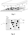
- FIG. 1 we see in perspective view a photosensitive set which is symbolized by an MTR matrix of N lines and P columns of pixels, ie NxP pixels.
- the matrix is illuminated uniformly by a source of illumination LS.
- Objects OBJ to count are posed on the matrix. They hide the pixels on which they rest, that is to say that the Source light LS does not reach these pixels. The other pixels are illuminated by the source.
- the objects are represented as having a parallelepipedal shape of the same dimensions as the pixels, each object completely covering a pixel and only one.
- this identity of form and dimensions between the pixel and the object to be counted is not absolutely obligatory, provided that we know the surface covered by an object to count.
- the surface of a pixel gives the resolution with which one can detect the surfaces of objects posed on the matrix: the smaller it is, the better one can count small objects and the more the account of the larger objects is precise.
- the surface covered by an object can thus cover several pixels of the matrix.
- the light source preferably comprises a diffusing plate similar to the light box of a liquid crystal display.
- This plate preferably has the same surface as the matrix.
- the photosensitive matrix is a large passive matrix. Typically it comprises a sandwich structure comprising a substrate sheet, preferably of flexible plastic material, coated with a photoconductive material, preferably organic and deposited by a printing method, between a network of rear-facing conductors and a network of conductors. front side.
- the front face conductors are preferably transparent (indium tin oxide ITO) or must be very narrow so as not to overly obscure the photosensitive material; backplane drivers do not need to be transparent.
- Backplane drivers can be line drivers and front-panel drivers can be column drivers, or the opposite. If all the line conductors are simultaneously powered by the same potential, they can be combined into a single overall conductive layer occupying most of the surface of the sheet.
- a portion of photoconductive material at the intersection of a line conductor and a column conductor defines a photosensitive pixel and behaves like a photoresistor or preferably a photodiode connected between the line conductor and the line conductor. column.
- the line conductor is powered by a bias voltage and the column conductor is connected to a read circuit associated with the column.
- the read circuit reads the current of each column, that is to say the sum of the currents of the photodiodes which are connected to this column conductor and which are further polarized by the bias voltage.
- Each photodiode which is polarized by a line conductor indeed leaves to the column conductor a current which depends on the illumination of this photodiode.
- the figure 2 is a simplified representation, seen from above, of the matrix of pixels in which the white squares represent pixels illuminated by the uniform source and the black squares represent pixels masked by an object covering the pixel and having the same dimensions as the pixel.
- a shaded square on which we will return later represents a pixel masked by an opaque layer.
- This square has an elementary surface S E. It is in relation to this surface that we define the surface of an object placed.
- the figure 3 is a representation of the same matrix, in the form of a passive matrix array of photodiodes in which the cathodes of the photodiodes of the same line are connected to the same line conductor and the anodes of the same column are all connected to one same column driver respectively.
- Each photodiode at the intersection of a line conductor and a column conductor represents a pixel of the MTR matrix.
- the bias voltage Vpol is applied to all line conductors together, and the read circuit is brought to a potential more negative than the voltage Vpol so as to polarize the photodiodes in reverse.
- the potentials and the directions of the photodiodes could be reversed, the photodiodes being always reverse biased so that the current supplied by the photodiode to a column conductor is always a photodiode reverse bias current, this current depending on the illumination.
- Illuminated photodiodes are shown in white. Unlighted photodiodes, because hidden by an object, are shown in black.
- the number of objects placed on each column is determined from a calculation of the number of pixels of a column that are not illuminated by the source because they are masked by an object. This calculation is done by measuring the current I M produced by the column.
- the number of illuminated pixels is Nn, when the number of masked pixels is n.
- two matrix reference columns are used, one (CrefA) having one or more artificially masked pixels, for example a local opaque layer, the other (CrefB) having no masked pixels, or a layer opaque or by an object. It is forbidden to deposit an object to count on these reference columns.
- the difference between the current I refB of the CrefB column and the current I refA of the CrefA column represents the average current I E provided by a pixel. If k pixels (k> 1) are masked in the CrefA column, divide by k the difference of the CrefB and CrefA column currents to obtain the average current I E.
- the number n i of pixels masked in a column of rank i is obtained by dividing by I E the difference between the current I refB of the column and the current I mi measured by the reading circuit of the column of rank i).
- This difference measurement suppresses the contribution of the dark current of the photodiodes, assuming that this current is approximately uniform for all the photodiodes of the matrix.
- the fully illuminated column current can be used to determine the average illumination of the supposedly uniformly illuminated matrix. It can be used for purposes of servoing the light source. It could also be used, if divided by the number N of pixels in the column, to determine the average current I E of a pixel, but it is preferable to determine this current by difference between the currents of the reference columns CrefA and CrefB, in order to suppress the contribution of the dark current and the time drifts of the response of the photodiodes and / or lighting.
- the first CrefA reference column comprises N-1 masked pixels, for example by an opaque layer deposited on its surface, and a single illuminated pixel; the second reference column CrefB contains all the N pixels masked by an opaque layer.
- the difference between the currents of the CrefA column and CrefB column directly gives the elementary current I E of an illuminated pixel.
- the currents of the other columns are divided by I E to have the number of illuminated pixels; the complement to N gives the number of hidden pixels in the column.
- the effects of a non-uniformity of illumination can be compensated by duplicating the reference columns, for example by placing a pair of reference columns CrefA, CrefB to the left of the matrix, and another pair , CrefA ', CrefB', to the right of the matrix as represented by figure 5 .
- the results of the two columns are averaged to obtain the elementary current I E.
- the read circuits are current reading circuits, the current delivered by the reverse biased photodiodes being a good representation of the illumination. But the currents can be converted into voltage so that they can be more easily converted by an analog-to-digital converter (not shown) in order to calculate the number of objects laid.
- a particularly interesting solution for the measurement of the current and the voltage conversion is to use the current of a reference column and copy it in the other reference columns to apply to each reading circuit associated with a column not the current of this column but the difference between the current of this column and the current of the reference column.
- the figure 6 represents such an embodiment, in which the reference column which serves to establish the current to be copied is a CrefA column of which all the pixels are illuminated.
- the corresponding column conductor is connected to the drain of a diode-connected reference transistor Tref, the gate of which is connected to the drain and whose source is at a ground potential.
- a reading circuit associated with this column other than this transistor which receives the entire current of the CrefA column.
- the current in this transistor is equal to NI E if the N pixels of the reference column are fully illuminated.
- This current is copied by a respective copy transistor of each reading circuit associated with a column.
- the copy transistor has its source connected to ground and its gate connected to the gate of the first transistor.
- the drain of the copy transistor is not connected to its gate; it is connected to the column conductor corresponding to this read circuit and is also connected to an inverting input of an operational amplifier.
- the non-inverting input of the amplifier is connected to the gate of the reference transistor and therefore to the gates of the feedback transistors. This configuration allows a reliable copy of the current by polarizing each drain to the gate voltage of the reference transistor by the feedback action of the operational amplifier.
- the operational amplifier is looped back between its output and its inverting input by a resistance of value R (the same value for all the circuits).
- the number n i is obtained by the ratio of these voltages V i and V E.
- the voltages can be converted by an analog-to-digital converter (not shown) to then allow easy digital division.
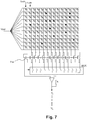
- the individual read circuit for determining the number of masked pixels in a column is individual for each column. However, for reasons of space, it may be preferable to temporally multiplex the reading by directing the currents coming from each column successively to a single common current-voltage conversion circuit comprising, for example, the operational amplifier and the resistance of the figure 6 . The output voltages are then read successively and not simultaneously.
- the multiplexer MUX may be placed downstream of the copy transistors of the N-1 columns other than the CrefA column, as shown in FIG. figure 7 ; the reading circuit associated with a column then comprises the copying transistor and the switch of the multiplexer, and the amplifier and the resistance are shared between all the read circuits.
- the multiplexer MUX can also be placed upstream, and in this case there is only one feedback transistor, placed between the output of the multiplexer and the input of the amplifier, as shown in FIG. figure 8 .
- a capacitance can be paralleled to the amplifier loopback resistor to filter transitions during multiplexer switching.
- the column conductors are connected directly to a multiplexer.
- the multiplexer successively selects each column under the control of a simple shift register, and it then directs this stream and it alone to a single read circuit.
- the first reference column is first selected, then the second; the reference current is calculated by difference. Then the other columns are selected one after the other for a direct measurement of their current.
- the principle described above makes it possible to determine the number of objects placed in each column of the matrix. It is therefore possible to draw a histogram per column, that is to say a curve whose abscissa is the number of the column and the ordinate is the number of objects placed in the column.
- the figure 9 schematically represents the result of this histogram calculation.
- the elementary surface that defines the resolution of the measurement is equal to the width of the column multiplied by a fraction of the height of the column.
- the reference column CrefB which will be used to determine the elementary current must therefore be masked on this column surface fraction, as indicated by the hatched surface of the column. figure 11 .
- the other CrefA reference column is fully lit and no objects are lying on it.
- the difference in the measurements of the reference columns determines the elementary current I E which would be generated by the hatched fraction alone if it were lighted. This fraction preferably corresponds to the surface of an object to be detected, as in the case of the preceding figures.
- the currents generated in the presence of the laid objects are then measured globally or column by column and compared with the reference current to calculate column by column or globally the number of elementary surfaces masked.
- the difference from the previous figures is only the fact that the photodiodes are not subdivided into several pixels in the direction of the height.
- the figure 12 represents the three steps of this measurement.
- the first step (12a) gives a current measurement I when the entire photodiode is illuminated;
- the second step (12b) is made by masking an elementary surface that can be located anywhere in the photodiode, here for example in the center; it gives a current II E ;
- the third step (12c) gives a current In.I E , where n is the number of objects to count, expressed as a multiple of the elementary surface masked at the second step.
- n is the number of objects to count, expressed as a multiple of the elementary surface masked at the second step.
- the figure 13 represents the case of a single large photodiode, on which the objects are placed without concern of their position; it is clear that we can still count the objects: there is no change from the figure 11 which represented the objects posed according to a precise matrix organization.
- n i which may not be integers but rather fractional; these fractional values are added to obtain the best possible approximation for the total number of objects placed on the matrix.
- the figure 14 represents a matrix on which the objects are rotated or shifted relative to the columns of pixels (and possibly to the lines, but the lines do not matter if the reading is done in column).
- the surface of the sheet must be broken down into sufficiently small elementary surfaces.
- the limit is given by the noise: it is necessary that the total noise, classical quadratic sum of thermal noise, noise "shot” (also called Schottky noise or photonic noise) and noise in 1 / f remains below of the current generated by the illumination of an elementary surface by the light source LS.
- integrating amplifier capacitor transimpedance amplifier
Landscapes
- Physics & Mathematics (AREA)
- General Physics & Mathematics (AREA)
- Engineering & Computer Science (AREA)
- Theoretical Computer Science (AREA)
- Transforming Light Signals Into Electric Signals (AREA)
- Photometry And Measurement Of Optical Pulse Characteristics (AREA)
- Length Measuring Devices By Optical Means (AREA)
Claims (12)
- Verfahren zur Zählung von Objekten, dadurch gekennzeichnet, dass:- man eine lichtempfindliche Anordnung (MTR) verwendet, welche mindestens ein lichtleitendes Element und eine einheitliche Beleuchtungsquelle (LS) zum Beleuchten der lichtempfindlichen Anordnung beinhaltet,- man eine Stromreferenz (IE) bestimmt, welche durch die lichtempfindliche Anordnung für einen beleuchteten Bereich dieser Anordnung bereitgestellt wird, welcher einer Elementaroberfläche (SE) entspricht, welche ein bestimmter Bruchteil der Oberfläche der lichtempfindlichen Anordnung ist,- man die zu zählenden Objekte (OBJ) an der lichtempfindlichen Anordnung anordnet, man die lichtempfindliche Anordnung durch die Quelle beleuchtet, wobei die aufgestellten Objekte einen Teil der Oberfläche der lichtempfindlichen Anordnung verdecken,- man den von der Anordnung bereitgestellten Strom (IM) misst, und man die durch die Objekte verdeckte Oberfläche und anschließend die Anzahl der Objekte anhand des gemessenen Stroms und der Stromreferenz bestimmt.
- Verfahren nach Anspruch 1, dadurch gekennzeichnet, dass die lichtempfindliche Anordnung aus einem flexiblen Blatt besteht, welches mit einem gedruckten, organischen, lichtleitenden Material und mit Leitern beschichtet ist, welche es ermöglichen, einen auf die Beleuchtung zurückzuführenden Strom aufzunehmen.
- Verfahren nach einem der Ansprüche 1 und 2, dadurch gekennzeichnet, dass die lichtempfindliche Anordnung eine passive Matrix aus N Zeilen und P Spalten (wobei N und P Ganzzahlen größer als oder gleich 1 sind) von lichtleitenden Elementen beinhaltet, welche jeweils am Schnittpunkt zwischen einem Zeilenleiter und einem Spaltenleiter der Matrix befindlich sind.
- Verfahren nach Anspruch 3, dadurch gekennzeichnet, dass die Matrix mindestens eine Referenzspalte beinhaltet, welche eine bekannte Anzahl k (wobei k eine Ganzzahl oder gleich null ist) von nicht beleuchteten Elementaroberflächen besitzt, wobei diese Spalte zum Bestimmen des Referenzstroms dient, welcher der Beleuchtung einer einzigen Elementaroberfläche entspricht.
- Verfahren nach Anspruch 4, dadurch gekennzeichnet, dass die Matrix mindestens eine andere Referenzspalte beinhaltet, welche k' (wobei k' sich von k unterscheidet) nicht beleuchtete Elementaroberflächen beinhaltet und man die Differenz der Ströme beider Referenzspalten misst, um davon den durch die Beleuchtung einer einzigen Elementaroberfläche erzeugten Strom abzuleiten.
- Verfahren nach einem der Ansprüche 4 und 5, dadurch gekennzeichnet, dass die Referenzspalten dupliziert sind und die von zwei duplizierten Spalten bereitgestellten Ströme gemittelt sind.
- Verfahren nach einem der Ansprüche 3 bis 6, dadurch gekennzeichnet, dass ein Leseschaltkreis mit jeder Spalte verbunden ist, und dieser Schaltkreis differenziell ist, wobei der Schaltkreis die Differenz zwischen dem durch eine Referenzspalte, deren sämtliche Pixel beleuchtet sind, oder deren sämtliche Pixel verdeckt sind, bereitgestellten Strom und dem von der mit dem Leseschaltkreis verbundenen Spalte bereitgestellten Strom misst.
- Verfahren nach Anspruch 7, dadurch gekennzeichnet, dass die Matrix eine einzige Zeile mit lichtleitenden Elementen länglicher Form besitzt, wobei die Elementaroberfläche einen Anteil der Höhe eines lichtleitenden Elements darstellt.
- Verfahren nach einem der vorhergehenden Ansprüche, dadurch gekennzeichnet, dass die Leseschaltkreise mit jeder Spalte, aber auch mit jeder Zeile der Matrix verbunden sind.
- Verfahren nach einem der Ansprüche 1 bis 3, dadurch gekennzeichnet, dass die lichtempfindliche Anordnung nicht in mehrere lichtleitende Elemente unterteilt ist, welche individuell oder spaltenweise gelesen werden können, sondern aus einem einzigen lichtleitenden Element besteht, dessen global durch die Beleuchtung erzeugten Strom man liest.
- Verfahren nach einem der Ansprüche 1 bis 10, dadurch gekennzeichnet, dass die lichtleitenden Elemente Photodioden sind.
- Vorrichtung zur Zählung von Objekten, welche eine passive Matrix aus N Zeilen und P Spalten (wobei N und P Ganzzahlen gleich oder größer als 1 sind) von lichtleitenden Elementen, an welcher man Objekte platzieren kann, um die Matrix teilweise zu verdecken, eine einheitliche Lichtquelle, welche die gesamte Matrix beleuchtet, Mittel zum Bestimmen eines Elementarstroms, welcher der Beleuchtung einer Elementaroberfläche entspricht, welche ein Bruchteil der Oberfläche der Matrix ist, Mittel zum Messen mindestens eines durch die Matrix im Beisein von Objekten abgegebenen Stroms, welche die Matrix teilweise verdecken, und Mittel zum Bestimmen der durch die Objekte verdeckten Oberfläche und anschließend der Anzahl der Objekte, anhand des abgegebenen Stroms und des Elementarstroms, beinhaltet.
Applications Claiming Priority (2)
| Application Number | Priority Date | Filing Date | Title |
|---|---|---|---|
| FR1252025A FR2987922B1 (fr) | 2012-03-06 | 2012-03-06 | Procede et dispositif de comptage d'objets |
| PCT/EP2013/053417 WO2013131750A1 (fr) | 2012-03-06 | 2013-02-21 | Procede et dispositif de comptage d'objets |
Publications (2)
| Publication Number | Publication Date |
|---|---|
| EP2823441A1 EP2823441A1 (de) | 2015-01-14 |
| EP2823441B1 true EP2823441B1 (de) | 2019-06-12 |
Family
ID=47891605
Family Applications (1)
| Application Number | Title | Priority Date | Filing Date |
|---|---|---|---|
| EP13709788.7A Active EP2823441B1 (de) | 2012-03-06 | 2013-02-21 | Verfahren und vorrichtung zur zählung von objekten |
Country Status (6)
| Country | Link |
|---|---|
| US (1) | US9817027B2 (de) |
| EP (1) | EP2823441B1 (de) |
| JP (1) | JP6289383B2 (de) |
| KR (1) | KR102060213B1 (de) |
| FR (1) | FR2987922B1 (de) |
| WO (1) | WO2013131750A1 (de) |
Families Citing this family (6)
| Publication number | Priority date | Publication date | Assignee | Title |
|---|---|---|---|---|
| US20140152801A1 (en) | 2009-10-28 | 2014-06-05 | Alentic Microscience Inc. | Detecting and Using Light Representative of a Sample |
| WO2011053631A1 (en) | 2009-10-28 | 2011-05-05 | Alentic Microscience Inc. | Microscopy imaging |
| US9075225B2 (en) | 2009-10-28 | 2015-07-07 | Alentic Microscience Inc. | Microscopy imaging |
| US9518920B2 (en) | 2013-06-26 | 2016-12-13 | Alentic Microscience Inc. | Sample processing improvements for microscopy |
| US10502666B2 (en) | 2013-02-06 | 2019-12-10 | Alentic Microscience Inc. | Sample processing improvements for quantitative microscopy |
| US10508898B2 (en) | 2017-03-23 | 2019-12-17 | Hitachi, Ltd. | Interference measurement device having a variable phase element |
Family Cites Families (15)
| Publication number | Priority date | Publication date | Assignee | Title |
|---|---|---|---|---|
| US3493772A (en) * | 1967-05-29 | 1970-02-03 | Palo Alto Medical Research Fou | Bacterial counting machine and method |
| US4139766A (en) * | 1977-08-15 | 1979-02-13 | Sunkist Growers, Inc. | Apparatus and method for counting fruits and other objects |
| DE3419883A1 (de) * | 1984-05-28 | 1985-11-28 | Amazonen Werke Dreyer H | Verfahren und vorrichtung zum optischen zaehlen kleiner koerperchen |
| US5076692A (en) * | 1990-05-31 | 1991-12-31 | Tencor Instruments | Particle detection on a patterned or bare wafer surface |
| US5218211A (en) * | 1991-10-23 | 1993-06-08 | The United States Of America As Represented By The Secretary Of Commerce | System for sampling the sizes, geometrical distribution, and frequency of small particles accumulating on a solid surface |
| EP0698084B1 (de) * | 1993-05-14 | 1998-06-24 | Minnesota Mining And Manufacturing Company | Verfahren zur schnellen quantifizierung von microorganismenwachstum |
| US5504573A (en) * | 1993-10-13 | 1996-04-02 | Man-Gill Chemical Company | Apparatus and method for analyzing particles deposited on a substrate using substantially continuous profile data |
| US5457312A (en) * | 1994-08-24 | 1995-10-10 | Ford Motor Company | Method and apparatus for counting flat sheets of specularly reflective material |
| US6836527B1 (en) * | 2004-02-06 | 2004-12-28 | Batching Systems, Inc. | Method and apparatus for detecting and counting articles |
| US7129465B2 (en) * | 2004-04-13 | 2006-10-31 | The United States Of America As Represented By The Secretary Of The Army | Electronically code-multiplexed readout of photo-detector arrays |
| US7570786B2 (en) * | 2004-08-30 | 2009-08-04 | Antoun Ateya | Automatic digital object counting and verification system and associated method |
| JP4922938B2 (ja) * | 2005-08-31 | 2012-04-25 | アグロシステム株式会社 | 集卵コンベアによって移送される卵をカウントするための卵カウンタ |
| JP4511442B2 (ja) * | 2005-09-30 | 2010-07-28 | 富士フイルム株式会社 | 感度可変型撮像素子及びこれを搭載した撮像装置 |
| JP2009031097A (ja) | 2007-07-26 | 2009-02-12 | Canon Inc | 微粒子を用いた測定対象物質の定量・検出方法及びその方法に用いる測定装置 |
| AU2012389816A1 (en) * | 2012-09-13 | 2015-04-02 | Halliburton Energy Services, Inc. | Spatial heterodyne integrated computational element (SH-ICE) spectrometer |
-
2012
- 2012-03-06 FR FR1252025A patent/FR2987922B1/fr not_active Expired - Fee Related
-
2013
- 2013-02-21 KR KR1020147027881A patent/KR102060213B1/ko active IP Right Grant
- 2013-02-21 JP JP2014560297A patent/JP6289383B2/ja not_active Expired - Fee Related
- 2013-02-21 WO PCT/EP2013/053417 patent/WO2013131750A1/fr active Application Filing
- 2013-02-21 EP EP13709788.7A patent/EP2823441B1/de active Active
- 2013-02-21 US US14/383,456 patent/US9817027B2/en not_active Expired - Fee Related
Non-Patent Citations (1)
| Title |
|---|
| None * |
Also Published As
| Publication number | Publication date |
|---|---|
| KR20140146602A (ko) | 2014-12-26 |
| WO2013131750A1 (fr) | 2013-09-12 |
| US9817027B2 (en) | 2017-11-14 |
| JP2015515051A (ja) | 2015-05-21 |
| US20150035516A1 (en) | 2015-02-05 |
| KR102060213B1 (ko) | 2019-12-27 |
| FR2987922A1 (fr) | 2013-09-13 |
| JP6289383B2 (ja) | 2018-03-07 |
| FR2987922B1 (fr) | 2014-04-18 |
| EP2823441A1 (de) | 2015-01-14 |
Similar Documents
| Publication | Publication Date | Title |
|---|---|---|
| EP2823441B1 (de) | Verfahren und vorrichtung zur zählung von objekten | |
| CA2632505C (fr) | Dispositif de detection de rayonnement infrarouge a detecteurs bolometriques | |
| EP0362352B1 (de) | Belegleser | |
| EP0245147A1 (de) | Röntgen-Bilderfassungstafel und deren Herstellungsverfahren | |
| FR2613567A1 (fr) | Dispositif detecteur photosensible pour systemes electroniques de prise d'images en couleur | |
| FR2971879A1 (fr) | Dispositif d'affichage avec cellules photovoltaiques integrees, a luminosite amelioree | |
| FR2988862A1 (fr) | Procede et dispositif de localisation d'un objet magnetique | |
| CA2826150A1 (fr) | Dispositif d'affichage avec cellules photovoltaiques integrees, a luminosite amelioree | |
| FR2627923A1 (fr) | Matrice d'elements photosensibles et detecteur de radiations comportant une telle matrice, notamment detecteur de rayons x a double energie | |
| EP3210162A1 (de) | Vorrichtung zur erfassung digitaler fingerabdrücke | |
| EP3384256B1 (de) | Verfahren zur erfassung eines wärmemusters | |
| EP0055966A2 (de) | Matrixanzeigevorrichtung mit zwei Arten von Linienelektroden und Verfahren zu ihrer Ansteuerung | |
| EP2378258A1 (de) | Detektor für elektromagnetische Strahlung eine reduzierte Empfindlichkeit gegen räumliches Rauschen aufweisend | |
| FR2988872A1 (fr) | Ecran avec localisation d'objet magnetique | |
| EP1354360B1 (de) | Photoelektrisches element mit sehr grossem dynamikbereich | |
| EP2914952A1 (de) | Vorrichtung zur aufnahme eines bildes einer probe mit einer anlage zur regelung der erwärmung einer halterung zur aufnahme der probe und zugehöriges bildgebungssystem | |
| FR2919962A1 (fr) | Procede de correction de sensibilite et capteur d'image matriciel pour la mise en oeuvre de ce procede | |
| EP2553623A1 (de) | Analoger elektronischer schaltkreis zur verarbeitung eines lichtsignals sowie entsprechendes verarbeitungssystem und -verfahren | |
| EP0965224A1 (de) | Verfahren zur steuerung einer lichtempfindlichen vorrichtung mit schwacher remanenz und lichtempfindliche vorrichtung zur durchführung des verfahrens | |
| EP3394792A1 (de) | Oled-beleuchteter drucksensor | |
| EP4123281A1 (de) | Matrixdrucksensor mit neuronalem netzwerk und entsprechendes kalibrierungsverfahren | |
| EP3767260A1 (de) | Sensor und verfahren zur erfassung eines wärmemusters mit doppelter integration | |
| WO2016027028A1 (fr) | Dispositif d'acquisition d'empreintes digitales | |
| FR2744547A1 (fr) | Procede et systeme de detection de la presence et d'identification d'objets ou de personnes dans un volume donne, notamment le passager dans un vehicule automobile | |
| FR3046276A1 (fr) | Procede pour obtenir une image fusionnee d'une empreinte papillaire |
Legal Events
| Date | Code | Title | Description |
|---|---|---|---|
| PUAI | Public reference made under article 153(3) epc to a published international application that has entered the european phase |
Free format text: ORIGINAL CODE: 0009012 |
|
| 17P | Request for examination filed |
Effective date: 20140902 |
|
| AK | Designated contracting states |
Kind code of ref document: A1 Designated state(s): AL AT BE BG CH CY CZ DE DK EE ES FI FR GB GR HR HU IE IS IT LI LT LU LV MC MK MT NL NO PL PT RO RS SE SI SK SM TR |
|
| AX | Request for extension of the european patent |
Extension state: BA ME |
|
| DAX | Request for extension of the european patent (deleted) | ||
| GRAP | Despatch of communication of intention to grant a patent |
Free format text: ORIGINAL CODE: EPIDOSNIGR1 |
|
| STAA | Information on the status of an ep patent application or granted ep patent |
Free format text: STATUS: GRANT OF PATENT IS INTENDED |
|
| INTG | Intention to grant announced |
Effective date: 20190204 |
|
| GRAS | Grant fee paid |
Free format text: ORIGINAL CODE: EPIDOSNIGR3 |
|
| GRAA | (expected) grant |
Free format text: ORIGINAL CODE: 0009210 |
|
| STAA | Information on the status of an ep patent application or granted ep patent |
Free format text: STATUS: THE PATENT HAS BEEN GRANTED |
|
| AK | Designated contracting states |
Kind code of ref document: B1 Designated state(s): AL AT BE BG CH CY CZ DE DK EE ES FI FR GB GR HR HU IE IS IT LI LT LU LV MC MK MT NL NO PL PT RO RS SE SI SK SM TR |
|
| REG | Reference to a national code |
Ref country code: GB Ref legal event code: FG4D Free format text: NOT ENGLISH |
|
| REG | Reference to a national code |
Ref country code: CH Ref legal event code: EP |
|
| REG | Reference to a national code |
Ref country code: AT Ref legal event code: REF Ref document number: 1143537 Country of ref document: AT Kind code of ref document: T Effective date: 20190615 |
|
| REG | Reference to a national code |
Ref country code: IE Ref legal event code: FG4D Free format text: LANGUAGE OF EP DOCUMENT: FRENCH |
|
| REG | Reference to a national code |
Ref country code: DE Ref legal event code: R096 Ref document number: 602013056477 Country of ref document: DE |
|
| REG | Reference to a national code |
Ref country code: NL Ref legal event code: MP Effective date: 20190612 |
|
| REG | Reference to a national code |
Ref country code: LT Ref legal event code: MG4D |
|
| PG25 | Lapsed in a contracting state [announced via postgrant information from national office to epo] |
Ref country code: HR Free format text: LAPSE BECAUSE OF FAILURE TO SUBMIT A TRANSLATION OF THE DESCRIPTION OR TO PAY THE FEE WITHIN THE PRESCRIBED TIME-LIMIT Effective date: 20190612 Ref country code: LT Free format text: LAPSE BECAUSE OF FAILURE TO SUBMIT A TRANSLATION OF THE DESCRIPTION OR TO PAY THE FEE WITHIN THE PRESCRIBED TIME-LIMIT Effective date: 20190612 Ref country code: FI Free format text: LAPSE BECAUSE OF FAILURE TO SUBMIT A TRANSLATION OF THE DESCRIPTION OR TO PAY THE FEE WITHIN THE PRESCRIBED TIME-LIMIT Effective date: 20190612 Ref country code: NO Free format text: LAPSE BECAUSE OF FAILURE TO SUBMIT A TRANSLATION OF THE DESCRIPTION OR TO PAY THE FEE WITHIN THE PRESCRIBED TIME-LIMIT Effective date: 20190912 Ref country code: SE Free format text: LAPSE BECAUSE OF FAILURE TO SUBMIT A TRANSLATION OF THE DESCRIPTION OR TO PAY THE FEE WITHIN THE PRESCRIBED TIME-LIMIT Effective date: 20190612 Ref country code: AL Free format text: LAPSE BECAUSE OF FAILURE TO SUBMIT A TRANSLATION OF THE DESCRIPTION OR TO PAY THE FEE WITHIN THE PRESCRIBED TIME-LIMIT Effective date: 20190612 |
|
| PG25 | Lapsed in a contracting state [announced via postgrant information from national office to epo] |
Ref country code: BG Free format text: LAPSE BECAUSE OF FAILURE TO SUBMIT A TRANSLATION OF THE DESCRIPTION OR TO PAY THE FEE WITHIN THE PRESCRIBED TIME-LIMIT Effective date: 20190912 Ref country code: RS Free format text: LAPSE BECAUSE OF FAILURE TO SUBMIT A TRANSLATION OF THE DESCRIPTION OR TO PAY THE FEE WITHIN THE PRESCRIBED TIME-LIMIT Effective date: 20190612 Ref country code: LV Free format text: LAPSE BECAUSE OF FAILURE TO SUBMIT A TRANSLATION OF THE DESCRIPTION OR TO PAY THE FEE WITHIN THE PRESCRIBED TIME-LIMIT Effective date: 20190612 Ref country code: GR Free format text: LAPSE BECAUSE OF FAILURE TO SUBMIT A TRANSLATION OF THE DESCRIPTION OR TO PAY THE FEE WITHIN THE PRESCRIBED TIME-LIMIT Effective date: 20190913 |
|
| REG | Reference to a national code |
Ref country code: AT Ref legal event code: MK05 Ref document number: 1143537 Country of ref document: AT Kind code of ref document: T Effective date: 20190612 |
|
| PG25 | Lapsed in a contracting state [announced via postgrant information from national office to epo] |
Ref country code: EE Free format text: LAPSE BECAUSE OF FAILURE TO SUBMIT A TRANSLATION OF THE DESCRIPTION OR TO PAY THE FEE WITHIN THE PRESCRIBED TIME-LIMIT Effective date: 20190612 Ref country code: SK Free format text: LAPSE BECAUSE OF FAILURE TO SUBMIT A TRANSLATION OF THE DESCRIPTION OR TO PAY THE FEE WITHIN THE PRESCRIBED TIME-LIMIT Effective date: 20190612 Ref country code: AT Free format text: LAPSE BECAUSE OF FAILURE TO SUBMIT A TRANSLATION OF THE DESCRIPTION OR TO PAY THE FEE WITHIN THE PRESCRIBED TIME-LIMIT Effective date: 20190612 Ref country code: PT Free format text: LAPSE BECAUSE OF FAILURE TO SUBMIT A TRANSLATION OF THE DESCRIPTION OR TO PAY THE FEE WITHIN THE PRESCRIBED TIME-LIMIT Effective date: 20191014 Ref country code: CZ Free format text: LAPSE BECAUSE OF FAILURE TO SUBMIT A TRANSLATION OF THE DESCRIPTION OR TO PAY THE FEE WITHIN THE PRESCRIBED TIME-LIMIT Effective date: 20190612 Ref country code: RO Free format text: LAPSE BECAUSE OF FAILURE TO SUBMIT A TRANSLATION OF THE DESCRIPTION OR TO PAY THE FEE WITHIN THE PRESCRIBED TIME-LIMIT Effective date: 20190612 Ref country code: NL Free format text: LAPSE BECAUSE OF FAILURE TO SUBMIT A TRANSLATION OF THE DESCRIPTION OR TO PAY THE FEE WITHIN THE PRESCRIBED TIME-LIMIT Effective date: 20190612 |
|
| PG25 | Lapsed in a contracting state [announced via postgrant information from national office to epo] |
Ref country code: SM Free format text: LAPSE BECAUSE OF FAILURE TO SUBMIT A TRANSLATION OF THE DESCRIPTION OR TO PAY THE FEE WITHIN THE PRESCRIBED TIME-LIMIT Effective date: 20190612 Ref country code: IS Free format text: LAPSE BECAUSE OF FAILURE TO SUBMIT A TRANSLATION OF THE DESCRIPTION OR TO PAY THE FEE WITHIN THE PRESCRIBED TIME-LIMIT Effective date: 20191012 Ref country code: IT Free format text: LAPSE BECAUSE OF FAILURE TO SUBMIT A TRANSLATION OF THE DESCRIPTION OR TO PAY THE FEE WITHIN THE PRESCRIBED TIME-LIMIT Effective date: 20190612 Ref country code: ES Free format text: LAPSE BECAUSE OF FAILURE TO SUBMIT A TRANSLATION OF THE DESCRIPTION OR TO PAY THE FEE WITHIN THE PRESCRIBED TIME-LIMIT Effective date: 20190612 |
|
| REG | Reference to a national code |
Ref country code: DE Ref legal event code: R097 Ref document number: 602013056477 Country of ref document: DE |
|
| PG25 | Lapsed in a contracting state [announced via postgrant information from national office to epo] |
Ref country code: TR Free format text: LAPSE BECAUSE OF FAILURE TO SUBMIT A TRANSLATION OF THE DESCRIPTION OR TO PAY THE FEE WITHIN THE PRESCRIBED TIME-LIMIT Effective date: 20190612 |
|
| PLBE | No opposition filed within time limit |
Free format text: ORIGINAL CODE: 0009261 |
|
| STAA | Information on the status of an ep patent application or granted ep patent |
Free format text: STATUS: NO OPPOSITION FILED WITHIN TIME LIMIT |
|
| PG25 | Lapsed in a contracting state [announced via postgrant information from national office to epo] |
Ref country code: DK Free format text: LAPSE BECAUSE OF FAILURE TO SUBMIT A TRANSLATION OF THE DESCRIPTION OR TO PAY THE FEE WITHIN THE PRESCRIBED TIME-LIMIT Effective date: 20190612 Ref country code: PL Free format text: LAPSE BECAUSE OF FAILURE TO SUBMIT A TRANSLATION OF THE DESCRIPTION OR TO PAY THE FEE WITHIN THE PRESCRIBED TIME-LIMIT Effective date: 20190612 |
|
| 26N | No opposition filed |
Effective date: 20200313 |
|
| PG25 | Lapsed in a contracting state [announced via postgrant information from national office to epo] |
Ref country code: SI Free format text: LAPSE BECAUSE OF FAILURE TO SUBMIT A TRANSLATION OF THE DESCRIPTION OR TO PAY THE FEE WITHIN THE PRESCRIBED TIME-LIMIT Effective date: 20190612 Ref country code: IS Free format text: LAPSE BECAUSE OF FAILURE TO SUBMIT A TRANSLATION OF THE DESCRIPTION OR TO PAY THE FEE WITHIN THE PRESCRIBED TIME-LIMIT Effective date: 20200224 |
|
| PG2D | Information on lapse in contracting state deleted |
Ref country code: IS |
|
| REG | Reference to a national code |
Ref country code: CH Ref legal event code: PL |
|
| REG | Reference to a national code |
Ref country code: BE Ref legal event code: MM Effective date: 20200229 |
|
| PG25 | Lapsed in a contracting state [announced via postgrant information from national office to epo] |
Ref country code: LU Free format text: LAPSE BECAUSE OF NON-PAYMENT OF DUE FEES Effective date: 20200221 Ref country code: MC Free format text: LAPSE BECAUSE OF FAILURE TO SUBMIT A TRANSLATION OF THE DESCRIPTION OR TO PAY THE FEE WITHIN THE PRESCRIBED TIME-LIMIT Effective date: 20190612 |
|
| PG25 | Lapsed in a contracting state [announced via postgrant information from national office to epo] |
Ref country code: CH Free format text: LAPSE BECAUSE OF NON-PAYMENT OF DUE FEES Effective date: 20200229 Ref country code: LI Free format text: LAPSE BECAUSE OF NON-PAYMENT OF DUE FEES Effective date: 20200229 |
|
| PG25 | Lapsed in a contracting state [announced via postgrant information from national office to epo] |
Ref country code: IE Free format text: LAPSE BECAUSE OF NON-PAYMENT OF DUE FEES Effective date: 20200221 |
|
| PG25 | Lapsed in a contracting state [announced via postgrant information from national office to epo] |
Ref country code: BE Free format text: LAPSE BECAUSE OF NON-PAYMENT OF DUE FEES Effective date: 20200229 |
|
| PGFP | Annual fee paid to national office [announced via postgrant information from national office to epo] |
Ref country code: FR Payment date: 20210226 Year of fee payment: 9 |
|
| PGFP | Annual fee paid to national office [announced via postgrant information from national office to epo] |
Ref country code: GB Payment date: 20210216 Year of fee payment: 9 Ref country code: DE Payment date: 20210209 Year of fee payment: 9 |
|
| PG25 | Lapsed in a contracting state [announced via postgrant information from national office to epo] |
Ref country code: MT Free format text: LAPSE BECAUSE OF FAILURE TO SUBMIT A TRANSLATION OF THE DESCRIPTION OR TO PAY THE FEE WITHIN THE PRESCRIBED TIME-LIMIT Effective date: 20190612 Ref country code: CY Free format text: LAPSE BECAUSE OF FAILURE TO SUBMIT A TRANSLATION OF THE DESCRIPTION OR TO PAY THE FEE WITHIN THE PRESCRIBED TIME-LIMIT Effective date: 20190612 |
|
| PG25 | Lapsed in a contracting state [announced via postgrant information from national office to epo] |
Ref country code: MK Free format text: LAPSE BECAUSE OF FAILURE TO SUBMIT A TRANSLATION OF THE DESCRIPTION OR TO PAY THE FEE WITHIN THE PRESCRIBED TIME-LIMIT Effective date: 20190612 |
|
| REG | Reference to a national code |
Ref country code: DE Ref legal event code: R119 Ref document number: 602013056477 Country of ref document: DE |
|
| GBPC | Gb: european patent ceased through non-payment of renewal fee |
Effective date: 20220221 |
|
| PG25 | Lapsed in a contracting state [announced via postgrant information from national office to epo] |
Ref country code: FR Free format text: LAPSE BECAUSE OF NON-PAYMENT OF DUE FEES Effective date: 20220228 |
|
| PG25 | Lapsed in a contracting state [announced via postgrant information from national office to epo] |
Ref country code: GB Free format text: LAPSE BECAUSE OF NON-PAYMENT OF DUE FEES Effective date: 20220221 Ref country code: DE Free format text: LAPSE BECAUSE OF NON-PAYMENT OF DUE FEES Effective date: 20220901 |