EP2823290B1 - System and process for measuring strain in materials at high spatial resolution - Google Patents
System and process for measuring strain in materials at high spatial resolution Download PDFInfo
- Publication number
- EP2823290B1 EP2823290B1 EP13757134.5A EP13757134A EP2823290B1 EP 2823290 B1 EP2823290 B1 EP 2823290B1 EP 13757134 A EP13757134 A EP 13757134A EP 2823290 B1 EP2823290 B1 EP 2823290B1
- Authority
- EP
- European Patent Office
- Prior art keywords
- pattern
- diffraction
- sample
- strain
- diffraction pattern
- Prior art date
- Legal status (The legal status is an assumption and is not a legal conclusion. Google has not performed a legal analysis and makes no representation as to the accuracy of the status listed.)
- Active
Links
Images
Classifications
-
- G—PHYSICS
- G01—MEASURING; TESTING
- G01N—INVESTIGATING OR ANALYSING MATERIALS BY DETERMINING THEIR CHEMICAL OR PHYSICAL PROPERTIES
- G01N23/00—Investigating or analysing materials by the use of wave or particle radiation, e.g. X-rays or neutrons, not covered by groups G01N3/00 – G01N17/00, G01N21/00 or G01N22/00
- G01N23/22—Investigating or analysing materials by the use of wave or particle radiation, e.g. X-rays or neutrons, not covered by groups G01N3/00 – G01N17/00, G01N21/00 or G01N22/00 by measuring secondary emission from the material
- G01N23/225—Investigating or analysing materials by the use of wave or particle radiation, e.g. X-rays or neutrons, not covered by groups G01N3/00 – G01N17/00, G01N21/00 or G01N22/00 by measuring secondary emission from the material using electron or ion
- G01N23/2251—Investigating or analysing materials by the use of wave or particle radiation, e.g. X-rays or neutrons, not covered by groups G01N3/00 – G01N17/00, G01N21/00 or G01N22/00 by measuring secondary emission from the material using electron or ion using incident electron beams, e.g. scanning electron microscopy [SEM]
-
- H—ELECTRICITY
- H01—ELECTRIC ELEMENTS
- H01J—ELECTRIC DISCHARGE TUBES OR DISCHARGE LAMPS
- H01J37/00—Discharge tubes with provision for introducing objects or material to be exposed to the discharge, e.g. for the purpose of examination or processing thereof
- H01J37/26—Electron or ion microscopes; Electron or ion diffraction tubes
-
- G—PHYSICS
- G01—MEASURING; TESTING
- G01N—INVESTIGATING OR ANALYSING MATERIALS BY DETERMINING THEIR CHEMICAL OR PHYSICAL PROPERTIES
- G01N23/00—Investigating or analysing materials by the use of wave or particle radiation, e.g. X-rays or neutrons, not covered by groups G01N3/00 – G01N17/00, G01N21/00 or G01N22/00
- G01N23/20—Investigating or analysing materials by the use of wave or particle radiation, e.g. X-rays or neutrons, not covered by groups G01N3/00 – G01N17/00, G01N21/00 or G01N22/00 by using diffraction of the radiation by the materials, e.g. for investigating crystal structure; by using scattering of the radiation by the materials, e.g. for investigating non-crystalline materials; by using reflection of the radiation by the materials
- G01N23/20058—Measuring diffraction of electrons, e.g. low energy electron diffraction [LEED] method or reflection high energy electron diffraction [RHEED] method
-
- G—PHYSICS
- G01—MEASURING; TESTING
- G01N—INVESTIGATING OR ANALYSING MATERIALS BY DETERMINING THEIR CHEMICAL OR PHYSICAL PROPERTIES
- G01N3/00—Investigating strength properties of solid materials by application of mechanical stress
- G01N3/02—Details
-
- H—ELECTRICITY
- H01—ELECTRIC ELEMENTS
- H01J—ELECTRIC DISCHARGE TUBES OR DISCHARGE LAMPS
- H01J37/00—Discharge tubes with provision for introducing objects or material to be exposed to the discharge, e.g. for the purpose of examination or processing thereof
- H01J37/26—Electron or ion microscopes; Electron or ion diffraction tubes
- H01J37/261—Details
-
- H—ELECTRICITY
- H01—ELECTRIC ELEMENTS
- H01J—ELECTRIC DISCHARGE TUBES OR DISCHARGE LAMPS
- H01J37/00—Discharge tubes with provision for introducing objects or material to be exposed to the discharge, e.g. for the purpose of examination or processing thereof
- H01J37/26—Electron or ion microscopes; Electron or ion diffraction tubes
- H01J37/295—Electron or ion diffraction tubes
- H01J37/2955—Electron or ion diffraction tubes using scanning ray
-
- H—ELECTRICITY
- H01—ELECTRIC ELEMENTS
- H01J—ELECTRIC DISCHARGE TUBES OR DISCHARGE LAMPS
- H01J2237/00—Discharge tubes exposing object to beam, e.g. for analysis treatment, etching, imaging
- H01J2237/15—Means for deflecting or directing discharge
-
- H—ELECTRICITY
- H01—ELECTRIC ELEMENTS
- H01J—ELECTRIC DISCHARGE TUBES OR DISCHARGE LAMPS
- H01J2237/00—Discharge tubes exposing object to beam, e.g. for analysis treatment, etching, imaging
- H01J2237/244—Detection characterized by the detecting means
- H01J2237/2448—Secondary particle detectors
-
- H—ELECTRICITY
- H01—ELECTRIC ELEMENTS
- H01J—ELECTRIC DISCHARGE TUBES OR DISCHARGE LAMPS
- H01J2237/00—Discharge tubes exposing object to beam, e.g. for analysis treatment, etching, imaging
- H01J2237/245—Detection characterised by the variable being measured
- H01J2237/24571—Measurements of non-electric or non-magnetic variables
- H01J2237/24585—Other variables, e.g. energy, mass, velocity, time, temperature
-
- H—ELECTRICITY
- H01—ELECTRIC ELEMENTS
- H01J—ELECTRIC DISCHARGE TUBES OR DISCHARGE LAMPS
- H01J2237/00—Discharge tubes exposing object to beam, e.g. for analysis treatment, etching, imaging
- H01J2237/26—Electron or ion microscopes
- H01J2237/2602—Details
-
- H—ELECTRICITY
- H01—ELECTRIC ELEMENTS
- H01J—ELECTRIC DISCHARGE TUBES OR DISCHARGE LAMPS
- H01J2237/00—Discharge tubes exposing object to beam, e.g. for analysis treatment, etching, imaging
- H01J2237/26—Electron or ion microscopes
- H01J2237/28—Scanning microscopes
- H01J2237/2802—Transmission microscopes
Definitions
- the invention in general relates to a system and process for electron microscopy to determine the local strain in materials, and in particular to precession electron diffraction and the generation of position-resolved strain distributions from samples subjected to electron microscopy.
- NBD patterns have been used in the past to measure strain in crystalline samples. See, e.g., Koji Usuda et al., Strain characterization in SOI and strained-Si on SGOI MOSFET channel using nano-beam electron diffraction (NBD), Materials Science and Engineering: B, Volumes 124-125, 5 December 2005, Pages 143-147 .
- the absolute strain is derived from the measured shift in position of one or more spots in the electron diffraction pattern from the strained crystal relative to the position of the same spots in the electron diffraction pattern from an unstrained crystal.
- Either manual measurement or semi-automated measurement using image/feature registration techniques have been used to measure the shift in the diffraction spots. But those methods suffer from some significant systematic errors that result from strong changes in the beam intensity distribution that are not due to strain (see the description of dynamical diffraction below). The precision required for some measurements, which can be less than 0.1% strain, is often not attainable with those methods.
- the present invention has utility as a system and a process of performing PED in TEM.
- a TEM with an accelerating voltage between 20 kV and 1.5 MV is fitted with a device (the "Precession Device") that applies signals to the TEM that produce a time-dependent change in the angle of the incident electron beam.
- the Precession Device also applies signals to the TEM to stop the motion of the diffraction patterns that is induced by the change of angle of the incident electron beam.
- the incident electron beam is a small diameter probe that produces NBD patterns and raster scanned (“STEM”) images.
- the TEM is also fitted in specific embodiments with a camera (the "Camera”) to record TEM images and/or diffraction patterns.
- a TEM 101 has an attached Precession Device 112 and Camera 109.
- the Precession Device 112 generates beam coil control electrical signals 110 that control the beam deflection coils 102, which in turn control the angle and the position of the electron beam or probe 104 incident on the sample 105.
- the Precession Device 112 also generates image deflection coil electrical signals 111 that control the image deflection coils 103, which in turn compensate for the effect of the incident beam tilt and shift on the transmitted beam 106.
- the Precession Device generates incident beam tilts according to various cyclic tilt protocols, at characteristic tilt angles of typically 0.1 to 2 degrees, and at frequencies of typically 10-1000 Hz.
- the image compensation signals 111 are adjusted so the diffraction pattern 108 remains at a fixed position while the incident beam is tilted according to its defined protocol.
- the Software positions the incident electron beam in patterns as described above. At each position of the incident beam, the Software acquires and stores an Unknown Pattern and an X-ray spectrum and/or EELS spectrum from that position of the sample. A Measured Strain is calculated from each of the Unknown Patterns using the Fitting Algorithm, and an elemental composition is calculated from each of the X-ray spectra and/or EELS spectra.
- the Software constructs a Strain Distribution, and also spatially registered elemental composition distributions ("Composition Distributions").
- a process is provided in which at each position of the incident beam, the Software acquires and stores an Unknown Pattern and an X-ray spectrum and/or EELS spectrum from that position of the sample.
- a Measured Strain is calculated from each of the Unknown Patterns and an elemental composition is calculated from each of the X-ray spectra and/or EELS spectra.
- Such X-ray and EELS spectra may be acquired with any precession angle from 0 degrees (no precession) up to a specific precession angle (up to about 2 degrees) where the X-ray and EELS signal may be enhanced.
- strain may affect the intensity, shape, or position of features in the EELS spectra. If these changes are correlated with the strain measured from the diffraction patterns, the features in the EELS spectra may be used as another measure of the strain in the sample.
Landscapes
- Chemical & Material Sciences (AREA)
- Analytical Chemistry (AREA)
- Physics & Mathematics (AREA)
- Health & Medical Sciences (AREA)
- Life Sciences & Earth Sciences (AREA)
- Biochemistry (AREA)
- General Health & Medical Sciences (AREA)
- General Physics & Mathematics (AREA)
- Immunology (AREA)
- Pathology (AREA)
- Crystallography & Structural Chemistry (AREA)
- Analysing Materials By The Use Of Radiation (AREA)
- Length-Measuring Devices Using Wave Or Particle Radiation (AREA)
Description
- The application claims priority benefit of United States Provisional Application Serial Number
61/608,413 filed 8 March 2013 - The invention in general relates to a system and process for electron microscopy to determine the local strain in materials, and in particular to precession electron diffraction and the generation of position-resolved strain distributions from samples subjected to electron microscopy.
- Electron diffraction patterns offer the ability to measure the lattice parameters of crystalline materials. A small (< 10 nanometer (nm)) focused electron probe can be produced by a transmission electron microscope ("TEM"), and the probe can be positioned in two dimensions to a precision of better than 1 nm. The probe is amenable to being moved quickly (< 1 ms) to any position over a large (> 1 µm) field of view. For electron-transparent samples, it is therefore possible to produce so-called nanobeam diffraction ("NBD") patterns from many discrete points in a sample.
- NBD patterns have been used in the past to measure strain in crystalline samples. See, e.g., Koji Usuda et al., Strain characterization in SOI and strained-Si on SGOI MOSFET channel using nano-beam electron diffraction (NBD), Materials Science and Engineering: B, Volumes 124-125, 5 December 2005, Pages 143-147. The absolute strain is derived from the measured shift in position of one or more spots in the electron diffraction pattern from the strained crystal relative to the position of the same spots in the electron diffraction pattern from an unstrained crystal. Either manual measurement or semi-automated measurement using image/feature registration techniques have been used to measure the shift in the diffraction spots. But those methods suffer from some significant systematic errors that result from strong changes in the beam intensity distribution that are not due to strain (see the description of dynamical diffraction below). The precision required for some measurements, which can be less than 0.1% strain, is often not attainable with those methods.
- The accuracy and precision of the strain measurement can be improved by fitting an entire diffraction pattern from a strained sample with another diffraction pattern from an unstrained sample that is distorted in directions corresponding to the strain vectors. By fitting the entire diffraction pattern instead of just individual spots, the accuracy and precision are improved over the measurement by including the physical constraint that the shifts of higher-index spots in one direction are linearly proportional to the shifts of their lower-index relatives. The stochastic uncertainly is also reduced by fitting all of the diffraction spots, as opposed to only measuring the limited number of spots whose intensity distribution is not changed too much by dynamical diffraction.
- The main systematic errors in measuring spot positions from conventional NBD patterns, and therefore in calculating strain within a material, arise from the fact that the diffraction spot intensities and centers of mass are strongly affected by dynamical electron diffraction. A shift in center of mass of a diffraction spot leads to an error in measuring the spot shift, and the variation in spot intensities can lead to errors in fitting a complete diffraction pattern. The dynamical diffraction effect is strongly influenced by the relative beam/crystal orientation and by sample thickness. Relative orientation variations occur because of sample bending, which is common for thin TEM samples, while local variations in sample thickness are virtually unavoidable using common TEM sample preparation techniques.
- Precession electron diffraction ("PED") has been used to reduce the negative effects of dynamical diffraction. See, e.g., R. Vincent, P.A. Midgley, Double conical beam-rocking system for measurement of integrated electron diffraction intensities, Ultramicroscopy, Volume 53, Issue 3, March 1994, Pages 271-282. In PED, the incident electron beam is precessed at a relatively high frequency (10-1000 Hz) through a small (0.2-5 degrees) angle. This precession reduces the visible effects of dynamical diffraction, so that the diffraction patterns are influenced minimally by variations in sample thickness and bending. Additionally, many additional higher-order reflections appear, which are more sensitive to strain than the lower-order reflections, further enhancing the precision of the strain measurement.
- Thus, there exists a need for a process for measuring strain in materials with improved precision. There further exists a need for performing such measurements with high spatial resolution to allow other details of a sampled field to be correlated with strain values derived from the same sample area.
- A process and a system for measuring strain according to claims 1 and 13, respectively, are provided. Preferred embodiments are set out in the dependent claims.
-
-
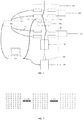
FIG. 1 is a diagram showing the major components of the present invention, along with a ray path of the electrons as they pass through the device. -
FIG. 2 is a depiction of the variation of the distortion parameter σ of the Distorted Pattern (open circles) that leads to a best match with the Undistorted Pattern (solid circles). -
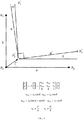
FIG. 3 is a depiction of the geometry of the affine transformation, along with the equations for the affine transformation and the relationship of the affine coefficients to the geometry. - The present invention has utility as a system and a process of performing PED in TEM. In one embodiment of the present invention, a TEM with an accelerating voltage between 20 kV and 1.5 MV is fitted with a device (the "Precession Device") that applies signals to the TEM that produce a time-dependent change in the angle of the incident electron beam. The Precession Device also applies signals to the TEM to stop the motion of the diffraction patterns that is induced by the change of angle of the incident electron beam. In specific embodiments, the incident electron beam is a small diameter probe that produces NBD patterns and raster scanned ("STEM") images. The TEM is also fitted in specific embodiments with a camera (the "Camera") to record TEM images and/or diffraction patterns. A computer, through software running on the computer (the "Software"), controls various operational aspects of the TEM, the Precession Device, and the Camera. The Software acquires PED patterns using the Camera, and can cause the position of the electron beam on the sample to change in a controlled manner.
- PED patterns from a TEM sample are acquired using the Software from areas of unknown strain ("Unknown Pattern"). A PED pattern ("Reference Pattern") is either acquired using the Software from a TEM sample of known strain, or is calculated using the Software from a kinematical or dynamical diffraction theoretical model. It should be appreciated that calculated kinematical patterns are computationally more tractable than dynamical patterns, and also that diffraction patterns acquired with precession are a good representation of kinematical patterns, even for thicker samples. The Reference Pattern is acquired or calculated from a sample with the same crystalline structure and the same relative electron beam/sample orientation as from the Unknown Pattern. The Software uses a numerical image warping algorithm (see for example Wolberg, G. (1990), Digital Image Warping, IEEE Computer Society Press) to create a distorted version ("Distorted Pattern") of either the Reference Pattern or the Unknown Pattern, leaving the other pattern ("Undistorted Pattern") undistorted. The distortion will minimally include normal expansion or contraction and shear distortion in one or more directions in addition to rotation and translation. The magnitude of each distortion is described by a Distortion Coefficient. The Software determines the set of Distortion Coefficients that produces the best match of the Distorted Pattern to the Undistorted Pattern. From the Distortion Coefficients that produce the best match, the Software calculates the value of the unknown strain relative to the known strain.
- The present invention also has application in instances when the Software acquires Unknown Patterns from arrays of positions on the sample. Each of the Unknown Patterns is processed as described above, and the calculated strains are assembled in the Software as one- or two-dimensional strain distributions.
- According to the present invention, a TEM is also in certain embodiments fitted with an energy-dispersive X-ray ("EDX") detector that detects X-rays coming from the sample in the area illuminated by the electron beam and/or an electron energy loss spectroscopy ("EELS") detector which determines the energy losses of the electrons that have gone through the illuminated area of the sample. The Software or other software acquires spectra from the EDX and EELS detectors from the same positions as the PED patterns, and can derive compositional information that is spatially registered with strain information for the TEM sample.
- With reference to
FIG. 1 , a TEM 101 has an attachedPrecession Device 112 andCamera 109. ThePrecession Device 112 generates beam coil controlelectrical signals 110 that control thebeam deflection coils 102, which in turn control the angle and the position of the electron beam orprobe 104 incident on thesample 105. ThePrecession Device 112 also generates image deflection coilelectrical signals 111 that control theimage deflection coils 103, which in turn compensate for the effect of the incident beam tilt and shift on the transmittedbeam 106. The Precession Device generates incident beam tilts according to various cyclic tilt protocols, at characteristic tilt angles of typically 0.1 to 2 degrees, and at frequencies of typically 10-1000 Hz. Theimage compensation signals 111 are adjusted so thediffraction pattern 108 remains at a fixed position while the incident beam is tilted according to its defined protocol. - A
sample 105 is placed in a TEM as a specimen to be measured and is tilted to an orientation such that adiffraction pattern 108 is observed containing diffraction spots corresponding to the lattice directions in which the strain is to be measured. It is appreciated that the specific orientation of thesample 105 is immaterial to the inventive process. The characteristic tilt angle of the tilt protocol is adjusted so that minimal dynamical diffraction effects are observed. This minimal dynamical diffraction effect adjustment can be observed by changing the position of the incident electron beam, and when dynamical diffraction effects are minimal, there will be only minor changes in the observed diffraction patterns as the incident beam is moved. Theelectron beam 104 is then positioned on an area of thesample 105 of unknown strain, and one or more Unknown Patterns are acquired from theCamera 109 and are stored using the Software. The frequency of the tilt protocol is set such that the tilt protocol cycles an integral number of times during the Camera exposure. In one embodiment, theelectron beam 104 is positioned on an area of thesample 105 of known (ideally zero) strain, and one or more Reference Patterns are acquired from theCamera 109 and are stored using the Software. In another embodiment, a Reference Pattern is calculated using the Software or using other software. In yet another embodiment, a Reference Pattern is recalled from a database of electron diffraction patterns using the Software. It is appreciated that additional spatial information can be obtained from asample 105 through collection of TEM camera images or STEM images in order to locate specific areas for measuring strain. It should also be appreciated that a representative diffractogram is also readily obtained through Fourier transform of a TEM or STEM lattice image of thesample 105. - In some embodiments to the present invention, the
sample 105 is held within a straining TEM specimen holder or anvil holder to induce dynamic strain or deformation of a sample with patterns collected as a function of forces applied to thesample 105. It is appreciated that such holders are also available with thermal and tilt control of thesample 105. - One of either the Unknown Pattern or the Reference Pattern is numerically distorted by the Software in one or more directions with normal, shear, rotational and translational distortions. In one embodiment, the Distorted Pattern is distorted using an affine transformation of all pixels of the image, where the coefficients of the affine transformation are the Distortion Coefficients. Such a distortion can lead to some corresponding distortion of the shape of the diffraction spots. In another embodiment, each diffraction spot of the Distorted Pattern is individually extracted and translated by a vector calculated from an affine transformation and distortion coefficients are the coefficients of the affine transformation. Such a distortion will maintain the shape of the diffraction spots.
FIG. 2 shows an example of such a distortion, where the affine transformation includes only a scale factor σ in the x-direction.FIG. 3 shows the geometry and the functional form of the affine transformation. The normal strain components εxx and εyy are equal to 1/sx and 1/sy , respectively, in the case that the Reference Pattern is distorted. The Distortion Coefficients (in this case the affine coefficients) are adjusted by the Software to produce a best match of the Distorted Pattern to the Undistorted Pattern. In specific embodiments, the best match is determined by Levenberg-Marquardt non-linear fitting, non-linear least squares regression, or by Gauss-Newton or other known regression algorithms. In still other embodiments, the best match is determined by maximizing the image cross correlation coefficient using a Quasi-Newton, other linear optimization algorithm, or simplex algorithm that varies the Distortion Coefficients. - It is appreciated that in other inventive aspects, the Software controls the position of the incident beam on the sample. Various patterns of incident beam positions are produced on the sample, including but not limited to multiple points along a curve, and two-dimensional grids of points within an area. At each position of the incident beam, the Software acquires and stores an Unknown Pattern from that position of the sample. A Measured Strain is calculated from each of the Unknown Patterns using the Fitting Algorithm, and the Software constructs a spatial distribution of strain (a "Strain Distribution"). It is appreciated that the diffraction pattern used for comparison can be a measured pattern, a calculated pattern, a library reference, or a combination thereof. A library of reference patterns is readily assembled by a standards generating facility or through contribution of patterns by a community of users.
- Repetition of the inventive process is also used to generate a spatial map of the strain distributions across the sample through collection of diffraction patterns from different regions of the sample. Such topographical strain mapping is amenable to overlaying with spatially correlated chemical compositional information derived from the EDX and/or EELS detectors, or structural features obtained from TEM or STEM images, or a combination thereof.
- It is appreciated that in other inventive aspects, an energy-
dispersive X-ray detector 107 and/orEELS detector 114 is also mounted on the TEM. The Software acquires X-ray spectra from the EDX detector or EELS data from the EELS detector. Optionally, the EDX or EELS data is collected at the same position on the sample where the Software acquires PED patterns from the Camera. The Software analyzes the additional EDX or EELS data to determine the local elemental composition of the sample at the location of the incident beam, in addition to the measured strain at that location. - It is appreciated that in other inventive aspects, the Software positions the incident electron beam in patterns as described above. At each position of the incident beam, the Software acquires and stores an Unknown Pattern and an X-ray spectrum and/or EELS spectrum from that position of the sample. A Measured Strain is calculated from each of the Unknown Patterns using the Fitting Algorithm, and an elemental composition is calculated from each of the X-ray spectra and/or EELS spectra. The Software constructs a Strain Distribution, and also spatially registered elemental composition distributions ("Composition Distributions").
- In certain embodiments of the present invention where an EELS detector is present, a process is provided in which at each position of the incident beam, the Software acquires and stores an Unknown Pattern and an X-ray spectrum and/or EELS spectrum from that position of the sample. A Measured Strain is calculated from each of the Unknown Patterns and an elemental composition is calculated from each of the X-ray spectra and/or EELS spectra. Such X-ray and EELS spectra may be acquired with any precession angle from 0 degrees (no precession) up to a specific precession angle (up to about 2 degrees) where the X-ray and EELS signal may be enhanced. (S.Estrade'et al., EELS signal enhancement by means of beam precession in the TEM,Ultramicroscopy (2012)). In addition to the compositional information in the EELS spectra, strain may affect the intensity, shape, or position of features in the EELS spectra. If these changes are correlated with the strain measured from the diffraction patterns, the features in the EELS spectra may be used as another measure of the strain in the sample.
- Patent documents and publications mentioned in the specification are indicative of the levels of those skilled in the art to which the invention pertains.
- The foregoing description is illustrative of particular embodiments of the invention, but is not meant to be a limitation upon the practice thereof. The following claims are intended to define the scope of the invention.
Claims (15)
- A process for measuring strain in a crystalline material comprising:placing a sample (105) of the material into a transmission electron microscope (101) as a specimen; andenergizing the transmission electron microscope to create an electron beam (104) with an incident angle to the material; andgenerating electrical beam deflection coil control signals (110) that control a plurality of beam deflection coils (102) of the transmission electron microscope so as to control the angle and position of the electron beam incident on the sample, thereby generating incident beam tilts according to a cyclic tilt protocol; andgenerating electrical image deflection coil control signals (111) that control a plurality of image deflection coils (103) of the transmission electron microscope;viewing a first diffraction pattern (108) from the material with dynamical diffraction effects;adjusting at least one of the beam deflection coil control signals (110) to reduce the dynamical diffraction effects;adjusting at least one of the image deflection coil control signals (111) to stop the motion of the diffraction pattern induced by the beam deflection coil control signals (110);collecting after the last adjusting step a second diffraction pattern from an area of the material with known strain; and collecting a third diffraction pattern from an area of the material with unknown strain.
- The process of claim 1, wherein the beam deflection coil control signals modify the incident angle between 0.1 and 2 degrees or change the beam incident angle in a cyclic time-dependent manner at a frequency of between 10-1000 Hz, or wherein the dynamical diffraction effect is observed by changing the position of the beam and is minimized when only minor changes are noted in the first diffraction pattern as the incident beam position is changed.
- The process of claim 1 wherein the second diffraction pattern is collected with a camera (109), calculated using kinematical electron diffraction theory or recovered from a stored file.
- The process of any one of claims 1-3 further comprising collecting the third diffraction pattern with a camera.
- The process of any one of claims 1-3 further comprising:collecting the third diffraction pattern with a camera and using an image warping algorithm with one or more distortion coefficients to create a distorted pattern of either the second or third diffraction pattern, and leaving the other diffraction pattern undistorted; orcollecting the third diffraction pattern with a camera and using an image warping algorithm with one or more distortion coefficients to create a distorted pattern of either the second or third diffraction pattern, and leaving the other diffraction pattern undistorted, wherein the image warping algorithm is an affine transformation and the distortion coefficients are the coefficients of the affine transformation.
- The process of claim 5, further comprising measuring the quality of the match between the distorted pattern and the undistorted pattern, or comprising measuring the quality of the match between the distorted pattern and the undistorted pattern and finding the distortion coefficients that produce the highest quality match between the distorted pattern and the undistorted pattern.
- The process of claim 6 further comprising determining the measured strain in one or more directions in the sample from the values of the distortion coefficients.
- The process of claim 7, wherein the algorithm for finding the best match is a nonlinear least squares fitting algorithm to fit the distorted pattern to the undistorted pattern, where the fitting parameters for the algorithm are the distortion coefficients, or
wherein the quality of the match is defined by the image cross correlation coefficient between the undistorted pattern and the distorted pattern, and the algorithm for finding the highest quality match is a linear optimization algorithm to find the maximum value of the cross correlation coefficient, where the input values for the optimization algorithm are the distortion coefficients. - The process of claim 8 further comprising collecting a plurality of third diffraction patterns from different positions on the sample.
- The process of claim 9 further comprising measuring the strain from the diffraction patterns at each position on the sample, or
measuring the strain from the diffraction patterns at each position on the sample and creating one or more maps of the strain distributions across the sample. - The process of claim 8 further comprising measuring a chemical composition of the material, or
measuring a chemical composition of the material at the position where the third diffraction pattern was acquired, or
measuring a chemical composition of the material by energy dispersive X-ray spectroscopy and/or electron energy loss spectroscopy. - The process of claim 10, further comprising measuring the chemical composition of the material at each position where a diffraction pattern was acquired, or
measuring the chemical composition of the material at each position where a diffraction pattern was acquired by energy dispersive X-ray spectroscopy and/or electron energy loss spectroscopy, or
measuring the chemical composition of the material at each position where a diffraction pattern was acquired by energy dispersive X-ray spectroscopy and/or electron energy loss spectroscopy and creating one or more maps of the chemical composition distribution across the sample. - A system for measuring strain in a material comprising:a transmission electron microscope (101) having beam deflection coils (102) and image deflection coils (103), a stage for receiving a sample (105) of the material, and generating an electron beam upon being energized, the electron beam (104) having an incident angle to the sample;a precession device (112) configured to generate electrical beam deflection coil control signals (110) that control the beam deflection coils (102) so as to control the angle and position of the electron beam incident on the sample, thereby generating incident beam tilts according to a cyclic tilt protocol, and electrical image deflection coil control signals (111) that control the image deflection coils (103); andsoftware configured to control the beam deflection coil control signals (110) and the image deflection coil control signals (111) to collect non-moving diffraction patterns (108) from the sample with reduced dynamical diffraction effects, in which at least one of the beam deflection control signals are adjusted to reduce dynamical diffraction effects and at least one of the image deflection control signals are adjusted to stop the motion of the diffraction pattern induced by the beam deflection control signals;characterized in that the software is further configured tocollect, after the last adjusting step, a non-moving diffraction pattern from an area of the material of known strain;collect a further non-moving diffraction pattern from at least one area of the material with unknown strain; anddetermine the strain in the material.
- The system of claim 13, further comprising a camera (109) positioned for collecting the diffraction patterns from the material, or wherein the incident angle of the beam is changed by the precession device between 0.1 and 2 degrees or wherein the incident angle is changed in a cyclic time-dependent manner with a cyclic frequency of 10-1000 Hz.
- The system of claims 13 or 14, further comprising an energy dispersive X-ray detector (107) and software for acquiring spectra from the X-ray detector to determine the composition of the material, or
an electron energy loss spectrometer (114) and software for acquiring spectra from the electron energy loss spectrometer to determine the composition of the material.
Applications Claiming Priority (2)
| Application Number | Priority Date | Filing Date | Title |
|---|---|---|---|
| US201261608413P | 2012-03-08 | 2012-03-08 | |
| PCT/US2013/029947 WO2013134680A1 (en) | 2012-03-08 | 2013-03-08 | System and process for measuring strain in materials at high spatial resolution |
Publications (3)
| Publication Number | Publication Date |
|---|---|
| EP2823290A1 EP2823290A1 (en) | 2015-01-14 |
| EP2823290A4 EP2823290A4 (en) | 2015-11-18 |
| EP2823290B1 true EP2823290B1 (en) | 2017-09-13 |
Family
ID=49117394
Family Applications (1)
| Application Number | Title | Priority Date | Filing Date |
|---|---|---|---|
| EP13757134.5A Active EP2823290B1 (en) | 2012-03-08 | 2013-03-08 | System and process for measuring strain in materials at high spatial resolution |
Country Status (6)
| Country | Link |
|---|---|
| US (1) | US9274070B2 (en) |
| EP (1) | EP2823290B1 (en) |
| JP (1) | JP6116598B2 (en) |
| KR (1) | KR101999988B1 (en) |
| CN (1) | CN104272096B (en) |
| WO (1) | WO2013134680A1 (en) |
Families Citing this family (16)
| Publication number | Priority date | Publication date | Assignee | Title |
|---|---|---|---|---|
| EP2642279B1 (en) * | 2012-03-19 | 2015-07-01 | Universidad de Barcelona | Method and system for improving characteristic peak signals in analytical electron microscopy |
| US9601308B2 (en) * | 2012-10-31 | 2017-03-21 | Hitachi, Ltd. | Spectroscopic element and charged particle beam device using the same |
| WO2014190239A1 (en) * | 2013-05-24 | 2014-11-27 | Drexel University | Strain mapping in tem using precession electron diffraction |
| US9279777B2 (en) * | 2013-08-06 | 2016-03-08 | International Business Machines Corporation | Analyzing strain distribution in semiconductor structures using nano-beam diffraction |
| SG10201401046UA (en) | 2014-03-27 | 2015-10-29 | Nanyang Polytechnic | Real-time multi-point diffraction-based imaging system for strain measurement |
| WO2016174707A1 (en) * | 2015-04-27 | 2016-11-03 | 株式会社日立ハイテクノロジーズ | Charged particle beam device and sample observation method using same device |
| TWI656339B (en) * | 2015-10-30 | 2019-04-11 | 聯華電子股份有限公司 | Method for analyzing strain of semiconductor channel |
| US9978560B2 (en) | 2016-06-30 | 2018-05-22 | International Business Machines Corporation | System and method for performing nano beam diffraction analysis |
| KR102512987B1 (en) | 2016-07-08 | 2023-03-22 | 삼성전자주식회사 | method of analyzing lattice strain of semiconductor device |
| FR3055969B1 (en) | 2016-09-14 | 2020-02-07 | Commissariat A L'energie Atomique Et Aux Energies Alternatives | METHOD FOR DETERMINING THE DEFLECTION OF AN ELECTRON BEAM RESULTING FROM AN ELECTRIC FIELD AND / OR A MAGNETIC FIELD |
| EP3379236B1 (en) * | 2017-03-20 | 2019-09-11 | TESCAN Brno, s.r.o. | Scanning transmission electron microscope |
| FR3074949B1 (en) | 2017-12-11 | 2019-12-20 | Electricite De France | METHOD, DEVICE AND PROGRAM FOR PROCESSING DIFFRACTION IMAGES OF CRYSTALLINE MATERIAL |
| FR3098641B1 (en) * | 2019-07-08 | 2021-07-23 | Commissariat Energie Atomique | Analysis method by electron microscopy |
| CN113806760B (en) * | 2021-04-09 | 2024-05-17 | 京东科技控股股份有限公司 | Method, device, electronic equipment and storage medium for acquiring correlation coefficient between features |
| CN114964590B (en) * | 2022-05-26 | 2023-08-18 | 中国工程物理研究院核物理与化学研究所 | Electron microscopic analysis method for tritide nano-scale micro-region stress distribution |
| US20250076038A1 (en) * | 2023-08-30 | 2025-03-06 | Fei Company | Fast and accurate strain mapping using electron diffraction |
Family Cites Families (14)
| Publication number | Priority date | Publication date | Assignee | Title |
|---|---|---|---|---|
| JP3134853B2 (en) * | 1998-08-21 | 2001-02-13 | 日本電気株式会社 | Crystal distortion measuring method, crystal distortion measuring device and recording medium |
| EP1365229B1 (en) | 2001-02-28 | 2012-12-12 | Hitachi, Ltd. | Electron nano diffraction method of measuring strain and stress by detecting one or a plurality of diffraction spots |
| JP3867524B2 (en) * | 2001-07-05 | 2007-01-10 | 株式会社日立製作所 | Observation apparatus and observation method using electron beam |
| JP3888980B2 (en) * | 2003-03-18 | 2007-03-07 | 株式会社日立ハイテクノロジーズ | Material identification system |
| US7601956B2 (en) * | 2003-09-02 | 2009-10-13 | Avilov Anatoly Sergeevich | Method for measuring diffraction patterns from a transmission electron microscopy to determine crystal structures and a device therefor |
| JP2005032732A (en) * | 2004-09-15 | 2005-02-03 | Hitachi Ltd | Scanning electron microscope |
| JP4262184B2 (en) | 2004-10-12 | 2009-05-13 | 株式会社日立ハイテクノロジーズ | Transmission electron microscope and image observation method using the same |
| JP2007173132A (en) | 2005-12-26 | 2007-07-05 | Hitachi High-Technologies Corp | Scanning transmission electron microscope and method for adjusting scanning transmission electron microscope |
| CN101206185A (en) * | 2007-10-23 | 2008-06-25 | 湘潭大学 | A Method for Measuring Residual Stress of Ferroelectric Film |
| EP2818852B1 (en) | 2008-11-06 | 2019-01-02 | Nanomegas SPRL | Methods and devices for high throughput crystal structure analysis by electron diffraction |
| EP2197018A1 (en) | 2008-12-12 | 2010-06-16 | FEI Company | Method for determining distortions in a particle-optical apparatus |
| JP5160520B2 (en) | 2009-09-25 | 2013-03-13 | 株式会社東芝 | Crystal lattice moire pattern acquisition method and scanning microscope |
| JP5517584B2 (en) * | 2009-12-08 | 2014-06-11 | 株式会社日立ハイテクノロジーズ | electronic microscope |
| EP2413345B1 (en) * | 2010-07-29 | 2013-02-20 | Carl Zeiss NTS GmbH | Charged particle beam system |
-
2013
- 2013-03-08 CN CN201380024099.2A patent/CN104272096B/en active Active
- 2013-03-08 EP EP13757134.5A patent/EP2823290B1/en active Active
- 2013-03-08 KR KR1020147028408A patent/KR101999988B1/en active Active
- 2013-03-08 US US14/383,713 patent/US9274070B2/en active Active
- 2013-03-08 WO PCT/US2013/029947 patent/WO2013134680A1/en not_active Ceased
- 2013-03-08 JP JP2014561154A patent/JP6116598B2/en active Active
Non-Patent Citations (1)
| Title |
|---|
| None * |
Also Published As
| Publication number | Publication date |
|---|---|
| JP6116598B2 (en) | 2017-04-19 |
| KR101999988B1 (en) | 2019-07-15 |
| EP2823290A1 (en) | 2015-01-14 |
| WO2013134680A1 (en) | 2013-09-12 |
| EP2823290A4 (en) | 2015-11-18 |
| US20150076346A1 (en) | 2015-03-19 |
| CN104272096B (en) | 2016-12-14 |
| CN104272096A (en) | 2015-01-07 |
| KR20140143178A (en) | 2014-12-15 |
| US9274070B2 (en) | 2016-03-01 |
| JP2015514974A (en) | 2015-05-21 |
Similar Documents
| Publication | Publication Date | Title |
|---|---|---|
| US9274070B2 (en) | System and process for measuring strain in materials at high spatial resolution | |
| Kammers et al. | Digital image correlation under scanning electron microscopy: methodology and validation | |
| EP1274114B1 (en) | Observation apparatus using an electron beam | |
| Chen et al. | Quantitative atomic resolution elemental mapping via absolute-scale energy dispersive X-ray spectroscopy | |
| US7633064B2 (en) | Electric charged particle beam microscopy and electric charged particle beam microscope | |
| Yuan et al. | Lattice strain mapping using circular Hough transform for electron diffraction disk detection | |
| Lee et al. | Electron dose dependence of signal-to-noise ratio, atom contrast and resolution in transmission electron microscope images | |
| EP1365229B1 (en) | Electron nano diffraction method of measuring strain and stress by detecting one or a plurality of diffraction spots | |
| JP7228558B2 (en) | Method for improving transmission Kikuchi diffraction patterns | |
| EP2966668B1 (en) | Method of calibrating a scanning transmission charged-particle microscope | |
| Berkels et al. | Joint non-rigid image registration and reconstruction for quantitative atomic resolution scanning transmission electron microscopy | |
| Kimoto et al. | Spatially resolved diffractometry with atomic-column resolution | |
| JP5431169B2 (en) | Electron microscope and method for measuring defocus deviation or resolution limit | |
| Koster et al. | Measurement of the spherical aberration coefficient of transmission electron microscopes by beam-tilt-induced image displacements | |
| WO2015037313A1 (en) | Scanning transmission electron microscope and aberration measurement method therefor | |
| Willhammar et al. | 3D reconstruction of atomic structures from high angle annular dark field (HAADF) STEM images and its application on zeolite silicalite-1 | |
| Dycus et al. | Influence of experimental conditions on atom column visibility in energy dispersive X-ray spectroscopy | |
| JP5777984B2 (en) | Multipole measuring device | |
| Mangum et al. | Correlative Raman spectroscopy and focused ion beam for targeted phase boundary analysis of titania polymorphs | |
| EP2333565B1 (en) | Three-dimensional base setting method for image data | |
| De Jong et al. | Measurement of electron-optical parameters for high-resolution electron microscopy image interpretation | |
| Jones | Practical aspects of quantitative and high-fidelity STEM data recording | |
| Goehner et al. | Appllied crystallography in the scanning electron microscope using a CCD detector | |
| O'Leary | The development and applications of STEM ptychography using direct electron detectors | |
| Hähnel et al. | Nano‐beam electron diffraction evaluation of strain behaviour in nano‐scale patterned strained silicon‐on‐insulator |
Legal Events
| Date | Code | Title | Description |
|---|---|---|---|
| PUAI | Public reference made under article 153(3) epc to a published international application that has entered the european phase |
Free format text: ORIGINAL CODE: 0009012 |
|
| 17P | Request for examination filed |
Effective date: 20141007 |
|
| AK | Designated contracting states |
Kind code of ref document: A1 Designated state(s): AL AT BE BG CH CY CZ DE DK EE ES FI FR GB GR HR HU IE IS IT LI LT LU LV MC MK MT NL NO PL PT RO RS SE SI SK SM TR |
|
| AX | Request for extension of the european patent |
Extension state: BA ME |
|
| DAX | Request for extension of the european patent (deleted) | ||
| RIC1 | Information provided on ipc code assigned before grant |
Ipc: G01N 23/225 20060101AFI20151008BHEP Ipc: H01J 37/26 20060101ALI20151008BHEP Ipc: G01L 1/00 20060101ALI20151008BHEP |
|
| RA4 | Supplementary search report drawn up and despatched (corrected) |
Effective date: 20151016 |
|
| GRAP | Despatch of communication of intention to grant a patent |
Free format text: ORIGINAL CODE: EPIDOSNIGR1 |
|
| INTG | Intention to grant announced |
Effective date: 20161018 |
|
| GRAJ | Information related to disapproval of communication of intention to grant by the applicant or resumption of examination proceedings by the epo deleted |
Free format text: ORIGINAL CODE: EPIDOSDIGR1 |
|
| GRAP | Despatch of communication of intention to grant a patent |
Free format text: ORIGINAL CODE: EPIDOSNIGR1 |
|
| INTC | Intention to grant announced (deleted) | ||
| INTG | Intention to grant announced |
Effective date: 20170327 |
|
| GRAS | Grant fee paid |
Free format text: ORIGINAL CODE: EPIDOSNIGR3 |
|
| GRAA | (expected) grant |
Free format text: ORIGINAL CODE: 0009210 |
|
| AK | Designated contracting states |
Kind code of ref document: B1 Designated state(s): AL AT BE BG CH CY CZ DE DK EE ES FI FR GB GR HR HU IE IS IT LI LT LU LV MC MK MT NL NO PL PT RO RS SE SI SK SM TR |
|
| RAP1 | Party data changed (applicant data changed or rights of an application transferred) |
Owner name: TESCAN TEMPE, LLC. |
|
| REG | Reference to a national code |
Ref country code: GB Ref legal event code: FG4D |
|
| REG | Reference to a national code |
Ref country code: CH Ref legal event code: EP |
|
| REG | Reference to a national code |
Ref country code: IE Ref legal event code: FG4D |
|
| REG | Reference to a national code |
Ref country code: AT Ref legal event code: REF Ref document number: 928642 Country of ref document: AT Kind code of ref document: T Effective date: 20171015 |
|
| REG | Reference to a national code |
Ref country code: DE Ref legal event code: R096 Ref document number: 602013026585 Country of ref document: DE |
|
| REG | Reference to a national code |
Ref country code: NL Ref legal event code: MP Effective date: 20170913 |
|
| REG | Reference to a national code |
Ref country code: LT Ref legal event code: MG4D |
|
| PG25 | Lapsed in a contracting state [announced via postgrant information from national office to epo] |
Ref country code: LT Free format text: LAPSE BECAUSE OF FAILURE TO SUBMIT A TRANSLATION OF THE DESCRIPTION OR TO PAY THE FEE WITHIN THE PRESCRIBED TIME-LIMIT Effective date: 20170913 Ref country code: SE Free format text: LAPSE BECAUSE OF FAILURE TO SUBMIT A TRANSLATION OF THE DESCRIPTION OR TO PAY THE FEE WITHIN THE PRESCRIBED TIME-LIMIT Effective date: 20170913 Ref country code: NO Free format text: LAPSE BECAUSE OF FAILURE TO SUBMIT A TRANSLATION OF THE DESCRIPTION OR TO PAY THE FEE WITHIN THE PRESCRIBED TIME-LIMIT Effective date: 20171213 Ref country code: FI Free format text: LAPSE BECAUSE OF FAILURE TO SUBMIT A TRANSLATION OF THE DESCRIPTION OR TO PAY THE FEE WITHIN THE PRESCRIBED TIME-LIMIT Effective date: 20170913 Ref country code: HR Free format text: LAPSE BECAUSE OF FAILURE TO SUBMIT A TRANSLATION OF THE DESCRIPTION OR TO PAY THE FEE WITHIN THE PRESCRIBED TIME-LIMIT Effective date: 20170913 |
|
| REG | Reference to a national code |
Ref country code: AT Ref legal event code: MK05 Ref document number: 928642 Country of ref document: AT Kind code of ref document: T Effective date: 20170913 |
|
| PG25 | Lapsed in a contracting state [announced via postgrant information from national office to epo] |
Ref country code: ES Free format text: LAPSE BECAUSE OF FAILURE TO SUBMIT A TRANSLATION OF THE DESCRIPTION OR TO PAY THE FEE WITHIN THE PRESCRIBED TIME-LIMIT Effective date: 20170913 Ref country code: GR Free format text: LAPSE BECAUSE OF FAILURE TO SUBMIT A TRANSLATION OF THE DESCRIPTION OR TO PAY THE FEE WITHIN THE PRESCRIBED TIME-LIMIT Effective date: 20171214 Ref country code: LV Free format text: LAPSE BECAUSE OF FAILURE TO SUBMIT A TRANSLATION OF THE DESCRIPTION OR TO PAY THE FEE WITHIN THE PRESCRIBED TIME-LIMIT Effective date: 20170913 Ref country code: BG Free format text: LAPSE BECAUSE OF FAILURE TO SUBMIT A TRANSLATION OF THE DESCRIPTION OR TO PAY THE FEE WITHIN THE PRESCRIBED TIME-LIMIT Effective date: 20171213 Ref country code: RS Free format text: LAPSE BECAUSE OF FAILURE TO SUBMIT A TRANSLATION OF THE DESCRIPTION OR TO PAY THE FEE WITHIN THE PRESCRIBED TIME-LIMIT Effective date: 20170913 |
|
| REG | Reference to a national code |
Ref country code: FR Ref legal event code: PLFP Year of fee payment: 6 |
|
| PG25 | Lapsed in a contracting state [announced via postgrant information from national office to epo] |
Ref country code: NL Free format text: LAPSE BECAUSE OF FAILURE TO SUBMIT A TRANSLATION OF THE DESCRIPTION OR TO PAY THE FEE WITHIN THE PRESCRIBED TIME-LIMIT Effective date: 20170913 |
|
| PG25 | Lapsed in a contracting state [announced via postgrant information from national office to epo] |
Ref country code: CZ Free format text: LAPSE BECAUSE OF FAILURE TO SUBMIT A TRANSLATION OF THE DESCRIPTION OR TO PAY THE FEE WITHIN THE PRESCRIBED TIME-LIMIT Effective date: 20170913 Ref country code: RO Free format text: LAPSE BECAUSE OF FAILURE TO SUBMIT A TRANSLATION OF THE DESCRIPTION OR TO PAY THE FEE WITHIN THE PRESCRIBED TIME-LIMIT Effective date: 20170913 Ref country code: PL Free format text: LAPSE BECAUSE OF FAILURE TO SUBMIT A TRANSLATION OF THE DESCRIPTION OR TO PAY THE FEE WITHIN THE PRESCRIBED TIME-LIMIT Effective date: 20170913 |
|
| PG25 | Lapsed in a contracting state [announced via postgrant information from national office to epo] |
Ref country code: IT Free format text: LAPSE BECAUSE OF FAILURE TO SUBMIT A TRANSLATION OF THE DESCRIPTION OR TO PAY THE FEE WITHIN THE PRESCRIBED TIME-LIMIT Effective date: 20170913 Ref country code: SM Free format text: LAPSE BECAUSE OF FAILURE TO SUBMIT A TRANSLATION OF THE DESCRIPTION OR TO PAY THE FEE WITHIN THE PRESCRIBED TIME-LIMIT Effective date: 20170913 Ref country code: IS Free format text: LAPSE BECAUSE OF FAILURE TO SUBMIT A TRANSLATION OF THE DESCRIPTION OR TO PAY THE FEE WITHIN THE PRESCRIBED TIME-LIMIT Effective date: 20180113 Ref country code: AT Free format text: LAPSE BECAUSE OF FAILURE TO SUBMIT A TRANSLATION OF THE DESCRIPTION OR TO PAY THE FEE WITHIN THE PRESCRIBED TIME-LIMIT Effective date: 20170913 Ref country code: SK Free format text: LAPSE BECAUSE OF FAILURE TO SUBMIT A TRANSLATION OF THE DESCRIPTION OR TO PAY THE FEE WITHIN THE PRESCRIBED TIME-LIMIT Effective date: 20170913 Ref country code: EE Free format text: LAPSE BECAUSE OF FAILURE TO SUBMIT A TRANSLATION OF THE DESCRIPTION OR TO PAY THE FEE WITHIN THE PRESCRIBED TIME-LIMIT Effective date: 20170913 |
|
| REG | Reference to a national code |
Ref country code: DE Ref legal event code: R097 Ref document number: 602013026585 Country of ref document: DE |
|
| PLBE | No opposition filed within time limit |
Free format text: ORIGINAL CODE: 0009261 |
|
| STAA | Information on the status of an ep patent application or granted ep patent |
Free format text: STATUS: NO OPPOSITION FILED WITHIN TIME LIMIT |
|
| PG25 | Lapsed in a contracting state [announced via postgrant information from national office to epo] |
Ref country code: DK Free format text: LAPSE BECAUSE OF FAILURE TO SUBMIT A TRANSLATION OF THE DESCRIPTION OR TO PAY THE FEE WITHIN THE PRESCRIBED TIME-LIMIT Effective date: 20170913 |
|
| 26N | No opposition filed |
Effective date: 20180614 |
|
| REG | Reference to a national code |
Ref country code: CH Ref legal event code: PL |
|
| PG25 | Lapsed in a contracting state [announced via postgrant information from national office to epo] |
Ref country code: MC Free format text: LAPSE BECAUSE OF FAILURE TO SUBMIT A TRANSLATION OF THE DESCRIPTION OR TO PAY THE FEE WITHIN THE PRESCRIBED TIME-LIMIT Effective date: 20170913 Ref country code: SI Free format text: LAPSE BECAUSE OF FAILURE TO SUBMIT A TRANSLATION OF THE DESCRIPTION OR TO PAY THE FEE WITHIN THE PRESCRIBED TIME-LIMIT Effective date: 20170913 |
|
| REG | Reference to a national code |
Ref country code: BE Ref legal event code: MM Effective date: 20180331 |
|
| REG | Reference to a national code |
Ref country code: IE Ref legal event code: MM4A |
|
| PG25 | Lapsed in a contracting state [announced via postgrant information from national office to epo] |
Ref country code: LU Free format text: LAPSE BECAUSE OF NON-PAYMENT OF DUE FEES Effective date: 20180308 |
|
| PG25 | Lapsed in a contracting state [announced via postgrant information from national office to epo] |
Ref country code: IE Free format text: LAPSE BECAUSE OF NON-PAYMENT OF DUE FEES Effective date: 20180308 |
|
| PG25 | Lapsed in a contracting state [announced via postgrant information from national office to epo] |
Ref country code: BE Free format text: LAPSE BECAUSE OF NON-PAYMENT OF DUE FEES Effective date: 20180331 Ref country code: CH Free format text: LAPSE BECAUSE OF NON-PAYMENT OF DUE FEES Effective date: 20180331 Ref country code: LI Free format text: LAPSE BECAUSE OF NON-PAYMENT OF DUE FEES Effective date: 20180331 |
|
| PG25 | Lapsed in a contracting state [announced via postgrant information from national office to epo] |
Ref country code: MT Free format text: LAPSE BECAUSE OF NON-PAYMENT OF DUE FEES Effective date: 20180308 |
|
| PG25 | Lapsed in a contracting state [announced via postgrant information from national office to epo] |
Ref country code: TR Free format text: LAPSE BECAUSE OF FAILURE TO SUBMIT A TRANSLATION OF THE DESCRIPTION OR TO PAY THE FEE WITHIN THE PRESCRIBED TIME-LIMIT Effective date: 20170913 |
|
| PG25 | Lapsed in a contracting state [announced via postgrant information from national office to epo] |
Ref country code: HU Free format text: LAPSE BECAUSE OF FAILURE TO SUBMIT A TRANSLATION OF THE DESCRIPTION OR TO PAY THE FEE WITHIN THE PRESCRIBED TIME-LIMIT; INVALID AB INITIO Effective date: 20130308 Ref country code: PT Free format text: LAPSE BECAUSE OF FAILURE TO SUBMIT A TRANSLATION OF THE DESCRIPTION OR TO PAY THE FEE WITHIN THE PRESCRIBED TIME-LIMIT Effective date: 20170913 |
|
| PG25 | Lapsed in a contracting state [announced via postgrant information from national office to epo] |
Ref country code: MK Free format text: LAPSE BECAUSE OF NON-PAYMENT OF DUE FEES Effective date: 20170913 Ref country code: CY Free format text: LAPSE BECAUSE OF FAILURE TO SUBMIT A TRANSLATION OF THE DESCRIPTION OR TO PAY THE FEE WITHIN THE PRESCRIBED TIME-LIMIT Effective date: 20170913 |
|
| PG25 | Lapsed in a contracting state [announced via postgrant information from national office to epo] |
Ref country code: AL Free format text: LAPSE BECAUSE OF FAILURE TO SUBMIT A TRANSLATION OF THE DESCRIPTION OR TO PAY THE FEE WITHIN THE PRESCRIBED TIME-LIMIT Effective date: 20170913 |
|
| PGFP | Annual fee paid to national office [announced via postgrant information from national office to epo] |
Ref country code: GB Payment date: 20260324 Year of fee payment: 14 |
|
| PGFP | Annual fee paid to national office [announced via postgrant information from national office to epo] |
Ref country code: DE Payment date: 20260319 Year of fee payment: 14 |
|
| PGFP | Annual fee paid to national office [announced via postgrant information from national office to epo] |
Ref country code: FR Payment date: 20260320 Year of fee payment: 14 |