EP2822018A1 - Entfernbare Vorrichtung für elektronischen Auslöser, Verfahren zur Stromversorgung einer solchen Vorrichtung, und Einheit, die einen solchen elektronischen Auslöser und eine solche entfernbare Vorrichtung umfasst - Google Patents
Entfernbare Vorrichtung für elektronischen Auslöser, Verfahren zur Stromversorgung einer solchen Vorrichtung, und Einheit, die einen solchen elektronischen Auslöser und eine solche entfernbare Vorrichtung umfasst Download PDFInfo
- Publication number
- EP2822018A1 EP2822018A1 EP14173797.3A EP14173797A EP2822018A1 EP 2822018 A1 EP2822018 A1 EP 2822018A1 EP 14173797 A EP14173797 A EP 14173797A EP 2822018 A1 EP2822018 A1 EP 2822018A1
- Authority
- EP
- European Patent Office
- Prior art keywords
- signal
- housing
- connector
- power supply
- electrical energy
- Prior art date
- Legal status (The legal status is an assumption and is not a legal conclusion. Google has not performed a legal analysis and makes no representation as to the accuracy of the status listed.)
- Granted
Links
Images

Classifications
-
- H—ELECTRICITY
- H01—ELECTRIC ELEMENTS
- H01H—ELECTRIC SWITCHES; RELAYS; SELECTORS; EMERGENCY PROTECTIVE DEVICES
- H01H71/00—Details of the protective switches or relays covered by groups H01H73/00 - H01H83/00
- H01H71/10—Operating or release mechanisms
- H01H71/12—Automatic release mechanisms with or without manual release
- H01H71/123—Automatic release mechanisms with or without manual release using a solid-state trip unit
Definitions
- the present invention relates to a removable device adapted to be connected to an electronic trigger, a method of supplying such a removable device connected to the trigger, and a set comprising the electronic trigger and the removable device.
- the object of the invention is therefore to provide a removable device easy to connect to a trigger and inexpensive.
- the invention relates to a removable device, intended to be connected to an electronic release, which trigger comprises a housing, a connector received in a hole in a wall of the housing, the connector being accessible from the outside housing, and an internal power supply bus arranged to the inside of the housing, the device being able to be connected to said connector and to be supplied with electrical energy via the internal power supply bus when it is connected to the connector.
- the removable device comprises a device for taking electrical power from the internal power supply bus
- the trigger comprises a switching power supply capable of delivering a power supply signal
- the sampling member comprises means for detecting each rising edge of the supply signal, the electrical energy of the supply signal being taken from the detection of a rising edge.
- the invention also relates to an assembly comprising an electronic release intended to be installed in an electrical panel and a removable device intended to be connected to the electronic release, the release comprising a housing, a connector received in an orifice in a wall of the housing, the connector being accessible from outside the housing, and an internal power supply bus arranged inside the housing.
- the removable device is as mentioned above.
- the connector is accessible from outside the electrical panel when the trigger is installed in the electrical panel.
- the removable device is directly powered by the trigger and therefore does not include a battery or external power source, which facilitates the installation of such a device in an electrical panel. Plus the removable device can be easily connected to the trigger or disconnected from the trigger using the connector accessible from outside the trigger housing.
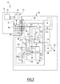
- an electronic trip unit 10 of a circuit breaker is connected to a removable device 20 via a communication bus 30.
- the removable device 20 is also connected, by a wireless link 35, to a supervision apparatus 40.
- the electronic release 10 comprises a protective housing 52 having a plurality of walls 53.
- the trigger 10 comprises a power supply 54, an internal power supply bus 55 and a first processing unit 56, such as a microprocessor, arranged at the
- the trigger 10 comprises an electrical connector 58, for connecting the removable device 20, the connector 58 being received in an orifice 59 formed in one of the walls 53, preferably in a wall 53 accessible from outside when the trigger 10 is installed in an electrical panel.
- the removable device 20 is, for example, a communication module, and comprises, a connector 60 complementary to the connector 58, a second processing unit 62, a radio communication module 64 comprising a radio transceiver 66, and a device 68 of taking electrical energy from the internal supply bus 55.
- the removable device 20 is able to be connected / disconnected at plug and play of the electronic release 10, without the risk of trigger 10 malfunction.
- the supervision apparatus 40 also called a concentrator, is able to communicate with the removable device 20 in order to centralize information received from the different triggers 10 and to supervise each of the triggers 10.
- the supervision apparatus 40 comprises a radio transceiver 72 and is intended to be powered by an external power supply 74.
- the supervision apparatus 40 is clean, via its radio transceiver 72, in transmitting an information sending command or time synchronization message, to the removable device 20, and more specifically to the radiocommunication module 64 which is capable of transmitting this message to the second processing unit 62.
- the power supply 54 is represented more precisely at figure 3 , in the case where the circuit breaker 10 is connected to a three-phase network comprising three phase wires 82, 84 and 86.
- the electrical power supply 54 comprises, for each of the phase wires 82, 84, 86, a torus 90 arranged around the phase wires 82, 84, 86 corresponding and a winding 92 arranged around each torus 90.
- the flow of the current in the corresponding phase wires 82, 84 and 86 is able to generate an induced current in each winding 92.
- the trigger 10 is self-powered by the cores 90 and the windings 92, which recover the magnetic energy of the three-phase network and form current transformers.
- Each torus 90 is an iron torus.
- the power supply 54 also comprises a converter 93, such as a Graetz bridge-type rectifier, connected to each of the windings 92, and to an electric ground M, the converter 93 being able to deliver a positive voltage.
- a converter 93 such as a Graetz bridge-type rectifier
- the power supply 54 comprises a diode D1b, a chopper 94, a capacitor C1 for supplying the trigger and a control member 95 for chopper 94.
- A1 denotes an output of the converter 93 which is connected to the chopper 94 which is itself connected to the ground M.
- the chopper 94 is also connected to a terminal of the supply capacitor C1 via the diode D1b, l other terminal of the capacitor C1 being connected to the ground M.
- A2 an output of the diode D1b connected to the terminal of the capacitor C1.
- the control block 95 of the chopper 94 is connected in parallel with the supply capacitor C1, the chopper 94 and the control block 95 being connected via an electrical connection 96. At the output A1, a first signal is provided. S1 supply and output A2 a second signal S2.
- the internal power supply bus 55 is arranged between the power supply 54 and the connector 58, and is capable of transmitting the supply signal S1 to the connector 58.
- the first processing unit 56 is able to recover the information relating to the currents flowing in each phase wire 82, 84, 86, the currents being measured by means of current sensors positioned around each phase wire 82, 84, 86.
- the cores 90 associated with the windings 92 are clean in some cases to play the role of current sensors.
- the first processing unit 56 is able to also calculate the powers and electrical energy from the received and measured current values. I note the information relating to the values of current, energy and power measured or calculated by the first processing unit 56.
- the connector 58 is accessible from outside the housing 53, preferably from a front face of the electrical panel when the trigger 10 is installed in said table. As visible at figure 2
- the connector 58 comprises three output terminals, noted respectively 99, 100 and 101.
- the first output terminal 99 corresponds to the first supply signal S1.
- the second output terminal 100 corresponds to the mass M, and the third output terminal 101 corresponds to the information I.
- the first output terminal 99 and the second output terminal 100 are directly connected to the electrical energy sampling device. 68, via the communication bus 30 and the connector 60.
- the third output terminal 101 is directly connected to the second processing unit 62, via the communication bus 30 and the connector 60.
- the connector 60 is a connector complementary to the connector 58.
- the connector 58 is, for example, a socket, and the connector 60 is then a plug.
- the second processing unit 62 is able to recover the information I, via the connection between the connectors 58 and 60, and is able to transmit this information to the radiocommunication module 64.
- the radiocommunication module 64 is clean, via its radio transceiver 66, to transmit the information I to the supervision apparatus 40 via the wireless link 35 arranged between the transceiver 66 and the transmitter -receiver 72.
- the radio transceiver 66 is preferably in accordance with the ZIGBEE or ZIGBEE green power communication protocol, based on the IEEE-802.15 standard. In a variant, the radio transceiver 66 complies with the IEEE-802.15.1 standard. or IEEE-802.15.2. In another variant, the transceiver radio 66 is preferably in accordance with the IEEE-802-11 standard. In another variant, without meeting an IEEE standard, this transceiver 66 complies with the regulations in force in each country.
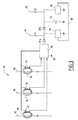
- the electrical energy harvesting device 68 is shown in FIG. figure 2 in more detail than in the figure 1 and according to one embodiment of the invention.
- the electrical energy sampling device 68 comprises detection means 102 and a generator 104 of a first reference voltage V 1ref .
- the sampling member 68 further comprises means 106 for comparing voltages.
- the sampling member 68 also comprises means 108 for taking electrical energy from the supply bus 55.
- the radio transceiver 72 is similar to the radio transceiver 66, so that the wireless radio communication 35 is established between the removable device 20 and the supervision apparatus 40, and more particularly between the radio module 64 and the supervision apparatus 40.
- the detection means 102 comprise a diode D2 connected in parallel with a resistor R2, and a capacitor C2 connected in series with the resistor R2.
- the detection means 102 correspond to a differentiator circuit formed by the capacitor C2 and the resistor R2, and are directly connected to the first output terminal 99 corresponding to the first signal S1.
- the detection means 102 are able to detect each rising edge of the supply signal S1, the signal S1 being delivered by the power supply bus 55 via the connection between the connectors 58 and 60.
- the common terminal between the diode D2, the capacitor C2 and the resistor R2 is capable of delivering a third signal S3.
- the generator 104 of the first reference voltage V 1ref comprises a capacitor C3, a resistor R3, a diode D3 and a component 112 which generates the first reference voltage V 1ref .
- the comparison means 106 are, for example, formed by an operational amplifier AOP whose first non-inverting input 114 is connected to the common terminal between the diode D2, the capacitor C2 and the resistor R2.
- the amplifier AOP also comprises an inverting input 116 on which the first reference voltage V 1ref is delivered, the inverting input 116 being connected to the generator 104.
- the operational amplifier AOP is supplied from the capacitor C3.
- the comparison means 106 are suitable for comparing the third signal S3 with the first reference voltage V 1ref .
- the sampling means 108 are directly connected to the first output 99 and comprise a resistor R4 and a diode D4 connected in series to the source a transistor T, and a capacitor C4 connected to the drain of the transistor T.
- the gate of the transistor T is connected to the output 117 of the amplifier AOP.
- the sampling means 108 are able to take the electrical energy delivered by the internal power supply bus 55.
- Bindings 114 and 116 of the sampling means 108 with respectively the second processing unit 62 and the radiocommunication block 64 form means for transmitting the electrical energy taken by the sampling means 108.
- the second signal S2, at the output A2 of the power supply 54, is suitable for supplying the trigger 10, while the first signal S1, at the output A1, is suitable for being delivered to the removable device 20 and to the sampling member. 68 through the power bus 55, the communication bus 30 and the connectors 58 and 60.
- the first signal S1 allows the supply of the removable device 20.
- the power supply 54 is a switching power supply. More specifically, when closing the contacts of the circuit breaker comprising the trigger 10, the voltage of each signal S1, S2 increases because the supply capacitor C1 of the trigger 10 is being loaded. Then as soon as the voltage across the capacitor C1 is greater than a second reference voltage V 2ref predetermined, the hash of the power supply 54 and the first supply signal S1, by the chopper 94, is triggered by the control block 95. Thus, as soon as the first signal S1 and the second signal S2 have reached the second reference voltage V 2ref of predetermined value, the control block 95 triggers the chopper 94. In effect, the block 95 controls the chopper 94, which is equivalent, for example, to a CMOS transistor, in an on or off state.
- the control block 95 controls the chopper 94 according to the value of the voltage of the second signal S2 output A2, that is to say across the capacitor C1.
- the chopper 94 is controlled in order to short-circuit the power supply 54, that is to say to set the voltage of the first signal S1 to a value zero, which corresponds to a low state.
- the chopper 94 is controlled so as not to short-circuit the power supply 54. That is to say, so that the power supply 54 charges the capacitor C1 and that the first signal S1 has a voltage value substantially equivalent to the voltage of the second signal S2. This corresponds to a high state of the first signal S1.
- the supply capacitor C1 of the trip unit 10 is charged when the voltage of the second signal S2 is greater than the second reference voltage V 2ref , and then discharges when the signal S1 is at the low state and that the trigger 10, more specifically the first processing unit 56, consumes current.
- the second signal S2 successively corresponds to a charge, then to a discharge of the capacitor C1, while the first signal S1 is successively in the high state and then in the low state.
- the signal S1 therefore comprises successive pulses in voltage.
- the electrical energy stored by the capacitor C1 is sufficient, it is therefore no longer necessary to charge the capacitor C1 and the power supply 54 may be short. circuited. Then, after a certain period of time which is generally constant, since the consumption of the trigger 10 is globally constant, the short circuit is reopened in order to recharge the capacitor C1 for supplying the trigger 10.
- the detection means 102 are then able to detect rising edges of the supply signal S1 delivered by the power supply bus 55.
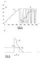
- the capacitor C2 will load and transmit on the input 114 of the AOP amplifier the third signal S3 corresponding globally to the derivative of the signal S1.
- the third signal S3 therefore has a high voltage value at this time.
- the voltage of the third signal S3 decreases exponentially, with a time constant equal to the product of the value of the resistance R2 and capacitance of the capacitor C2.
- the capacitor C2 discharges through the diode D2.
- the operational amplifier AOP has on the non-inverting input 114 the third signal S3 and on the inverting input 116 the first reference voltage V 1ref .
- the voltage of the third signal S3 is greater than the first reference voltage V 1ref as shown in FIG. figure 5 , and the output 117 of the operational amplifier AOP is in the high state.
- the supply signal S1 stabilizes, that is to say that the load of the supply capacitor C1 of the trip unit 10 is terminated
- the voltage of the third signal S3 is lower than the first reference voltage V 1ref and the output 117 of the amplifier AOP goes low.
- the evolution of the state of the output 117 as a function of the state of the first signal S1 and of the time is represented in FIG. figure 5 by an OUT curve.
- the evolution of the output 117 of the amplifier AOP makes it possible to turn the transistor T successively, then blocking. Indeed, the output of the amplifier AOP is successively in the high state, and in this case the transistor T is passing, then in the low state, and in this case the transistor T is blocking.
- the transistor T is on, the capacitor C4 draws energy from the supply signal S1 and charges, whereas when the transistor T is blocking, the capacitor C4 gradually discharges.
- the transistor T used in this embodiment is, for example, a MOS transistor.
- the sampling member 68 is able to take the electrical energy of the supply signal S1, since the detection of a rising edge and as long as the third signal S3 has a voltage greater than the first reference voltage V 1ref .
- the third signal S3 is equivalent to a signal for triggering the collection of the electrical energy of the signal S1 by the sampling means 108. Indeed, the third signal S3 makes it possible to control the output 117 of the amplifier AOP and therefore the state of the transistor T.
- a fourth signal S4 representing the voltage across the capacitor C4 as a function of time is shown.
- the capacitor C4 charges, when the supply signal S1 is high and the output 117 of the AOP is high. In other words, it takes electrical energy on the internal power supply bus 55 and the first signal S1.
- the capacitor C4 discharges when the supply signal S1 is low or the output 117 of the AOP is low. In other words, it does not take electrical energy from the internal power supply bus 55 and it gradually discharges in order to supply, thanks to the signal S4, the second processing unit 62 and the radiocommunication module 64.
- periods P during which the capacitor C4 charges that is to say during which the sampling means 108 draw energy on the signal S1 are not necessarily of constant duration.
- the time during which electrical energy is taken from the signal S1 power supply is always less than the time during which the signal S1 is high.
- the third signal S3 has its voltage which increases strongly and then decreases exponentially.
- the output 117 which corresponds to the OUT curve is then in the high state and the transistor T is on which allows the charging of the capacitor C4.
- the moment when the first signal S1 goes to the high state corresponds to the beginning of the period P.
- the output 117 goes to the low state , the transistor T becomes blocking and the capacitor C4 then discharges. This instant corresponds to the end of the period P.
- the duration of each period P, and therefore of the capacitor C4 taking the electrical energy delivered by the first signal S1 depends on the moment when the third signal S3 has a voltage lower than the first reference voltage V 1ref .
- the widths of the pulses of the signal S1 are variable since the supply current of the capacitor C1 is sinusoidal. Thus, at each rising edge of the signal S1, the value of the current for charging the capacitor C1 is not always the same. This implies that the charge of the capacitor C1 is longer or shorter and that the supply signal S1 is high for more or less long time.
- sampling device 68 corresponds to an analog solution.
- collection of energy is performed digitally using a microcontroller.
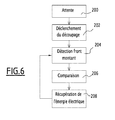
- a method of supplying the removable device 20 from the power supply 54, visible to the figure 6 comprises a first step 200 during which, when closing the circuit breaker, it is expected that the first signal S1 reaches at least once the second reference voltage V 2ref .
- a second step 202 consists in triggering the hash of the power supply 54 and thus of the signal S1 once the first signal S1 has reached the second reference voltage V 2ref .
- a third step 204 consists in detecting a rising edge of the supply signal S1 by the detection means 102.
- This third step 204 is followed by a fourth step 206 for comparing the third signal S3, also called the trigger signal, with the first reference voltage V 1ref .
- This fourth step 206 is performed using the comparison means 106.
- the sampling means 108 take electrical energy from the supply bus 55 and the supply signal S1 as long as the third signal S3 has a value greater than that of the first reference voltage V 1ref . Following the sampling step 208, it returns to the detection step 204 as the circuit breaker 10 remains closed.
- the first step 200 generally takes place at the closing of the circuit breaker 10 once the supply capacitor C1 is charged and the supply signal S1 has reached the second reference voltage V 2ref .
- the invention thus makes it possible to take electrical energy from the internal supply bus 55 of the electronic trip unit 10 without disturbing the measurement of the current or the operation of the trip unit 10, and more particularly of its processing unit 56.
- the trigger 10 is supplied with priority and the removable device 20 does not work.
- the sampling means 108 take electrical energy from the signal S2 only when the capacitor C1 of the trigger 10 is loaded and the first processing unit 56 operates. It is indeed at this time that the chopping, or cutting, of the power supply 54 is triggered, since the capacitor C1 of the trigger 10 has stored enough energy to supply the trigger 10, and that it is therefore no longer necessary to charge the capacitor C1 continuously.
- the removable module 20 takes electrical energy from the supply signal S1 globally at each pulse of the signal S1. This makes it possible to charge its capacitor C4 which supplies the second processing unit 62 and the radiocommunication module 64. After several hashing sequences, that is to say after several pulses of the signal S1, the capacitor C4 is charged and the signal voltage S4 is equal to or slightly less than the signal voltage S1, when in the high state.
- the removable device 20 takes energy from the power supply 54 only at the appearance of a rising edge, that is to say, during a pulse that appears once the chopper 94 is operating and chopping signal S1, and during the charging of the capacitor C1. The operation of the trigger 10 is thus not disturbed by the electrical energy taken by the sampling member 68.
- voltage dividers are added in the pick-up device 68 to limit the voltage values of the signal S4 to values compatible with the power supply of the second processing unit 62 and the radio communication module 64.
- the signal S4 transmitted by the capacitor C4 to the second processing unit 62 and to the radiocommunication module 64 is, in addition, chopped to have an average DC voltage of suitable value.
- the invention presented above allows a progressive charging of the capacitor C4 and the communication is established from time to time, that is to say for example every second, between the radiocommunication module 64 and the supervision apparatus 40 in order to exchange current, power, energy or other information concerning an electrical installation equipped with the circuit breaker 10.
- the radiocommunication module 64 and the processing unit 62 consume the electrical energy stored in the capacitor C4, every second. Between these consumption periods, the capacitor C4 is charged from the supply signal S1, as shown above, and the processing unit 62 and the radiocommunication module 64 consume little.
- the trigger 10 further allows the measurement of currents and the opening of the contacts of the circuit breaker, if an overcurrent is detected.
- the capacitor C4 has a high capacity, of the order for example of six microfarads ( ⁇ F) to store a large amount of electrical energy.
- the number of pulses, that is to say, hash sequences, necessary for the charging of the capacitor C4 is a function of the first signal S1, the values of the resistance R2, the capacitance of the capacitor C2 and the capacitor C2. the first reference voltage V 1ref .
- the electronic release 10 is not powered from tori 90 and windings 92, but by an auxiliary power supply.
- the removable device does not allow radio communication as shown below, but a wired communication or simply an information display on a screen.
- the time during which the capacitor C4 is charged is constant and set at a value equal to the shortest possible time for a pulse of the signal S1.
Landscapes
- Breakers (AREA)
- Emergency Protection Circuit Devices (AREA)
Applications Claiming Priority (1)
| Application Number | Priority Date | Filing Date | Title |
|---|---|---|---|
| FR1356134A FR3007902B1 (fr) | 2013-06-26 | 2013-06-26 | Dispositif amovible pour declencheur electronique, procede d'alimentation d'un tel dispositif et ensemble comportant un declencheur electronique et un tel dispositif amovible |
Publications (2)
| Publication Number | Publication Date |
|---|---|
| EP2822018A1 true EP2822018A1 (de) | 2015-01-07 |
| EP2822018B1 EP2822018B1 (de) | 2018-04-04 |
Family
ID=49753264
Family Applications (1)
| Application Number | Title | Priority Date | Filing Date |
|---|---|---|---|
| EP14173797.3A Active EP2822018B1 (de) | 2013-06-26 | 2014-06-25 | Entfernbare Vorrichtung für elektronischen Auslöser, Verfahren zur Stromversorgung einer solchen Vorrichtung, und Einheit, die einen solchen elektronischen Auslöser und eine solche entfernbare Vorrichtung umfasst |
Country Status (4)
| Country | Link |
|---|---|
| US (1) | US9576763B2 (de) |
| EP (1) | EP2822018B1 (de) |
| CN (1) | CN104253000B (de) |
| FR (1) | FR3007902B1 (de) |
Cited By (1)
| Publication number | Priority date | Publication date | Assignee | Title |
|---|---|---|---|---|
| FR3055420A1 (fr) * | 2016-08-31 | 2018-03-02 | Schneider Electric Ind Sas | Unite de controle d'un disjoncteur electrique et disjoncteur comportant une telle unite de controle |
Citations (5)
| Publication number | Priority date | Publication date | Assignee | Title |
|---|---|---|---|---|
| EP0843332A1 (de) * | 1996-11-15 | 1998-05-20 | Schneider Electric Sa | Lastschalter mit einem Leistungsschalterblock mit Bearbeitungs-Modul, Kalibrierungs-Modul und Anzeige-Modul |
| WO1999036928A1 (en) * | 1998-01-14 | 1999-07-22 | General Electric Company | Circuit breaker having hall effect sensors |
| EP1347485A1 (de) * | 2002-03-19 | 2003-09-24 | Schneider Electric Industries SAS | Zusatzeinheit für eine Schaltschütz |
| EP1596206A1 (de) * | 2004-05-13 | 2005-11-16 | Schneider Electric Industries Sas | Elektrische Strommessanordnung, Stromsensor, elektrischer Auslöser und Trennschalter mit einer derartigen Strommessanordnung |
| WO2012007831A2 (en) * | 2010-07-16 | 2012-01-19 | Levelation | Circuit breaker with integral meter and wireless communications |
Family Cites Families (1)
| Publication number | Priority date | Publication date | Assignee | Title |
|---|---|---|---|---|
| US8488302B2 (en) * | 2011-04-14 | 2013-07-16 | Eaton Corporation | Circuit breaker panel |
-
2013
- 2013-06-26 FR FR1356134A patent/FR3007902B1/fr not_active Expired - Fee Related
-
2014
- 2014-06-13 US US14/304,118 patent/US9576763B2/en active Active
- 2014-06-25 EP EP14173797.3A patent/EP2822018B1/de active Active
- 2014-06-26 CN CN201410299127.8A patent/CN104253000B/zh active Active
Patent Citations (6)
| Publication number | Priority date | Publication date | Assignee | Title |
|---|---|---|---|---|
| EP0843332A1 (de) * | 1996-11-15 | 1998-05-20 | Schneider Electric Sa | Lastschalter mit einem Leistungsschalterblock mit Bearbeitungs-Modul, Kalibrierungs-Modul und Anzeige-Modul |
| FR2756095A1 (fr) | 1996-11-15 | 1998-05-22 | Schneider Electric Sa | Disjoncteur avec un bloc disjoncteur et des modules de traitement, de calibrage et de communication |
| WO1999036928A1 (en) * | 1998-01-14 | 1999-07-22 | General Electric Company | Circuit breaker having hall effect sensors |
| EP1347485A1 (de) * | 2002-03-19 | 2003-09-24 | Schneider Electric Industries SAS | Zusatzeinheit für eine Schaltschütz |
| EP1596206A1 (de) * | 2004-05-13 | 2005-11-16 | Schneider Electric Industries Sas | Elektrische Strommessanordnung, Stromsensor, elektrischer Auslöser und Trennschalter mit einer derartigen Strommessanordnung |
| WO2012007831A2 (en) * | 2010-07-16 | 2012-01-19 | Levelation | Circuit breaker with integral meter and wireless communications |
Cited By (3)
| Publication number | Priority date | Publication date | Assignee | Title |
|---|---|---|---|---|
| FR3055420A1 (fr) * | 2016-08-31 | 2018-03-02 | Schneider Electric Ind Sas | Unite de controle d'un disjoncteur electrique et disjoncteur comportant une telle unite de controle |
| EP3290935A1 (de) * | 2016-08-31 | 2018-03-07 | Schneider Electric Industries SAS | Kontrolleinheit eines elektrischen trennschalters, und trennschalter, der eine solche kontrolleinheit umfasst |
| US10908215B2 (en) | 2016-08-31 | 2021-02-02 | Schneider Electric Industries Sas | Monitoring unit for monitoring an electrical circuit breaker and circuit breaker comprising such a monitoring unit |
Also Published As
| Publication number | Publication date |
|---|---|
| CN104253000A (zh) | 2014-12-31 |
| CN104253000B (zh) | 2018-01-30 |
| FR3007902A1 (fr) | 2015-01-02 |
| FR3007902B1 (fr) | 2015-07-24 |
| US9576763B2 (en) | 2017-02-21 |
| US20150002246A1 (en) | 2015-01-01 |
| EP2822018B1 (de) | 2018-04-04 |
Similar Documents
| Publication | Publication Date | Title |
|---|---|---|
| EP4189766B1 (de) | Modulares, in serie geschaltetes batteriepack (blmose) | |
| EP2849196B1 (de) | Verfahren zur Erkennung der Ursache eines Spannungsverlusts vor einem Trennschalter, Hilfsgerät für Trennschalter sowie elektrisches System, das einen solchen Trennschalter und ein solches Hilfsgerät umfasst | |
| EP1685636B2 (de) | Tragbares selbständiges elektrowerkzeug | |
| CA2594826C (fr) | Procede de chargement equilibre d'une batterie lithium-ion ou lithium polymere | |
| EP2721684B1 (de) | Batteriezellensystem mit vereinfachter überwachung | |
| FR2973963A1 (fr) | Dispositif de transfert de charge et procede de gestion associe | |
| EP4189406B1 (de) | Batterieverwaltungssystem | |
| EP3707521B1 (de) | Verfahren zur erkennung des zustandes eines elektronischen schutzgeräts in einer elektrischen anlage und detektor mit diesem verfahren | |
| EP4134695A1 (de) | Überprüfung der messgenauigkeit eines stromzählers | |
| EP2822018B1 (de) | Entfernbare Vorrichtung für elektronischen Auslöser, Verfahren zur Stromversorgung einer solchen Vorrichtung, und Einheit, die einen solchen elektronischen Auslöser und eine solche entfernbare Vorrichtung umfasst | |
| EP3719947B1 (de) | Elektrische schutzverfahren und - systeme | |
| EP3639344A1 (de) | Verfahren zum laden von batterien für ein flugzeug und system zum speichern von strom | |
| EP3420784B1 (de) | System zur steuerung der stromversorgung einer spannungsquelle für elektrozaun und verfahren zum betrieb solch eines systems | |
| WO2016142628A1 (fr) | Carte électronique de pilotage énergétique d'un équipement électrique autonome et communicant | |
| EP4350925B1 (de) | Überwachung und optimierung des stromverbrauchs | |
| EP2626881B1 (de) | Elektrisches Sicherheitsverfahren und -vorrichtung für Erdschluss | |
| FR3018006A1 (fr) | Systeme de commutation controlee pour le raccordement selectif d'un reseau electrique triphase | |
| EP3583618B1 (de) | Schutzschalter | |
| FR3021816A1 (fr) | Chargeur de batterie pour vehicule automobile electrique a moyens de compensation passive variables et procede de commande d'un tel chargeur | |
| EP2693585B1 (de) | Schutzsystem für eine Vielzahl von elektrischen Ableitungen gegen Kurzschlüsse, und Elektroanlage, die ein solches Schutzsystem umfasst | |
| EP4492598A1 (de) | Verfahren zur überprüfung der eignung für restströme von differentialschutzschaltern | |
| FR2975237A1 (fr) | Circuit de protection contre une surintensite | |
| EP2533391A2 (de) | Multi-Source-Steuerungssystem von Stromgeneratoren | |
| EP3511970A1 (de) | Elektrischer schalter mit einem detektor welcher informationen über die auslösung des schalters in einen bus einspeist | |
| FR2802031A1 (fr) | Dispositif bloc autonome d'eclairage de securite et d'alarme et installation utilisant un tel dispositif |
Legal Events
| Date | Code | Title | Description |
|---|---|---|---|
| PUAI | Public reference made under article 153(3) epc to a published international application that has entered the european phase |
Free format text: ORIGINAL CODE: 0009012 |
|
| 17P | Request for examination filed |
Effective date: 20140625 |
|
| AK | Designated contracting states |
Kind code of ref document: A1 Designated state(s): AL AT BE BG CH CY CZ DE DK EE ES FI FR GB GR HR HU IE IS IT LI LT LU LV MC MK MT NL NO PL PT RO RS SE SI SK SM TR |
|
| AX | Request for extension of the european patent |
Extension state: BA ME |
|
| R17P | Request for examination filed (corrected) |
Effective date: 20150609 |
|
| RBV | Designated contracting states (corrected) |
Designated state(s): AL AT BE BG CH CY CZ DE DK EE ES FI FR GB GR HR HU IE IS IT LI LT LU LV MC MK MT NL NO PL PT RO RS SE SI SK SM TR |
|
| REG | Reference to a national code |
Ref country code: DE Ref legal event code: R079 Ref document number: 602014023213 Country of ref document: DE Free format text: PREVIOUS MAIN CLASS: H01H0071020000 Ipc: H01H0071120000 |
|
| GRAP | Despatch of communication of intention to grant a patent |
Free format text: ORIGINAL CODE: EPIDOSNIGR1 |
|
| RIC1 | Information provided on ipc code assigned before grant |
Ipc: H01H 71/12 20060101AFI20171130BHEP Ipc: H02J 13/00 20060101ALN20171130BHEP Ipc: H01H 71/02 20060101ALI20171130BHEP |
|
| INTG | Intention to grant announced |
Effective date: 20180104 |
|
| GRAS | Grant fee paid |
Free format text: ORIGINAL CODE: EPIDOSNIGR3 |
|
| GRAA | (expected) grant |
Free format text: ORIGINAL CODE: 0009210 |
|
| AK | Designated contracting states |
Kind code of ref document: B1 Designated state(s): AL AT BE BG CH CY CZ DE DK EE ES FI FR GB GR HR HU IE IS IT LI LT LU LV MC MK MT NL NO PL PT RO RS SE SI SK SM TR |
|
| REG | Reference to a national code |
Ref country code: GB Ref legal event code: FG4D Free format text: NOT ENGLISH |
|
| REG | Reference to a national code |
Ref country code: CH Ref legal event code: EP |
|
| REG | Reference to a national code |
Ref country code: AT Ref legal event code: REF Ref document number: 986449 Country of ref document: AT Kind code of ref document: T Effective date: 20180415 |
|
| REG | Reference to a national code |
Ref country code: IE Ref legal event code: FG4D Free format text: LANGUAGE OF EP DOCUMENT: FRENCH |
|
| REG | Reference to a national code |
Ref country code: DE Ref legal event code: R096 Ref document number: 602014023213 Country of ref document: DE |
|
| REG | Reference to a national code |
Ref country code: FR Ref legal event code: PLFP Year of fee payment: 5 |
|
| REG | Reference to a national code |
Ref country code: NL Ref legal event code: MP Effective date: 20180404 |
|
| REG | Reference to a national code |
Ref country code: LT Ref legal event code: MG4D |
|
| PG25 | Lapsed in a contracting state [announced via postgrant information from national office to epo] |
Ref country code: NL Free format text: LAPSE BECAUSE OF FAILURE TO SUBMIT A TRANSLATION OF THE DESCRIPTION OR TO PAY THE FEE WITHIN THE PRESCRIBED TIME-LIMIT Effective date: 20180404 |
|
| PG25 | Lapsed in a contracting state [announced via postgrant information from national office to epo] |
Ref country code: PL Free format text: LAPSE BECAUSE OF FAILURE TO SUBMIT A TRANSLATION OF THE DESCRIPTION OR TO PAY THE FEE WITHIN THE PRESCRIBED TIME-LIMIT Effective date: 20180404 Ref country code: SE Free format text: LAPSE BECAUSE OF FAILURE TO SUBMIT A TRANSLATION OF THE DESCRIPTION OR TO PAY THE FEE WITHIN THE PRESCRIBED TIME-LIMIT Effective date: 20180404 Ref country code: FI Free format text: LAPSE BECAUSE OF FAILURE TO SUBMIT A TRANSLATION OF THE DESCRIPTION OR TO PAY THE FEE WITHIN THE PRESCRIBED TIME-LIMIT Effective date: 20180404 Ref country code: NO Free format text: LAPSE BECAUSE OF FAILURE TO SUBMIT A TRANSLATION OF THE DESCRIPTION OR TO PAY THE FEE WITHIN THE PRESCRIBED TIME-LIMIT Effective date: 20180704 Ref country code: AL Free format text: LAPSE BECAUSE OF FAILURE TO SUBMIT A TRANSLATION OF THE DESCRIPTION OR TO PAY THE FEE WITHIN THE PRESCRIBED TIME-LIMIT Effective date: 20180404 Ref country code: BG Free format text: LAPSE BECAUSE OF FAILURE TO SUBMIT A TRANSLATION OF THE DESCRIPTION OR TO PAY THE FEE WITHIN THE PRESCRIBED TIME-LIMIT Effective date: 20180704 Ref country code: ES Free format text: LAPSE BECAUSE OF FAILURE TO SUBMIT A TRANSLATION OF THE DESCRIPTION OR TO PAY THE FEE WITHIN THE PRESCRIBED TIME-LIMIT Effective date: 20180404 Ref country code: LT Free format text: LAPSE BECAUSE OF FAILURE TO SUBMIT A TRANSLATION OF THE DESCRIPTION OR TO PAY THE FEE WITHIN THE PRESCRIBED TIME-LIMIT Effective date: 20180404 |
|
| PG25 | Lapsed in a contracting state [announced via postgrant information from national office to epo] |
Ref country code: HR Free format text: LAPSE BECAUSE OF FAILURE TO SUBMIT A TRANSLATION OF THE DESCRIPTION OR TO PAY THE FEE WITHIN THE PRESCRIBED TIME-LIMIT Effective date: 20180404 Ref country code: GR Free format text: LAPSE BECAUSE OF FAILURE TO SUBMIT A TRANSLATION OF THE DESCRIPTION OR TO PAY THE FEE WITHIN THE PRESCRIBED TIME-LIMIT Effective date: 20180705 Ref country code: LV Free format text: LAPSE BECAUSE OF FAILURE TO SUBMIT A TRANSLATION OF THE DESCRIPTION OR TO PAY THE FEE WITHIN THE PRESCRIBED TIME-LIMIT Effective date: 20180404 Ref country code: RS Free format text: LAPSE BECAUSE OF FAILURE TO SUBMIT A TRANSLATION OF THE DESCRIPTION OR TO PAY THE FEE WITHIN THE PRESCRIBED TIME-LIMIT Effective date: 20180404 |
|
| REG | Reference to a national code |
Ref country code: AT Ref legal event code: MK05 Ref document number: 986449 Country of ref document: AT Kind code of ref document: T Effective date: 20180404 |
|
| PG25 | Lapsed in a contracting state [announced via postgrant information from national office to epo] |
Ref country code: PT Free format text: LAPSE BECAUSE OF FAILURE TO SUBMIT A TRANSLATION OF THE DESCRIPTION OR TO PAY THE FEE WITHIN THE PRESCRIBED TIME-LIMIT Effective date: 20180806 |
|
| REG | Reference to a national code |
Ref country code: DE Ref legal event code: R097 Ref document number: 602014023213 Country of ref document: DE |
|
| PG25 | Lapsed in a contracting state [announced via postgrant information from national office to epo] |
Ref country code: DK Free format text: LAPSE BECAUSE OF FAILURE TO SUBMIT A TRANSLATION OF THE DESCRIPTION OR TO PAY THE FEE WITHIN THE PRESCRIBED TIME-LIMIT Effective date: 20180404 Ref country code: CZ Free format text: LAPSE BECAUSE OF FAILURE TO SUBMIT A TRANSLATION OF THE DESCRIPTION OR TO PAY THE FEE WITHIN THE PRESCRIBED TIME-LIMIT Effective date: 20180404 Ref country code: EE Free format text: LAPSE BECAUSE OF FAILURE TO SUBMIT A TRANSLATION OF THE DESCRIPTION OR TO PAY THE FEE WITHIN THE PRESCRIBED TIME-LIMIT Effective date: 20180404 Ref country code: AT Free format text: LAPSE BECAUSE OF FAILURE TO SUBMIT A TRANSLATION OF THE DESCRIPTION OR TO PAY THE FEE WITHIN THE PRESCRIBED TIME-LIMIT Effective date: 20180404 Ref country code: RO Free format text: LAPSE BECAUSE OF FAILURE TO SUBMIT A TRANSLATION OF THE DESCRIPTION OR TO PAY THE FEE WITHIN THE PRESCRIBED TIME-LIMIT Effective date: 20180404 Ref country code: SK Free format text: LAPSE BECAUSE OF FAILURE TO SUBMIT A TRANSLATION OF THE DESCRIPTION OR TO PAY THE FEE WITHIN THE PRESCRIBED TIME-LIMIT Effective date: 20180404 |
|
| REG | Reference to a national code |
Ref country code: CH Ref legal event code: PL |
|
| PLBE | No opposition filed within time limit |
Free format text: ORIGINAL CODE: 0009261 |
|
| STAA | Information on the status of an ep patent application or granted ep patent |
Free format text: STATUS: NO OPPOSITION FILED WITHIN TIME LIMIT |
|
| PG25 | Lapsed in a contracting state [announced via postgrant information from national office to epo] |
Ref country code: SM Free format text: LAPSE BECAUSE OF FAILURE TO SUBMIT A TRANSLATION OF THE DESCRIPTION OR TO PAY THE FEE WITHIN THE PRESCRIBED TIME-LIMIT Effective date: 20180404 |
|
| REG | Reference to a national code |
Ref country code: BE Ref legal event code: MM Effective date: 20180630 |
|
| 26N | No opposition filed |
Effective date: 20190107 |
|
| REG | Reference to a national code |
Ref country code: IE Ref legal event code: MM4A |
|
| GBPC | Gb: european patent ceased through non-payment of renewal fee |
Effective date: 20180704 |
|
| PG25 | Lapsed in a contracting state [announced via postgrant information from national office to epo] |
Ref country code: MC Free format text: LAPSE BECAUSE OF FAILURE TO SUBMIT A TRANSLATION OF THE DESCRIPTION OR TO PAY THE FEE WITHIN THE PRESCRIBED TIME-LIMIT Effective date: 20180404 Ref country code: LU Free format text: LAPSE BECAUSE OF NON-PAYMENT OF DUE FEES Effective date: 20180625 |
|
| PG25 | Lapsed in a contracting state [announced via postgrant information from national office to epo] |
Ref country code: LI Free format text: LAPSE BECAUSE OF NON-PAYMENT OF DUE FEES Effective date: 20180630 Ref country code: GB Free format text: LAPSE BECAUSE OF NON-PAYMENT OF DUE FEES Effective date: 20180704 Ref country code: CH Free format text: LAPSE BECAUSE OF NON-PAYMENT OF DUE FEES Effective date: 20180630 Ref country code: IE Free format text: LAPSE BECAUSE OF NON-PAYMENT OF DUE FEES Effective date: 20180625 |
|
| PG25 | Lapsed in a contracting state [announced via postgrant information from national office to epo] |
Ref country code: SI Free format text: LAPSE BECAUSE OF FAILURE TO SUBMIT A TRANSLATION OF THE DESCRIPTION OR TO PAY THE FEE WITHIN THE PRESCRIBED TIME-LIMIT Effective date: 20180404 Ref country code: BE Free format text: LAPSE BECAUSE OF NON-PAYMENT OF DUE FEES Effective date: 20180630 |
|
| PG25 | Lapsed in a contracting state [announced via postgrant information from national office to epo] |
Ref country code: MT Free format text: LAPSE BECAUSE OF FAILURE TO SUBMIT A TRANSLATION OF THE DESCRIPTION OR TO PAY THE FEE WITHIN THE PRESCRIBED TIME-LIMIT Effective date: 20180404 |
|
| PG25 | Lapsed in a contracting state [announced via postgrant information from national office to epo] |
Ref country code: TR Free format text: LAPSE BECAUSE OF FAILURE TO SUBMIT A TRANSLATION OF THE DESCRIPTION OR TO PAY THE FEE WITHIN THE PRESCRIBED TIME-LIMIT Effective date: 20180404 |
|
| PG25 | Lapsed in a contracting state [announced via postgrant information from national office to epo] |
Ref country code: HU Free format text: LAPSE BECAUSE OF FAILURE TO SUBMIT A TRANSLATION OF THE DESCRIPTION OR TO PAY THE FEE WITHIN THE PRESCRIBED TIME-LIMIT; INVALID AB INITIO Effective date: 20140625 |
|
| PG25 | Lapsed in a contracting state [announced via postgrant information from national office to epo] |
Ref country code: CY Free format text: LAPSE BECAUSE OF FAILURE TO SUBMIT A TRANSLATION OF THE DESCRIPTION OR TO PAY THE FEE WITHIN THE PRESCRIBED TIME-LIMIT Effective date: 20180404 Ref country code: MK Free format text: LAPSE BECAUSE OF NON-PAYMENT OF DUE FEES Effective date: 20180404 |
|
| PG25 | Lapsed in a contracting state [announced via postgrant information from national office to epo] |
Ref country code: IS Free format text: LAPSE BECAUSE OF FAILURE TO SUBMIT A TRANSLATION OF THE DESCRIPTION OR TO PAY THE FEE WITHIN THE PRESCRIBED TIME-LIMIT Effective date: 20180804 |
|
| PGFP | Annual fee paid to national office [announced via postgrant information from national office to epo] |
Ref country code: DE Payment date: 20250626 Year of fee payment: 12 |
|
| PGFP | Annual fee paid to national office [announced via postgrant information from national office to epo] |
Ref country code: FR Payment date: 20250624 Year of fee payment: 12 |
|
| PGFP | Annual fee paid to national office [announced via postgrant information from national office to epo] |
Ref country code: IT Payment date: 20250623 Year of fee payment: 12 |