EP2821837A1 - Autofocus mechanism - Google Patents
Autofocus mechanism Download PDFInfo
- Publication number
- EP2821837A1 EP2821837A1 EP14174933.3A EP14174933A EP2821837A1 EP 2821837 A1 EP2821837 A1 EP 2821837A1 EP 14174933 A EP14174933 A EP 14174933A EP 2821837 A1 EP2821837 A1 EP 2821837A1
- Authority
- EP
- European Patent Office
- Prior art keywords
- signal
- amplifier
- amplified signal
- work piece
- amplification rate
- Prior art date
- Legal status (The legal status is an assumption and is not a legal conclusion. Google has not performed a legal analysis and makes no representation as to the accuracy of the status listed.)
- Granted
Links
Images



Classifications
-
- G—PHYSICS
- G02—OPTICS
- G02B—OPTICAL ELEMENTS, SYSTEMS OR APPARATUS
- G02B21/00—Microscopes
- G02B21/24—Base structure
- G02B21/241—Devices for focusing
- G02B21/245—Devices for focusing using auxiliary sources, detectors
- G02B21/247—Differential detectors
-
- G—PHYSICS
- G02—OPTICS
- G02B—OPTICAL ELEMENTS, SYSTEMS OR APPARATUS
- G02B7/00—Mountings, adjusting means, or light-tight connections, for optical elements
- G02B7/28—Systems for automatic generation of focusing signals
- G02B7/36—Systems for automatic generation of focusing signals using image sharpness techniques, e.g. image processing techniques for generating autofocus signals
- G02B7/38—Systems for automatic generation of focusing signals using image sharpness techniques, e.g. image processing techniques for generating autofocus signals measured at different points on the optical axis, e.g. focussing on two or more planes and comparing image data
Definitions
- the present invention relates to an autofocus mechanism adjusting a focal position with respect to a work piece.
- an autofocus mechanism used in a measurement device is known (see Japanese Patent Laid-open Publication No. H07-105547 ).
- the autofocus mechanism uses a method of emitting light at a work piece and identifying a focal position based on light reflected by the work piece. Specifically, the reflected light received by a photodiode is converted to an electric signal. Then, the electric signal is amplified by an amplifier and the focal position is identified based on the amplified signals.
- the present invention provides an autofocus mechanism with improved accuracy in identifying a focal position.
- An autofocus mechanism includes a light source emitting light through an objective lens at a work piece; a first detector detecting a portion of light reflected by the work piece and generating a first signal; a second detector detecting a portion of the reflected light and generating a second signal; a first amplifier amplifying the first signal and generating a first amplified signal; a second amplifier amplifying the second signal and generating a second amplified signal; an amplification rate definer defining an amplification rate of each of the first amplifier and the second amplifier based on the first amplified signal and the second amplified signal, respectively; and a calculator identifying a focal position of the objective lens based on the first amplified signal and the second amplified signal.
- the amplification rate of each of the first amplifier and the second amplifier is defined based on the first amplified signal and the second amplified signal. Therefore, even when reflectance of the work piece is low, deterioration of the first and second amplified signals can be inhibited.
- the present invention thus provides an autofocus mechanism with improved accuracy in identifying a focal position.
- Fig. 1 is a schematic view illustrating a configuration of an autofocus mechanism according to a first embodiment.
- the autofocus mechanism according to the present embodiment is a laser autofocus mechanism using a so-called double pinhole method, and is installed in optical devices such as a microscope and an image measuring instrument, for example.
- the autofocus mechanism includes an optical head 10, an amplifier 20, an amplification rate definer 30, an AD converter 40, and a computer 50.
- the optical head 10 emits laser light at a work piece W, receives the light reflected by the work piece W, and converts the reflected light into an electric signal.
- the amplifier 20 amplifies the electric signal received from the optical head 10.
- the amplification rate definer 30 defines an amplification rate of the amplifier 20 based on the electric signal received from the amplifier 20.
- the AD converter 40 converts the electric signal received from the amplifier 20 from an analog signal into a digital signal.
- the computer 50 identifies a focal position based on the signal received from the AD converter 40.
- a light source (laser diode) 11 emits laser light, which is emitted at a beam splitter 12a.
- the beam splitter 12a allows light from the light source 11 to pass and bombard a tube lens 13, and reflects the light reflected by the work piece W onto a beam splitter 12b.
- the tube lens 13 converts the light from the beam splitter 12a into parallel light, which is emitted through an objective lens 14 at the work piece W. In addition, the tube lens 13 allows the light reflected by the work piece W to bombard the beam splitter 12a.
- the beam splitter 12b scatters the light from the beam splitter 12a and allows transmitted light to bombard, through a pinhole 15a, a photoreceiver element (photodiode) 16a. In addition, the beam splitter 12b allows reflected light to bombard, through a pinhole 15b, a photoreceiver element (photodiode) 16b.
- the photoreceiver elements 16a and 16b output a signal A and a signal B, respectively, to the amplifier 20 based on an amount of light received.
- Fig. 1 when the optical head 10 (objective lens 14) is arranged in the focal position with respect to the work piece W, output of the photoreceiver elements 16a and 16b is equal.
- the output of the photoreceiver element 16b is greater than the output of the photoreceiver element 16a.
- the output of the photoreceiver element 16b is less than the output of the photoreceiver element 16a.
- the present embodiment can identify the focal position of the optical head 10 (objective lens 14) with respect to the work piece W.
- the amplifier 20 includes an amplifier 21 for the signal A and an amplifier 22 for the signal B.
- the amplifier 21 outputs an amplified signal A' (voltage value Va), which is an amplification of the signal A, to a channel CH1 of the AD converter 40.
- the amplifier 22 outputs an amplified signal B' (voltage value Vb), which is an amplification of the signal B, to a channel CH2 of the AD converter 40.
- the amplification rate definer 30 includes a signal voltage adder 31 and an amplification rate determiner 32.
- the signal voltage adder 31 adds the voltage value Va of the signal A' and the voltage value Vb of the signal B' (Va + Vb).
- the amplification rate determiner 32 determines the amplification rate of each of the amplifiers 21 and 22 such that the added value Va + Vb is a constant value.
- the amplification rate determiner 32 inputs amplification rate control signals Sa and Sb to the amplifiers 21 and 22, respectively, to control the amplification rate of each.
- the amplification rates of the amplifiers 21 and 22 are the same.
- the amplification rate control signals Sa and Sb may be either one of analog signals and digital signals.
- the AD converter 40 converts the amplified signals A' and B' from analog signals into digital signals and outputs the converted signals to the computer 50.
- the computer 50 includes a calculator 51, a memory 52, and an S signal outputter 53.
- the calculator 51 calculates the S signal based on the signals A' and B' input from the AD converter 40.
- the S signal is a signal identifying the focal position of the objective lens 14 with respect to the work piece W.
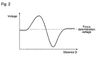
- Fig. 2 illustrates the S signal.
- the voltage value of the S signal changes according to a distance D between the optical head 10 and the work piece W.
- a determination is made that the optical head 10 (objective lens 14) is in the focal position with respect to the work piece W.
- the memory 52 stores programs and also various kinds of information.
- the S signal outputter 53 outputs the S signal to an exterior.
- the S signal outputter 53 converts a digital signal to an analog signal and outputs the signal.
- the S signal outputter 53 outputs serial or parallel digital signals, for example.
- the amplification rate of each of the amplifiers 21 and 22 is a fixed value in the comparative example.
- a value (AD value) digitized by the AD converter 40 is also small.
- an amount of change (sensitivity) of a calculated value of the S signal when the AD value is changed by 1 differs between cases where the AD value is small and cases where it is large.
- the calculated value of the S signal is 0.333.
- the calculated value of the S signal is 0.334. In this case, a difference in the S signal value before and after the change to the amplified signal B' is 0.001.
- the calculated value of the S signal is 0.333.
- the AD value of the amplified signal A' is 6 and the AD value of the amplified signal B' is similarly changed by only -1 to be 2
- the calculated value of the S signal is 0.5.
- the difference in the S signal value before and after the change to the amplified signal B' is 0.167. Accordingly, the S signal value relative to the change of -1 in the amplified signal B' changes more greatly when the low-reflectance work piece W is used than when the high-reflectance work piece W is used.
- the S signal value changes greatly with even a slight change to the signals A and B, and thus the S signal varies greatly due to electronic noise.
- the S signal is highly sensitive to changes in the signals A and B, and thus varies greatly. Similar detrimental effects occur even in a case where amplification is performed by switching between circuits having fixed amplification rates because there are cases where the AD value is small in a single amplification path.
- the amplification rate of each of the amplifiers 21 and 22 is defined based on voltage values Va and Vb of the amplified signals A' and B', respectively. Accordingly, even when the reflectance of the work piece W is low, the amplified signals A' and B' are not small and the AD value ordinarily obtained is a large value, in comparison to the comparative example. Therefore, variation in the S signal caused by electronic noise and sensitivity can be reduced more than in the comparative example. Accordingly, the present embodiment can increase the accuracy of identifying the focal position, in comparison to the comparative example.
- the second embodiment includes a maximum voltage detector 31a instead of the signal voltage adder 31.
- the second embodiment differs from the first embodiment in this respect.
- the maximum voltage detector 31 a detects the higher voltage value of the voltage value Va of the signal A' and the voltage value Vb of the signal B'.
- the amplification rate determiner 32 defines the amplification rate of each of the amplifiers 21 and 22 such that the detected higher voltage value is a constant voltage.
- the second embodiment having the above-described configuration achieves a similar effect to that of the first embodiment. Furthermore, in the first embodiment, there is a possibility that one of the amplified signals A' and B' may be larger than a range enabling digitization by the AD converter 40. Meanwhile, in the second embodiment, the amplified signals A' and B' can be kept within the range enabling digitization by the AD converter 40, using the above-noted configuration.
- the autofocus mechanism according to the present embodiment is a laser autofocus mechanism using a double knife-edge method.
- the autofocus mechanism includes an optical head 60, an amplifier 70, an amplification rate definer 80, an AD converter 90, and the computer 50.
- a light source (laser diode) 61 emits laser light, which traverses a tube lens 62 and a beam splitter 64 to pass through an objective lens 65, and is emitted at the work piece W.
- a beam of light that has passed through the objective lens 65 forms a light point image at the focal position of the objective lens 65.
- Fig. 4 illustrates an exemplary case where the focal position of the objective lens 65 is matched to the work piece W.
- the light reflected by the work piece W passes through the objective lens 65, is reflected by the beam splitter 64, passes through an auxiliary lens 63, and is guided to a triangular prism 66.
- a first portion forms a light point image on a halved sensor 67, which is configured by halved photoreceiver elements 67a and 67b.
- a second portion of the light forms a light point image on a halved sensor 68, which is configured by halved photoreceiver elements 68a and 68b.
- the light point image on the halved sensor 67 becomes blurry.
- the optical head 60 objective lens 65
- the amount of light received by the photoreceiver elements 67a and 68a increases.
- the optical head 60 is further away from the work piece W than is the focal position, the amount of light received by the photoreceiver elements 67b and 68b increases.
- the present embodiment can identify the focal position of the optical head 60 (objective lens 65) with respect to the work piece W. Moreover, the photoreceiver elements 67a and 67b output a signal C and a signal D, respectively, based on the amount of light received. The photoreceiver elements 68a and 68b output a signal E and a signal F, respectively, based on the amount of light received.
- the amplifier 70 includes an amplifier 71 for the signal C, an amplifier 72 for the signal D, an amplifier 73 for the signal E, and an amplifier 74 for the signal F.
- the amplifier 71 outputs an amplified signal C' (voltage value Vc), which is an amplification of the signal C, to a channel CH1 of the AD converter 90.
- the amplifier 72 outputs an amplified signal D' (voltage value Vd), which is an amplification of the signal D, to a channel CH2 of the AD converter 90.
- the amplifier 73 outputs an amplified signal E' (voltage value Ve), which is an amplification of the signal E, to a channel CH3 of the AD converter 90.
- the amplifier 74 outputs an amplified signal F' (voltage value Vf), which is an amplification of the signal F, to a channel CH4 of the AD converter 90.
- the amplification rate definer 80 includes a signal voltage adder 81 and an amplification rate determiner 82.
- the signal voltage adder 81 adds the voltage value Vc of the signal C', the voltage value Vd of the signal D', the voltage value Ve of the signal E', and the voltage value Vf of the signal F' (Vc + Vd + Ve + Vf).
- the amplification rate determiner 82 determines the amplification rate of each of the amplifiers 71 to 74 such that the added value Vc + Vd + Ve + Vf is a constant value.
- the amplification rate determiner 82 inputs amplification rate control signals Sc through Sf to the amplifiers 71 through 74, respectively, to control the amplification rate of each.
- the amplification rates of the amplifiers 71 to 74 are all the same.
- the amplification rate control signals Sc to Sf may be either one of analog signals and digital signals.
- the AD converter 90 converts the amplified signals C', D', E' and F' from analog signals into digital signals and outputs the converted signals to the computer 50.
- the third embodiment with the configuration described above, achieves a similar effect to that of the first embodiment.
- the present invention is not limited to these and can include various modifications, additions, and the like not deviating from the scope of the present invention.
- the double knife-edge method was applied to the first embodiment.
- the double knife-edge method according to the third embodiment can also be applied to the second embodiment, as well.
Landscapes
- Physics & Mathematics (AREA)
- General Physics & Mathematics (AREA)
- Optics & Photonics (AREA)
- Chemical & Material Sciences (AREA)
- Analytical Chemistry (AREA)
- Engineering & Computer Science (AREA)
- Computer Vision & Pattern Recognition (AREA)
- Automatic Focus Adjustment (AREA)
- Microscoopes, Condenser (AREA)
- Length Measuring Devices By Optical Means (AREA)
- Measurement Of Optical Distance (AREA)
Abstract
Description
- The present application claims priority under 35 U.S.C. §119 of Japanese Application No.
2013-138162, filed on July 1, 2013 - The present invention relates to an autofocus mechanism adjusting a focal position with respect to a work piece.
- Conventionally, an autofocus mechanism used in a measurement device is known (see Japanese Patent Laid-open Publication No.
H07-105547 - However, in a case where reflectance of the work piece is low, the amplified signals obtained in the autofocus mechanism are small. Thus, when electronic noise is present in the amplified signals, identification of the focal position becomes difficult. Specifically, accuracy of the autofocus is reduced. Moreover, feedback control, which tracks a surface of the work piece based on the focal position, cannot be performed stably.
- The present invention provides an autofocus mechanism with improved accuracy in identifying a focal position.
- An autofocus mechanism according to the present invention includes a light source emitting light through an objective lens at a work piece; a first detector detecting a portion of light reflected by the work piece and generating a first signal; a second detector detecting a portion of the reflected light and generating a second signal; a first amplifier amplifying the first signal and generating a first amplified signal; a second amplifier amplifying the second signal and generating a second amplified signal; an amplification rate definer defining an amplification rate of each of the first amplifier and the second amplifier based on the first amplified signal and the second amplified signal, respectively; and a calculator identifying a focal position of the objective lens based on the first amplified signal and the second amplified signal.
- According to the present invention, the amplification rate of each of the first amplifier and the second amplifier is defined based on the first amplified signal and the second amplified signal. Therefore, even when reflectance of the work piece is low, deterioration of the first and second amplified signals can be inhibited. The present invention thus provides an autofocus mechanism with improved accuracy in identifying a focal position.
- The present invention is further described in the detailed description which follows, in reference to the noted plurality of drawings by way of non-limiting examples of exemplary embodiments of the present invention, in which like reference numerals represent similar parts throughout the several views of the drawings, and wherein:
-
Fig. 1 is a schematic view illustrating a configuration of an autofocus mechanism according to a first embodiment; -
Fig. 2 illustrates an S signal; -
Fig. 3 is a schematic view illustrating a configuration of an autofocus mechanism according to a second embodiment; and -
Fig. 4 is a schematic view illustrating a configuration of an autofocus mechanism according to a third embodiment. - The particulars shown herein are by way of example and for purposes of illustrative discussion of the embodiments of the present invention only and are presented in the cause of providing what is believed to be the most useful and readily understood description of the principles and conceptual aspects of the present invention. In this regard, no attempt is made to show structural details of the present invention in more detail than is necessary for the fundamental understanding of the present invention, the description taken with the drawings making apparent to those skilled in the art how the forms of the present invention may be embodied in practice.
-
Fig. 1 is a schematic view illustrating a configuration of an autofocus mechanism according to a first embodiment. The autofocus mechanism according to the present embodiment is a laser autofocus mechanism using a so-called double pinhole method, and is installed in optical devices such as a microscope and an image measuring instrument, for example. - As shown in
Fig. 1 , the autofocus mechanism according to the present embodiment includes anoptical head 10, anamplifier 20, an amplification rate definer 30, anAD converter 40, and acomputer 50. Theoptical head 10 emits laser light at a work piece W, receives the light reflected by the work piece W, and converts the reflected light into an electric signal. Theamplifier 20 amplifies the electric signal received from theoptical head 10. The amplification rate definer 30 defines an amplification rate of theamplifier 20 based on the electric signal received from theamplifier 20. TheAD converter 40 converts the electric signal received from theamplifier 20 from an analog signal into a digital signal. Thecomputer 50 identifies a focal position based on the signal received from theAD converter 40. - As shown in
Fig. 1 , in theoptical head 10, a light source (laser diode) 11 emits laser light, which is emitted at abeam splitter 12a. Thebeam splitter 12a allows light from thelight source 11 to pass and bombard atube lens 13, and reflects the light reflected by the work piece W onto abeam splitter 12b. - The
tube lens 13 converts the light from thebeam splitter 12a into parallel light, which is emitted through anobjective lens 14 at the work piece W. In addition, thetube lens 13 allows the light reflected by the work piece W to bombard thebeam splitter 12a. Thebeam splitter 12b scatters the light from thebeam splitter 12a and allows transmitted light to bombard, through apinhole 15a, a photoreceiver element (photodiode) 16a. In addition, thebeam splitter 12b allows reflected light to bombard, through apinhole 15b, a photoreceiver element (photodiode) 16b. Thephotoreceiver elements amplifier 20 based on an amount of light received. - In
Fig. 1 , when the optical head 10 (objective lens 14) is arranged in the focal position with respect to the work piece W, output of thephotoreceiver elements optical head 10 is arranged so as to be further away from the work piece W than is the focal position, the output of thephotoreceiver element 16b is greater than the output of thephotoreceiver element 16a. Meanwhile, when theoptical head 10 is arranged so as to be closer to the work piece W than is the focal position, the output of thephotoreceiver element 16b is less than the output of thephotoreceiver element 16a. Making use of such changes, the present embodiment can identify the focal position of the optical head 10 (objective lens 14) with respect to the work piece W. - As shown in
Fig. 1 , theamplifier 20 includes anamplifier 21 for the signal A and anamplifier 22 for the signal B. Theamplifier 21 outputs an amplified signal A' (voltage value Va), which is an amplification of the signal A, to a channel CH1 of theAD converter 40. Theamplifier 22 outputs an amplified signal B' (voltage value Vb), which is an amplification of the signal B, to a channel CH2 of theAD converter 40. - As shown in
Fig. 1 , the amplification rate definer 30 includes asignal voltage adder 31 and an amplification rate determiner 32. Thesignal voltage adder 31 adds the voltage value Va of the signal A' and the voltage value Vb of the signal B' (Va + Vb). The amplification rate determiner 32 determines the amplification rate of each of theamplifiers amplifiers amplifiers - The
AD converter 40 converts the amplified signals A' and B' from analog signals into digital signals and outputs the converted signals to thecomputer 50. - As shown in
Fig. 1 , thecomputer 50 includes acalculator 51, amemory 52, and anS signal outputter 53. Thecalculator 51 calculates the S signal based on the signals A' and B' input from theAD converter 40. Herein, the S signal is a signal identifying the focal position of theobjective lens 14 with respect to the work piece W. Specifically, the S signal is calculated based on [S signal = (A' - B') ÷ (A' + B')].Fig. 2 illustrates the S signal. As shown inFig. 2 , the voltage value of the S signal changes according to a distance D between theoptical head 10 and the work piece W. In addition, when the voltage value of the S signal matches a focus determination voltage, a determination is made that the optical head 10 (objective lens 14) is in the focal position with respect to the work piece W. - The
memory 52 stores programs and also various kinds of information. TheS signal outputter 53 outputs the S signal to an exterior. For example, theS signal outputter 53 converts a digital signal to an analog signal and outputs the signal. Further, theS signal outputter 53 outputs serial or parallel digital signals, for example. - Next, an advantage of the present embodiment is described in comparison to a comparative example. The amplification rate of each of the
amplifiers AD converter 40 is also small. In an S signal calculation formula, an amount of change (sensitivity) of a calculated value of the S signal when the AD value is changed by 1 differs between cases where the AD value is small and cases where it is large. - For example, in a case where the AD value of the amplified signal A' is 600 and the AD value of the amplified signal B' is 300 with a high-reflectance work piece W, the calculated value of the S signal is 0.333. Further, in a case where the AD value of the amplified signal A' is 600 and the AD value of the amplified signal B' is changed by only -1 to be 299, the calculated value of the S signal is 0.334. In this case, a difference in the S signal value before and after the change to the amplified signal B' is 0.001.
- Meanwhile, in a case where the AD value of the amplified signal A' is 6 and the AD value of the amplified signal B' is 3 with a low-reflectance work piece W, the calculated value of the S signal is 0.333. Further, in a case where the AD value of the amplified signal A' is 6 and the AD value of the amplified signal B' is similarly changed by only -1 to be 2, the calculated value of the S signal is 0.5. In this case, the difference in the S signal value before and after the change to the amplified signal B' is 0.167. Accordingly, the S signal value relative to the change of -1 in the amplified signal B' changes more greatly when the low-reflectance work piece W is used than when the high-reflectance work piece W is used.
- As noted above, with the low-reflectance work piece W, the S signal value changes greatly with even a slight change to the signals A and B, and thus the S signal varies greatly due to electronic noise. Alternatively, the S signal is highly sensitive to changes in the signals A and B, and thus varies greatly. Similar detrimental effects occur even in a case where amplification is performed by switching between circuits having fixed amplification rates because there are cases where the AD value is small in a single amplification path.
- In contrast, in the present embodiment, the amplification rate of each of the
amplifiers - Next, an autofocus mechanism according to a second embodiment is described with reference to
Fig. 3 . As shown inFig. 3 , the second embodiment includes amaximum voltage detector 31a instead of thesignal voltage adder 31. The second embodiment differs from the first embodiment in this respect. - The
maximum voltage detector 31 a detects the higher voltage value of the voltage value Va of the signal A' and the voltage value Vb of the signal B'. Theamplification rate determiner 32 defines the amplification rate of each of theamplifiers - The second embodiment having the above-described configuration achieves a similar effect to that of the first embodiment. Furthermore, in the first embodiment, there is a possibility that one of the amplified signals A' and B' may be larger than a range enabling digitization by the
AD converter 40. Meanwhile, in the second embodiment, the amplified signals A' and B' can be kept within the range enabling digitization by theAD converter 40, using the above-noted configuration. - Next, an autofocus mechanism according to a third embodiment is described with reference to
Fig. 4 . The autofocus mechanism according to the present embodiment is a laser autofocus mechanism using a double knife-edge method. - As shown in
Fig. 4 , the autofocus mechanism according to the present embodiment includes anoptical head 60, anamplifier 70, anamplification rate definer 80, anAD converter 90, and thecomputer 50. - As shown in
Fig. 4 , in theoptical head 60, a light source (laser diode) 61 emits laser light, which traverses atube lens 62 and abeam splitter 64 to pass through anobjective lens 65, and is emitted at the work piece W. A beam of light that has passed through theobjective lens 65 forms a light point image at the focal position of theobjective lens 65.Fig. 4 illustrates an exemplary case where the focal position of theobjective lens 65 is matched to the work piece W. The light reflected by the work piece W passes through theobjective lens 65, is reflected by thebeam splitter 64, passes through anauxiliary lens 63, and is guided to atriangular prism 66. - Of the light split by the
triangular prism 66, a first portion forms a light point image on a halvedsensor 67, which is configured by halved photoreceiver elements 67a and 67b. A second portion of the light forms a light point image on a halvedsensor 68, which is configured by halvedphotoreceiver elements - In the present embodiment, when relative positions of the work piece W and the
optical head 60 change in an optical axis direction of theobjective lens 65 and the work piece W deviates from the focal position of theobjective lens 65, the light point image on the halvedsensor 67 becomes blurry. When the optical head 60 (objective lens 65) is closer to the work piece W than is the focal position, the amount of light received by thephotoreceiver elements 67a and 68a increases. Meanwhile, when the optical head 60 (objective lens 65) is further away from the work piece W than is the focal position, the amount of light received by thephotoreceiver elements 67b and 68b increases. Making use of such changes, the present embodiment can identify the focal position of the optical head 60 (objective lens 65) with respect to the work piece W. Moreover, the photoreceiver elements 67a and 67b output a signal C and a signal D, respectively, based on the amount of light received. Thephotoreceiver elements - As shown in
Fig. 4 , theamplifier 70 includes anamplifier 71 for the signal C, anamplifier 72 for the signal D, anamplifier 73 for the signal E, and anamplifier 74 for the signal F. - The
amplifier 71 outputs an amplified signal C' (voltage value Vc), which is an amplification of the signal C, to a channel CH1 of theAD converter 90. Theamplifier 72 outputs an amplified signal D' (voltage value Vd), which is an amplification of the signal D, to a channel CH2 of theAD converter 90. Theamplifier 73 outputs an amplified signal E' (voltage value Ve), which is an amplification of the signal E, to a channel CH3 of theAD converter 90. Theamplifier 74 outputs an amplified signal F' (voltage value Vf), which is an amplification of the signal F, to a channel CH4 of theAD converter 90. - As shown in
Fig. 4 , theamplification rate definer 80 includes asignal voltage adder 81 and anamplification rate determiner 82. Thesignal voltage adder 81 adds the voltage value Vc of the signal C', the voltage value Vd of the signal D', the voltage value Ve of the signal E', and the voltage value Vf of the signal F' (Vc + Vd + Ve + Vf). Theamplification rate determiner 82 determines the amplification rate of each of theamplifiers 71 to 74 such that the added value Vc + Vd + Ve + Vf is a constant value. Specifically, theamplification rate determiner 82 inputs amplification rate control signals Sc through Sf to theamplifiers 71 through 74, respectively, to control the amplification rate of each. The amplification rates of theamplifiers 71 to 74 are all the same. Moreover, the amplification rate control signals Sc to Sf may be either one of analog signals and digital signals. - The
AD converter 90 converts the amplified signals C', D', E' and F' from analog signals into digital signals and outputs the converted signals to thecomputer 50. - The
computer 50 has a configuration substantially similar to that of the first embodiment. However, calculation of the S signal by thecalculator 51 according to the third embodiment is different from that of the first embodiment. Specifically, the S signal is calculated based on [S signal = (C' - D') (C' + D') + (E' - F') ÷ (E' + F')]. The third embodiment, with the configuration described above, achieves a similar effect to that of the first embodiment. - Embodiments of the present invention were described above, but the present invention is not limited to these and can include various modifications, additions, and the like not deviating from the scope of the present invention. For example, in the third embodiment, the double knife-edge method was applied to the first embodiment. However, the double knife-edge method according to the third embodiment can also be applied to the second embodiment, as well.
- It is noted that the foregoing examples have been provided merely for the purpose of explanation and are in no way to be construed as limiting of the present invention. While the present invention has been described with reference to exemplary embodiments, it is understood that the words which have been used herein are words of description and illustration, rather than words of limitation. Changes may be made, within the purview of the appended claims, as presently stated and as amended, without departing from the scope and spirit of the present invention in its aspects. Although the present invention has been described herein with reference to particular structures, materials and embodiments, the present invention is not intended to be limited to the particulars disclosed herein; rather, the present invention extends to all functionally equivalent structures, methods and uses, such as are within the scope of the appended claims.
- The present invention is not limited to the above described embodiments, and various variations and modifications may be possible without departing from the scope of the present invention.
- Features, components and specific details of the structures of the above-described embodiments may be exchanged or combined to form further embodiments optimized for the respective application. As far as those modifications are readily apparent for an expert skilled in the art they shall be disclosed implicitly by the above description without specifying explicitly every possible combination, for the sake of conciseness of the present description.
Claims (3)
- An autofocus mechanism comprising:a light source (11) configured to emit light through an objective lens (14) onto a work piece (W);a first detector (16b) configured to detect a first portion of the light reflected by the work piece (W) and generate a first signal (A);a second detector (16a) configured to detect a second portion of the reflected light and generate a second signal (B);a first amplifier (21) configured to amplify the first signal (A) and generate a first amplified signal (A');a second amplifier (22) configured to amplify the second signal (B) and generate a second amplified signal (B');an amplification rate definer (30) configured to define an amplification rate of each of the first amplifier (21) and the second amplifier (22) based on the first amplified signal (A') and the second amplified signal (B'), respectively; anda calculator (51) configured to identify a focal position of the objective lens (14) based on the first amplified signal (A') and the second amplified signal (B').
- The autofocus mechanism according to claim 1, wherein the amplification rate definer (30) is further configured to define the amplification rate of each of the first amplifier (21) and the second amplifier (22) such that a total of a voltage value (Va) of the first amplified signal (A') and the voltage value (Vb) of the second amplified signal (B') is a constant value.
- The autofocus mechanism according to claim 1 or 2, wherein the amplification rate definer (30) is further configured to define the amplification rate of each of the first amplifier (21) and the second amplifier (22) such that the signal having a higher voltage, of the first amplified signal (A') and the second amplified signal (B'), has a constant voltage.
Applications Claiming Priority (1)
| Application Number | Priority Date | Filing Date | Title |
|---|---|---|---|
| JP2013138162A JP6336718B2 (en) | 2013-07-01 | 2013-07-01 | Autofocus device |
Publications (2)
| Publication Number | Publication Date |
|---|---|
| EP2821837A1 true EP2821837A1 (en) | 2015-01-07 |
| EP2821837B1 EP2821837B1 (en) | 2020-10-14 |
Family
ID=51033012
Family Applications (1)
| Application Number | Title | Priority Date | Filing Date |
|---|---|---|---|
| EP14174933.3A Not-in-force EP2821837B1 (en) | 2013-07-01 | 2014-06-30 | Autofocus mechanism |
Country Status (3)
| Country | Link |
|---|---|
| US (1) | US9638911B2 (en) |
| EP (1) | EP2821837B1 (en) |
| JP (1) | JP6336718B2 (en) |
Cited By (1)
| Publication number | Priority date | Publication date | Assignee | Title |
|---|---|---|---|---|
| US11284060B2 (en) | 2018-01-31 | 2022-03-22 | Japan Display Inc. | Display device and display system |
Families Citing this family (2)
| Publication number | Priority date | Publication date | Assignee | Title |
|---|---|---|---|---|
| JP2016071010A (en) | 2014-09-29 | 2016-05-09 | 株式会社ミツトヨ | Autofocus device, autofocus method, and program |
| EP3418789A1 (en) * | 2017-06-20 | 2018-12-26 | Euroimmun Medizinische Labordiagnostika AG | Method and microscope system for recording an image |
Citations (3)
| Publication number | Priority date | Publication date | Assignee | Title |
|---|---|---|---|---|
| US4311904A (en) * | 1978-12-05 | 1982-01-19 | Nippon Kogaku K.K. | Automatic focus adjusting device |
| US4625103A (en) * | 1982-11-30 | 1986-11-25 | Asahi Kogaku Kogyo Kabushiki Kaisha | Automatic focusing device in microscope system |
| JPH07105547A (en) | 1993-10-01 | 1995-04-21 | Mitsutoyo Corp | Automatic focusing mechanism |
Family Cites Families (6)
| Publication number | Priority date | Publication date | Assignee | Title |
|---|---|---|---|---|
| US5471046A (en) * | 1994-02-25 | 1995-11-28 | Eastman Kodak Company | Camera auto-focusing system with designator using a volume holographic element |
| JPH11337812A (en) * | 1998-05-21 | 1999-12-10 | Olympus Optical Co Ltd | Autofocus device |
| JP2001013005A (en) * | 1999-07-01 | 2001-01-19 | Keyence Corp | Light quantity detecting circuit capable of controlling photoelectric conversion ratio |
| US7297921B2 (en) * | 2003-11-21 | 2007-11-20 | Olympus Corportion | Photodetection circuit and confocal microscope that has it |
| US7514661B2 (en) * | 2005-01-04 | 2009-04-07 | Hewlett-Packard Development Company, L.P. | Focus calibration in an optical drive |
| JP5732265B2 (en) * | 2011-01-24 | 2015-06-10 | 株式会社キーエンス | Microscope system, focus position detection method, and focus position detection program |
-
2013
- 2013-07-01 JP JP2013138162A patent/JP6336718B2/en not_active Expired - Fee Related
-
2014
- 2014-06-26 US US14/315,826 patent/US9638911B2/en not_active Expired - Fee Related
- 2014-06-30 EP EP14174933.3A patent/EP2821837B1/en not_active Not-in-force
Patent Citations (3)
| Publication number | Priority date | Publication date | Assignee | Title |
|---|---|---|---|---|
| US4311904A (en) * | 1978-12-05 | 1982-01-19 | Nippon Kogaku K.K. | Automatic focus adjusting device |
| US4625103A (en) * | 1982-11-30 | 1986-11-25 | Asahi Kogaku Kogyo Kabushiki Kaisha | Automatic focusing device in microscope system |
| JPH07105547A (en) | 1993-10-01 | 1995-04-21 | Mitsutoyo Corp | Automatic focusing mechanism |
Cited By (1)
| Publication number | Priority date | Publication date | Assignee | Title |
|---|---|---|---|---|
| US11284060B2 (en) | 2018-01-31 | 2022-03-22 | Japan Display Inc. | Display device and display system |
Also Published As
| Publication number | Publication date |
|---|---|
| US9638911B2 (en) | 2017-05-02 |
| EP2821837B1 (en) | 2020-10-14 |
| JP2015011275A (en) | 2015-01-19 |
| US20150001373A1 (en) | 2015-01-01 |
| JP6336718B2 (en) | 2018-06-06 |
Similar Documents
| Publication | Publication Date | Title |
|---|---|---|
| US20020075588A1 (en) | Tape edge monitoring | |
| US9638911B2 (en) | Autofocus mechanism | |
| EP3153878A1 (en) | Distance-settable photoelectric sensor | |
| EP2180301A3 (en) | Wavelength shift measuring apparatus, optical source apparatus, interference measuring apparatus, exposure apparatus, and device manufacturing method | |
| WO2019027253A3 (en) | Catheter for sensing pressure applied to front end thereof by using optical fiber and catheter system therefor | |
| US20060092428A1 (en) | Position measuring system | |
| KR102590280B1 (en) | apparatus for measuring distribution temperature by using optical fiber and method of correction temperature thereof | |
| JP4979916B2 (en) | Surveying device and surveying method | |
| TWI667464B (en) | Optical measurement device and optical measurement method | |
| US9341812B2 (en) | Autofocus mechanism with a first and second amplification rate | |
| KR20210077738A (en) | Optical measuring device and optical measuring method | |
| EP3543645B1 (en) | Optical measurement device and optical measurement method | |
| ATE510282T1 (en) | MEASURING DEVICE | |
| KR102113079B1 (en) | Thickness measuring device | |
| JPH11337812A (en) | Autofocus device | |
| JP2010266364A (en) | Laser displacement meter | |
| EP2151666A1 (en) | Length measuring apparatus | |
| JP6907064B2 (en) | Displacement detector | |
| WO2020145172A1 (en) | Optical measurement device and optical measurement method |
Legal Events
| Date | Code | Title | Description |
|---|---|---|---|
| PUAI | Public reference made under article 153(3) epc to a published international application that has entered the european phase |
Free format text: ORIGINAL CODE: 0009012 |
|
| 17P | Request for examination filed |
Effective date: 20140630 |
|
| AK | Designated contracting states |
Kind code of ref document: A1 Designated state(s): AL AT BE BG CH CY CZ DE DK EE ES FI FR GB GR HR HU IE IS IT LI LT LU LV MC MK MT NL NO PL PT RO RS SE SI SK SM TR |
|
| AX | Request for extension of the european patent |
Extension state: BA ME |
|
| R17P | Request for examination filed (corrected) |
Effective date: 20150707 |
|
| RBV | Designated contracting states (corrected) |
Designated state(s): AL AT BE BG CH CY CZ DE DK EE ES FI FR GB GR HR HU IE IS IT LI LT LU LV MC MK MT NL NO PL PT RO RS SE SI SK SM TR |
|
| STAA | Information on the status of an ep patent application or granted ep patent |
Free format text: STATUS: EXAMINATION IS IN PROGRESS |
|
| 17Q | First examination report despatched |
Effective date: 20181004 |
|
| GRAP | Despatch of communication of intention to grant a patent |
Free format text: ORIGINAL CODE: EPIDOSNIGR1 |
|
| STAA | Information on the status of an ep patent application or granted ep patent |
Free format text: STATUS: GRANT OF PATENT IS INTENDED |
|
| RIC1 | Information provided on ipc code assigned before grant |
Ipc: G02B 7/38 20060101ALN20200403BHEP Ipc: G02B 21/24 20060101AFI20200403BHEP |
|
| INTG | Intention to grant announced |
Effective date: 20200429 |
|
| RIN1 | Information on inventor provided before grant (corrected) |
Inventor name: UDO, SHOHEI |
|
| GRAS | Grant fee paid |
Free format text: ORIGINAL CODE: EPIDOSNIGR3 |
|
| GRAA | (expected) grant |
Free format text: ORIGINAL CODE: 0009210 |
|
| STAA | Information on the status of an ep patent application or granted ep patent |
Free format text: STATUS: THE PATENT HAS BEEN GRANTED |
|
| AK | Designated contracting states |
Kind code of ref document: B1 Designated state(s): AL AT BE BG CH CY CZ DE DK EE ES FI FR GB GR HR HU IE IS IT LI LT LU LV MC MK MT NL NO PL PT RO RS SE SI SK SM TR |
|
| REG | Reference to a national code |
Ref country code: GB Ref legal event code: FG4D |
|
| REG | Reference to a national code |
Ref country code: AT Ref legal event code: REF Ref document number: 1324149 Country of ref document: AT Kind code of ref document: T Effective date: 20201015 Ref country code: CH Ref legal event code: EP |
|
| REG | Reference to a national code |
Ref country code: DE Ref legal event code: R096 Ref document number: 602014071168 Country of ref document: DE |
|
| REG | Reference to a national code |
Ref country code: IE Ref legal event code: FG4D |
|
| REG | Reference to a national code |
Ref country code: AT Ref legal event code: MK05 Ref document number: 1324149 Country of ref document: AT Kind code of ref document: T Effective date: 20201014 |
|
| REG | Reference to a national code |
Ref country code: NL Ref legal event code: MP Effective date: 20201014 |
|
| PG25 | Lapsed in a contracting state [announced via postgrant information from national office to epo] |
Ref country code: GR Free format text: LAPSE BECAUSE OF FAILURE TO SUBMIT A TRANSLATION OF THE DESCRIPTION OR TO PAY THE FEE WITHIN THE PRESCRIBED TIME-LIMIT Effective date: 20210115 Ref country code: FI Free format text: LAPSE BECAUSE OF FAILURE TO SUBMIT A TRANSLATION OF THE DESCRIPTION OR TO PAY THE FEE WITHIN THE PRESCRIBED TIME-LIMIT Effective date: 20201014 Ref country code: RS Free format text: LAPSE BECAUSE OF FAILURE TO SUBMIT A TRANSLATION OF THE DESCRIPTION OR TO PAY THE FEE WITHIN THE PRESCRIBED TIME-LIMIT Effective date: 20201014 Ref country code: PT Free format text: LAPSE BECAUSE OF FAILURE TO SUBMIT A TRANSLATION OF THE DESCRIPTION OR TO PAY THE FEE WITHIN THE PRESCRIBED TIME-LIMIT Effective date: 20210215 Ref country code: NL Free format text: LAPSE BECAUSE OF FAILURE TO SUBMIT A TRANSLATION OF THE DESCRIPTION OR TO PAY THE FEE WITHIN THE PRESCRIBED TIME-LIMIT Effective date: 20201014 Ref country code: NO Free format text: LAPSE BECAUSE OF FAILURE TO SUBMIT A TRANSLATION OF THE DESCRIPTION OR TO PAY THE FEE WITHIN THE PRESCRIBED TIME-LIMIT Effective date: 20210114 |
|
| REG | Reference to a national code |
Ref country code: LT Ref legal event code: MG4D |
|
| PG25 | Lapsed in a contracting state [announced via postgrant information from national office to epo] |
Ref country code: BG Free format text: LAPSE BECAUSE OF FAILURE TO SUBMIT A TRANSLATION OF THE DESCRIPTION OR TO PAY THE FEE WITHIN THE PRESCRIBED TIME-LIMIT Effective date: 20210114 Ref country code: ES Free format text: LAPSE BECAUSE OF FAILURE TO SUBMIT A TRANSLATION OF THE DESCRIPTION OR TO PAY THE FEE WITHIN THE PRESCRIBED TIME-LIMIT Effective date: 20201014 Ref country code: AT Free format text: LAPSE BECAUSE OF FAILURE TO SUBMIT A TRANSLATION OF THE DESCRIPTION OR TO PAY THE FEE WITHIN THE PRESCRIBED TIME-LIMIT Effective date: 20201014 Ref country code: SE Free format text: LAPSE BECAUSE OF FAILURE TO SUBMIT A TRANSLATION OF THE DESCRIPTION OR TO PAY THE FEE WITHIN THE PRESCRIBED TIME-LIMIT Effective date: 20201014 Ref country code: IS Free format text: LAPSE BECAUSE OF FAILURE TO SUBMIT A TRANSLATION OF THE DESCRIPTION OR TO PAY THE FEE WITHIN THE PRESCRIBED TIME-LIMIT Effective date: 20210214 Ref country code: LV Free format text: LAPSE BECAUSE OF FAILURE TO SUBMIT A TRANSLATION OF THE DESCRIPTION OR TO PAY THE FEE WITHIN THE PRESCRIBED TIME-LIMIT Effective date: 20201014 Ref country code: PL Free format text: LAPSE BECAUSE OF FAILURE TO SUBMIT A TRANSLATION OF THE DESCRIPTION OR TO PAY THE FEE WITHIN THE PRESCRIBED TIME-LIMIT Effective date: 20201014 |
|
| PG25 | Lapsed in a contracting state [announced via postgrant information from national office to epo] |
Ref country code: HR Free format text: LAPSE BECAUSE OF FAILURE TO SUBMIT A TRANSLATION OF THE DESCRIPTION OR TO PAY THE FEE WITHIN THE PRESCRIBED TIME-LIMIT Effective date: 20201014 |
|
| REG | Reference to a national code |
Ref country code: DE Ref legal event code: R097 Ref document number: 602014071168 Country of ref document: DE |
|
| PG25 | Lapsed in a contracting state [announced via postgrant information from national office to epo] |
Ref country code: LT Free format text: LAPSE BECAUSE OF FAILURE TO SUBMIT A TRANSLATION OF THE DESCRIPTION OR TO PAY THE FEE WITHIN THE PRESCRIBED TIME-LIMIT Effective date: 20201014 Ref country code: SK Free format text: LAPSE BECAUSE OF FAILURE TO SUBMIT A TRANSLATION OF THE DESCRIPTION OR TO PAY THE FEE WITHIN THE PRESCRIBED TIME-LIMIT Effective date: 20201014 Ref country code: RO Free format text: LAPSE BECAUSE OF FAILURE TO SUBMIT A TRANSLATION OF THE DESCRIPTION OR TO PAY THE FEE WITHIN THE PRESCRIBED TIME-LIMIT Effective date: 20201014 Ref country code: EE Free format text: LAPSE BECAUSE OF FAILURE TO SUBMIT A TRANSLATION OF THE DESCRIPTION OR TO PAY THE FEE WITHIN THE PRESCRIBED TIME-LIMIT Effective date: 20201014 Ref country code: CZ Free format text: LAPSE BECAUSE OF FAILURE TO SUBMIT A TRANSLATION OF THE DESCRIPTION OR TO PAY THE FEE WITHIN THE PRESCRIBED TIME-LIMIT Effective date: 20201014 Ref country code: SM Free format text: LAPSE BECAUSE OF FAILURE TO SUBMIT A TRANSLATION OF THE DESCRIPTION OR TO PAY THE FEE WITHIN THE PRESCRIBED TIME-LIMIT Effective date: 20201014 |
|
| PLBE | No opposition filed within time limit |
Free format text: ORIGINAL CODE: 0009261 |
|
| STAA | Information on the status of an ep patent application or granted ep patent |
Free format text: STATUS: NO OPPOSITION FILED WITHIN TIME LIMIT |
|
| PG25 | Lapsed in a contracting state [announced via postgrant information from national office to epo] |
Ref country code: DK Free format text: LAPSE BECAUSE OF FAILURE TO SUBMIT A TRANSLATION OF THE DESCRIPTION OR TO PAY THE FEE WITHIN THE PRESCRIBED TIME-LIMIT Effective date: 20201014 |
|
| 26N | No opposition filed |
Effective date: 20210715 |
|
| PG25 | Lapsed in a contracting state [announced via postgrant information from national office to epo] |
Ref country code: AL Free format text: LAPSE BECAUSE OF FAILURE TO SUBMIT A TRANSLATION OF THE DESCRIPTION OR TO PAY THE FEE WITHIN THE PRESCRIBED TIME-LIMIT Effective date: 20201014 Ref country code: IT Free format text: LAPSE BECAUSE OF FAILURE TO SUBMIT A TRANSLATION OF THE DESCRIPTION OR TO PAY THE FEE WITHIN THE PRESCRIBED TIME-LIMIT Effective date: 20201014 |
|
| PG25 | Lapsed in a contracting state [announced via postgrant information from national office to epo] |
Ref country code: SI Free format text: LAPSE BECAUSE OF FAILURE TO SUBMIT A TRANSLATION OF THE DESCRIPTION OR TO PAY THE FEE WITHIN THE PRESCRIBED TIME-LIMIT Effective date: 20201014 |
|
| PG25 | Lapsed in a contracting state [announced via postgrant information from national office to epo] |
Ref country code: MC Free format text: LAPSE BECAUSE OF FAILURE TO SUBMIT A TRANSLATION OF THE DESCRIPTION OR TO PAY THE FEE WITHIN THE PRESCRIBED TIME-LIMIT Effective date: 20201014 |
|
| REG | Reference to a national code |
Ref country code: CH Ref legal event code: PL |
|
| REG | Reference to a national code |
Ref country code: BE Ref legal event code: MM Effective date: 20210630 |
|
| PG25 | Lapsed in a contracting state [announced via postgrant information from national office to epo] |
Ref country code: LU Free format text: LAPSE BECAUSE OF NON-PAYMENT OF DUE FEES Effective date: 20210630 |
|
| PG25 | Lapsed in a contracting state [announced via postgrant information from national office to epo] |
Ref country code: LI Free format text: LAPSE BECAUSE OF NON-PAYMENT OF DUE FEES Effective date: 20210630 Ref country code: IE Free format text: LAPSE BECAUSE OF NON-PAYMENT OF DUE FEES Effective date: 20210630 Ref country code: CH Free format text: LAPSE BECAUSE OF NON-PAYMENT OF DUE FEES Effective date: 20210630 |
|
| PG25 | Lapsed in a contracting state [announced via postgrant information from national office to epo] |
Ref country code: IS Free format text: LAPSE BECAUSE OF FAILURE TO SUBMIT A TRANSLATION OF THE DESCRIPTION OR TO PAY THE FEE WITHIN THE PRESCRIBED TIME-LIMIT Effective date: 20210214 Ref country code: FR Free format text: LAPSE BECAUSE OF NON-PAYMENT OF DUE FEES Effective date: 20210630 |
|
| PG25 | Lapsed in a contracting state [announced via postgrant information from national office to epo] |
Ref country code: BE Free format text: LAPSE BECAUSE OF NON-PAYMENT OF DUE FEES Effective date: 20210630 |
|
| PG25 | Lapsed in a contracting state [announced via postgrant information from national office to epo] |
Ref country code: HU Free format text: LAPSE BECAUSE OF FAILURE TO SUBMIT A TRANSLATION OF THE DESCRIPTION OR TO PAY THE FEE WITHIN THE PRESCRIBED TIME-LIMIT; INVALID AB INITIO Effective date: 20140630 |
|
| PG25 | Lapsed in a contracting state [announced via postgrant information from national office to epo] |
Ref country code: CY Free format text: LAPSE BECAUSE OF FAILURE TO SUBMIT A TRANSLATION OF THE DESCRIPTION OR TO PAY THE FEE WITHIN THE PRESCRIBED TIME-LIMIT Effective date: 20201014 |
|
| PGFP | Annual fee paid to national office [announced via postgrant information from national office to epo] |
Ref country code: DE Payment date: 20230620 Year of fee payment: 10 |
|
| PGFP | Annual fee paid to national office [announced via postgrant information from national office to epo] |
Ref country code: GB Payment date: 20230622 Year of fee payment: 10 |
|
| PG25 | Lapsed in a contracting state [announced via postgrant information from national office to epo] |
Ref country code: MK Free format text: LAPSE BECAUSE OF FAILURE TO SUBMIT A TRANSLATION OF THE DESCRIPTION OR TO PAY THE FEE WITHIN THE PRESCRIBED TIME-LIMIT Effective date: 20201014 |
|
| PG25 | Lapsed in a contracting state [announced via postgrant information from national office to epo] |
Ref country code: MT Free format text: LAPSE BECAUSE OF FAILURE TO SUBMIT A TRANSLATION OF THE DESCRIPTION OR TO PAY THE FEE WITHIN THE PRESCRIBED TIME-LIMIT Effective date: 20201014 |
|
| REG | Reference to a national code |
Ref country code: DE Ref legal event code: R119 Ref document number: 602014071168 Country of ref document: DE |
|
| GBPC | Gb: european patent ceased through non-payment of renewal fee |
Effective date: 20240630 |
|
| PG25 | Lapsed in a contracting state [announced via postgrant information from national office to epo] |
Ref country code: DE Free format text: LAPSE BECAUSE OF NON-PAYMENT OF DUE FEES Effective date: 20250101 |
|
| PG25 | Lapsed in a contracting state [announced via postgrant information from national office to epo] |
Ref country code: GB Free format text: LAPSE BECAUSE OF NON-PAYMENT OF DUE FEES Effective date: 20240630 |
|
| PG25 | Lapsed in a contracting state [announced via postgrant information from national office to epo] |
Ref country code: TR Free format text: LAPSE BECAUSE OF FAILURE TO SUBMIT A TRANSLATION OF THE DESCRIPTION OR TO PAY THE FEE WITHIN THE PRESCRIBED TIME-LIMIT Effective date: 20201014 |