EP2819203A2 - Organic light-emitting display apparatus and method of manufacturing the same - Google Patents
Organic light-emitting display apparatus and method of manufacturing the same Download PDFInfo
- Publication number
- EP2819203A2 EP2819203A2 EP14174847.5A EP14174847A EP2819203A2 EP 2819203 A2 EP2819203 A2 EP 2819203A2 EP 14174847 A EP14174847 A EP 14174847A EP 2819203 A2 EP2819203 A2 EP 2819203A2
- Authority
- EP
- European Patent Office
- Prior art keywords
- layer
- insulating layer
- penetration
- organic light
- display apparatus
- Prior art date
- Legal status (The legal status is an assumption and is not a legal conclusion. Google has not performed a legal analysis and makes no representation as to the accuracy of the status listed.)
- Granted
Links
Images



Classifications
-
- H—ELECTRICITY
- H10—SEMICONDUCTOR DEVICES; ELECTRIC SOLID-STATE DEVICES NOT OTHERWISE PROVIDED FOR
- H10K—ORGANIC ELECTRIC SOLID-STATE DEVICES
- H10K59/00—Integrated devices, or assemblies of multiple devices, comprising at least one organic light-emitting element covered by group H10K50/00
- H10K59/10—OLED displays
- H10K59/12—Active-matrix OLED [AMOLED] displays
- H10K59/131—Interconnections, e.g. wiring lines or terminals
-
- H—ELECTRICITY
- H10—SEMICONDUCTOR DEVICES; ELECTRIC SOLID-STATE DEVICES NOT OTHERWISE PROVIDED FOR
- H10K—ORGANIC ELECTRIC SOLID-STATE DEVICES
- H10K50/00—Organic light-emitting devices
- H10K50/80—Constructional details
- H10K50/84—Passivation; Containers; Encapsulations
- H10K50/842—Containers
- H10K50/8426—Peripheral sealing arrangements, e.g. adhesives, sealants
-
- H—ELECTRICITY
- H10—SEMICONDUCTOR DEVICES; ELECTRIC SOLID-STATE DEVICES NOT OTHERWISE PROVIDED FOR
- H10K—ORGANIC ELECTRIC SOLID-STATE DEVICES
- H10K59/00—Integrated devices, or assemblies of multiple devices, comprising at least one organic light-emitting element covered by group H10K50/00
- H10K59/10—OLED displays
- H10K59/12—Active-matrix OLED [AMOLED] displays
-
- H—ELECTRICITY
- H10—SEMICONDUCTOR DEVICES; ELECTRIC SOLID-STATE DEVICES NOT OTHERWISE PROVIDED FOR
- H10K—ORGANIC ELECTRIC SOLID-STATE DEVICES
- H10K59/00—Integrated devices, or assemblies of multiple devices, comprising at least one organic light-emitting element covered by group H10K50/00
- H10K59/80—Constructional details
- H10K59/87—Passivation; Containers; Encapsulations
- H10K59/871—Self-supporting sealing arrangements
- H10K59/8722—Peripheral sealing arrangements, e.g. adhesives, sealants
-
- H—ELECTRICITY
- H10—SEMICONDUCTOR DEVICES; ELECTRIC SOLID-STATE DEVICES NOT OTHERWISE PROVIDED FOR
- H10K—ORGANIC ELECTRIC SOLID-STATE DEVICES
- H10K59/00—Integrated devices, or assemblies of multiple devices, comprising at least one organic light-emitting element covered by group H10K50/00
- H10K59/10—OLED displays
- H10K59/12—Active-matrix OLED [AMOLED] displays
- H10K59/124—Insulating layers formed between TFT elements and OLED elements
Definitions
- One or more embodiments of the present invention relate to an organic light-emitting display apparatus and a method of manufacturing the same.
- an organic light-emitting display apparatus is manufactured by forming organic light-emitting diodes (OLEDs) on a lower substrate, and bonding the lower substrate and an upper substrate such that the OLEDs are positioned between the lower and upper substrates.
- OLEDs organic light-emitting diodes
- the organic light-emitting display apparatus may be used as a display unit in small devices such as cellular phones, and in large devices such as televisions.
- a sealant is used to bond the lower and upper substrates.
- a region in which the sealant is disposed is regarded as a dead space, which is a non-display region.
- One or more embodiments of the present invention include an organic light-emitting display apparatus in which shock damage may be reduced and a method of manufacturing the same.
- an organic light-emitting display apparatus includes a lower substrate comprising a display area and a peripheral area around the display area; a first insulating layer on the display area and the peripheral area of the lower substrate, wherein a plurality of penetration holes are formed in the first insulating layer in the peripheral area; an upper substrate on the lower substrate; and a sealant in the plurality of penetration holes bonding the lower substrate to the upper substrate.
- the organic light-emitting display apparatus may further include a second insulating layer between the upper substrate and the first insulating layer.
- the organic light-emitting display apparatus may further include a conductive layer between the lower substrate and first the insulating layer, wherein a plurality of penetration openings are formed in the conductive layer.
- the first insulating layer may include a plurality of penetration hole sets that correspond to the plurality of penetration openings in the conductive layer, and each of the plurality of penetration hole sets may include two or more of the penetration holes.
- An area of each of the plurality of penetration hole sets in the first insulating layer may be narrower than an area of each of the plurality of penetration openings in the conductive layer.
- An inner surface of each of the plurality of penetration openings in the conductive layer may be covered by the first insulating layer, and may not contact the sealant.
- a distance between the two or more of the penetration holes in each of the plurality of penetration hole sets in the first insulating layer may be 2.5 ⁇ m or more.
- An inner surface of each of the plurality of penetration openings in the conductive layer may be covered by the first insulating layer, and may not contact the sealant.
- a distance between the plurality of penetration openings in the conductive layer may be 20.5 ⁇ m or more.
- the display area may include a thin film transistor including a gate electrode, and the conductive layer may include a same material as that of the gate electrode in the thin film transistor.
- the conductive layer and the gate electrode may be disposed on a same layer.
- a total area of the plurality of penetration holes in the first insulating layer may be in a range of 9.8% and 16.5% of an area of the sealant.
- the display area may include a buffer layer, a gate insulating film, an interlayer insulating film, and a protective film, and the first insulating layer may be an extended portion of at least one of the buffer layer, the gate insulating film, the interlayer insulating film, and the protective film.
- the organic light-emitting display apparatus may further comprise a conductive layer interposed between the lower substrate and the first insulating layer or located in the first insulating layer, wherein the conductive layer locates in the peripheral area, has a plurality of penetration openings, and has a width-change part in which a width of the conductive layer changes.
- the first insulating layer may have a first portion and a second portion, the first portion contacting a layer beneath the conductive layer through the plurality of penetration openings of the conductive layer, the second portion contacting the layer beneath the conductive layer outside the conductive layer in a region of the width-change part of the conductive layer.
- the organic light-emitting display apparatus may further comprise a conductive layer interposed between the lower substrate and the insulating layer or located in the first insulating layer, wherein the conductive layer locates in the peripheral area and locates biasedly to the display area.
- the number of the plurality of penetration holes of the first insulating layer per unit area in a region where the first insulating layer does not correspond to the conductive layer may be higher than the number of the plurality of penetration holes of the first insulating layer per unit area in a region where the first insulating layer corresponds to the conductive layer.
- the organic light-emitting display apparatus may further comprises a dummy semiconductor layer on or under the first insulating layer or in the first insulating layer, wherein the dummy semiconductor layer locates in the peripheral area, and has a plurality of penetration apertures corresponding to the plurality of penetration holes of the first insulating layer, and wherein the sealant fills the plurality of penetration apertures and the plurality of penetration holes.
- the display area may comprise a thin film transistor comprising a semiconductor layer, and the dummy semiconductor layer may comprise a same material as that of the semiconductor layer in the thin film transistor.
- the dummy semiconductor layer and the semiconductor layer may be disposed on a same layer.
- a method of manufacturing an organic light-emitting display apparatus includes: preparing a lower substrate comprising a display area and a peripheral area around the display area; forming an insulating layer over the display area and the peripheral area of the lower substrate; forming a plurality of penetration holes in the peripheral area; arranging an upper substrate to corresponds to the lower substrate; and bonding the lower substrate and the upper substrate by using a sealant, the sealant filling the plurality of penetration holes in the insulating layer.
- the method may further include forming a conductive layer in the peripheral area of the lower substrate, the conductive layer comprising a plurality of penetration openings, and wherein forming the insulating layer comprises forming the insulating layer so that the conductive layer is between the lower substrate and the insulating layer.
- the method may further include forming a plurality of penetration hole sets in the insulating layer that correspond to the plurality of penetration openings in the conductive layer, wherein each of the plurality of penetration hole sets comprise two or more of the penetration holes.
- a distance between the two or more of the penetration holes in each of the plurality of penetration hole sets in the insulating layer may be 2.5 ⁇ m or more.
- a distance between the plurality of penetration openings may be 20.5 ⁇ m or more.
- a total area of the plurality of penetration holes in the insulating layer may be in a range of 9.8% and 16.5% of an area of the sealant.
- Forming the insulating layer may include forming a buffer layer, a gate insulating film, an interlayer insulating film, and a protective film over the display area and the peripheral area of the lower substrate, and forming the plurality of penetration holes through the buffer layer, the gate insulating film, the interlayer insulating film, and the protective film.
- an x-axis, a y-axis, and a z-axis are not limited to three axes on a rectangular coordinate system and may be interpreted in a broader sense.
- the x-axis, y-axis, and z-axis may be perpendicular to one another or may indicate different directions that are not perpendicular to one another.
- constituent element such as a layer, a film, a region, or a plate
- the constituent element may exist directly on the other constituent element or another constituent element may be disposed therebetween.
- the term "and/or" includes any and all combinations of one or more of the associated listed items. Expressions such as “at least one of,” when preceding a list of elements, modify the entire list of elements and do not modify the individual elements of the list.
- FIG. 1 is a cross-sectional view illustrating a portion of an organic light-emitting display apparatus, according to an embodiment of the present invention.
- the organic light-emitting display apparatus includes a lower substrate 110, an upper substrate 300, an insulating layer IL, and a sealant 400.
- the lower substrate 110 includes a display area DA and a peripheral area PA that surrounds the display area DA.
- the lower substrate 110 may be formed by using various materials such as glass, metal, or plastic.
- a plurality of thin film transistors TFT are positioned in the display area DA of the lower substrate 110.
- a plurality of organic light-emitting diodes (OLEDs) 200 that are electrically coupled to the plurality of thin film transistors TFT may be positioned in the display area DA.
- OLEDs organic light-emitting diodes
- Each thin film transistor TFT includes a semiconductor layer 130 that includes amorphous silicon or poly silicon, or an organic semiconductor; a gate electrode 150; and source/drain electrodes 170.
- a buffer layer 120 formed of silicon oxide or silicon nitride is positioned, so as to planarize a surface of the lower substrate 110 or to prevent impurities from penetrating into the semiconductor layer 130.
- the semiconductor layer 130 may be positioned on the buffer layer 120.
- the gate electrode 150 is positioned on the semiconductor layer 130.
- the source/drain electrodes 170 electrically communicate with each other according to a signal that is applied to the gate electrode 150.
- the gate electrode 150 may be formed to have a single or multi-layer structure by using at least one of materials such as aluminum (Al), platinum (Pt), palladium (Pd), silver (Ag), magnesium (Mg), gold (Au), nickel (Ni), neodymium (Nd), iridium (Ir), chromium (Cr), lithium (Li), calcium (Ca), molybdenum (Mo), titanium (Ti), tungsten (W), and copper (Cu).
- a gate insulating film 140 which is formed by using a material such as silicon oxide and/or silicon nitride, may be formed between the semiconductor layer 130 and the gate electrode 150 to insulate the semiconductor layer 130 from the gate electrode 150.
- An interlayer insulating film 160 may be positioned on the gate electrode 150, and may be formed to have a single or multi-layer structure by using materials such as silicon oxide or silicon nitride.
- the source/drain electrodes 170 are positioned on the interlayer insulating film 160.
- the source/drain electrodes 170 are electrically coupled to the semiconductor layer 130 respectively through contact holes, which are formed in the interlayer insulating film 160 and the gate insulating film 140.
- the source/drain electrodes 170 may be formed to have a single or multi-layer structure by using at least one of materials such as Al, Pt, Pd, Ag, Mg, Au, Ni, Nd, Ir, Cr, Li, Ca, Mo, Ti, W, and Cu.
- a first insulating film 181, which is a protective film covering the thin film transistor TFT to protect the thin film transistor TFT having a structure as described above, may be provided.
- the first insulating film 181 may be formed of inorganic materials such as silicon oxide, silicon nitride, or silicon oxynitride. Although the first insulating film 181 is illustrated as a single layer in FIG. 1 , the first insulating film 181 may be modified to have a multi-layer structure or may be modified in other various ways.
- a second insulating film 182 may be positioned on the first insulating film 181.
- the second insulating film 182 which operates as a planarization film for planarizing an upper surface of the first insulating film 181 that covers the thin film transistor TFT, may be provided.
- the second insulating film 182 may be formed of materials such as an acryl-based organic material or benzocyclobutene (BCB).
- BCB benzocyclobutene
- the second insulating film 182 is illustrated as a single layer in FIG. 1 , the second insulating film 182 may be modified to have a multi-layer structure or may be modified in other various ways.
- the OLED 200 which includes the pixel electrode 210, an opposite electrode 230, and an intermediate layer 220 positioned between the pixel electrode 210 and the opposite electrode 230, is positioned on the second insulating film 182.
- the pixel electrode 210 which contacts either one of the source/drain electrodes 170 through the opening and thus is electrically coupled to the thin film transistor TFT, is positioned on the second insulating film 182.
- the pixel electrode 210 may be a (semi) transparent electrode or a reflective electrode.
- the pixel electrode 210 When the pixel electrode 210 is a (semi) transparent electrode, the pixel electrode 210 may be formed of materials such as indium tin oxide (ITO), indium zinc oxide (IZO), zinc oxide (ZnO), indium oxide (In 2 O 3 ), indium gallium oxide (IGO), or aluminum zinc oxide (AZO).
- the pixel electrode 210 When the pixel electrode 210 is a reflective electrode, the pixel electrode 210 may include a reflective film formed of Ag, Mg, Al, Pt, Pd, Au, Ni, Nd, Ir, Cr, or a compound thereof, and a layer formed of ITO, IZO, ZnO, In 2 O 3 , or AZO.
- a structure and a material of the pixel electrode 210 are not limited thereto, and may be modified in various ways.
- the pixel electrode 210 may be formed to have a single or multi-layer structure.
- a third insulating film 183 may be positioned on the second insulating film 182.
- the third insulating film 183 is a pixel defining film, which defines a pixel by having an opening corresponding to each sub-pixel, that is, an opening through which at least a central portion of the pixel electrode 210 is exposed.
- the third insulating film 183 may prevent an arc or the like from occurring at an end portion of the pixel electrode 210 by increasing a distance between the end portion of the pixel electrode 210 and the opposite electrode 230 that is positioned on the pixel electrode 210.
- the third insulating film 183 may be formed of an organic material such as polyimide.
- the intermediate layer 220 may include a low molecular weight material or a high molecular weight material.
- a hole injection layer (HIL), a hole transport layer (HTL), an emission layer (EML), an electron transport layer (ETL), or an electron injection layer (EIL) may be stacked to form a single or multiple layer structure.
- various organic materials such as copper phthalocyanine (CuPc), N,N'-Di(naphthalene-1-yl)-N,N'-diphenyl-benzidine (NPB), or tris-8-hydroxyquinoline aluminum (Alq3) may be used to form the intermediate layer 220.
- the intermediate layer 220 may be formed by any suitable method such as using a vacuum deposition method.
- the intermediate layer 220 may include the HTL and EML.
- the HTL may be formed of poly(3,4-ethylenedioxythiophene) (PEDOT)
- the EML may be formed of a high molecular weight material such as poly-phenylenevinylene (PPV) or polyfluorene.
- the intermediate layer 220 may be formed by using a method such as a screen printing method, an inkjet printing method, or a laser induced thermal imaging (LITI) method.
- the intermediate layer 220 is not limited to the structure described above, and may be modified in various ways.
- the opposite electrode 230 is positioned on the display area DA to cover the display area DA as shown in FIG. 1 . That is, the opposite electrode 230 may be integrally formed with a plurality of OLEDs 200 and correspond to the plurality of pixel electrodes 210. The opposite electrode 230 may be a (semi) transparent electrode or a reflective electrode.
- the opposite electrode 230 may include a layer formed of a conductive material or metal having a low work function, that is, Li, Ca, LiF/Ca, LiF/Al, Al, Ag, Mg, or a compound thereof, and a (semi) transparent conductive layer formed of ITO, IZO, ZnO, or In 2 O 3 .
- a structure and a material of the opposite electrode 230 are not limited thereto, and may be modified in various ways.
- the upper substrate 300 corresponds to the lower substrate 110, and may be formed of various materials such as glass, metal, or plastic.
- the lower and upper substrates 300 and 110 may be bonded to each other by using the sealant 400.
- the buffer layer 120, the gate insulating film 140, and the interlayer insulating film 160 may be referred collectively as the insulating layer IL (a first insulating layer recited in the claims).
- the insulating layer IL may be formed over the display area DA and the peripheral area PA of the lower substrate 110 as shown in FIG. 1 .
- the insulating layer IL includes a plurality of penetration holes ILH1 and ILH2 in the peripheral area PA.
- the sealant 400 fills the plurality of penetration holes ILH1 and ILH2 of the insulating layer IL, and bonds the lower substrate 110 and the upper substrate 300.
- the sealant 400 may include frit or epoxy, but is not limited thereto.
- the insulating layer IL recited in the claims need not be construed as a stack structure including the buffer layer 120, the gate insulating film 140, and the interlayer insulating film 160.
- the insulating layer IL recited in the claims may be construed as a stack structure including only the interlayer insulating film 160.
- the buffer layer 120 and gate insulating film 140 need not include the plurality of penetration holes ILH1 and ILH2.
- the insulating layer IL recited in the claims may include the gate insulating film 140 and the interlayer insulating film 160, thus the gate insulating film 140 and the interlayer insulating film 160 may include the plurality of penetration holes ILH1 and ILH2, and the buffer layer 120 need not be patterned.
- the buffer layer 120 may be regarded as a second insulating layer recited in the claim that is interposed between the lower substrate 110 and the insulating layer IL.
- the insulating layer IL includes the plurality of penetration holes ILH1 and ILH2.
- an area of the sealant 400 on a surface parallel to the lower substrate 110 is reduced, an area of the sealant 400 that contacts elements on the lower substrate 110, that is, the insulating layer IL, may be maintained or expanded.
- the dead space may be reduced while an adhesion strength of the sealant 400 that bonds the lower and upper substrates 110 and 300 to each other may be maintained or improved.
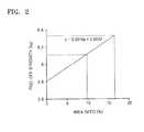
- FIG. 2 is a graph illustrating a peel-off strength (e.g., an adhesion strength) of the sealant 400 based on an area of the plurality of penetration holes ILH1 and ILH2 in the insulating layer IL of the organic light-emitting display apparatus of FIG. 1 .
- a peel-off strength e.g., an adhesion strength
- a unit of the peel-off strength is a weight (kg) applied on 19 mm width X 19 mm height area; a unit of the ratio is a percentage (%).
- a maximum peel-off strength that the organic light-emitting display apparatus may be able to endure in a general usage environment may be, for example, 6.11 kg.
- the maximum peel-off strength may be regarded as a maximum impact force that may be applied to the organic light-emitting display apparatus when the organic light-emitting display apparatus makes an impact with a surface (e.g., by falling or being dropped on a surface or the ground).
- the ratio of the area of the sealant 400 to the area of the plurality of penetration holes ILH1 and ILH2 in the insulating layer IL is to be about 9.8% or more, as shown using a dotted line in FIG. 2 .
- the organic light-emitting display apparatus may include a metal layer 150' (conductive layer) which is formed between the lower substrate 110 and the insulating layer IL in the peripheral area PA and includes a plurality of penetration openings 150A.
- the metal layer 150' may be extended into the display area DA.
- the metal layer 150' may include the same material as that of the gate electrode 150.
- the metal layer 150' and the gate electrode 150 may be formed on the same layer.
- the metal layer 150' is illustrated as being formed on the gate insulating film 140, like the gate electrode 150.
- the metal layer 150' may include the same material and be formed on the same layer as that of the source/drain electrode 170 of the thin film transistor TFT.
- the metal layer 150' includes the same material and is formed on the same layer as that of the gate electrode 150 will be described hereinafter.
- UV light or a laser beam may irradiate the sealant 400 to cure the sealant 400.
- the UV light or laser beam may penetrate through the upper substrate 300 and irradiate the sealant 400.
- the UV light or laser beam that has reached the sealant 400 may be reflected off the metal layer 150' under the sealant 400, and be redirected toward the sealant 400. Therefore, the UV light or laser beam may irradiate the sealant 400 more efficiently.
- An area of the sealant 400 contacting the upper substrate 300 may be relatively easily observed through the upper substrate 300 formed of a transparent material. However, the area of the sealant 400 contacting the lower substrate 110 may not be observed through the opaque metal layer 150'. Therefore, by including the plurality of penetration openings 150A in the metal layer 150', depending on whether or not the sealant 400 may be observed through the plurality of penetration openings 150A in the metal layer 150', the area of the sealant 400 contacting the lower substrate 110 may be identified. Accordingly, a faulty sealing may be easily identified by identifying whether or not the area of the sealant 400 contacting the upper substrate 300 and/or lower substrate 110 are/is the same as or greater than a minimum value of an area (e.g., a predetermined area).
- a minimum value of an area e.g., a predetermined area
- An inner surface 150a' of each of the plurality of penetration openings 150A in the metal layer 150' may be covered by using the insulating layer IL so as to not contact the sealant 400.
- the metal layer 150' is covered by using the interlayer insulating film 160, and accordingly, the inner surface 150a' of each of the plurality of penetration openings 150A in the metal layer 150' does not contact the sealant 400.
- the plurality of penetration holes ILH1 and ILH2 in the insulating layer IL may be formed by concurrently (e.g., simultaneously) etching the buffer layer 120, gate insulating film 140, and interlayer insulating film 160.
- the metal layer 150' in which the plurality of penetration openings 150A are already formed may be additionally etched.
- problems such as enlargement of an area of the plurality of penetration openings 150A in the metal layer 150' may occur.
- the inner surface 150a' of each of the plurality of penetration openings 150A in the metal layer 150' may be covered by using the insulating layer IL so as to not contact the sealant 400.
- a problem that may occur when the area of the plurality of penetration openings 150A in the metal layer 150' is larger than a predetermined area will be described below.
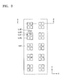
- FIG. 3 is a plan view illustrating the plurality of penetration holes in the insulating layer IL of an organic light-emitting display apparatus, according to another embodiment of the present invention.
- FIG. 1 may be interpreted as a cross-sectional view according to the line I-I of FIG. 3 .
- the sealant 400 is illustrated, and the plurality of penetration holes in the insulating layer IL that are formed under the sealant 400 are illustrated in solid lines for convenience.
- the insulating layer IL of the organic light-emitting display apparatus includes a plurality of penetration holes sets ILHS.
- Each of the plurality of penetration hole sets may include two or more penetration holes.
- An embodiment in which each of the plurality of penetration hole sets includes four penetration holes is illustrated in FIG. 3 .
- a distance ILHT between two or more penetration holes of each of the plurality of penetration hole sets ILHS in the insulating layer IL may be 2.5 ⁇ m or more.
- the distance ILHT is less than 2.5 ⁇ m, an area of the sealant 400 contacting the insulating layer IL may be reduced.
- the insulating layer IL between the adjacent penetration holes may collapse and form a single penetration hole.
- the distance ILHT is not a distance between the center of the plurality of penetration holes, but a distance between an inner surface of a penetration hole facing another penetration hole and an inner surface of another penetration hole facing a penetration hole, when a penetration hole and another penetration hole are adjacent to each other. That is, the distance ILHT may be regarded as a thickness of the insulating layer IL between the plurality of penetration holes.
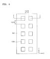
- FIG. 4 is a plan view illustrating a plurality of penetration openings 150A in the metal layer 150' of an organic light-emitting display apparatus, according to another embodiment of the present invention.
- FIG. 1 may be interpreted as a cross-sectional view according to the line I-I of FIG. 4 .
- the metal layer 150' may include the plurality of penetration openings 150A that are arranged repeatedly as shown in FIG. 4 . As described above, depending on whether or not the sealant 400 may be observed through the plurality of penetration openings 150A in the metal layer 150', the area of the sealant 400 contacting the lower substrate 110 may be identified.
- the plurality of penetration hole sets ILHS in the insulating layer IL may be formed to correspond to the plurality of penetration openings 150A in the metal layer 150'.
- the plurality of penetration holes included in the plurality of penetration hole sets ILHS may be extended to the buffer layer 120 through the plurality of penetration openings 150A in the metal layer 150', in which the buffer layer 120 is positioned directly above the lower substrate 110. Accordingly, because the sealant 400 may directly contact the lower substrate 110, an adhesion strength of the sealant 400 may be improved.
- each inner surface 150a' of the plurality of penetration openings 150A in the metal layer 150' may be covered by using the insulating layer IL so as to not contact the sealant 400.
- an area of each of the plurality of penetration hole sets ILHS in the insulating layer IL may be narrower than an area of each of the plurality of penetration openings 150A, as shown in FIGS. 3 and 4 .
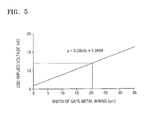
- FIG. 5 is a graph illustrating electrostatic discharge (ESD) durability according to a distance 150'W between the plurality of penetration openings 150A in the metal layer 150' (hereinafter, referred to as "distance 150'W") of the organic light-emitting display apparatus of FIG. 4 .
- the metal layer 150' may be formed on the same layer as that of the gate electrode 150 of the thin film transistor TFT in the display area DA.
- the distance 150'W may be regarded as a width of a gate metal wiring.
- the narrower the width of the gate metal wiring the larger the resistance of the gate metal wiring. Therefore, even when static electricity of equal strength is applied to the metal layer 150', the narrower the width of the gate metal wiring, the greater the amount of heat that may be generated momentarily. As the amount of heat generated in the metal layer 150' increases, the adhesive properties of the sealant may decrease (e.g., the sealant 400 may peel off) or a degree of hardness of the sealant 400 may be reduced. Thus, the width of the gate metal wiring, that is, the distance 150'W, is to be appropriately adjusted.
- the y-axis shows values of a strength of static electricity that may be applied to the metal layer 150', that is an ESD applied voltage;
- the x-axis shows a minimum width of the gate metal wiring that may cause the sealant 400 to peel off or a degree of hardness of the sealant 400 to be reduced, when the values of a strength of static electricity is applied to the metal layer 150'.
- a unit of the width of the gate metal wiring is ⁇ m; a unit of the ESD applied voltage is kV.
- static electricity may be generated during a process of manufacturing an organic light-emitting display apparatus or during a process of using the organic light-emitting display apparatus, and the static electricity may be transmitted to the metal layer 150'.
- resistance of the metal layer 150' is large, heat may be generated in the metal layer 150' and thus weaken an adhesion strength of the (cured) sealant 400 or reduce hardness of the sealant 400.
- a maximum ESD applied voltage that the organic light-emitting display apparatus may be able to endure in a general usage environment is 12kV.
- the maximum ESD applied voltage may be regarded as a maximum strength of static electricity that may be applied to an organic light-emitting display apparatus when manufacturing or using the organic light-emitting display apparatus in a general usage environment.
- the distance 150'W may be about 20.5 ⁇ m or more, as shown using a dotted line in FIG. 5 .
- the distance 150'W may be about 20.5 ⁇ m or more, in the surface parallel to the lower substrate 110 (the XY surface), the area of each of the plurality of penetration openings 150A in the metal layer 150' has an upper limit. Accordingly, the area of the plurality of penetration holes in the insulating layer IL, which are positioned in the plurality of penetration openings 150A in the metal layer 150', may also have an upper limit.
- the distance 150'W is about 20.5 ⁇ m, in the surface parallel to the lower substrate 110 (the XY surface), the area of the plurality of penetration holes in the insulating layer IL may be about 16.5% of or less than the area of the sealant 400.
- a ratio of the area of the plurality of penetration holes ILH1 and ILH2 in the insulating layer IL to the area of the sealant 400 may be between about 9.8% and about 16.5%.
- the insulating layer IL is illustrated as including the buffer layer 120, gate insulating film 140 and interlayer insulating film 160 in FIG. 1 , the insulating layer IL is not limited thereto.
- the first insulating film 181 may be extended to the peripheral area PA and thus be included in the insulating layer IL as an element thereof, and may include a plurality of penetration holes in the peripheral area PA.
- FIG. 6 is a cross-sectional view illustrating a portion of the organic light-emitting display apparatus according to another embodiment of the present invention.
- the insulating layer IL includes only the gate insulating film 140 and the interlayer insulating film 160, and the buffer layer 120 does not include a penetration hole.
- the buffer layer 120 may be regarded as a second insulating layer recited in the claim that is positioned between the lower substrate 110 and the insulating layer IL.
- the insulating layer IL may be regarded as an extended portion of at least one of the buffer layer 120, the gate insulating film 140, the interlayer insulating film 160, and the first insulating film 181 that is a protective film.
- FIG. 7 is a plan view illustrating a plurality of penetration openings 150A in a metal layer of the organic light-emitting display apparatus according to still another embodiment of the present invention.
- FIG. 1 may be interpreted as a cross-sectional view according to the line I-I of FIG. 7 .
- the organic light-emitting display apparatus may include the metal layer 150' which is formed between the lower substrate 110 and the insulating layer IL in the peripheral area PA or formed in the insulating layer IL in the peripheral area PA, includes a plurality of penetration openings 150A, and includes a width-change part.
- FIG 1 shows that the metal layer 150' is formed in the insulating layer IL, i.e., the metal layer 150' is interposed between the gate insulating film 120 and the interlayer insulating film 160.
- FIG 7 shows that the metal layer 150' includes the width-change part, the width of which decreases from W1 to W2 and then increases from W2 to W1 in +y-axis direction.
- the metal layer 150' may be extended into the display area DA.
- the metal layer 150' may shield an electromagnetic wave due to the characteristics of the metal.
- the metal layer 150' in the organic light-emitting display apparatus may shield the electromagnetic wave so that receiving sensibility of an antenna may decrease.
- the metal layer 150' includes the width-change part.
- the width-change part which is formed to correspond to the position of the antenna.
- a portion A shown in FIG. 7 may corresponds to the position of the antenna.
- the width-change part of the metal layer 150' may be formed in other positions which does not correspond to the position of the antenna. For example, if a certain part of the edge portion of the organic light-emitting display apparatus is vulnerable to static electricity, the width-change part of the metal layer 150' may correspond to the certain part. Because the static electricity may be induced by the metal layer 150', it is possible to decrease the possibility of the static electricity inducement by the width-change part wherein the width of the metal layer 150' decreases.
- the insulating layer IL may include a first portion and a second portion.
- the first portion of the insulating layer IL contacts a layer beneath the metal layer 150' through the plurality of penetration openings 150A of the metal layer 150', and the second portion of the insulating layer IL contacts the layer beneath the metal layer 150' outside the metal layer 150' in a portion of the width-change part in which the width of the metal layer 150' decreases.
- the first portion of the insulating layer IL contacts the lower substrate 110 through the plurality of penetration openings 150A of the metal layer 150', and the second portion of the insulating layer IL contacts the lower substrate 110 directly outside of the metal layer 150' in the portion A.
- FIG. 8 is a cross-sectional view illustrating a portion of the organic light-emitting display apparatus, according to still another embodiment of the present invention.
- the metal layer 150' may be formed between the lower substrate 110 and the insulating layer IL in the peripheral area PA or formed in the insulating layer IL in the peripheral area PA, includes a plurality of penetration openings 150A.
- the metal layer 150' is formed in the peripheral area PA, however, the metal layer 150' is formed to be located biasedly to the display area DA in relation with the center of the peripheral area PA. For example, the metal layer 150' is located biasedly to the display area DA in relation with the central axis 400CA of the sealant 400.
- the metal layer 150' is located biasedly to the display area DA in relation with the center of the peripheral area PA.
- the metal layer 150' does not exist in the most part of a outer region of the organic light-emitting display apparatus in relation with the central axis 400CA of the sealant 400. Therefore, the plurality of penetration holes ILH3 of the insulating layer IL may be formed regardless of the penetration openings 150A of the metal layer 150' in that region.
- the number of the penetration holes ILH3 of the insulating layer IL per unit area in a region where the insulating layer IL does not correspond to the metal layer 150' may be higher than the number of the penetration holes ILH1 and ILH2 of the insulating layer per unit area in a region where the insulating layer IL corresponds to the metal layer 150'.
- the metal layer 150' still exists in a region of the peripheral area PA in a direction to the display area DA. This is in order to protect the intermediate layer 220 of the plurality of OLEDs 200.
- the intermediate layer 220 is vulnerable to the impurities such as oxide or moisture. Thus, it is necessary to increase hardness of a portion of the sealant 400, the portion being close to the display area DA.
- the portion of the sealant 400 In order to increase hardness of the portion of the sealant 400, it is necessary to irradiate the portion of the sealant 400 with the UV light or the laser beam sufficiently. Because the metal layer 150' still exists in the region of the peripheral area PA in a direction to the display area DA, the UV light or the laser beam irradiated onto the sealant 400 and penetrating the sealant 400 is reflected by the metal layer 150' and reaches the sealant 400 again, thus the portion of the sealant 400 is sufficiently irradiated by the UV light or the laser beam.
- FIG. 9 is a cross-sectional view illustrating a portion of the organic light-emitting display apparatus, according to still another embodiment of the present invention.
- the organic light-emitting display apparatus comprises a dummy semiconductor layer 130'.
- the dummy semiconductor layer 130' may be formed on or under the insulating layer IL in the peripheral area PA, or formed in the insulating layer IL in the peripheral area PA.
- the dummy semiconductor layer 130' has a plurality of penetration apertures corresponding to the plurality of penetration holes ILH1 and ILH2.
- FIG. 9 shows that the dummy semiconductor layer 130' locates in the insulating layer IL, i.e., locates between the buffer layer 120 and the gate insulating layer 140.
- the sealant 400 fills the plurality of penetration holes ILH1 and ILH2 and the plurality of penetration apertures.
- the depth of the plurality of penetration holes ILH1 and ILH2 becomes deeper due to the presence of the dummy semiconductor layer 130'.
- This increase in depth means the increase of contact area between the sealant 400 and the insulating layer IL (including the dummy semiconductor layer 130'), thus the adhesion strength between the sealant 400 and the lower substrate 110 becomes strong.
- the dummy semiconductor layer 130' may include the same material as that of the semiconductor layer 130. Specifically, the dummy semiconductor layer 130' and the semiconductor layer 130 may be formed on the same layer. In FIG. 9 , the dummy semiconductor layer 130' is illustrated as being formed on the buffer layer 120, like the semiconductor layer 130.
- an organic light-emitting display apparatus is described above, the present invention is not limited thereto.
- a method of manufacturing an organic light-emitting display apparatus may also be included in the scope of the present invention.
- the method includes preparing the lower substrate 110 which includes the display area DA and the peripheral area PA that surrounds the display area DA; and forming the insulating layer IL over the display area DA and the peripheral area DA of the lower substrate 110, and includes forming the plurality of penetration holes ILH1 and ILH2 in the peripheral area PA.
- the buffer layer 120, gate insulating film 140 and interlayer insulating film 160 may be formed over the display area DA and the peripheral area PA of the lower substrate 110. Then, a penetration hole that exposes a portion of the source/drain electrodes 170 of the thin film transistor TFT in the display area DA may be formed to couple the pixel electrode 210 to the source/drain electrodes 170. At the same time, the plurality of penetration holes ILH1 and ILH2 penetrating through the buffer layer 120, gate insulating film 140 and interlayer insulating film 160 in the peripheral area PA may be formed.
- the insulating layer IL may be regarded as including the buffer layer 120, gate insulating film 140 and interlayer insulating film 160.
- the insulating film IL may include at least one of the buffer layer 120, gate insulating film 140, and interlayer insulating layer 160 (in FIG. 6 , the insulating layer IL may be regarded as not including the gate insulating film 140 and interlayer insulating film 160), and/or further include at least one of the first protective film 181 and second protective film 182.
- the OLED 200 and other elements are formed.
- the upper substrate 300 which corresponds to the lower substrate 100 is prepared.
- the upper substrate 300 may be prepared before processing the lower substrate 110, or the upper substrate 300 may be prepared while processing the lower substrate 110.
- processing the lower substrate 110 may mean forming the insulating layer IL on the lower substrate 110, etc..
- the plurality of penetration holes in the insulating layer IL are filled (or substantially filled) with the sealant 400, and the lower and upper substrates 110 and 300 are bonded to each other by using the sealant 400.
- the metal layer 150' which is located in the peripheral area PA of the lower substrate 110 and includes the plurality of penetration openings 150A may be formed.
- the metal layer 150' may be formed to be positioned between the lower substrate 110 and the insulating layer IL.
- the insulating layer IL may be formed to include the plurality of penetration hole sets ILHS that correspond to the plurality of penetration openings 150A in the metal layer 150', in which each of the plurality of penetration hole sets ILHS includes two or more penetration holes.
- the insulating layer IL may be formed so that a minimum distance between two or more penetration holes in each of the plurality of penetration hole sets ILHS in the insulating layer 150 is about 2.5 ⁇ m or more.
- the minimum distance may provide the same characteristics as described earlier above.
- the metal layer 150' may be formed so that a minimum distance between the plurality of penetration openings 150A is about 20.5 ⁇ m or more.
- the minimum distance may provide the same characteristics as described earlier above with respect to static electricity.
- the insulating layer IL may be formed so that in the surface parallel to the lower substrate 110 (the XY surface), a total area of the plurality of penetration holes ILH1 and ILH2 in the insulating layer IL may be between about 9.8% and about 16.5% of the area of the sealant 400.
- the lower limit and upper limit may provide the same characteristics as described earlier above.
- the buffer layer 120, gate insulating film 140, and interlayer insulating film 160 may be formed over the display area DA and the peripheral area PA of the lower substrate 110; and the plurality of penetration holes penetrating through the buffer layer 120, gate insulating film 140, and interlayer insulating film 160 may be formed.
- the metal layer 150' may be formed to have a width-change part in which the width of the metal layer 150' changes, as shown in FIG. 7 .
- the metal layer 150' may be formed biasedly to the display area DA, as shown in FIG. 8 .
- a dummy semiconductor layer 130' may be formed on or under the insulating layer IL in the peripheral area PA, or formed in the insulating layer IL in the peripheral area PA, as shown in FIG. 9 .
- the dummy semiconductor layer 130' may have a plurality of penetration apertures corresponding to the plurality of penetration holes ILH1 and ILH2.
- the dummy semiconductor layer 130' may be formed to include the same material as that of the semiconductor layer 130. Specifically, the dummy semiconductor layer 130' and the semiconductor layer 130 may be formed on the same layer.
- an organic light-emitting display apparatus in which shock damage may be reduced and a method of manufacturing the same are provided.
Landscapes
- Engineering & Computer Science (AREA)
- Microelectronics & Electronic Packaging (AREA)
- Physics & Mathematics (AREA)
- Optics & Photonics (AREA)
- Electroluminescent Light Sources (AREA)
- Devices For Indicating Variable Information By Combining Individual Elements (AREA)
Abstract
Description
- One or more embodiments of the present invention relate to an organic light-emitting display apparatus and a method of manufacturing the same.
- In general, an organic light-emitting display apparatus is manufactured by forming organic light-emitting diodes (OLEDs) on a lower substrate, and bonding the lower substrate and an upper substrate such that the OLEDs are positioned between the lower and upper substrates. The organic light-emitting display apparatus may be used as a display unit in small devices such as cellular phones, and in large devices such as televisions.
- In the organic light-emitting display apparatus, a sealant is used to bond the lower and upper substrates. A region in which the sealant is disposed is regarded as a dead space, which is a non-display region.
- One or more embodiments of the present invention include an organic light-emitting display apparatus in which shock damage may be reduced and a method of manufacturing the same.
- Additional aspects will be set forth in part in the description which follows and, in part, will be apparent from the description, or may be learned by practice of the presented embodiments.
- According to one or more embodiments of the present invention, an organic light-emitting display apparatus includes a lower substrate comprising a display area and a peripheral area around the display area; a first insulating layer on the display area and the peripheral area of the lower substrate, wherein a plurality of penetration holes are formed in the first insulating layer in the peripheral area; an upper substrate on the lower substrate; and a sealant in the plurality of penetration holes bonding the lower substrate to the upper substrate.
- The organic light-emitting display apparatus may further include a second insulating layer between the upper substrate and the first insulating layer.
- The organic light-emitting display apparatus may further include a conductive layer between the lower substrate and first the insulating layer, wherein a plurality of penetration openings are formed in the conductive layer.
- The first insulating layer may include a plurality of penetration hole sets that correspond to the plurality of penetration openings in the conductive layer, and each of the plurality of penetration hole sets may include two or more of the penetration holes.
- An area of each of the plurality of penetration hole sets in the first insulating layer may be narrower than an area of each of the plurality of penetration openings in the conductive layer.
- An inner surface of each of the plurality of penetration openings in the conductive layer may be covered by the first insulating layer, and may not contact the sealant.
- A distance between the two or more of the penetration holes in each of the plurality of penetration hole sets in the first insulating layer may be 2.5 µm or more.
- An inner surface of each of the plurality of penetration openings in the conductive layer may be covered by the first insulating layer, and may not contact the sealant.
- A distance between the plurality of penetration openings in the conductive layer may be 20.5 µm or more.
- The display area may include a thin film transistor including a gate electrode, and the conductive layer may include a same material as that of the gate electrode in the thin film transistor.
- The conductive layer and the gate electrode may be disposed on a same layer.
- In a surface parallel to the lower substrate, a total area of the plurality of penetration holes in the first insulating layer may be in a range of 9.8% and 16.5% of an area of the sealant.
- The display area may include a buffer layer, a gate insulating film, an interlayer insulating film, and a protective film, and the first insulating layer may be an extended portion of at least one of the buffer layer, the gate insulating film, the interlayer insulating film, and the protective film.
- The organic light-emitting display apparatus may further comprise a conductive layer interposed between the lower substrate and the first insulating layer or located in the first insulating layer, wherein the conductive layer locates in the peripheral area, has a plurality of penetration openings, and has a width-change part in which a width of the conductive layer changes.
- The first insulating layer may have a first portion and a second portion, the first portion contacting a layer beneath the conductive layer through the plurality of penetration openings of the conductive layer, the second portion contacting the layer beneath the conductive layer outside the conductive layer in a region of the width-change part of the conductive layer.
- The organic light-emitting display apparatus may further comprise a conductive layer interposed between the lower substrate and the insulating layer or located in the first insulating layer, wherein the conductive layer locates in the peripheral area and locates biasedly to the display area.
- The number of the plurality of penetration holes of the first insulating layer per unit area in a region where the first insulating layer does not correspond to the conductive layer may be higher than the number of the plurality of penetration holes of the first insulating layer per unit area in a region where the first insulating layer corresponds to the conductive layer.
- The organic light-emitting display apparatus may further comprises a dummy semiconductor layer on or under the first insulating layer or in the first insulating layer, wherein the dummy semiconductor layer locates in the peripheral area, and has a plurality of penetration apertures corresponding to the plurality of penetration holes of the first insulating layer, and wherein the sealant fills the plurality of penetration apertures and the plurality of penetration holes.
- The display area may comprise a thin film transistor comprising a semiconductor layer, and the dummy semiconductor layer may comprise a same material as that of the semiconductor layer in the thin film transistor.
- The dummy semiconductor layer and the semiconductor layer may be disposed on a same layer.
- According to another embodiment of the present invention, a method of manufacturing an organic light-emitting display apparatus includes: preparing a lower substrate comprising a display area and a peripheral area around the display area; forming an insulating layer over the display area and the peripheral area of the lower substrate; forming a plurality of penetration holes in the peripheral area; arranging an upper substrate to corresponds to the lower substrate; and bonding the lower substrate and the upper substrate by using a sealant, the sealant filling the plurality of penetration holes in the insulating layer.
- The method may further include forming a conductive layer in the peripheral area of the lower substrate, the conductive layer comprising a plurality of penetration openings, and wherein forming the insulating layer comprises forming the insulating layer so that the conductive layer is between the lower substrate and the insulating layer.
- The method may further include forming a plurality of penetration hole sets in the insulating layer that correspond to the plurality of penetration openings in the conductive layer, wherein each of the plurality of penetration hole sets comprise two or more of the penetration holes.
- A distance between the two or more of the penetration holes in each of the plurality of penetration hole sets in the insulating layer may be 2.5 µm or more.
- A distance between the plurality of penetration openings may be 20.5 µm or more.
- A total area of the plurality of penetration holes in the insulating layer may be in a range of 9.8% and 16.5% of an area of the sealant.
- Forming the insulating layer may include forming a buffer layer, a gate insulating film, an interlayer insulating film, and a protective film over the display area and the peripheral area of the lower substrate, and forming the plurality of penetration holes through the buffer layer, the gate insulating film, the interlayer insulating film, and the protective film.
- At least some of the above and other features of the invention are set out in the claims.
- Aspects of the present invention will become more apparent and more readily appreciated from the following description of the embodiments, taken in conjunction with the accompanying drawings of which:
-
FIG. 1 is a cross-sectional view illustrating a portion of an organic light-emitting display apparatus, according to an embodiment of the present invention; -
FIG. 2 is a graph illustrating a peel-off strength of a sealant according to an area of a plurality of penetration holes in an insulating layer of the organic light-emitting display apparatus ofFIG. 1 ; -
FIG. 3 is a plan view illustrating the plurality of penetration holes in the insulating layer of an organic light-emitting display apparatus, according to another embodiment of the present invention; -
FIG. 4 is a plan view illustrating a plurality of penetration openings in a metal layer of an organic light-emitting display apparatus, according to another embodiment of the present invention; -
FIG. 5 is a graph illustrating electrostatic discharge (ESD) durability according to a distance between the plurality of penetration openings in the metal layer of the organic light-emitting display apparatus ofFIG. 4 ; -
FIG. 6 is a cross-sectional view illustrating a portion of the organic light-emitting display apparatus, according to another embodiment of the present invention; -
FIG. 7 is a plan view illustrating a plurality of penetration openings in a metal layer of the organic light-emitting display apparatus, according to still another embodiment of the present invention; -
FIG. 8 is a cross-sectional view illustrating a portion of the organic light-emitting display apparatus, according to still another embodiment of the present invention; and -
FIG. 9 is a cross-sectional view illustrating a portion of the organic light-emitting display apparatus, according to still another embodiment of the present invention. - Reference will now be made in some detail to embodiments, examples of which are illustrated in the accompanying drawings, wherein like reference numerals refer to the like elements throughout. In this regard, the present embodiments may have different forms and should not be construed as being limited to the descriptions set forth herein. Accordingly, the embodiments are merely described below, by referring to the figures, to explain aspects of the present invention. Also, the thickness or size of each layer illustrated in the drawings is exaggerated for convenience of explanation and clarity.
- In the following description, an x-axis, a y-axis, and a z-axis are not limited to three axes on a rectangular coordinate system and may be interpreted in a broader sense. For example, the x-axis, y-axis, and z-axis may be perpendicular to one another or may indicate different directions that are not perpendicular to one another.
- Also, in the following description, when a constituent element such as a layer, a film, a region, or a plate is described to exist on another constituent element, the constituent element may exist directly on the other constituent element or another constituent element may be disposed therebetween.
- As used herein, the term "and/or" includes any and all combinations of one or more of the associated listed items. Expressions such as "at least one of," when preceding a list of elements, modify the entire list of elements and do not modify the individual elements of the list.
-
FIG. 1 is a cross-sectional view illustrating a portion of an organic light-emitting display apparatus, according to an embodiment of the present invention. Referring toFIG. 1 , the organic light-emitting display apparatus according to an embodiment of the present invention includes alower substrate 110, anupper substrate 300, an insulating layer IL, and asealant 400. - The
lower substrate 110 includes a display area DA and a peripheral area PA that surrounds the display area DA. Thelower substrate 110 may be formed by using various materials such as glass, metal, or plastic. A plurality of thin film transistors TFT are positioned in the display area DA of thelower substrate 110. Also, a plurality of organic light-emitting diodes (OLEDs) 200 that are electrically coupled to the plurality of thin film transistors TFT may be positioned in the display area DA. When theOLEDs 200 are electrically coupled to the plurality of the thin film transistors TFT, such a connection may be regarded as a plurality ofpixel electrodes 210 being electrically coupled to the plurality of thin film transistors TFT. - Each thin film transistor TFT includes a
semiconductor layer 130 that includes amorphous silicon or poly silicon, or an organic semiconductor; agate electrode 150; and source/drain electrodes 170. On thelower substrate 110, abuffer layer 120 formed of silicon oxide or silicon nitride is positioned, so as to planarize a surface of thelower substrate 110 or to prevent impurities from penetrating into thesemiconductor layer 130. Thesemiconductor layer 130 may be positioned on thebuffer layer 120. - The
gate electrode 150 is positioned on thesemiconductor layer 130. The source/drain electrodes 170 electrically communicate with each other according to a signal that is applied to thegate electrode 150. Depending on an adhesion strength between adjacent layers, a degree of surface planarization of stacked layers, and processability, thegate electrode 150 may be formed to have a single or multi-layer structure by using at least one of materials such as aluminum (Al), platinum (Pt), palladium (Pd), silver (Ag), magnesium (Mg), gold (Au), nickel (Ni), neodymium (Nd), iridium (Ir), chromium (Cr), lithium (Li), calcium (Ca), molybdenum (Mo), titanium (Ti), tungsten (W), and copper (Cu). Agate insulating film 140, which is formed by using a material such as silicon oxide and/or silicon nitride, may be formed between thesemiconductor layer 130 and thegate electrode 150 to insulate thesemiconductor layer 130 from thegate electrode 150. - An interlayer insulating
film 160 may be positioned on thegate electrode 150, and may be formed to have a single or multi-layer structure by using materials such as silicon oxide or silicon nitride. - The source/
drain electrodes 170 are positioned on theinterlayer insulating film 160. The source/drain electrodes 170 are electrically coupled to thesemiconductor layer 130 respectively through contact holes, which are formed in theinterlayer insulating film 160 and thegate insulating film 140. In consideration of conductivity, the source/drain electrodes 170 may be formed to have a single or multi-layer structure by using at least one of materials such as Al, Pt, Pd, Ag, Mg, Au, Ni, Nd, Ir, Cr, Li, Ca, Mo, Ti, W, and Cu. - A first insulating
film 181, which is a protective film covering the thin film transistor TFT to protect the thin film transistor TFT having a structure as described above, may be provided. The firstinsulating film 181 may be formed of inorganic materials such as silicon oxide, silicon nitride, or silicon oxynitride. Although the first insulatingfilm 181 is illustrated as a single layer inFIG. 1 , the first insulatingfilm 181 may be modified to have a multi-layer structure or may be modified in other various ways. - A second
insulating film 182 may be positioned on the first insulatingfilm 181. For example, when theOLED 200 is positioned on the thin film transistor TFT as shown inFIG. 1 , the secondinsulating film 182, which operates as a planarization film for planarizing an upper surface of the first insulatingfilm 181 that covers the thin film transistor TFT, may be provided. The secondinsulating film 182 may be formed of materials such as an acryl-based organic material or benzocyclobutene (BCB). Although the secondinsulating film 182 is illustrated as a single layer inFIG. 1 , the secondinsulating film 182 may be modified to have a multi-layer structure or may be modified in other various ways. - In the display area DA of the
lower substrate 110, theOLED 200, which includes thepixel electrode 210, anopposite electrode 230, and anintermediate layer 220 positioned between thepixel electrode 210 and theopposite electrode 230, is positioned on the secondinsulating film 182. - An opening, which exposes at least one of the source/
drain electrodes 170, is provided in the first and second insulatingfilms pixel electrode 210, which contacts either one of the source/drain electrodes 170 through the opening and thus is electrically coupled to the thin film transistor TFT, is positioned on the secondinsulating film 182. Thepixel electrode 210 may be a (semi) transparent electrode or a reflective electrode. When thepixel electrode 210 is a (semi) transparent electrode, thepixel electrode 210 may be formed of materials such as indium tin oxide (ITO), indium zinc oxide (IZO), zinc oxide (ZnO), indium oxide (In2O3), indium gallium oxide (IGO), or aluminum zinc oxide (AZO). When thepixel electrode 210 is a reflective electrode, thepixel electrode 210 may include a reflective film formed of Ag, Mg, Al, Pt, Pd, Au, Ni, Nd, Ir, Cr, or a compound thereof, and a layer formed of ITO, IZO, ZnO, In2O3, or AZO. A structure and a material of thepixel electrode 210 are not limited thereto, and may be modified in various ways. For example, thepixel electrode 210 may be formed to have a single or multi-layer structure. - A third
insulating film 183 may be positioned on the secondinsulating film 182. The thirdinsulating film 183 is a pixel defining film, which defines a pixel by having an opening corresponding to each sub-pixel, that is, an opening through which at least a central portion of thepixel electrode 210 is exposed. In addition, the thirdinsulating film 183 may prevent an arc or the like from occurring at an end portion of thepixel electrode 210 by increasing a distance between the end portion of thepixel electrode 210 and theopposite electrode 230 that is positioned on thepixel electrode 210. The thirdinsulating film 183 may be formed of an organic material such as polyimide. - The
intermediate layer 220 may include a low molecular weight material or a high molecular weight material. When theintermediate layer 220 includes a low molecular weight material, a hole injection layer (HIL), a hole transport layer (HTL), an emission layer (EML), an electron transport layer (ETL), or an electron injection layer (EIL) may be stacked to form a single or multiple layer structure. Also, various organic materials such as copper phthalocyanine (CuPc), N,N'-Di(naphthalene-1-yl)-N,N'-diphenyl-benzidine (NPB), or tris-8-hydroxyquinoline aluminum (Alq3) may be used to form theintermediate layer 220. Theintermediate layer 220 may be formed by any suitable method such as using a vacuum deposition method. - When the
intermediate layer 220 includes a high molecular weight material, theintermediate layer 220 may include the HTL and EML. In this case, the HTL may be formed of poly(3,4-ethylenedioxythiophene) (PEDOT), and the EML may be formed of a high molecular weight material such as poly-phenylenevinylene (PPV) or polyfluorene. Theintermediate layer 220 may be formed by using a method such as a screen printing method, an inkjet printing method, or a laser induced thermal imaging (LITI) method. - The
intermediate layer 220 is not limited to the structure described above, and may be modified in various ways. - The
opposite electrode 230 is positioned on the display area DA to cover the display area DA as shown inFIG. 1 . That is, theopposite electrode 230 may be integrally formed with a plurality ofOLEDs 200 and correspond to the plurality ofpixel electrodes 210. Theopposite electrode 230 may be a (semi) transparent electrode or a reflective electrode. When theopposite electrode 230 is a (semi) transparent electrode, theopposite electrode 230 may include a layer formed of a conductive material or metal having a low work function, that is, Li, Ca, LiF/Ca, LiF/Al, Al, Ag, Mg, or a compound thereof, and a (semi) transparent conductive layer formed of ITO, IZO, ZnO, or In2O3. A structure and a material of theopposite electrode 230 are not limited thereto, and may be modified in various ways. - The
upper substrate 300 corresponds to thelower substrate 110, and may be formed of various materials such as glass, metal, or plastic. The lower andupper substrates sealant 400. - The
buffer layer 120, thegate insulating film 140, and theinterlayer insulating film 160 may be referred collectively as the insulating layer IL (a first insulating layer recited in the claims). The insulating layer IL may be formed over the display area DA and the peripheral area PA of thelower substrate 110 as shown inFIG. 1 . The insulating layer IL includes a plurality of penetration holes ILH1 and ILH2 in the peripheral area PA. Thesealant 400 fills the plurality of penetration holes ILH1 and ILH2 of the insulating layer IL, and bonds thelower substrate 110 and theupper substrate 300. Thesealant 400 may include frit or epoxy, but is not limited thereto. - The insulating layer IL recited in the claims need not be construed as a stack structure including the
buffer layer 120, thegate insulating film 140, and theinterlayer insulating film 160. For example, the insulating layer IL recited in the claims may be construed as a stack structure including only theinterlayer insulating film 160. In this case, thebuffer layer 120 andgate insulating film 140 need not include the plurality of penetration holes ILH1 and ILH2. - For some cases, the insulating layer IL recited in the claims may include the
gate insulating film 140 and theinterlayer insulating film 160, thus thegate insulating film 140 and theinterlayer insulating film 160 may include the plurality of penetration holes ILH1 and ILH2, and thebuffer layer 120 need not be patterned. In these cases, thebuffer layer 120 may be regarded as a second insulating layer recited in the claim that is interposed between thelower substrate 110 and the insulating layer IL. - To use the
sealant 400 and relatively securely bond the lower andupper substrates width 400A of thesealant 400 inFIG. 1 ), the greater the dead space, that is, an area of the peripheral area PA, outside of the display area DA. Therefore, the area of thesealant 400 is to be decreased so as to reduce the dead space. In the organic light-emitting display apparatus according to an embodiment of the present invention, the insulating layer IL includes the plurality of penetration holes ILH1 and ILH2. Accordingly, while an area of thesealant 400 on a surface parallel to the lower substrate 110 (an XY surface) is reduced, an area of thesealant 400 that contacts elements on thelower substrate 110, that is, the insulating layer IL, may be maintained or expanded. Thus, by reducing the area of thesealant 400, the dead space may be reduced while an adhesion strength of thesealant 400 that bonds the lower andupper substrates -
FIG. 2 is a graph illustrating a peel-off strength (e.g., an adhesion strength) of thesealant 400 based on an area of the plurality of penetration holes ILH1 and ILH2 in the insulating layer IL of the organic light-emitting display apparatus ofFIG. 1 . In the surface parallel to the lower substrate 110 (the XY surface), a ratio of the area of thesealant 400 to the total area of the plurality of penetration holes ILH1 and ILH2 in the insulating layer IL is shown on an x-axis; and the peel-off strength, which is a force that separates thelower substrate 110 from thesealant 400, is shown on a y-axis. A relationship between the ratio of the area of thesealant 400 to the total area of the plurality of penetration holes ILH1 and ILH2 and the peel-off strength may be represented as y=0.0316x+5.8042, which is determined by carrying out an experiment multiple times. A unit of the peel-off strength is a weight (kg) applied on 19 mm width X 19 mm height area; a unit of the ratio is a percentage (%). - In mobile devices that include an organic light-emitting display apparatus as a display unit, a maximum peel-off strength that the organic light-emitting display apparatus may be able to endure in a general usage environment may be, for example, 6.11 kg. The maximum peel-off strength may be regarded as a maximum impact force that may be applied to the organic light-emitting display apparatus when the organic light-emitting display apparatus makes an impact with a surface (e.g., by falling or being dropped on a surface or the ground). In order to prevent the
sealant 400 from being faulty under such conditions, the ratio of the area of thesealant 400 to the area of the plurality of penetration holes ILH1 and ILH2 in the insulating layer IL is to be about 9.8% or more, as shown using a dotted line inFIG. 2 . - Referring back to
FIG. 1 , the organic light-emitting display apparatus may include ametal layer 150' (conductive layer) which is formed between thelower substrate 110 and the insulating layer IL in the peripheral area PA and includes a plurality ofpenetration openings 150A. Themetal layer 150' may be extended into the display area DA. As described above, because the display area DA includes the thin film transistor TFT including thegate electrode 150, themetal layer 150' may include the same material as that of thegate electrode 150. Specifically, themetal layer 150' and thegate electrode 150 may be formed on the same layer. InFIG. 1 , themetal layer 150' is illustrated as being formed on thegate insulating film 140, like thegate electrode 150. In some embodiments, themetal layer 150' may include the same material and be formed on the same layer as that of the source/drain electrode 170 of the thin film transistor TFT. For convenience of description, an embodiment in which themetal layer 150' includes the same material and is formed on the same layer as that of thegate electrode 150 will be described hereinafter. - When bonding the lower and
upper substrates sealant 400, ultraviolet (UV) light or a laser beam may irradiate thesealant 400 to cure thesealant 400. Specifically, the UV light or laser beam may penetrate through theupper substrate 300 and irradiate thesealant 400. Then, the UV light or laser beam that has reached thesealant 400 may be reflected off themetal layer 150' under thesealant 400, and be redirected toward thesealant 400. Therefore, the UV light or laser beam may irradiate thesealant 400 more efficiently. - An area of the
sealant 400 contacting theupper substrate 300 may be relatively easily observed through theupper substrate 300 formed of a transparent material. However, the area of thesealant 400 contacting thelower substrate 110 may not be observed through theopaque metal layer 150'. Therefore, by including the plurality ofpenetration openings 150A in themetal layer 150', depending on whether or not thesealant 400 may be observed through the plurality ofpenetration openings 150A in themetal layer 150', the area of thesealant 400 contacting thelower substrate 110 may be identified. Accordingly, a faulty sealing may be easily identified by identifying whether or not the area of thesealant 400 contacting theupper substrate 300 and/orlower substrate 110 are/is the same as or greater than a minimum value of an area (e.g., a predetermined area). - An
inner surface 150a' of each of the plurality ofpenetration openings 150A in themetal layer 150' may be covered by using the insulating layer IL so as to not contact thesealant 400. InFIG. 1 , themetal layer 150' is covered by using theinterlayer insulating film 160, and accordingly, theinner surface 150a' of each of the plurality ofpenetration openings 150A in themetal layer 150' does not contact thesealant 400. - The plurality of penetration holes ILH1 and ILH2 in the insulating layer IL may be formed by concurrently (e.g., simultaneously) etching the
buffer layer 120,gate insulating film 140, andinterlayer insulating film 160. During this process, when theinner surface 150a' of each of the plurality ofpenetration openings 150A in themetal layer 150' is exposed through the plurality of penetration holes ILH1 and ILH2, themetal layer 150' in which the plurality ofpenetration openings 150A are already formed may be additionally etched. Thus, problems such as enlargement of an area of the plurality ofpenetration openings 150A in themetal layer 150' may occur. To prevent or reduce such a problem from occurring, theinner surface 150a' of each of the plurality ofpenetration openings 150A in themetal layer 150' may be covered by using the insulating layer IL so as to not contact thesealant 400. A problem that may occur when the area of the plurality ofpenetration openings 150A in themetal layer 150' is larger than a predetermined area will be described below. -
FIG. 3 is a plan view illustrating the plurality of penetration holes in the insulating layer IL of an organic light-emitting display apparatus, according to another embodiment of the present invention.FIG. 1 may be interpreted as a cross-sectional view according to the line I-I ofFIG. 3 . - In
FIG. 3 , thesealant 400 is illustrated, and the plurality of penetration holes in the insulating layer IL that are formed under thesealant 400 are illustrated in solid lines for convenience. - As shown in
FIG. 3 , the insulating layer IL of the organic light-emitting display apparatus according to the present embodiment includes a plurality of penetration holes sets ILHS. Each of the plurality of penetration hole sets may include two or more penetration holes. An embodiment in which each of the plurality of penetration hole sets includes four penetration holes is illustrated inFIG. 3 . - A distance ILHT between two or more penetration holes of each of the plurality of penetration hole sets ILHS in the insulating layer IL (hereinafter, referred to as "distance ILHT") may be 2.5 µm or more. When the distance ILHT is less than 2.5 µm, an area of the
sealant 400 contacting the insulating layer IL may be reduced. Thus, the insulating layer IL between the adjacent penetration holes may collapse and form a single penetration hole. In this case, the distance ILHT is not a distance between the center of the plurality of penetration holes, but a distance between an inner surface of a penetration hole facing another penetration hole and an inner surface of another penetration hole facing a penetration hole, when a penetration hole and another penetration hole are adjacent to each other. That is, the distance ILHT may be regarded as a thickness of the insulating layer IL between the plurality of penetration holes. -
FIG. 4 is a plan view illustrating a plurality ofpenetration openings 150A in themetal layer 150' of an organic light-emitting display apparatus, according to another embodiment of the present invention.FIG. 1 may be interpreted as a cross-sectional view according to the line I-I ofFIG. 4 . Themetal layer 150' may include the plurality ofpenetration openings 150A that are arranged repeatedly as shown inFIG. 4 . As described above, depending on whether or not thesealant 400 may be observed through the plurality ofpenetration openings 150A in themetal layer 150', the area of thesealant 400 contacting thelower substrate 110 may be identified. - The plurality of penetration hole sets ILHS in the insulating layer IL may be formed to correspond to the plurality of
penetration openings 150A in themetal layer 150'. The plurality of penetration holes included in the plurality of penetration hole sets ILHS may be extended to thebuffer layer 120 through the plurality ofpenetration openings 150A in themetal layer 150', in which thebuffer layer 120 is positioned directly above thelower substrate 110. Accordingly, because thesealant 400 may directly contact thelower substrate 110, an adhesion strength of thesealant 400 may be improved. - As described above, each
inner surface 150a' of the plurality ofpenetration openings 150A in themetal layer 150' may be covered by using the insulating layer IL so as to not contact thesealant 400. To do so, an area of each of the plurality of penetration hole sets ILHS in the insulating layer IL may be narrower than an area of each of the plurality ofpenetration openings 150A, as shown inFIGS. 3 and4 . -
FIG. 5 is a graph illustrating electrostatic discharge (ESD) durability according to a distance 150'W between the plurality ofpenetration openings 150A in themetal layer 150' (hereinafter, referred to as "distance 150'W") of the organic light-emitting display apparatus ofFIG. 4 . As described above, themetal layer 150' may be formed on the same layer as that of thegate electrode 150 of the thin film transistor TFT in the display area DA. Thus, in the surface parallel to the lower substrate 110 (the XY surface), the distance 150'W may be regarded as a width of a gate metal wiring. - The narrower the width of the gate metal wiring, the larger the resistance of the gate metal wiring. Therefore, even when static electricity of equal strength is applied to the
metal layer 150', the narrower the width of the gate metal wiring, the greater the amount of heat that may be generated momentarily. As the amount of heat generated in themetal layer 150' increases, the adhesive properties of the sealant may decrease (e.g., thesealant 400 may peel off) or a degree of hardness of thesealant 400 may be reduced. Thus, the width of the gate metal wiring, that is, the distance 150'W, is to be appropriately adjusted. - In
FIG. 5 , the y-axis shows values of a strength of static electricity that may be applied to themetal layer 150', that is an ESD applied voltage; the x-axis shows a minimum width of the gate metal wiring that may cause thesealant 400 to peel off or a degree of hardness of thesealant 400 to be reduced, when the values of a strength of static electricity is applied to themetal layer 150'. A relationship between the minimum width of the gate metal wiring and the strength of the ESD applied voltage may be represented, for example, as y=0.2959x+5.9694, which is determined by carrying out an experiment multiple times. A unit of the width of the gate metal wiring is µm; a unit of the ESD applied voltage is kV. - As described above, static electricity may be generated during a process of manufacturing an organic light-emitting display apparatus or during a process of using the organic light-emitting display apparatus, and the static electricity may be transmitted to the
metal layer 150'. In this case, when resistance of themetal layer 150' is large, heat may be generated in themetal layer 150' and thus weaken an adhesion strength of the (cured)sealant 400 or reduce hardness of thesealant 400. - In mobile devices that include an organic light-emitting display apparatus as a display unit, a maximum ESD applied voltage that the organic light-emitting display apparatus may be able to endure in a general usage environment is 12kV. The maximum ESD applied voltage may be regarded as a maximum strength of static electricity that may be applied to an organic light-emitting display apparatus when manufacturing or using the organic light-emitting display apparatus in a general usage environment. In order to prevent the
sealant 400 from being faulty in such an environment, in a surface parallel to the lower substrate 110 (XY surface), the distance 150'W may be about 20.5 µm or more, as shown using a dotted line inFIG. 5 . - Because the distance 150'W may be about 20.5 µm or more, in the surface parallel to the lower substrate 110 (the XY surface), the area of each of the plurality of
penetration openings 150A in themetal layer 150' has an upper limit. Accordingly, the area of the plurality of penetration holes in the insulating layer IL, which are positioned in the plurality ofpenetration openings 150A in themetal layer 150', may also have an upper limit. When the distance 150'W is about 20.5 µm, in the surface parallel to the lower substrate 110 (the XY surface), the area of the plurality of penetration holes in the insulating layer IL may be about 16.5% of or less than the area of thesealant 400. Thus, in the surface parallel to the lower substrate 110 (the XY surface), a ratio of the area of the plurality of penetration holes ILH1 and ILH2 in the insulating layer IL to the area of thesealant 400 may be between about 9.8% and about 16.5%. - Although the insulating layer IL is illustrated as including the
buffer layer 120,gate insulating film 140 and interlayer insulatingfilm 160 inFIG. 1 , the insulating layer IL is not limited thereto. For example, the first insulatingfilm 181 may be extended to the peripheral area PA and thus be included in the insulating layer IL as an element thereof, and may include a plurality of penetration holes in the peripheral area PA. -
FIG. 6 is a cross-sectional view illustrating a portion of the organic light-emitting display apparatus according to another embodiment of the present invention. Referring toFIG. 6 , the insulating layer IL includes only thegate insulating film 140 and theinterlayer insulating film 160, and thebuffer layer 120 does not include a penetration hole. In this case, thebuffer layer 120 may be regarded as a second insulating layer recited in the claim that is positioned between thelower substrate 110 and the insulating layer IL. - Accordingly, the insulating layer IL may be regarded as an extended portion of at least one of the
buffer layer 120, thegate insulating film 140, theinterlayer insulating film 160, and the first insulatingfilm 181 that is a protective film. -
FIG. 7 is a plan view illustrating a plurality ofpenetration openings 150A in a metal layer of the organic light-emitting display apparatus according to still another embodiment of the present invention. In this case,FIG. 1 may be interpreted as a cross-sectional view according to the line I-I ofFIG. 7 . - Referring to
FIGS. 1 and7 , the organic light-emitting display apparatus may include themetal layer 150' which is formed between thelower substrate 110 and the insulating layer IL in the peripheral area PA or formed in the insulating layer IL in the peripheral area PA, includes a plurality ofpenetration openings 150A, and includes a width-change part.FIG 1 shows that themetal layer 150' is formed in the insulating layer IL, i.e., themetal layer 150' is interposed between thegate insulating film 120 and theinterlayer insulating film 160.FIG 7 shows that themetal layer 150' includes the width-change part, the width of which decreases from W1 to W2 and then increases from W2 to W1 in +y-axis direction. Themetal layer 150' may be extended into the display area DA. - Because the
metal layer 150' includes a metal, themetal layer 150' may shield an electromagnetic wave due to the characteristics of the metal. However, if the organic light-emitting display apparatus is used in a mobile apparatus such as a mobile phone, themetal layer 150' in the organic light-emitting display apparatus may shield the electromagnetic wave so that receiving sensibility of an antenna may decrease. - However, according to the organic light-emitting display apparatus of the present embodiment, the
metal layer 150' includes the width-change part. Thus, it is possible to prevent the receiving sensibility of an antenna from decreasing by the width-change part which is formed to correspond to the position of the antenna. For example, a portion A shown inFIG. 7 may corresponds to the position of the antenna. - The width-change part of the
metal layer 150' may be formed in other positions which does not correspond to the position of the antenna. For example, if a certain part of the edge portion of the organic light-emitting display apparatus is vulnerable to static electricity, the width-change part of themetal layer 150' may correspond to the certain part. Because the static electricity may be induced by themetal layer 150', it is possible to decrease the possibility of the static electricity inducement by the width-change part wherein the width of themetal layer 150' decreases. - Because the
metal layer 150' has the width-change part, the insulating layer IL may include a first portion and a second portion. The first portion of the insulating layer IL contacts a layer beneath themetal layer 150' through the plurality ofpenetration openings 150A of themetal layer 150', and the second portion of the insulating layer IL contacts the layer beneath themetal layer 150' outside themetal layer 150' in a portion of the width-change part in which the width of themetal layer 150' decreases. In case ofFIGS. 1 and7 , the first portion of the insulating layer IL contacts thelower substrate 110 through the plurality ofpenetration openings 150A of themetal layer 150', and the second portion of the insulating layer IL contacts thelower substrate 110 directly outside of themetal layer 150' in the portion A. -
FIG. 8 is a cross-sectional view illustrating a portion of the organic light-emitting display apparatus, according to still another embodiment of the present invention. According to the present embodiment of the invention, themetal layer 150' may be formed between thelower substrate 110 and the insulating layer IL in the peripheral area PA or formed in the insulating layer IL in the peripheral area PA, includes a plurality ofpenetration openings 150A. Themetal layer 150' is formed in the peripheral area PA, however, themetal layer 150' is formed to be located biasedly to the display area DA in relation with the center of the peripheral area PA. For example, themetal layer 150' is located biasedly to the display area DA in relation with the central axis 400CA of thesealant 400. - It is possible to maintain or improve the adhesion strength between the
sealant 400 and thelower substrate 110 because the contact area between thesealant 400 and the insulating layer IL increases due to the plurality of penetration holes ILH1 and ILH2. In order to increase the adhesion strength between thesealant 400 and thelower substrate 110, it is preferable to increase the number of the plurality of penetration holes ILH1 and ILH2. However, the position of the plurality of penetration holes ILH2 and ILH2 is limited due to thepenetration openings 150A of themetal layer 150'. Thus, there is a limitation in increasing the number of the plurality of penetration holes ILH1 and ILH2 in a portion of the insulating layer IL corresponding to themetal layer 150'. - According to the present embodiment of the invention, the
metal layer 150' is located biasedly to the display area DA in relation with the center of the peripheral area PA. Thus, themetal layer 150' does not exist in the most part of a outer region of the organic light-emitting display apparatus in relation with the central axis 400CA of thesealant 400. Therefore, the plurality of penetration holes ILH3 of the insulating layer IL may be formed regardless of thepenetration openings 150A of themetal layer 150' in that region. As a result, by increasing the number of the penetration holes ILH3 per unit area in the most part of the outer region of the organic light-emitting display apapratus, it is possible to increase the contact area between thesealant 400 and the insulating layer IL. In this case, the number of the penetration holes ILH3 of the insulating layer IL per unit area in a region where the insulating layer IL does not correspond to themetal layer 150' may be higher than the number of the penetration holes ILH1 and ILH2 of the insulating layer per unit area in a region where the insulating layer IL corresponds to themetal layer 150'. - The
metal layer 150' still exists in a region of the peripheral area PA in a direction to the display area DA. This is in order to protect theintermediate layer 220 of the plurality ofOLEDs 200. Theintermediate layer 220 is vulnerable to the impurities such as oxide or moisture. Thus, it is necessary to increase hardness of a portion of thesealant 400, the portion being close to the display area DA. - In order to increase hardness of the portion of the
sealant 400, it is necessary to irradiate the portion of thesealant 400 with the UV light or the laser beam sufficiently. Because themetal layer 150' still exists in the region of the peripheral area PA in a direction to the display area DA, the UV light or the laser beam irradiated onto thesealant 400 and penetrating thesealant 400 is reflected by themetal layer 150' and reaches thesealant 400 again, thus the portion of thesealant 400 is sufficiently irradiated by the UV light or the laser beam. -
FIG. 9 is a cross-sectional view illustrating a portion of the organic light-emitting display apparatus, according to still another embodiment of the present invention. According to the present embodiment of the invention, the organic light-emitting display apparatus comprises a dummy semiconductor layer 130'. The dummy semiconductor layer 130' may be formed on or under the insulating layer IL in the peripheral area PA, or formed in the insulating layer IL in the peripheral area PA. The dummy semiconductor layer 130' has a plurality of penetration apertures corresponding to the plurality of penetration holes ILH1 and ILH2.FIG. 9 shows that the dummy semiconductor layer 130' locates in the insulating layer IL, i.e., locates between thebuffer layer 120 and thegate insulating layer 140. Thesealant 400 fills the plurality of penetration holes ILH1 and ILH2 and the plurality of penetration apertures. - As described above, to use the
sealant 400 and relatively securely bond the lower andupper substrates FIG. 9 , the depth of the plurality of penetration holes ILH1 and ILH2 becomes deeper due to the presence of the dummy semiconductor layer 130'. This increase in depth means the increase of contact area between thesealant 400 and the insulating layer IL (including the dummy semiconductor layer 130'), thus the adhesion strength between thesealant 400 and thelower substrate 110 becomes strong. - As described above, because the display area DA includes the thin film transistor TFT including the
semiconductor layer 130, the dummy semiconductor layer 130' may include the same material as that of thesemiconductor layer 130. Specifically, the dummy semiconductor layer 130' and thesemiconductor layer 130 may be formed on the same layer. InFIG. 9 , the dummy semiconductor layer 130' is illustrated as being formed on thebuffer layer 120, like thesemiconductor layer 130. - Although an organic light-emitting display apparatus is described above, the present invention is not limited thereto. For example, a method of manufacturing an organic light-emitting display apparatus may also be included in the scope of the present invention.
- A method of manufacturing the organic light-emitting display apparatus according to an embodiment of the present invention will now be described. The method includes preparing the
lower substrate 110 which includes the display area DA and the peripheral area PA that surrounds the display area DA; and forming the insulating layer IL over the display area DA and the peripheral area DA of thelower substrate 110, and includes forming the plurality of penetration holes ILH1 and ILH2 in the peripheral area PA. - The
buffer layer 120,gate insulating film 140 and interlayer insulatingfilm 160 may be formed over the display area DA and the peripheral area PA of thelower substrate 110. Then, a penetration hole that exposes a portion of the source/drain electrodes 170 of the thin film transistor TFT in the display area DA may be formed to couple thepixel electrode 210 to the source/drain electrodes 170. At the same time, the plurality of penetration holes ILH1 and ILH2 penetrating through thebuffer layer 120,gate insulating film 140 and interlayer insulatingfilm 160 in the peripheral area PA may be formed. In this case, the insulating layer IL may be regarded as including thebuffer layer 120,gate insulating film 140 and interlayer insulatingfilm 160. The insulating film IL may include at least one of thebuffer layer 120,gate insulating film 140, and interlayer insulating layer 160 (inFIG. 6 , the insulating layer IL may be regarded as not including thegate insulating film 140 and interlayer insulating film 160), and/or further include at least one of the firstprotective film 181 and secondprotective film 182. - Next, the
OLED 200 and other elements are formed. Then, theupper substrate 300 which corresponds to the lower substrate 100 is prepared. Theupper substrate 300 may be prepared before processing thelower substrate 110, or theupper substrate 300 may be prepared while processing thelower substrate 110. Here, processing thelower substrate 110 may mean forming the insulating layer IL on thelower substrate 110, etc.. Then, the plurality of penetration holes in the insulating layer IL are filled (or substantially filled) with thesealant 400, and the lower andupper substrates sealant 400. - When forming the thin film transistor TFT while forming the
gate electrode 150, themetal layer 150', which is located in the peripheral area PA of thelower substrate 110 and includes the plurality ofpenetration openings 150A may be formed. In the forming of the insulating layer IL, themetal layer 150' may be formed to be positioned between thelower substrate 110 and the insulating layer IL. Furthermore, in the forming of the insulating layer IL, the insulating layer IL may be formed to include the plurality of penetration hole sets ILHS that correspond to the plurality ofpenetration openings 150A in themetal layer 150', in which each of the plurality of penetration hole sets ILHS includes two or more penetration holes. - In the forming of the insulating layer IL, the insulating layer IL may be formed so that a minimum distance between two or more penetration holes in each of the plurality of penetration hole sets ILHS in the insulating
layer 150 is about 2.5 µm or more. The minimum distance may provide the same characteristics as described earlier above. - The
metal layer 150' may be formed so that a minimum distance between the plurality ofpenetration openings 150A is about 20.5 µm or more. The minimum distance may provide the same characteristics as described earlier above with respect to static electricity. - The insulating layer IL may be formed so that in the surface parallel to the lower substrate 110 (the XY surface), a total area of the plurality of penetration holes ILH1 and ILH2 in the insulating layer IL may be between about 9.8% and about 16.5% of the area of the
sealant 400. The lower limit and upper limit may provide the same characteristics as described earlier above. - In the forming of the insulating layer IL, the
buffer layer 120,gate insulating film 140, andinterlayer insulating film 160 may be formed over the display area DA and the peripheral area PA of thelower substrate 110; and the plurality of penetration holes penetrating through thebuffer layer 120,gate insulating film 140, andinterlayer insulating film 160 may be formed. - The
metal layer 150' may be formed to have a width-change part in which the width of themetal layer 150' changes, as shown inFIG. 7 . - The
metal layer 150' may be formed biasedly to the display area DA, as shown inFIG. 8 . - A dummy semiconductor layer 130' may be formed on or under the insulating layer IL in the peripheral area PA, or formed in the insulating layer IL in the peripheral area PA, as shown in
FIG. 9 . The dummy semiconductor layer 130' may have a plurality of penetration apertures corresponding to the plurality of penetration holes ILH1 and ILH2. The dummy semiconductor layer 130' may be formed to include the same material as that of thesemiconductor layer 130. Specifically, the dummy semiconductor layer 130' and thesemiconductor layer 130 may be formed on the same layer. - As described above, according to the one or more of the above embodiments of the present invention, an organic light-emitting display apparatus in which shock damage may be reduced and a method of manufacturing the same are provided.
- It should be understood that the example embodiments described therein should be considered in a descriptive sense only and not for purposes of limitation. Descriptions of features or aspects within each embodiment should typically be considered as available for other similar features or aspects in other embodiments.
- While one or more embodiments of the present invention have been described with reference to the figures, it will be understood by those of ordinary skill in the art that various changes in form and details may be made therein without departing from the scope of the present invention as defined by the following claims, and their equivalents.
Claims (26)
- An organic light-emitting display apparatus comprising:a lower substrate comprising a display area and a peripheral area situated outside the display area;a first insulating layer on the display area and the peripheral area of the lower substrate, wherein a plurality of penetration holes are formed in the first insulating layer in the peripheral area;an upper substrate on the lower substrate; anda sealant in the plurality of penetration holes bonding the lower substrate to the upper substrate.
- An organic light-emitting display apparatus according to claim 1, further comprising a second insulating layer between the upper substrate and the first insulating layer.
- An organic light-emitting display apparatus according to claim 1 or 2, further comprising a conductive layer located between the lower substrate and the first insulating layer or located in the first insulating layer, wherein a plurality of penetration openings are formed in the conductive layer.
- An organic light-emitting display apparatus according to claim 3, wherein the first insulating layer comprises a plurality of penetration hole sets that correspond to the plurality of penetration openings in the conductive layer, and each of the plurality of penetration hole sets comprises two or more of the penetration holes.
- An organic light-emitting display apparatus according to claim 4, wherein an area of each of the plurality of penetration hole sets in the first insulating layer is narrower than an area of each of the plurality of penetration openings in the conductive layer.
- An organic light-emitting display apparatus of claim 4 or 5, wherein a distance between the two or more of the penetration holes in each of the plurality of penetration hole sets in the first insulating layer is 2.5 µm or more.
- An organic light-emitting display apparatus according to one of claims 3 to 6, wherein an inner surface of each of the plurality of penetration openings in the conductive layer is covered by the first insulating layer, and does not contact the sealant.
- An organic light-emitting display apparatus according to one of claims 3 to 7, wherein a distance between the plurality of penetration openings in the conductive layer is 20.5 µm or more.
- An organic light-emitting display apparatus according to one of claims 3 to 8, wherein the display area comprises a thin film transistor comprising a gate electrode, and wherein the conductive layer comprises a same material as that of the gate electrode in the thin film transistor.
- An organic light-emitting display apparatus of claim 9, wherein the conductive layer and the gate electrode are disposed on a same layer.
- An organic light-emitting display apparatus according to any preceding claim, wherein in a surface parallel to the lower substrate, a total area of the plurality of penetration holes in the first insulating layer is in a range of 9.8% and 16.5% of an area of the sealant.
- The organic light-emitting display apparatus according to any preceding claim, wherein the display area comprises a buffer layer, a gate insulating film, an interlayer insulating film, and a protective film, and wherein the first insulating layer is an extended portion of at least one of the buffer layer, the gate insulating film, the interlayer insulating film, and the protective film.
- An organic light-emitting display apparatus according to claim 3 or any claim dependent upon claim 3, wherein the conductive layer has a width-change part in which a width of the conductive layer changes.
- An organic light-emitting display apparatus of claim 14, wherein the first insulating layer has a first portion and a second portion, the first portion contacting a layer beneath the conductive layer through the plurality of penetration openings of the conductive layer, the second portion contacting the layer beneath the conductive layer outside the conductive layer in a region of the width-change part of the conductive layer.
- An organic light-emitting display apparatus according to claim 3 or any claim dependent upon claim 3, wherein the conductive layer is located biasedly to the display area.
- An organic light-emitting display apparatus according to claim 3 or any claim dependent upon claim 3, wherein the number of the plurality of penetration holes of the first insulating layer per unit area in a region where the first insulating layer does not correspond to the conductive layer is higher than the number of the plurality of penetration holes of the first insulating layer per unit area in a region where the insulating layer corresponds to the conductive layer.
- An organic light-emitting display apparatus according to any preceding claim, further comprising a dummy semiconductor layer on or under the insulating layer or in the insulating layer, wherein the dummy semiconductor layer is located in the peripheral area, and has a plurality of penetration apertures corresponding to the plurality of penetration holes of the insulating layer, and wherein the sealant fills the plurality of penetration apertures and the plurality of penetration holes.
- An organic light-emitting display apparatus according to claim 17, wherein the display area comprises a thin film transistor comprising a semiconductor layer, and wherein the dummy semiconductor layer comprises a same material as that of the semiconductor layer in the thin film transistor.
- An organic light-emitting display apparatus according to claim 18, wherein the dummy semiconductor layer and the semiconductor layer are disposed on a same layer.
- A method of manufacturing an organic light-emitting display apparatus, the method comprising:preparing a lower substrate comprising a display area and a peripheral area outside the display area;forming an insulating layer over the display area and the peripheral area of the lower substrate;forming a plurality of penetration holes in the peripheral area;arranging an upper substrate to corresponds to the lower substrate; andbonding the lower substrate and the upper substrate by using a sealant, the sealant filling the plurality of penetration holes in the insulating layer.
- A method according to claim 20, further comprising forming a conductive layer in the peripheral area of the lower substrate, the conductive layer comprising a plurality of penetration openings, and wherein forming the insulating layer comprises forming the insulating layer so that the conductive layer is between the lower substrate and the insulating layer or within the insulating layer.
- A method according to claim 21, further comprising forming a plurality of penetration hole sets in the insulating layer that correspond to the plurality of penetration openings in the conductive layer, wherein each of the plurality of penetration hole sets comprise two or more of the penetration holes.
- A method according to claim 22, wherein a distance between the two or more of the penetration holes in each of the plurality of penetration hole sets in the insulating layer is 2.5 µm or more.
- A method according to one of claims 21 to 23, wherein a distance between the plurality of penetration openings is 20.5 µm or more.
- A method according to one of claims 20 to 24, wherein a total area of the plurality of penetration holes in the insulating layer is in a range of 9.8% and 16.5% of an area of the sealant.
- A method according to one of claims 20 to 25, wherein forming the insulating layer comprises forming a buffer layer, a gate insulating film, an interlayer insulating film, and a protective film over the display area and the peripheral area of the lower substrate, and forming the plurality of penetration holes through the buffer layer, the gate insulating film, the interlayer insulating film, and the protective film.
Applications Claiming Priority (2)
| Application Number | Priority Date | Filing Date | Title |
|---|---|---|---|
| KR1020130075937A KR101903055B1 (en) | 2013-06-28 | 2013-06-28 | Organic light emitting display apparatus and method for manufacturing the same |
| KR1020140072691A KR102265749B1 (en) | 2014-06-16 | 2014-06-16 | Organic light-emitting display apparatus |
Publications (3)
| Publication Number | Publication Date |
|---|---|
| EP2819203A2 true EP2819203A2 (en) | 2014-12-31 |
| EP2819203A3 EP2819203A3 (en) | 2015-03-25 |
| EP2819203B1 EP2819203B1 (en) | 2019-11-06 |
Family
ID=51059307
Family Applications (1)
| Application Number | Title | Priority Date | Filing Date |
|---|---|---|---|
| EP14174847.5A Active EP2819203B1 (en) | 2013-06-28 | 2014-06-27 | Organic light-emitting display apparatus and method of manufacturing the same |
Country Status (4)
| Country | Link |
|---|---|
| US (2) | US9825253B2 (en) |
| EP (1) | EP2819203B1 (en) |
| CN (2) | CN104253241B (en) |
| TW (1) | TWI658579B (en) |
Cited By (3)
| Publication number | Priority date | Publication date | Assignee | Title |
|---|---|---|---|---|
| EP2978039A1 (en) * | 2014-07-25 | 2016-01-27 | Samsung Display Co., Ltd. | Display module, display device, and method of manufacturing the same |
| CN107293565A (en) * | 2016-04-11 | 2017-10-24 | 三星显示有限公司 | Display device including sealant |
| CN114497120A (en) * | 2020-10-28 | 2022-05-13 | 三星显示有限公司 | Display device |
Families Citing this family (53)
| Publication number | Priority date | Publication date | Assignee | Title |
|---|---|---|---|---|
| KR101685020B1 (en) * | 2014-07-10 | 2016-12-12 | 삼성디스플레이 주식회사 | Display apparatus and method of manufacturing the same |
| KR102360783B1 (en) | 2014-09-16 | 2022-02-10 | 삼성디스플레이 주식회사 | display device |
| KR102284756B1 (en) | 2014-09-23 | 2021-08-03 | 삼성디스플레이 주식회사 | display device |
| US9780150B2 (en) * | 2015-02-16 | 2017-10-03 | Shanghai Tianma AM-OLED Co., Ltd. | Organic light emitting diode display device and manufacturing method thereof |
| KR102282492B1 (en) | 2015-03-10 | 2021-07-27 | 삼성디스플레이 주식회사 | Organic light emitting diode display |
| JP2016178288A (en) * | 2015-03-20 | 2016-10-06 | 株式会社リコー | Photoelectric conversion element |
| JP7092979B2 (en) * | 2015-03-20 | 2022-06-29 | 株式会社リコー | Photoelectric conversion element and solar cell |
| KR102349282B1 (en) | 2015-03-27 | 2022-01-11 | 삼성디스플레이 주식회사 | Display apparatus and method for manufacturing the same |
| KR102332255B1 (en) * | 2015-04-29 | 2021-11-29 | 삼성디스플레이 주식회사 | Display device |
| KR102390451B1 (en) * | 2015-05-19 | 2022-04-26 | 삼성디스플레이 주식회사 | Organic light-emitting display apparatus and manufacturing the same |
| KR102451728B1 (en) * | 2015-05-19 | 2022-10-07 | 삼성디스플레이 주식회사 | Organic light-emitting display apparatus and manufacturing the same |
| KR102403001B1 (en) * | 2015-07-13 | 2022-05-30 | 삼성디스플레이 주식회사 | Organic light-emitting display apparatus and manufacturing the same |
| CN105206618B (en) * | 2015-08-26 | 2018-10-30 | 京东方科技集团股份有限公司 | A kind of array substrate, display panel, display device and production method |
| CN106549032B (en) * | 2015-09-17 | 2019-08-23 | 群创光电股份有限公司 | Organic light emitting diode display device |
| KR102439308B1 (en) * | 2015-10-06 | 2022-09-02 | 삼성디스플레이 주식회사 | display |
| TWI570909B (en) * | 2016-01-07 | 2017-02-11 | 友達光電股份有限公司 | Organic light emitting display panel |
| US20170243698A1 (en) * | 2016-02-22 | 2017-08-24 | Ricoh Company, Ltd. | Photoelectric conversion element |
| KR102668848B1 (en) * | 2016-08-04 | 2024-05-24 | 삼성디스플레이 주식회사 | Liquid crystal display device |
| KR102592956B1 (en) * | 2016-08-29 | 2023-10-24 | 삼성디스플레이 주식회사 | Display apparatus |
| CN106876328B (en) | 2017-02-20 | 2020-07-03 | 京东方科技集团股份有限公司 | OLED display panel, preparation method thereof, and display device |
| CN106932947B (en) * | 2017-05-16 | 2020-04-17 | 京东方科技集团股份有限公司 | Array substrate, display panel and human-computer interaction terminal |
| CN107492599A (en) * | 2017-08-10 | 2017-12-19 | 京东方科技集团股份有限公司 | Organic light-emitting diode packaging structure and its manufacture method |
| CN107808935B (en) * | 2017-11-30 | 2020-04-24 | 武汉天马微电子有限公司 | Organic light emitting display panel and display device |
| KR102014179B1 (en) * | 2017-12-08 | 2019-08-26 | 엘지디스플레이 주식회사 | Organic light emitting display device and method for manufacturing the same |
| KR102495122B1 (en) | 2018-01-23 | 2023-02-03 | 삼성디스플레이 주식회사 | Display device |
| KR102623057B1 (en) | 2018-07-03 | 2024-01-10 | 삼성디스플레이 주식회사 | Display panel and display device including thereof |
| KR102699676B1 (en) | 2018-08-02 | 2024-08-28 | 삼성디스플레이 주식회사 | Display panel |
| CN109243305B (en) * | 2018-09-17 | 2021-10-12 | 京东方科技集团股份有限公司 | Display panel, display device, and method for manufacturing display panel |
| KR102684270B1 (en) | 2018-10-05 | 2024-07-12 | 삼성디스플레이 주식회사 | Display device |
| CN109411522A (en) | 2018-11-06 | 2019-03-01 | 京东方科技集团股份有限公司 | A kind of transparent display panel and preparation method thereof, display device |
| KR102627937B1 (en) | 2018-11-27 | 2024-01-23 | 삼성디스플레이 주식회사 | Display panel |
| CN109599423B (en) * | 2018-12-06 | 2021-04-30 | 京东方科技集团股份有限公司 | OLED substrate and display device |
| CN111370439A (en) | 2018-12-07 | 2020-07-03 | 京东方科技集团股份有限公司 | Display panel, preparation method thereof and display device |
| CN114678382B (en) * | 2019-02-22 | 2026-03-17 | 红橡木创新有限公司 | Display device |
| KR102789409B1 (en) * | 2019-03-19 | 2025-04-04 | 삼성디스플레이 주식회사 | Organic light emitting diode display device |
| KR102837682B1 (en) * | 2019-05-08 | 2025-07-23 | 삼성디스플레이 주식회사 | Display panel |
| CN110137373B (en) * | 2019-05-13 | 2022-02-01 | 昆山国显光电有限公司 | Array substrate and display panel |
| CN110148592B (en) * | 2019-05-21 | 2020-12-11 | 上海天马有机发光显示技术有限公司 | A display panel and a display device including the same |
| CN110085771A (en) * | 2019-05-29 | 2019-08-02 | 昆山国显光电有限公司 | Display panel and display device |
| CN110428164B (en) * | 2019-07-29 | 2022-04-29 | 广东电网有限责任公司 | A method, device, device and readable storage medium for monitoring power grid operation state |
| US11974472B2 (en) * | 2019-08-27 | 2024-04-30 | Boe Technology Group Co., Ltd. | Display substrate and manufacturing method thereof, and display device |
| CN112714959B (en) | 2019-08-27 | 2024-05-07 | 京东方科技集团股份有限公司 | Display substrate and manufacturing method thereof, and display device |
| EP4024468A4 (en) | 2019-08-27 | 2022-09-21 | BOE Technology Group Co., Ltd. | DISPLAY SUBSTRATE AND METHOD FOR PRODUCTION THEREOF, AND DISPLAY DEVICE |
| KR102714129B1 (en) | 2019-09-27 | 2024-10-10 | 삼성디스플레이 주식회사 | Display apparatus and Method of manufacturing of the display apparatus |
| US11342403B2 (en) | 2019-12-03 | 2022-05-24 | Samsung Display Co., Ltd. | Display panel and electronic apparatus including the same |
| KR102763278B1 (en) * | 2019-12-31 | 2025-02-10 | 삼성디스플레이 주식회사 | Display panel |
| KR102814350B1 (en) | 2020-04-23 | 2025-05-30 | 삼성디스플레이 주식회사 | Display device and electronic device including the same |
| KR20220000440A (en) * | 2020-06-25 | 2022-01-04 | 삼성디스플레이 주식회사 | Display device and method of fabricating the same |
| KR20220004857A (en) * | 2020-07-02 | 2022-01-12 | 삼성디스플레이 주식회사 | Display apparatus |
| CN114079020B (en) * | 2020-08-18 | 2022-11-01 | 华为技术有限公司 | Display screen, packaging method thereof and terminal |
| CN114822229A (en) * | 2021-01-28 | 2022-07-29 | 鄂尔多斯市源盛光电有限责任公司 | Display panel |
| CN120637867A (en) * | 2021-03-24 | 2025-09-12 | 群创光电股份有限公司 | Display device |
| CN117337073A (en) * | 2023-09-27 | 2024-01-02 | 京东方科技集团股份有限公司 | Display panels and display devices |
Family Cites Families (19)
| Publication number | Priority date | Publication date | Assignee | Title |
|---|---|---|---|---|
| US6893887B2 (en) * | 2001-01-18 | 2005-05-17 | Semiconductor Energy Laboratory Co., Ltd. | Process for producing a light emitting device |
| US7538488B2 (en) * | 2004-02-14 | 2009-05-26 | Samsung Mobile Display Co., Ltd. | Flat panel display |
| KR100669710B1 (en) | 2004-02-18 | 2007-01-16 | 삼성에스디아이 주식회사 | Flat panel display device |
| KR20050116278A (en) | 2004-06-07 | 2005-12-12 | 엘지전자 주식회사 | Organic electro luminescence display device |
| KR100688791B1 (en) | 2006-01-27 | 2007-03-02 | 삼성에스디아이 주식회사 | Organic electroluminescent display and manufacturing method thereof. |
| TW200732807A (en) | 2006-02-22 | 2007-09-01 | Prime View Int Co Ltd | Electronic ink display device and display device |
| KR20070107221A (en) | 2006-05-02 | 2007-11-07 | 주식회사 케이씨텍 | Apparatus and method for applying photoresist for large area substrate |
| TWI288846B (en) * | 2006-06-16 | 2007-10-21 | Innolux Display Corp | Liquid crystal display |
| JP2009122410A (en) | 2007-11-15 | 2009-06-04 | Seiko Epson Corp | Electro-optic device |
| US8067883B2 (en) | 2008-02-29 | 2011-11-29 | Corning Incorporated | Frit sealing of large device |
| KR100995071B1 (en) | 2008-09-12 | 2010-11-18 | 삼성모바일디스플레이주식회사 | Organic light emitting display |
| JP2010091896A (en) | 2008-10-10 | 2010-04-22 | Hitachi Displays Ltd | Liquid crystal display device |
| CN101713882B (en) | 2008-10-01 | 2013-07-17 | 株式会社日立显示器 | Liquid crystal display device |
| JP5448940B2 (en) * | 2010-03-08 | 2014-03-19 | 株式会社ジャパンディスプレイ | Liquid crystal display |
| WO2012011268A1 (en) * | 2010-07-23 | 2012-01-26 | パナソニック株式会社 | Display panel and production method thereof |
| KR20120066497A (en) | 2010-12-14 | 2012-06-22 | 삼성모바일디스플레이주식회사 | Organic light emitting display apparatus and method of manufacturing thereof |
| KR101519916B1 (en) * | 2011-04-07 | 2015-05-13 | 엘지디스플레이 주식회사 | Oganic electro-luminesence display device and manufactucring metod of the same |
| KR101858182B1 (en) * | 2011-04-11 | 2018-05-16 | 삼성디스플레이 주식회사 | Organic light emitting diode display |
| KR101785561B1 (en) * | 2011-06-16 | 2017-11-07 | 삼성디스플레이 주식회사 | Display apparatus having enhanced sealing portion |
-
2014
- 2014-06-23 US US14/312,439 patent/US9825253B2/en active Active
- 2014-06-27 EP EP14174847.5A patent/EP2819203B1/en active Active
- 2014-06-27 TW TW103122422A patent/TWI658579B/en active
- 2014-06-30 CN CN201410305831.XA patent/CN104253241B/en active Active
- 2014-06-30 CN CN201810151887.2A patent/CN108198847B/en active Active
-
2017
- 2017-11-20 US US15/818,592 patent/US11665921B2/en active Active
Non-Patent Citations (1)
| Title |
|---|
| None |
Cited By (5)
| Publication number | Priority date | Publication date | Assignee | Title |
|---|---|---|---|---|
| EP2978039A1 (en) * | 2014-07-25 | 2016-01-27 | Samsung Display Co., Ltd. | Display module, display device, and method of manufacturing the same |
| US11102898B2 (en) | 2014-07-25 | 2021-08-24 | Samsung Display Co., Ltd. | Display module and display device |
| CN107293565A (en) * | 2016-04-11 | 2017-10-24 | 三星显示有限公司 | Display device including sealant |
| CN107293565B (en) * | 2016-04-11 | 2023-06-23 | 三星显示有限公司 | Display device including sealant |
| CN114497120A (en) * | 2020-10-28 | 2022-05-13 | 三星显示有限公司 | Display device |
Also Published As
| Publication number | Publication date |
|---|---|
| CN108198847B (en) | 2022-10-04 |
| EP2819203B1 (en) | 2019-11-06 |
| TWI658579B (en) | 2019-05-01 |
| CN108198847A (en) | 2018-06-22 |
| US20180076416A1 (en) | 2018-03-15 |
| CN104253241A (en) | 2014-12-31 |
| TW201507146A (en) | 2015-02-16 |
| US11665921B2 (en) | 2023-05-30 |
| EP2819203A3 (en) | 2015-03-25 |
| CN104253241B (en) | 2018-03-27 |
| US20150001501A1 (en) | 2015-01-01 |
| US9825253B2 (en) | 2017-11-21 |
Similar Documents
| Publication | Publication Date | Title |
|---|---|---|
| US11665921B2 (en) | Organic light-emitting display apparatus and method of manufacturing the same | |
| US9123676B2 (en) | Organic light-emitting display apparatus having shock absorption and sealing members | |
| KR102151752B1 (en) | Organic light emitting display device and method for manufacturing the same | |
| EP2284899B1 (en) | Method of manufacturing an organic light emitting display apparatus | |
| KR102213223B1 (en) | Organic light-emitting display apparatus and manufacturing the same | |
| US8981378B2 (en) | Mother substrate for organic light-emitting display apparatus | |
| KR20180036907A (en) | Display apparatus | |
| KR102114316B1 (en) | Organic light emitting display device and method for manufacturing the same | |
| KR102490890B1 (en) | Display apparatus | |
| KR102134842B1 (en) | Organic light emitting display apparatus | |
| KR102481386B1 (en) | Organic light-emitting display apparatus | |
| KR20150024729A (en) | Organic light emitting display apparatus and method for manufacturing the same | |
| KR101903055B1 (en) | Organic light emitting display apparatus and method for manufacturing the same | |
| KR102281331B1 (en) | Organic light emitting display device and method for manufacturing the same | |
| KR102034691B1 (en) | Organic light emitting display apparatus and method for manufacturing the same | |
| KR100813849B1 (en) | Organic light emitting display device | |
| KR100987383B1 (en) | Thin film transistor substrate and flat panel display device having same | |
| KR100813838B1 (en) | Flat panel display device |
Legal Events
| Date | Code | Title | Description |
|---|---|---|---|
| PUAI | Public reference made under article 153(3) epc to a published international application that has entered the european phase |
Free format text: ORIGINAL CODE: 0009012 |
|
| 17P | Request for examination filed |
Effective date: 20140627 |
|
| AK | Designated contracting states |
Kind code of ref document: A2 Designated state(s): AL AT BE BG CH CY CZ DE DK EE ES FI FR GB GR HR HU IE IS IT LI LT LU LV MC MK MT NL NO PL PT RO RS SE SI SK SM TR |
|
| AX | Request for extension of the european patent |
Extension state: BA ME |
|
| PUAL | Search report despatched |
Free format text: ORIGINAL CODE: 0009013 |
|
| AK | Designated contracting states |
Kind code of ref document: A3 Designated state(s): AL AT BE BG CH CY CZ DE DK EE ES FI FR GB GR HR HU IE IS IT LI LT LU LV MC MK MT NL NO PL PT RO RS SE SI SK SM TR |
|
| AX | Request for extension of the european patent |
Extension state: BA ME |
|
| RIC1 | Information provided on ipc code assigned before grant |
Ipc: H01L 51/52 20060101AFI20150216BHEP Ipc: H01L 27/32 20060101ALI20150216BHEP |
|
| RAP1 | Party data changed (applicant data changed or rights of an application transferred) |
Owner name: SAMSUNG DISPLAY CO., LTD. |
|
| R17P | Request for examination filed (corrected) |
Effective date: 20150925 |
|
| RBV | Designated contracting states (corrected) |
Designated state(s): AL AT BE BG CH CY CZ DE DK EE ES FI FR GB GR HR HU IE IS IT LI LT LU LV MC MK MT NL NO PL PT RO RS SE SI SK SM TR |
|
| STAA | Information on the status of an ep patent application or granted ep patent |
Free format text: STATUS: EXAMINATION IS IN PROGRESS |
|
| 17Q | First examination report despatched |
Effective date: 20170327 |
|
| GRAP | Despatch of communication of intention to grant a patent |
Free format text: ORIGINAL CODE: EPIDOSNIGR1 |
|
| STAA | Information on the status of an ep patent application or granted ep patent |
Free format text: STATUS: GRANT OF PATENT IS INTENDED |
|
| INTG | Intention to grant announced |
Effective date: 20190516 |
|
| GRAS | Grant fee paid |
Free format text: ORIGINAL CODE: EPIDOSNIGR3 |
|
| GRAA | (expected) grant |
Free format text: ORIGINAL CODE: 0009210 |
|
| STAA | Information on the status of an ep patent application or granted ep patent |
Free format text: STATUS: THE PATENT HAS BEEN GRANTED |
|
| AK | Designated contracting states |
Kind code of ref document: B1 Designated state(s): AL AT BE BG CH CY CZ DE DK EE ES FI FR GB GR HR HU IE IS IT LI LT LU LV MC MK MT NL NO PL PT RO RS SE SI SK SM TR |
|
| REG | Reference to a national code |
Ref country code: GB Ref legal event code: FG4D |
|
| REG | Reference to a national code |
Ref country code: CH Ref legal event code: EP Ref country code: AT Ref legal event code: REF Ref document number: 1200007 Country of ref document: AT Kind code of ref document: T Effective date: 20191115 |
|
| REG | Reference to a national code |
Ref country code: DE Ref legal event code: R096 Ref document number: 602014056189 Country of ref document: DE |
|
| REG | Reference to a national code |
Ref country code: IE Ref legal event code: FG4D |
|
| REG | Reference to a national code |
Ref country code: NL Ref legal event code: MP Effective date: 20191106 |
|
| REG | Reference to a national code |
Ref country code: LT Ref legal event code: MG4D |
|
| PG25 | Lapsed in a contracting state [announced via postgrant information from national office to epo] |
Ref country code: ES Free format text: LAPSE BECAUSE OF FAILURE TO SUBMIT A TRANSLATION OF THE DESCRIPTION OR TO PAY THE FEE WITHIN THE PRESCRIBED TIME-LIMIT Effective date: 20191106 Ref country code: NO Free format text: LAPSE BECAUSE OF FAILURE TO SUBMIT A TRANSLATION OF THE DESCRIPTION OR TO PAY THE FEE WITHIN THE PRESCRIBED TIME-LIMIT Effective date: 20200206 Ref country code: PT Free format text: LAPSE BECAUSE OF FAILURE TO SUBMIT A TRANSLATION OF THE DESCRIPTION OR TO PAY THE FEE WITHIN THE PRESCRIBED TIME-LIMIT Effective date: 20200306 Ref country code: PL Free format text: LAPSE BECAUSE OF FAILURE TO SUBMIT A TRANSLATION OF THE DESCRIPTION OR TO PAY THE FEE WITHIN THE PRESCRIBED TIME-LIMIT Effective date: 20191106 Ref country code: GR Free format text: LAPSE BECAUSE OF FAILURE TO SUBMIT A TRANSLATION OF THE DESCRIPTION OR TO PAY THE FEE WITHIN THE PRESCRIBED TIME-LIMIT Effective date: 20200207 Ref country code: LT Free format text: LAPSE BECAUSE OF FAILURE TO SUBMIT A TRANSLATION OF THE DESCRIPTION OR TO PAY THE FEE WITHIN THE PRESCRIBED TIME-LIMIT Effective date: 20191106 Ref country code: LV Free format text: LAPSE BECAUSE OF FAILURE TO SUBMIT A TRANSLATION OF THE DESCRIPTION OR TO PAY THE FEE WITHIN THE PRESCRIBED TIME-LIMIT Effective date: 20191106 Ref country code: SE Free format text: LAPSE BECAUSE OF FAILURE TO SUBMIT A TRANSLATION OF THE DESCRIPTION OR TO PAY THE FEE WITHIN THE PRESCRIBED TIME-LIMIT Effective date: 20191106 Ref country code: NL Free format text: LAPSE BECAUSE OF FAILURE TO SUBMIT A TRANSLATION OF THE DESCRIPTION OR TO PAY THE FEE WITHIN THE PRESCRIBED TIME-LIMIT Effective date: 20191106 Ref country code: FI Free format text: LAPSE BECAUSE OF FAILURE TO SUBMIT A TRANSLATION OF THE DESCRIPTION OR TO PAY THE FEE WITHIN THE PRESCRIBED TIME-LIMIT Effective date: 20191106 Ref country code: BG Free format text: LAPSE BECAUSE OF FAILURE TO SUBMIT A TRANSLATION OF THE DESCRIPTION OR TO PAY THE FEE WITHIN THE PRESCRIBED TIME-LIMIT Effective date: 20200206 |
|
| PG25 | Lapsed in a contracting state [announced via postgrant information from national office to epo] |
Ref country code: RS Free format text: LAPSE BECAUSE OF FAILURE TO SUBMIT A TRANSLATION OF THE DESCRIPTION OR TO PAY THE FEE WITHIN THE PRESCRIBED TIME-LIMIT Effective date: 20191106 Ref country code: HR Free format text: LAPSE BECAUSE OF FAILURE TO SUBMIT A TRANSLATION OF THE DESCRIPTION OR TO PAY THE FEE WITHIN THE PRESCRIBED TIME-LIMIT Effective date: 20191106 Ref country code: IS Free format text: LAPSE BECAUSE OF FAILURE TO SUBMIT A TRANSLATION OF THE DESCRIPTION OR TO PAY THE FEE WITHIN THE PRESCRIBED TIME-LIMIT Effective date: 20200306 |
|
| PG25 | Lapsed in a contracting state [announced via postgrant information from national office to epo] |
Ref country code: AL Free format text: LAPSE BECAUSE OF FAILURE TO SUBMIT A TRANSLATION OF THE DESCRIPTION OR TO PAY THE FEE WITHIN THE PRESCRIBED TIME-LIMIT Effective date: 20191106 |
|
| PG25 | Lapsed in a contracting state [announced via postgrant information from national office to epo] |
Ref country code: EE Free format text: LAPSE BECAUSE OF FAILURE TO SUBMIT A TRANSLATION OF THE DESCRIPTION OR TO PAY THE FEE WITHIN THE PRESCRIBED TIME-LIMIT Effective date: 20191106 Ref country code: DK Free format text: LAPSE BECAUSE OF FAILURE TO SUBMIT A TRANSLATION OF THE DESCRIPTION OR TO PAY THE FEE WITHIN THE PRESCRIBED TIME-LIMIT Effective date: 20191106 Ref country code: CZ Free format text: LAPSE BECAUSE OF FAILURE TO SUBMIT A TRANSLATION OF THE DESCRIPTION OR TO PAY THE FEE WITHIN THE PRESCRIBED TIME-LIMIT Effective date: 20191106 Ref country code: RO Free format text: LAPSE BECAUSE OF FAILURE TO SUBMIT A TRANSLATION OF THE DESCRIPTION OR TO PAY THE FEE WITHIN THE PRESCRIBED TIME-LIMIT Effective date: 20191106 |
|
| REG | Reference to a national code |
Ref country code: DE Ref legal event code: R097 Ref document number: 602014056189 Country of ref document: DE |
|
| REG | Reference to a national code |
Ref country code: AT Ref legal event code: MK05 Ref document number: 1200007 Country of ref document: AT Kind code of ref document: T Effective date: 20191106 |
|
| PG25 | Lapsed in a contracting state [announced via postgrant information from national office to epo] |
Ref country code: SM Free format text: LAPSE BECAUSE OF FAILURE TO SUBMIT A TRANSLATION OF THE DESCRIPTION OR TO PAY THE FEE WITHIN THE PRESCRIBED TIME-LIMIT Effective date: 20191106 Ref country code: SK Free format text: LAPSE BECAUSE OF FAILURE TO SUBMIT A TRANSLATION OF THE DESCRIPTION OR TO PAY THE FEE WITHIN THE PRESCRIBED TIME-LIMIT Effective date: 20191106 |
|
| PLBE | No opposition filed within time limit |
Free format text: ORIGINAL CODE: 0009261 |
|
| STAA | Information on the status of an ep patent application or granted ep patent |
Free format text: STATUS: NO OPPOSITION FILED WITHIN TIME LIMIT |
|
| 26N | No opposition filed |
Effective date: 20200807 |
|
| PG25 | Lapsed in a contracting state [announced via postgrant information from national office to epo] |
Ref country code: AT Free format text: LAPSE BECAUSE OF FAILURE TO SUBMIT A TRANSLATION OF THE DESCRIPTION OR TO PAY THE FEE WITHIN THE PRESCRIBED TIME-LIMIT Effective date: 20191106 Ref country code: SI Free format text: LAPSE BECAUSE OF FAILURE TO SUBMIT A TRANSLATION OF THE DESCRIPTION OR TO PAY THE FEE WITHIN THE PRESCRIBED TIME-LIMIT Effective date: 20191106 |
|
| PG25 | Lapsed in a contracting state [announced via postgrant information from national office to epo] |
Ref country code: MC Free format text: LAPSE BECAUSE OF FAILURE TO SUBMIT A TRANSLATION OF THE DESCRIPTION OR TO PAY THE FEE WITHIN THE PRESCRIBED TIME-LIMIT Effective date: 20191106 Ref country code: IT Free format text: LAPSE BECAUSE OF FAILURE TO SUBMIT A TRANSLATION OF THE DESCRIPTION OR TO PAY THE FEE WITHIN THE PRESCRIBED TIME-LIMIT Effective date: 20191106 |
|
| REG | Reference to a national code |
Ref country code: CH Ref legal event code: PL |
|
| PG25 | Lapsed in a contracting state [announced via postgrant information from national office to epo] |
Ref country code: LU Free format text: LAPSE BECAUSE OF NON-PAYMENT OF DUE FEES Effective date: 20200627 |
|
| REG | Reference to a national code |
Ref country code: BE Ref legal event code: MM Effective date: 20200630 |
|
| PG25 | Lapsed in a contracting state [announced via postgrant information from national office to epo] |
Ref country code: CH Free format text: LAPSE BECAUSE OF NON-PAYMENT OF DUE FEES Effective date: 20200630 Ref country code: LI Free format text: LAPSE BECAUSE OF NON-PAYMENT OF DUE FEES Effective date: 20200630 Ref country code: IE Free format text: LAPSE BECAUSE OF NON-PAYMENT OF DUE FEES Effective date: 20200627 |
|
| PG25 | Lapsed in a contracting state [announced via postgrant information from national office to epo] |
Ref country code: BE Free format text: LAPSE BECAUSE OF NON-PAYMENT OF DUE FEES Effective date: 20200630 |
|
| PG25 | Lapsed in a contracting state [announced via postgrant information from national office to epo] |
Ref country code: TR Free format text: LAPSE BECAUSE OF FAILURE TO SUBMIT A TRANSLATION OF THE DESCRIPTION OR TO PAY THE FEE WITHIN THE PRESCRIBED TIME-LIMIT Effective date: 20191106 Ref country code: MT Free format text: LAPSE BECAUSE OF FAILURE TO SUBMIT A TRANSLATION OF THE DESCRIPTION OR TO PAY THE FEE WITHIN THE PRESCRIBED TIME-LIMIT Effective date: 20191106 Ref country code: CY Free format text: LAPSE BECAUSE OF FAILURE TO SUBMIT A TRANSLATION OF THE DESCRIPTION OR TO PAY THE FEE WITHIN THE PRESCRIBED TIME-LIMIT Effective date: 20191106 |
|
| PG25 | Lapsed in a contracting state [announced via postgrant information from national office to epo] |
Ref country code: MK Free format text: LAPSE BECAUSE OF FAILURE TO SUBMIT A TRANSLATION OF THE DESCRIPTION OR TO PAY THE FEE WITHIN THE PRESCRIBED TIME-LIMIT Effective date: 20191106 |
|
| REG | Reference to a national code |
Ref country code: DE Ref legal event code: R079 Ref document number: 602014056189 Country of ref document: DE Free format text: PREVIOUS MAIN CLASS: H01L0051520000 Ipc: H10K0050800000 |
|
| P01 | Opt-out of the competence of the unified patent court (upc) registered |
Effective date: 20230515 |
|
| PGFP | Annual fee paid to national office [announced via postgrant information from national office to epo] |
Ref country code: DE Payment date: 20250520 Year of fee payment: 12 |
|
| PGFP | Annual fee paid to national office [announced via postgrant information from national office to epo] |
Ref country code: GB Payment date: 20250520 Year of fee payment: 12 |
|
| PGFP | Annual fee paid to national office [announced via postgrant information from national office to epo] |
Ref country code: FR Payment date: 20250521 Year of fee payment: 12 |