EP2819157A1 - Embedded package structure and method for manufacturing thereof - Google Patents
Embedded package structure and method for manufacturing thereof Download PDFInfo
- Publication number
- EP2819157A1 EP2819157A1 EP13183564.7A EP13183564A EP2819157A1 EP 2819157 A1 EP2819157 A1 EP 2819157A1 EP 13183564 A EP13183564 A EP 13183564A EP 2819157 A1 EP2819157 A1 EP 2819157A1
- Authority
- EP
- European Patent Office
- Prior art keywords
- metal substrate
- chip module
- chip
- layer
- package structure
- Prior art date
- Legal status (The legal status is an assumption and is not a legal conclusion. Google has not performed a legal analysis and makes no representation as to the accuracy of the status listed.)
- Withdrawn
Links
Images



Classifications
-
- H—ELECTRICITY
- H10—SEMICONDUCTOR DEVICES; ELECTRIC SOLID-STATE DEVICES NOT OTHERWISE PROVIDED FOR
- H10W—GENERIC PACKAGES, INTERCONNECTIONS, CONNECTORS OR OTHER CONSTRUCTIONAL DETAILS OF DEVICES COVERED BY CLASS H10
- H10W70/00—Package substrates; Interposers; Redistribution layers [RDL]
- H10W70/20—Conductive package substrates serving as an interconnection, e.g. metal plates
-
- H—ELECTRICITY
- H10—SEMICONDUCTOR DEVICES; ELECTRIC SOLID-STATE DEVICES NOT OTHERWISE PROVIDED FOR
- H10W—GENERIC PACKAGES, INTERCONNECTIONS, CONNECTORS OR OTHER CONSTRUCTIONAL DETAILS OF DEVICES COVERED BY CLASS H10
- H10W70/00—Package substrates; Interposers; Redistribution layers [RDL]
- H10W70/60—Insulating or insulated package substrates; Interposers; Redistribution layers
- H10W70/611—Insulating or insulated package substrates; Interposers; Redistribution layers for connecting multiple chips together
- H10W70/614—Insulating or insulated package substrates; Interposers; Redistribution layers for connecting multiple chips together the multiple chips being integrally enclosed
-
- H—ELECTRICITY
- H10—SEMICONDUCTOR DEVICES; ELECTRIC SOLID-STATE DEVICES NOT OTHERWISE PROVIDED FOR
- H10W—GENERIC PACKAGES, INTERCONNECTIONS, CONNECTORS OR OTHER CONSTRUCTIONAL DETAILS OF DEVICES COVERED BY CLASS H10
- H10W70/00—Package substrates; Interposers; Redistribution layers [RDL]
- H10W70/60—Insulating or insulated package substrates; Interposers; Redistribution layers
- H10W70/67—Insulating or insulated package substrates; Interposers; Redistribution layers characterised by their insulating layers or insulating parts
- H10W70/69—Insulating materials thereof
-
- H—ELECTRICITY
- H10—SEMICONDUCTOR DEVICES; ELECTRIC SOLID-STATE DEVICES NOT OTHERWISE PROVIDED FOR
- H10W—GENERIC PACKAGES, INTERCONNECTIONS, CONNECTORS OR OTHER CONSTRUCTIONAL DETAILS OF DEVICES COVERED BY CLASS H10
- H10W70/00—Package substrates; Interposers; Redistribution layers [RDL]
- H10W70/01—Manufacture or treatment
- H10W70/05—Manufacture or treatment of insulating or insulated package substrates, or of interposers, or of redistribution layers
- H10W70/093—Connecting or disconnecting other interconnections thereto or therefrom, e.g. connecting bond wires or bumps
-
- H—ELECTRICITY
- H10—SEMICONDUCTOR DEVICES; ELECTRIC SOLID-STATE DEVICES NOT OTHERWISE PROVIDED FOR
- H10W—GENERIC PACKAGES, INTERCONNECTIONS, CONNECTORS OR OTHER CONSTRUCTIONAL DETAILS OF DEVICES COVERED BY CLASS H10
- H10W70/00—Package substrates; Interposers; Redistribution layers [RDL]
- H10W70/099—Connecting interconnections to insulating or insulated package substrates, interposers or redistribution layers
-
- H—ELECTRICITY
- H10—SEMICONDUCTOR DEVICES; ELECTRIC SOLID-STATE DEVICES NOT OTHERWISE PROVIDED FOR
- H10W—GENERIC PACKAGES, INTERCONNECTIONS, CONNECTORS OR OTHER CONSTRUCTIONAL DETAILS OF DEVICES COVERED BY CLASS H10
- H10W72/00—Interconnections or connectors in packages
- H10W72/071—Connecting or disconnecting
- H10W72/073—Connecting or disconnecting of die-attach connectors
-
- H—ELECTRICITY
- H10—SEMICONDUCTOR DEVICES; ELECTRIC SOLID-STATE DEVICES NOT OTHERWISE PROVIDED FOR
- H10W—GENERIC PACKAGES, INTERCONNECTIONS, CONNECTORS OR OTHER CONSTRUCTIONAL DETAILS OF DEVICES COVERED BY CLASS H10
- H10W72/00—Interconnections or connectors in packages
- H10W72/071—Connecting or disconnecting
- H10W72/075—Connecting or disconnecting of bond wires
-
- H—ELECTRICITY
- H10—SEMICONDUCTOR DEVICES; ELECTRIC SOLID-STATE DEVICES NOT OTHERWISE PROVIDED FOR
- H10W—GENERIC PACKAGES, INTERCONNECTIONS, CONNECTORS OR OTHER CONSTRUCTIONAL DETAILS OF DEVICES COVERED BY CLASS H10
- H10W72/00—Interconnections or connectors in packages
- H10W72/20—Bump connectors, e.g. solder bumps or copper pillars; Dummy bumps; Thermal bumps
- H10W72/29—Bond pads specially adapted therefor
-
- H—ELECTRICITY
- H10—SEMICONDUCTOR DEVICES; ELECTRIC SOLID-STATE DEVICES NOT OTHERWISE PROVIDED FOR
- H10W—GENERIC PACKAGES, INTERCONNECTIONS, CONNECTORS OR OTHER CONSTRUCTIONAL DETAILS OF DEVICES COVERED BY CLASS H10
- H10W72/00—Interconnections or connectors in packages
- H10W72/30—Die-attach connectors
- H10W72/351—Materials of die-attach connectors
- H10W72/352—Materials of die-attach connectors comprising metals or metalloids, e.g. solders
-
- H—ELECTRICITY
- H10—SEMICONDUCTOR DEVICES; ELECTRIC SOLID-STATE DEVICES NOT OTHERWISE PROVIDED FOR
- H10W—GENERIC PACKAGES, INTERCONNECTIONS, CONNECTORS OR OTHER CONSTRUCTIONAL DETAILS OF DEVICES COVERED BY CLASS H10
- H10W72/00—Interconnections or connectors in packages
- H10W72/30—Die-attach connectors
- H10W72/351—Materials of die-attach connectors
- H10W72/353—Materials of die-attach connectors not comprising solid metals or solid metalloids, e.g. ceramics
- H10W72/354—Materials of die-attach connectors not comprising solid metals or solid metalloids, e.g. ceramics comprising polymers
-
- H—ELECTRICITY
- H10—SEMICONDUCTOR DEVICES; ELECTRIC SOLID-STATE DEVICES NOT OTHERWISE PROVIDED FOR
- H10W—GENERIC PACKAGES, INTERCONNECTIONS, CONNECTORS OR OTHER CONSTRUCTIONAL DETAILS OF DEVICES COVERED BY CLASS H10
- H10W72/00—Interconnections or connectors in packages
- H10W72/851—Dispositions of multiple connectors or interconnections
- H10W72/874—On different surfaces
-
- H—ELECTRICITY
- H10—SEMICONDUCTOR DEVICES; ELECTRIC SOLID-STATE DEVICES NOT OTHERWISE PROVIDED FOR
- H10W—GENERIC PACKAGES, INTERCONNECTIONS, CONNECTORS OR OTHER CONSTRUCTIONAL DETAILS OF DEVICES COVERED BY CLASS H10
- H10W72/00—Interconnections or connectors in packages
- H10W72/851—Dispositions of multiple connectors or interconnections
- H10W72/874—On different surfaces
- H10W72/877—Bump connectors and die-attach connectors
-
- H—ELECTRICITY
- H10—SEMICONDUCTOR DEVICES; ELECTRIC SOLID-STATE DEVICES NOT OTHERWISE PROVIDED FOR
- H10W—GENERIC PACKAGES, INTERCONNECTIONS, CONNECTORS OR OTHER CONSTRUCTIONAL DETAILS OF DEVICES COVERED BY CLASS H10
- H10W72/00—Interconnections or connectors in packages
- H10W72/90—Bond pads, in general
- H10W72/941—Dispositions of bond pads
- H10W72/944—Dispositions of multiple bond pads
-
- H—ELECTRICITY
- H10—SEMICONDUCTOR DEVICES; ELECTRIC SOLID-STATE DEVICES NOT OTHERWISE PROVIDED FOR
- H10W—GENERIC PACKAGES, INTERCONNECTIONS, CONNECTORS OR OTHER CONSTRUCTIONAL DETAILS OF DEVICES COVERED BY CLASS H10
- H10W90/00—Package configurations
- H10W90/10—Configurations of laterally-adjacent chips
-
- H—ELECTRICITY
- H10—SEMICONDUCTOR DEVICES; ELECTRIC SOLID-STATE DEVICES NOT OTHERWISE PROVIDED FOR
- H10W—GENERIC PACKAGES, INTERCONNECTIONS, CONNECTORS OR OTHER CONSTRUCTIONAL DETAILS OF DEVICES COVERED BY CLASS H10
- H10W90/00—Package configurations
- H10W90/701—Package configurations characterised by the relative positions of pads or connectors relative to package parts
- H10W90/721—Package configurations characterised by the relative positions of pads or connectors relative to package parts of bump connectors
- H10W90/726—Package configurations characterised by the relative positions of pads or connectors relative to package parts of bump connectors between a chip and a stacked lead frame, conducting package substrate or heat sink
-
- H—ELECTRICITY
- H10—SEMICONDUCTOR DEVICES; ELECTRIC SOLID-STATE DEVICES NOT OTHERWISE PROVIDED FOR
- H10W—GENERIC PACKAGES, INTERCONNECTIONS, CONNECTORS OR OTHER CONSTRUCTIONAL DETAILS OF DEVICES COVERED BY CLASS H10
- H10W90/00—Package configurations
- H10W90/701—Package configurations characterised by the relative positions of pads or connectors relative to package parts
- H10W90/731—Package configurations characterised by the relative positions of pads or connectors relative to package parts of die-attach connectors
- H10W90/732—Package configurations characterised by the relative positions of pads or connectors relative to package parts of die-attach connectors between stacked chips
-
- H—ELECTRICITY
- H10—SEMICONDUCTOR DEVICES; ELECTRIC SOLID-STATE DEVICES NOT OTHERWISE PROVIDED FOR
- H10W—GENERIC PACKAGES, INTERCONNECTIONS, CONNECTORS OR OTHER CONSTRUCTIONAL DETAILS OF DEVICES COVERED BY CLASS H10
- H10W90/00—Package configurations
- H10W90/701—Package configurations characterised by the relative positions of pads or connectors relative to package parts
- H10W90/731—Package configurations characterised by the relative positions of pads or connectors relative to package parts of die-attach connectors
- H10W90/736—Package configurations characterised by the relative positions of pads or connectors relative to package parts of die-attach connectors between a chip and a stacked lead frame, conducting package substrate or heat sink
Definitions
- the present disclosure relates to a package structure, and more particularly, to an embedded package structure.
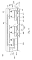
- FIG. 1 A schematic sectional view of a conventional embedded package structure 100 is shown in Fig. 1 , which is a single-chip embedded structure including chips 110, metal layers 120, an insulation material layer 130 and two passivation layers 140.
- the chips 110, the metal layers 120 and an insulation material layer 130 are sandwiched between the passivation layers 140.
- the chips 110 are individually positioned in the insulation material layer 130, and electrically connected to other chips 110 through the metal layers 120.
- the present disclosure provides an embedded package structure and a method for manufacturing thereof.
- the embedded package structure comprises a metal substrate, a chip module, an insulation material layer, and at least one patterned metal layer.
- the metal substrate has a first surface and a second surface.
- the chip module is disposed on the first surface of the metal substrate, and comprises at least two stacked chips being electrically connected to each.
- the insulation material layer covers the first surface of the metal substrate and the stacked chips, and has an electrically interconnection formed therein.
- the patterned metal layer is positioned on the insulation material layer, and is electrically connected the chip module through the electrical interconnection.
- the material of the metal substrate is copper (Cu) or Cu alloy.
- the embedded package structure further comprises another chip module disposed on the first surface of the metal substrate.
- At least one of the chips is of vertical type or lateral type.
- the embedded package structure further comprises an adhesive or a solder positioned between the stacked chips.
- the stacked chips are electrically connected to each other through a conductive layer.
- the material of the insulation material layer includes ABF (Ajinomoto build-up film), BT (bismaleimide-triazine resin), PI (polyimide) or FR4 (glass-epoxy resin).
- ABF Ajinomoto build-up film
- BT bismaleimide-triazine resin
- PI polyimide
- FR4 glass-epoxy resin
- the material of the patterned metal layer is selected from the group consisting of copper (Cu), titanium (Ti), platinum (Pt), aluminum (Al), nickel (Ni), tungsten (W), gold (Au), zinc (Zn), tin (Sn), germanium (Ge), and a combination thereof.
- the embedded package structure further comprises a first passivation layer covering the patterned metal layer.
- the embedded package structure further comprises a second passivation layer covering the second surface of the metal substrate.
- Another embodiment of the present disclosure is to provide a method for manufacturing an embedded package structure.
- the method comprises providing a metal substrate having a first surface and a second surface; forming a chip module disposed on the first surface of the metal substrate, wherein the chip module comprises at least two stacked chips electrically connected to each other; forming an insulation material layer covering the metal substrate and the stacked chips; forming a plurality of vias through the insulation material layers; and forming a patterned metal layer on the insulation material layer, wherein the vias electrically connect the chip module and the patterned metal layer.
- the material of the metal substrate is copper (Cu) or Cu alloy.
- the embedded package structure further includes an adhesive or a solder positioned between the stacked chips.
- the material of the insulation material layer includes ABF (Ajinomoto build-up film), BT (bismaleimide-triazine resin), PI (polyimide) or FR4 (glass-epoxy resin).
- ABF Ajinomoto build-up film
- BT bismaleimide-triazine resin
- PI polyimide
- FR4 glass-epoxy resin
- forming the vias comprises laser drilling, dry etching or wet etching.
- forming the patterned metal layer comprises metalization and etching process.
- the metallization includes physical vapor deposition (PVD), chemical vapor deposition (CVD), atomic layer deposition (ALD) or metal organic chemical vapor deposition (MOCVD).
- PVD physical vapor deposition
- CVD chemical vapor deposition
- ALD atomic layer deposition
- MOCVD metal organic chemical vapor deposition
- the etching process comprises dry etching or wet etching.
- the embedded package structure further comprises a first passivation layer covering the patterned metal layer.
- the embedded package structure further comprises a second passivation layer covering the second surface of the metal substrate.
- the embedded package structure further comprises forming another chip module disposed on the first surface of the metal substrate.
- forming the chip module on the first surface of the metal substrate comprises mounting a first chip on the first surface of the metal substrate; and stacking a second chip on the first chip, wherein the second chip is electrically connected with the first chip.
- forming the chip module on the first surface of the metal substrate comprises providing the chip module comprising at least two stacked chips; and mounting the chip module on the first surface of the metal substrate.
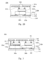
- Fig. 2A is a schematic sectional view of an embedded package structure 200a according to one embodiment of the present disclosure.
- the embedded package structure 200a comprises a metal substrate 210a, a chip module 220a, an insulation material layer 230a, a patterned metal layer 240a, a first passivation layer 251a and a second passivation layer 252a.
- the metal substrate 210a has a first surface 211a and a second surface 212a, and the chip module 220a is disposed on the first surface 211a of the metal substrate 210a.
- the chip module 220a comprises at least two chips vertically integrated and electrically connected to each other. As shown in Fig. 2A , the chip module 220a comprises two stacked chips 221a and 222a, and has a plurality of terminals. In an embodiment, at least one terminal of the chip module 220a is electrically connected to the metal substrate.
- the metal substrate 210a is a lead frame, and the material of the metal substrate 210a is copper (Cu) or Cu alloy.
- At least one of the chips is of vertical type or lateral type.
- both of the chips 221a and 222a are vertical type.
- an adhesive layer or a solder 260a is positioned between the chips 221a and 222a, as shown in Fig. 2A .
- the stacked chips are electrically connected to each other directly or through a conductive layer.
- the chip 221a is directly electrically connected to the chip 222a.
- the insulation material layer 230a has a plurality of vias 231a, and covers the first surface 211a of the metal substrate 210a and the chip module 220a.
- the patterned metal layer 240a is positioned on the insulation material layer 230a, and the vias 231a are electrically connected to at least one terminal of the chip module 220a and the patterned metal layer 240a.
- the material of the insulation material layer includes ABF (Ajinomoto build-up film), BT (bismaleimide-triazine resin), PI (polyimide) or FR4 (glass-epoxy resin), but not to limit.
- ABF Ajinomoto build-up film
- BT bismaleimide-triazine resin
- PI polyimide
- FR4 glass-epoxy resin
- the material of the patterned metal layer is selected by the group of the copper (Cu), titanium (Ti), platinum (Pt), aluminum (Al), nickel (Ni), tungsten (W), gold (Au), zinc (Zn), tin (Sn), germanium (Ge), or a combination thereof.
- the material of the vias 231a is same as the patterned metal layer 240a.
- the material of the vias 231a is different to the patterned metal layer 240a.
- the material of the patterned metal layer 240a is copper (Cu).
- the first passivation layer 251a covers the patterned metal layer 240a.
- the second passivation layer 252a covers the second surface 212a of the metal substrate 210a.
- the material of the first passivation layer is epoxy resins, silicon oxides (SiOx) or silicon nitrides (SiNx).
- the material of the second passivation layer is epoxy resins, silicon oxides (SiOx) or silicon nitrides (SiNx).
- Fig. 2B is a schematic sectional view of an embedded package structure 200b according to one embodiment of the present disclosure.
- the embedded package structure 200b comprises a patterned metal substrate 210b, two chips 221b and 222b, an insulation material layer 230b, a patterned metal layer 240b, a first passivation layer 251b and a second passivation layer 252b.
- the patterned metal substrate 210b has a first surface 211b and a second surface 212b, and the chips 221b and 222b are stacked on the first surface 211b of the metal substrate 210b. And the chip 221b is electrically connected to the chip 222b, which forms a chip module 220b. In which, the chip 221b is mounted onto the patterned metal substrate 210b in a flip-chip manner, and the chip 222b is stacked and electrically connected to the chip 221b. In Fig. 2B , the chip 221b is electrically connected to the chip 222b through a conductive layer 260b, wherein the conductive layer 260b is a solder.
- the insulation material layer 230b has a plurality of vias 231b, and covers the first surface 211b of the metal substrate 210b and the chip 222b.
- the patterned metal layer 240b is positioned on the insulation material layer 230b, and the vias 231b are electrically connected to the chip 222b and the patterned metal layer 240b.
- the first passivation layer 251b covers the patterned metal layer 240b.
- the second passivation layer 252b covers the second surface 212b of the metal substrate 210b.
- Fig. 3 is a schematic sectional view of an embedded package structure 300b according to one embodiment of the present disclosure.
- the an embedded package structure 300b comprises a patterned metal substrate 310, two chip modules 320a and 320b, an insulation material layer 330, a patterned metal layer 340, a first passivation layer 351 and a second passivation layer 352.
- the patterned metal substrate 310 has a first surface 311 and a second surface 312, and the chip modules 320a and 320b are positioned on the first surface 311 of the patterned metal substrate 310.
- the chip module 320a is made by the stacked chips 321a and 322a; and the chip module 320b is made by the stacked chips 321b and 322b.
- an adhesive layer 360a is sandwiched between the stacked chips 321a and 322a of the chip module 320a. And the stacked chips 321a and 322a of the chip module 320a are directly electrically connected to each other; and the stacked chips 321b and 322b of the chip module 320b are electrically connected to each other through a conductive layer 360b.
- the insulation material layer 330 has a plurality of vias 331, and covers the first surface 311 of the patterned metal substrate 310 and the chip modules 320a and 320b.
- the patterned metal layer 340 is positioned on the insulation material layer 330.
- the vias 331 are electrically connected to the chip modules 320a and 320b and the patterned metal layer 340, wherein the chips 321a and 322a of the chip module 320a and the chip 322b of the chip module 320b are electrically connected to the patterned metal layer 340, and the chip 321b of the chip module 320b is electrically connected to the patterned metal substrate 310. And the chip 322a of the chip module 320a is electrically connected to the chip 322b of the chip module 320b through the patterned metal layer 340.
- the chip module further comprises another chip disposed on the patterned metal substrate 310 and electrically connected to other chips, stacked chips, chip modules or a combination thereof through the patterned metal layer.
- Fig. 4 is a schematic sectional view of an embedded package structure 400 according to one embodiment of the present disclosure.
- the embedded package structure 400 comprises a patterned metal substrate 410, chip modules 420a, 420b and 420c, an insulation material layer 430, a first patterned metal layer 441, a second patterned metal layer 442, a third patterned metal layer 443, a first passivation layer 451, a second passivation layer 452, a third passivation layer 453 and a fourth passivation layer 454.
- the patterned metal substrate 410 has a first surface 411 and a second surface 412, and the chip modules 420a, 420b and 420c are positioned on the first surface 411 of the patterned metal substrate 410.
- the chip module 420a is made by the stacked chips 421a and 422a; the chip module 420b is made by the stacked chips 421b and 422b; and the chip module 420c is made by the stacked chips 421c and 422c.
- an adhesive layer 460a is sandwiched between the stacked chips 421a and 422a of the chip module 420a. And the stacked chips 421a and 422a of the chip module 420a are directly electrically connected to each other.
- the stacked chips 421b and 422b of the chip module 420b are electrically connected to each other through a conductive layer 460b; and the stacked chips 421c and 422c of the chip module 420c are electrically connected to each other through a conductive layer 460c.
- the insulation material layer 430 has a plurality of vias 431, and covers the first surface 411 of the patterned metal substrate 410 and the chip modules 420a, 420b and 420c.
- the first patterned metal layer 441, the first passivation layer 451, the second patterned metal layer 442 and the second passivation layer 452 are sequentially positioned on the insulation material layer 430.
- the vias 431 are electrically connected to the chip modules 420a, 420b and 420c, and the first patterned metal layer 441.
- the chips 421a and 422a of the chip module 420a, the chip 422b of the chip module 420b and the chip 422c of the chip module 420c are electrically connected to the first patterned metal layer 441.
- the chip 421b of the chip module 420b and the chip 421c of the chip module 420c are flip chips electrically connected to the patterned metal substrate 410.
- the chip 422a of the chip module 420a is electrically connected to the chip 422b of the chip module 420b through the first patterned metal layer 441. And the chip 422a of the chip module 420a is electrically connected to the chip 422c of the chip module 420c through the second patterned metal layer 442.
- the third passivation layer 453, the third patterned metal layer 443 and the fourth passivation layer 454 are sequentially positioned on the second surface 412 of the patterned metal substrate 410.
- the chip 421b of the chip module 420b is electrically connected to the chip 421c of the chip module 420c through the third patterned metal layer 443.
- Fig. 5A to 5F are schematic sectional views of making an embedded package structure 500 according to one embodiment of the present disclosure.
- a metal substrate 510 is provided, which has a first surface 511 and a second surface 512.
- the material of the metal substrate is copper (Cu) or Cu alloy.
- the chip modules 520a and 520b are positioned on the first surface 511 of the metal substrate 510.
- the chips 521a and 522a are stacked to form the chip module 520a, and directly electrically connected to each other.
- forming the chip module on the first surface of the metal substrate comprises mounting a first chip on the first surface of the metal substrate, and stacking a second chip on the first chip, wherein the second chip is electrically connected with the first chip.
- forming the chip module on the first surface of the metal substrate comprises providing the chip module comprising at least two stacked chips, and mounting the chip module on the first surface of the metal substrate. And an adhesive layer 523a is sandwiched between the stacked chips 521a and 522a.
- the chips 521b and 522b are stacked to form the chip module 520b, and electrically connected to each other through a conductive layer 523b, wherein the conductive layer 523b is a solder or adhesive material.
- the chip 521b is flip-chip mounted on the metal substrate 510.
- the chip 522a can be vertically integrated and electrically connected to the chip 521a before or after mounting the chip 521a on the metal substrate 510.
- the chip 522a is stacked on the chip 521a after the chip 521a is mounted on the metal substrate 510.
- the chip module 520a is first formed and then mounted on the metal substrate 510.
- an insulation material layer 530 covers the first surface 511 of the metal substrate 510 and the chip modules 520a and 520b.
- the material of the insulation material layer includes ABF (Ajinomoto build-up film), BT (bismaleimide-triazine resin), PI (polyimide) or FR4 (glass-epoxy resin).
- the step of forming the vias comprises performing laser drilling, dry etching or wet etching process to form a plurality of via holes, and then filling a conductive layer into the via holes to form the vias.
- a patterned metal layer 540 is formed on the insulation material layer 530 including the vias 531.
- the step of forming the patterned metal layer 540 comprises metallization and etching process, wherein the metallization includes physical vapor deposition (PVD), chemical vapor deposition (CVD), atomic layer deposition (ALD) or metal organic chemical vapor deposition (MOCVD); and the etching process is dry etching or wet etching.
- the metal substrate 510 is patterned by the etching process in the step of forming the patterned metal layer.
- the material of the patterned metal layer 540 is selected from the group of copper (Cu), titanium (Ti), platinum (Pt), aluminum (Al), nickel (Ni), tungsten (W), gold (Au), zinc (Zn), tin (Sn), germanium (Ge), or a combination thereof.
- the material of the vias 531 is same as the patterned metal layer 540.
- the material of the vias 531 is different to the patterned metal layer 540.
- the chip modules 520a and 520b are electrically connected to the patterned metal layer through vias 540, in which the chip 522a of the chip module 520a is electrically connected to the chip 522b of the chip module 520b through the patterned metal layer 540.
- the stacked chips are laterally disposed to form the chip module, and then the chip module is electrically connected to other chips, stacked chips, chip modules or a combination thereof through the patterned metal layer.
- the step of forming the first passivation layer and the second passivation layer is deposition or coating.
- the material of the first passivation layer is epoxy resins, silicon oxides (SiOx) or silicon nitrides (SiNx).
- the material of the second passivation layer is epoxy resins, silicon oxides (SiOx) or silicon nitrides (SiNx).
- the present disclosure provides an improved embedded package structure having at least two stacked chips.
- the stacked chips are electrically connected to each other directly or through a conductive layer, and forms a chip module in the embedded package structure.
- the embedded package structure according to the present disclosure is simplified the design of the redistribution layer thereof, and has a shorter signal transmission distance between chips or chip modules, so as to improve parasitic effects of embedded package structures and shrink the size of the embedded package structure. Otherwise, due to the design of the simplified redistribution layer, the embedded package structure is not only reduced parasitic effects, but also increased the power density and the reliability thereof.
- the production cost of the embedded package structure according to the present disclosure is relatively lower than the conventional embedded package structure.
Landscapes
- Production Of Multi-Layered Print Wiring Board (AREA)
- Internal Circuitry In Semiconductor Integrated Circuit Devices (AREA)
Abstract
The disclosure provides an embedded package structure comprising a metal substrate (210a), a chip module (220a), an insulation material layer (230a), and at least one patterned metal layer (240a). The metal substrate (210a) has a first surface (211a) and a second surface (212a). The chip module (220a) is disposed on the first surface of the metal substrate, and comprises at least two stacked chips (222a,221a) being electrically connected to each. The insulation material layer (230a) covers the first surface of the metal substrate and the stacked chips and has an electrical interconnection (231a) formed therein. The patterned metal layer (240a) is positioned on the insulation material layer, and is electrically connected the chip module through the electrical interconnection. The method for manufacturing the embedded package structure is also disclosed.
Description
- The present disclosure relates to a package structure, and more particularly, to an embedded package structure.
- A schematic sectional view of a conventional embedded
package structure 100 is shown inFig. 1 , which is a single-chip embeddedstructure including chips 110,metal layers 120, aninsulation material layer 130 and twopassivation layers 140. - As shown In
Fig. 1 , thechips 110, themetal layers 120 and aninsulation material layer 130 are sandwiched between thepassivation layers 140. Thechips 110 are individually positioned in theinsulation material layer 130, and electrically connected toother chips 110 through themetal layers 120. - Since there are the numerous metal routing layers connecting to the chips, parasitic effects may appear in the embedded package structure to damage the chips. Besides, due to the numerous metal routing layers, the signal transmission distance in the single-chip embedded structure is so long that the intensity and quality of the signal may deteriorate. On the other way, the conventional embedded package structure having lots of chips inside always has a large size, which is unfavorable in design of a compact device.
- Therefore, there is a need for an improved embedded package structure and a method for manufacturing the same, so as to solve the problems met in the art.
- The present disclosure provides an embedded package structure and a method for manufacturing thereof.
- One embodiment of the present disclosure is to provide an embedded package structure. The embedded package structure comprises a metal substrate, a chip module, an insulation material layer, and at least one patterned metal layer.
- The metal substrate has a first surface and a second surface.
- The chip module is disposed on the first surface of the metal substrate, and comprises at least two stacked chips being electrically connected to each.
- The insulation material layer covers the first surface of the metal substrate and the stacked chips, and has an electrically interconnection formed therein.
- The patterned metal layer is positioned on the insulation material layer, and is electrically connected the chip module through the electrical interconnection.
- According to one example of the present disclosure, the material of the metal substrate is copper (Cu) or Cu alloy.
- According to one example of the present disclosure, the embedded package structure further comprises another chip module disposed on the first surface of the metal substrate.
- According to one example of the present disclosure, at least one of the chips is of vertical type or lateral type.
- According to one example of the present disclosure, the embedded package structure further comprises an adhesive or a solder positioned between the stacked chips.
- According to one example of the present disclosure, the stacked chips are electrically connected to each other through a conductive layer.
- According to one example of the present disclosure, the material of the insulation material layer includes ABF (Ajinomoto build-up film), BT (bismaleimide-triazine resin), PI (polyimide) or FR4 (glass-epoxy resin).
- According to one example of the present disclosure, the material of the patterned metal layer is selected from the group consisting of copper (Cu), titanium (Ti), platinum (Pt), aluminum (Al), nickel (Ni), tungsten (W), gold (Au), zinc (Zn), tin (Sn), germanium (Ge), and a combination thereof.
- According to one example of the present disclosure, the embedded package structure further comprises a first passivation layer covering the patterned metal layer.
- According to one example of the present disclosure, the embedded package structure further comprises a second passivation layer covering the second surface of the metal substrate.
- Another embodiment of the present disclosure is to provide a method for manufacturing an embedded package structure. The method comprises providing a metal substrate having a first surface and a second surface; forming a chip module disposed on the first surface of the metal substrate, wherein the chip module comprises at least two stacked chips electrically connected to each other; forming an insulation material layer covering the metal substrate and the stacked chips; forming a plurality of vias through the insulation material layers; and forming a patterned metal layer on the insulation material layer, wherein the vias electrically connect the chip module and the patterned metal layer.
- According to one example of the present disclosure, the material of the metal substrate is copper (Cu) or Cu alloy.
- According to one example of the present disclosure, the embedded package structure further includes an adhesive or a solder positioned between the stacked chips.
- According to one example of the present disclosure, the material of the insulation material layer includes ABF (Ajinomoto build-up film), BT (bismaleimide-triazine resin), PI (polyimide) or FR4 (glass-epoxy resin).
- According to one example of the present disclosure, forming the vias comprises laser drilling, dry etching or wet etching.
- According to one example of the present disclosure, forming the patterned metal layer comprises metalization and etching process.
- According to one example of the present disclosure, the metallization includes physical vapor deposition (PVD), chemical vapor deposition (CVD), atomic layer deposition (ALD) or metal organic chemical vapor deposition (MOCVD).
- According to one example of the present disclosure, the etching process comprises dry etching or wet etching.
- According to one example of the present disclosure, the embedded package structure further comprises a first passivation layer covering the patterned metal layer.
- According to one example of the present disclosure, the embedded package structure further comprises a second passivation layer covering the second surface of the metal substrate.
- According to one example of the present disclosure, the embedded package structure further comprises forming another chip module disposed on the first surface of the metal substrate.
- According to one example of the present disclosure, forming the chip module on the first surface of the metal substrate comprises mounting a first chip on the first surface of the metal substrate; and stacking a second chip on the first chip, wherein the second chip is electrically connected with the first chip.
- According to one example of the present disclosure, forming the chip module on the first surface of the metal substrate comprises providing the chip module comprising at least two stacked chips; and mounting the chip module on the first surface of the metal substrate.
- For a more complete understanding of the present invention, and the advantages thereof, reference is now made to the following descriptions taken in conjunction with the accompanying drawings, in which:
-
Fig. 1 is a schematic sectional view of a conventional embeddedpackage structure 100; -
Fig. 2A is a schematic sectional view of an embeddedpackage structure 200a according to one embodiment of the present disclosure; -
Fig. 2B is a schematic sectional view of an embeddedpackage structure 200b according to one embodiment of the present disclosure; -
Fig. 3 is a schematic sectional view of an embedded package structure 300 according to one embodiment of the present disclosure; -
Fig. 4 is a schematic sectional view of an embeddedpackage structure 400 according to one embodiment of the present disclosure; and -
Fig. 5A to 5F are schematic sectional views of making an embeddedpackage structure 500 according to one embodiment of the present disclosure. - The embodiments of the embedded package structure and a method for manufacturing the same of the present disclosure are discussed in detail below, but not limited the scope of the present disclosure. The same symbols or numbers are used to the same or similar portion in the drawings or the description. And the applications of the present disclosure are not limited by the following embodiments and examples which the person in the art can apply in the related field.
-
Fig. 2A is a schematic sectional view of an embeddedpackage structure 200a according to one embodiment of the present disclosure. InFig. 2A , the embeddedpackage structure 200a comprises ametal substrate 210a, achip module 220a, aninsulation material layer 230a, a patternedmetal layer 240a, afirst passivation layer 251a and asecond passivation layer 252a. - The
metal substrate 210a has afirst surface 211a and asecond surface 212a, and thechip module 220a is disposed on thefirst surface 211a of themetal substrate 210a. Thechip module 220a comprises at least two chips vertically integrated and electrically connected to each other. As shown inFig. 2A , thechip module 220a comprises two stackedchips chip module 220a is electrically connected to the metal substrate. According to one example of the present disclosure, themetal substrate 210a is a lead frame, and the material of themetal substrate 210a is copper (Cu) or Cu alloy. - According to one example of the present disclosure, at least one of the chips is of vertical type or lateral type. In
Fig. 2A , both of thechips - According to one example of the present disclosure, an adhesive layer or a
solder 260a is positioned between thechips Fig. 2A . - According to one example of the present disclosure, the stacked chips are electrically connected to each other directly or through a conductive layer. In an embodiment, the
chip 221a is directly electrically connected to thechip 222a. - The
insulation material layer 230a has a plurality of vias 231a, and covers thefirst surface 211a of themetal substrate 210a and thechip module 220a. The patternedmetal layer 240a is positioned on theinsulation material layer 230a, and thevias 231a are electrically connected to at least one terminal of thechip module 220a and the patternedmetal layer 240a. - According to one example of the present disclosure, the material of the insulation material layer includes ABF (Ajinomoto build-up film), BT (bismaleimide-triazine resin), PI (polyimide) or FR4 (glass-epoxy resin), but not to limit. In
Fig. 2A , theinsulation material layer 230a is made from ABF. - According to one example of the present disclosure, the material of the patterned metal layer is selected by the group of the copper (Cu), titanium (Ti), platinum (Pt), aluminum (Al), nickel (Ni), tungsten (W), gold (Au), zinc (Zn), tin (Sn), germanium (Ge), or a combination thereof. According to one example of the disclosure, the material of the vias 231a is same as the patterned
metal layer 240a. According to another example of the disclosure, the material of the vias 231a is different to the patternedmetal layer 240a. InFig. 2A , the material of the patternedmetal layer 240a is copper (Cu). - The
first passivation layer 251a covers the patternedmetal layer 240a. And thesecond passivation layer 252a covers thesecond surface 212a of themetal substrate 210a. According to one example of the present disclosure, the material of the first passivation layer is epoxy resins, silicon oxides (SiOx) or silicon nitrides (SiNx). According to one example of the present disclosure, the material of the second passivation layer is epoxy resins, silicon oxides (SiOx) or silicon nitrides (SiNx). -
Fig. 2B is a schematic sectional view of an embeddedpackage structure 200b according to one embodiment of the present disclosure. InFig. 2B , the embeddedpackage structure 200b comprises a patternedmetal substrate 210b, twochips insulation material layer 230b, a patternedmetal layer 240b, afirst passivation layer 251b and asecond passivation layer 252b. - The patterned
metal substrate 210b has afirst surface 211b and asecond surface 212b, and thechips first surface 211b of themetal substrate 210b. And thechip 221b is electrically connected to thechip 222b, which forms achip module 220b. In which, thechip 221b is mounted onto the patternedmetal substrate 210b in a flip-chip manner, and thechip 222b is stacked and electrically connected to thechip 221b. InFig. 2B , thechip 221b is electrically connected to thechip 222b through aconductive layer 260b, wherein theconductive layer 260b is a solder. - The
insulation material layer 230b has a plurality ofvias 231b, and covers thefirst surface 211b of themetal substrate 210b and thechip 222b. The patternedmetal layer 240b is positioned on theinsulation material layer 230b, and thevias 231b are electrically connected to thechip 222b and the patternedmetal layer 240b. - The
first passivation layer 251b covers the patternedmetal layer 240b. And thesecond passivation layer 252b covers thesecond surface 212b of themetal substrate 210b. -
Fig. 3 is a schematic sectional view of an embeddedpackage structure 300b according to one embodiment of the present disclosure. InFig. 3 , the an embeddedpackage structure 300b comprises a patternedmetal substrate 310, twochip modules insulation material layer 330, a patternedmetal layer 340, afirst passivation layer 351 and asecond passivation layer 352. - The patterned
metal substrate 310 has afirst surface 311 and asecond surface 312, and thechip modules first surface 311 of the patternedmetal substrate 310. In which, thechip module 320a is made by the stackedchips chip module 320b is made by the stackedchips - In
Fig. 3 , anadhesive layer 360a is sandwiched between thestacked chips chip module 320a. And thestacked chips chip module 320a are directly electrically connected to each other; and thestacked chips chip module 320b are electrically connected to each other through aconductive layer 360b. - The
insulation material layer 330 has a plurality ofvias 331, and covers thefirst surface 311 of the patternedmetal substrate 310 and thechip modules metal layer 340 is positioned on theinsulation material layer 330. - In
Fig. 3 , thevias 331 are electrically connected to thechip modules metal layer 340, wherein thechips chip module 320a and thechip 322b of thechip module 320b are electrically connected to the patternedmetal layer 340, and thechip 321b of thechip module 320b is electrically connected to the patternedmetal substrate 310. And thechip 322a of thechip module 320a is electrically connected to thechip 322b of thechip module 320b through the patternedmetal layer 340. - According to one example of the present disclosure, the chip module further comprises another chip disposed on the patterned
metal substrate 310 and electrically connected to other chips, stacked chips, chip modules or a combination thereof through the patterned metal layer. -
Fig. 4 is a schematic sectional view of an embeddedpackage structure 400 according to one embodiment of the present disclosure. InFig. 4 , the embeddedpackage structure 400 comprises a patternedmetal substrate 410,chip modules insulation material layer 430, a firstpatterned metal layer 441, a secondpatterned metal layer 442, a thirdpatterned metal layer 443, afirst passivation layer 451, asecond passivation layer 452, athird passivation layer 453 and afourth passivation layer 454. - The patterned
metal substrate 410 has afirst surface 411 and asecond surface 412, and thechip modules first surface 411 of the patternedmetal substrate 410. In which, thechip module 420a is made by the stackedchips chip module 420b is made by the stackedchips chip module 420c is made by the stackedchips - In
Fig. 4 , anadhesive layer 460a is sandwiched between thestacked chips chip module 420a. And thestacked chips chip module 420a are directly electrically connected to each other. Thestacked chips chip module 420b are electrically connected to each other through aconductive layer 460b; and thestacked chips chip module 420c are electrically connected to each other through aconductive layer 460c. - The
insulation material layer 430 has a plurality ofvias 431, and covers thefirst surface 411 of the patternedmetal substrate 410 and thechip modules patterned metal layer 441, thefirst passivation layer 451, the secondpatterned metal layer 442 and thesecond passivation layer 452 are sequentially positioned on theinsulation material layer 430. - In
Fig. 4 , thevias 431 are electrically connected to thechip modules patterned metal layer 441. In which, thechips chip module 420a, thechip 422b of thechip module 420b and thechip 422c of thechip module 420c are electrically connected to the firstpatterned metal layer 441. And thechip 421b of thechip module 420b and thechip 421c of thechip module 420c are flip chips electrically connected to the patternedmetal substrate 410. - The
chip 422a of thechip module 420a is electrically connected to thechip 422b of thechip module 420b through the firstpatterned metal layer 441. And thechip 422a of thechip module 420a is electrically connected to thechip 422c of thechip module 420c through the secondpatterned metal layer 442. - The
third passivation layer 453, the thirdpatterned metal layer 443 and thefourth passivation layer 454 are sequentially positioned on thesecond surface 412 of the patternedmetal substrate 410. In which, thechip 421b of thechip module 420b is electrically connected to thechip 421c of thechip module 420c through the thirdpatterned metal layer 443. -
Fig. 5A to 5F are schematic sectional views of making an embeddedpackage structure 500 according to one embodiment of the present disclosure. InFig. 5A , ametal substrate 510 is provided, which has afirst surface 511 and asecond surface 512. According to one example of the present disclosure, the material of the metal substrate is copper (Cu) or Cu alloy. - Then, as shown in
Fig. 5B , thechip modules first surface 511 of themetal substrate 510. In which, thechips chip module 520a, and directly electrically connected to each other. According to one embodiment of the present disclosure, forming the chip module on the first surface of the metal substrate comprises mounting a first chip on the first surface of the metal substrate, and stacking a second chip on the first chip, wherein the second chip is electrically connected with the first chip. According to another embodiment of the present disclosure, forming the chip module on the first surface of the metal substrate comprises providing the chip module comprising at least two stacked chips, and mounting the chip module on the first surface of the metal substrate. And anadhesive layer 523a is sandwiched between thestacked chips - The
chips chip module 520b, and electrically connected to each other through aconductive layer 523b, wherein theconductive layer 523b is a solder or adhesive material. InFig. 5B , thechip 521b is flip-chip mounted on themetal substrate 510. According to the present invention, thechip 522a can be vertically integrated and electrically connected to thechip 521a before or after mounting thechip 521a on themetal substrate 510. - In one embodiment of the present disclosure, the
chip 522a is stacked on thechip 521a after thechip 521a is mounted on themetal substrate 510. In another embodiment of the present disclosure, thechip module 520a is first formed and then mounted on themetal substrate 510. InFig. 5C , aninsulation material layer 530 covers thefirst surface 511 of themetal substrate 510 and thechip modules - Then, a plurality of
vias 531 are formed in theinsulation material layer 530, as shown inFig. 5D . According to one example of the present disclosure, the step of forming the vias comprises performing laser drilling, dry etching or wet etching process to form a plurality of via holes, and then filling a conductive layer into the via holes to form the vias. - In
Fig. 5E , a patternedmetal layer 540 is formed on theinsulation material layer 530 including thevias 531. According to one example of the present disclosure, the step of forming the patternedmetal layer 540 comprises metallization and etching process, wherein the metallization includes physical vapor deposition (PVD), chemical vapor deposition (CVD), atomic layer deposition (ALD) or metal organic chemical vapor deposition (MOCVD); and the etching process is dry etching or wet etching. According to another example of the present disclosure, themetal substrate 510 is patterned by the etching process in the step of forming the patterned metal layer. - The material of the patterned
metal layer 540 is selected from the group of copper (Cu), titanium (Ti), platinum (Pt), aluminum (Al), nickel (Ni), tungsten (W), gold (Au), zinc (Zn), tin (Sn), germanium (Ge), or a combination thereof. According to one example of the disclosure, the material of thevias 531 is same as the patternedmetal layer 540. According to another example of the disclosure, the material of thevias 531 is different to the patternedmetal layer 540. - The
chip modules vias 540, in which thechip 522a of thechip module 520a is electrically connected to thechip 522b of thechip module 520b through the patternedmetal layer 540. According to one example of the present disclosure, the stacked chips are laterally disposed to form the chip module, and then the chip module is electrically connected to other chips, stacked chips, chip modules or a combination thereof through the patterned metal layer. - Then, a
first passivation layer 551 is formed on the patternedmetal layer 540, and asecond passivation layer 552 is formed on thesecond surface 512 of themetal substrate 510. And the embeddedpackage structure 500 is thereby completed as shown inFig. 5F . According to one example of the present disclosure, the step of forming the first passivation layer and the second passivation layer is deposition or coating. According to one example of the present disclosure, the material of the first passivation layer is epoxy resins, silicon oxides (SiOx) or silicon nitrides (SiNx). According to another example of the present disclosure, the material of the second passivation layer is epoxy resins, silicon oxides (SiOx) or silicon nitrides (SiNx). - The present disclosure provides an improved embedded package structure having at least two stacked chips. In which, the stacked chips are electrically connected to each other directly or through a conductive layer, and forms a chip module in the embedded package structure. Unlike to the conventional embedded package structure, the embedded package structure according to the present disclosure is simplified the design of the redistribution layer thereof, and has a shorter signal transmission distance between chips or chip modules, so as to improve parasitic effects of embedded package structures and shrink the size of the embedded package structure. Otherwise, due to the design of the simplified redistribution layer, the embedded package structure is not only reduced parasitic effects, but also increased the power density and the reliability thereof. The production cost of the embedded package structure according to the present disclosure is relatively lower than the conventional embedded package structure.
Claims (20)
- An embedded package structure comprising:a metal substrate having a first surface and a second surface;a chip module, disposed on the first surface of the metal substrate, comprising at least two stacked chips being electrically connected to each;an insulation material layer covering the first surface of the metal substrate and the chip module and having an electrical interconnection formed therein; andat least one patterned metal layer, positioned on the insulation material layer, electrically connected the chip module through the electrical interconnection.
- The embedded package structure of claim 1, further comprising another chip module disposed on the first surface of the metal substrate.
- The embedded package structure of claim 1, wherein at least one of the chips is of vertical type or lateral type.
- The embedded package structure of claim 1, further comprising an adhesive layer or a solder positioned between the stacked chips.
- The embedded package structure of claim 1, wherein the stacked chips are electrically connected to each other through a conductive layer.
- The embedded package structure of claim 1, wherein the material of the insulation material layer comprises ABF (Ajinomoto build-up film), BT (bismaleimide-triazine resin), PI (polyimide) or FR4 (glass-epoxy resin).
- The embedded package structure of claim 1, wherein the material of the patterned metal layer is selected from the group consisting of copper (Cu), titanium (Ti), platinum (Pt), aluminum (Al), nickel (Ni), tungsten (W), gold (Au), zinc (Zn), tin (Sn), germanium (Ge), and a combination thereof.
- The embedded package structure of claim 1, further comprising a first passivation layer covering the patterned metal layer.
- The embedded package structure of claim 8, further comprising a second passivation layer covering the second surface of the metal substrate.
- A method for manufacturing an embedded package structure, comprising the steps of:providing a metal substrate having a first surface and a second surface;forming a chip module disposed on the first surface of the metal substrate, wherein the chip module comprises at least two stacked chips electrically connected to each other;forming an insulation material layer covering the first substrate of the metal substrate and the chip module;forming a plurality of vias through the insulation material layer; andforming at least one patterned metal layer on the insulation material layer, wherein the vias electrically connect the chip module and the patterned metal layer.
- The method of claim 10, wherein the material of the metal substrate is copper (Cu) and Cu alloy.
- The method of claim 10, further comprising an adhesive layer or a solder positioned between the stacked chips.
- The method of claim 10, wherein the material of the insulation material layer comprises ABF (Ajinomoto build-up film), BT (bismaleimide-triazine resin), PI (polyimide) or FR4 (glass-epoxy resin).
- The method of claim 10, wherein forming the vias comprises performing a laser drilling, dry etching, or wet etching process to form a plurality of via holes.
- The method of claim 10, wherein forming the patterned metal layer comprises metallization and etching process.
- The method of claim 15, wherein the metallization comprises physical vapor deposition (PVD), chemical vapor deposition (CVD), atomic layer deposition (ALD) or metal organic chemical vapor deposition (MOCVD).
- The method of claim 15, wherein the etching process comprises dry etching or wet etching.
- The method of claim 10, further comprising forming another chip module disposed on the first surface of the metal substrate.
- The method of claim 10, wherein forming the chip module on the first surface of the metal substrate comprises:mounting a first chip on the first surface of the metal substrate; andstacking a second chip on the first chip, wherein the second chip is electrically connected with the first chip.
- The method of claim 10, wherein forming the chip module on the first surface of the metal substrate comprises:providing the chip module comprising at least two stacked chips; andmounting the chip module on the first surface of the metal substrate.
Priority Applications (1)
| Application Number | Priority Date | Filing Date | Title |
|---|---|---|---|
| EP14197415.4A EP2881985A1 (en) | 2013-06-28 | 2013-09-09 | Embedded package structure and method for manufacturing thereof |
Applications Claiming Priority (1)
| Application Number | Priority Date | Filing Date | Title |
|---|---|---|---|
| US13/930,949 US8912663B1 (en) | 2013-06-28 | 2013-06-28 | Embedded package structure and method for manufacturing thereof |
Related Child Applications (1)
| Application Number | Title | Priority Date | Filing Date |
|---|---|---|---|
| EP14197415.4A Division EP2881985A1 (en) | 2013-06-28 | 2013-09-09 | Embedded package structure and method for manufacturing thereof |
Publications (1)
| Publication Number | Publication Date |
|---|---|
| EP2819157A1 true EP2819157A1 (en) | 2014-12-31 |
Family
ID=49123749
Family Applications (2)
| Application Number | Title | Priority Date | Filing Date |
|---|---|---|---|
| EP13183564.7A Withdrawn EP2819157A1 (en) | 2013-06-28 | 2013-09-09 | Embedded package structure and method for manufacturing thereof |
| EP14197415.4A Ceased EP2881985A1 (en) | 2013-06-28 | 2013-09-09 | Embedded package structure and method for manufacturing thereof |
Family Applications After (1)
| Application Number | Title | Priority Date | Filing Date |
|---|---|---|---|
| EP14197415.4A Ceased EP2881985A1 (en) | 2013-06-28 | 2013-09-09 | Embedded package structure and method for manufacturing thereof |
Country Status (4)
| Country | Link |
|---|---|
| US (1) | US8912663B1 (en) |
| EP (2) | EP2819157A1 (en) |
| CN (1) | CN104253114A (en) |
| TW (1) | TWI488269B (en) |
Families Citing this family (10)
| Publication number | Priority date | Publication date | Assignee | Title |
|---|---|---|---|---|
| EP2881983B1 (en) * | 2013-12-05 | 2019-09-18 | ams AG | Interposer-chip-arrangement for dense packaging of chips |
| CN103730379A (en) * | 2014-01-16 | 2014-04-16 | 苏州晶方半导体科技股份有限公司 | Chip packaging method and structure |
| CN104795380A (en) * | 2015-03-27 | 2015-07-22 | 江阴长电先进封装有限公司 | Three-dimensional packaging structure |
| US9543270B1 (en) | 2015-07-31 | 2017-01-10 | Inotera Memories, Inc. | Multi-device package and manufacturing method thereof |
| DE102016104284B4 (en) | 2016-03-09 | 2022-05-12 | Semikron Elektronik Gmbh & Co. Kg | Encapsulated power semiconductor device with a shaped metal body as the first connection conductor |
| US10204884B2 (en) * | 2016-06-29 | 2019-02-12 | Intel Corporation | Multichip packaging for dice of different sizes |
| KR101872619B1 (en) * | 2016-11-17 | 2018-06-28 | 삼성전기주식회사 | Fan-out semiconductor package |
| US10600679B2 (en) | 2016-11-17 | 2020-03-24 | Samsung Electronics Co., Ltd. | Fan-out semiconductor package |
| KR101983186B1 (en) | 2016-12-16 | 2019-05-28 | 삼성전기주식회사 | Fan-out semiconductor package |
| US20250309192A1 (en) * | 2024-03-29 | 2025-10-02 | Intel Corporation | 3d die stacking with hybrid bonding and through dielectric via structures |
Citations (2)
| Publication number | Priority date | Publication date | Assignee | Title |
|---|---|---|---|---|
| US20080217761A1 (en) * | 2007-03-08 | 2008-09-11 | Advanced Chip Engineering Technology Inc. | Structure of semiconductor device package and method of the same |
| JP2009033185A (en) * | 2008-09-05 | 2009-02-12 | Sanyo Electric Co Ltd | Semiconductor device and manufacturing method thereof |
Family Cites Families (14)
| Publication number | Priority date | Publication date | Assignee | Title |
|---|---|---|---|---|
| JP2001168264A (en) * | 1999-12-13 | 2001-06-22 | Hitachi Ltd | Electronic circuit module and method of manufacturing the same |
| JP2003051569A (en) * | 2001-08-03 | 2003-02-21 | Seiko Epson Corp | Semiconductor device and manufacturing method thereof |
| FI119215B (en) | 2002-01-31 | 2008-08-29 | Imbera Electronics Oy | Method of inserting a component into a base material and electronics module |
| JP4535002B2 (en) | 2005-09-28 | 2010-09-01 | Tdk株式会社 | Semiconductor IC-embedded substrate and manufacturing method thereof |
| KR101557273B1 (en) | 2009-03-17 | 2015-10-05 | 삼성전자주식회사 | Semiconductor package |
| TWI362102B (en) | 2007-07-11 | 2012-04-11 | Ind Tech Res Inst | Three-dimensional dice-stacking package structure and method for manufactruing the same |
| US8049320B2 (en) | 2008-02-19 | 2011-11-01 | Texas Instruments Incorporated | Integrated circuit stacked package precursors and stacked packaged devices and systems therefrom |
| KR101501739B1 (en) * | 2008-03-21 | 2015-03-11 | 삼성전자주식회사 | Method of Fabricating Semiconductor Packages |
| US8105915B2 (en) * | 2009-06-12 | 2012-01-31 | Stats Chippac, Ltd. | Semiconductor device and method of forming vertical interconnect structure between non-linear portions of conductive layers |
| US8238113B2 (en) * | 2010-07-23 | 2012-08-07 | Imbera Electronics Oy | Electronic module with vertical connector between conductor patterns |
| US8518746B2 (en) * | 2010-09-02 | 2013-08-27 | Stats Chippac, Ltd. | Semiconductor device and method of forming TSV semiconductor wafer with embedded semiconductor die |
| KR101207273B1 (en) * | 2010-09-03 | 2012-12-03 | 에스케이하이닉스 주식회사 | Embedded package and method for forming the same |
| US8860079B2 (en) * | 2010-11-15 | 2014-10-14 | United Test And Assembly Center Ltd. | Semiconductor packages and methods of packaging semiconductor devices |
| US8866302B2 (en) * | 2011-01-25 | 2014-10-21 | Infineon Technologies Ag | Device including two semiconductor chips and manufacturing thereof |
-
2013
- 2013-06-28 US US13/930,949 patent/US8912663B1/en active Active
- 2013-09-06 TW TW102132089A patent/TWI488269B/en active
- 2013-09-09 EP EP13183564.7A patent/EP2819157A1/en not_active Withdrawn
- 2013-09-09 EP EP14197415.4A patent/EP2881985A1/en not_active Ceased
- 2013-09-11 CN CN201310412949.8A patent/CN104253114A/en active Pending
Patent Citations (2)
| Publication number | Priority date | Publication date | Assignee | Title |
|---|---|---|---|---|
| US20080217761A1 (en) * | 2007-03-08 | 2008-09-11 | Advanced Chip Engineering Technology Inc. | Structure of semiconductor device package and method of the same |
| JP2009033185A (en) * | 2008-09-05 | 2009-02-12 | Sanyo Electric Co Ltd | Semiconductor device and manufacturing method thereof |
Also Published As
| Publication number | Publication date |
|---|---|
| EP2881985A1 (en) | 2015-06-10 |
| TWI488269B (en) | 2015-06-11 |
| TW201501247A (en) | 2015-01-01 |
| US8912663B1 (en) | 2014-12-16 |
| CN104253114A (en) | 2014-12-31 |
| US20150001727A1 (en) | 2015-01-01 |
Similar Documents
| Publication | Publication Date | Title |
|---|---|---|
| EP2881985A1 (en) | Embedded package structure and method for manufacturing thereof | |
| US9461020B2 (en) | Semiconductor package including an embedded surface mount device and method of forming the same | |
| CN107978583B (en) | Package structure and method for manufacturing the same | |
| CN109216296B (en) | Semiconductor package and method | |
| US10163872B2 (en) | Semiconductor packages and methods of forming the same | |
| CN103681607B (en) | Semiconductor devices and preparation method thereof | |
| US9275929B2 (en) | Package assembly having a semiconductor substrate | |
| KR100871382B1 (en) | Through-silicon via stack package and manufacturing method thereof | |
| CN107808856B (en) | Semiconductor package structure and manufacturing method thereof | |
| US7993976B2 (en) | Semiconductor device and method of forming conductive vias with trench in saw street | |
| CN109786360B (en) | Semiconductor package and method | |
| US20120273941A1 (en) | Package structure having embedded electronic component and fabrication method thereof | |
| US20130026609A1 (en) | Package assembly including a semiconductor substrate with stress relief structure | |
| TW201701404A (en) | Package structure and packaging method | |
| US20120181562A1 (en) | Package having a light-emitting element and method of fabricating the same | |
| CN112713097B (en) | Antenna packaging structure and packaging method | |
| KR102422244B1 (en) | Semiconductor device including a through-via electrode and fabrication method thereof | |
| CN106898625A (en) | The encapsulating structure and method for packing of image sensor chip | |
| CN112713098B (en) | Antenna packaging structure and packaging method | |
| CN109817530B (en) | Packaging assembly manufacturing method | |
| US8076775B2 (en) | Semiconductor package and method for making the same | |
| CN116504648A (en) | Semiconductor device and method using attached | |
| KR20090076357A (en) | Stacked package and its manufacturing method |
Legal Events
| Date | Code | Title | Description |
|---|---|---|---|
| PUAI | Public reference made under article 153(3) epc to a published international application that has entered the european phase |
Free format text: ORIGINAL CODE: 0009012 |
|
| 17P | Request for examination filed |
Effective date: 20130909 |
|
| AK | Designated contracting states |
Kind code of ref document: A1 Designated state(s): AL AT BE BG CH CY CZ DE DK EE ES FI FR GB GR HR HU IE IS IT LI LT LU LV MC MK MT NL NO PL PT RO RS SE SI SK SM TR |
|
| AX | Request for extension of the european patent |
Extension state: BA ME |
|
| STAA | Information on the status of an ep patent application or granted ep patent |
Free format text: STATUS: THE APPLICATION HAS BEEN WITHDRAWN |
|
| 18W | Application withdrawn |
Effective date: 20150313 |