EP2814064A1 - Integrated sensor chip package with directional light sensor, apparatus including such a package and method of manufacturing such an integrated sensor chip package - Google Patents
Integrated sensor chip package with directional light sensor, apparatus including such a package and method of manufacturing such an integrated sensor chip package Download PDFInfo
- Publication number
- EP2814064A1 EP2814064A1 EP13171297.8A EP13171297A EP2814064A1 EP 2814064 A1 EP2814064 A1 EP 2814064A1 EP 13171297 A EP13171297 A EP 13171297A EP 2814064 A1 EP2814064 A1 EP 2814064A1
- Authority
- EP
- European Patent Office
- Prior art keywords
- blocking member
- sensor chip
- light blocking
- integrated sensor
- light
- Prior art date
- Legal status (The legal status is an assumption and is not a legal conclusion. Google has not performed a legal analysis and makes no representation as to the accuracy of the status listed.)
- Granted
Links
- 238000004519 manufacturing process Methods 0.000 title claims abstract description 14
- 230000000903 blocking effect Effects 0.000 claims abstract description 67
- 238000004806 packaging method and process Methods 0.000 claims abstract description 44
- 239000000758 substrate Substances 0.000 claims abstract description 23
- 238000000034 method Methods 0.000 claims description 14
- 239000012530 fluid Substances 0.000 claims description 11
- 229910052751 metal Inorganic materials 0.000 claims description 7
- 239000002184 metal Substances 0.000 claims description 7
- 230000004044 response Effects 0.000 claims description 5
- 238000004378 air conditioning Methods 0.000 claims description 4
- 238000010438 heat treatment Methods 0.000 claims description 4
- 238000010295 mobile communication Methods 0.000 claims description 4
- 239000004065 semiconductor Substances 0.000 claims description 4
- 238000009423 ventilation Methods 0.000 claims description 4
- 239000000853 adhesive Substances 0.000 description 5
- 230000001070 adhesive effect Effects 0.000 description 5
- 230000008901 benefit Effects 0.000 description 5
- 230000007613 environmental effect Effects 0.000 description 4
- 238000013461 design Methods 0.000 description 3
- 238000000465 moulding Methods 0.000 description 3
- XUIMIQQOPSSXEZ-UHFFFAOYSA-N Silicon Chemical compound [Si] XUIMIQQOPSSXEZ-UHFFFAOYSA-N 0.000 description 2
- 235000013361 beverage Nutrition 0.000 description 2
- 230000001419 dependent effect Effects 0.000 description 2
- 239000000463 material Substances 0.000 description 2
- 230000003287 optical effect Effects 0.000 description 2
- 230000002093 peripheral effect Effects 0.000 description 2
- 229920005989 resin Polymers 0.000 description 2
- 239000011347 resin Substances 0.000 description 2
- 230000035945 sensitivity Effects 0.000 description 2
- 229910052710 silicon Inorganic materials 0.000 description 2
- 239000010703 silicon Substances 0.000 description 2
- 238000013068 supply chain management Methods 0.000 description 2
- 238000012360 testing method Methods 0.000 description 2
- 229910000577 Silicon-germanium Inorganic materials 0.000 description 1
- LEVVHYCKPQWKOP-UHFFFAOYSA-N [Si].[Ge] Chemical compound [Si].[Ge] LEVVHYCKPQWKOP-UHFFFAOYSA-N 0.000 description 1
- 239000004411 aluminium Substances 0.000 description 1
- 229910052782 aluminium Inorganic materials 0.000 description 1
- XAGFODPZIPBFFR-UHFFFAOYSA-N aluminium Chemical compound [Al] XAGFODPZIPBFFR-UHFFFAOYSA-N 0.000 description 1
- 239000012491 analyte Substances 0.000 description 1
- 230000002596 correlated effect Effects 0.000 description 1
- 238000001514 detection method Methods 0.000 description 1
- 230000023077 detection of light stimulus Effects 0.000 description 1
- 238000001035 drying Methods 0.000 description 1
- 239000003822 epoxy resin Substances 0.000 description 1
- 238000005530 etching Methods 0.000 description 1
- 230000008713 feedback mechanism Effects 0.000 description 1
- 239000003292 glue Substances 0.000 description 1
- 239000012212 insulator Substances 0.000 description 1
- 230000001788 irregular Effects 0.000 description 1
- 238000003698 laser cutting Methods 0.000 description 1
- 238000005259 measurement Methods 0.000 description 1
- 238000001465 metallisation Methods 0.000 description 1
- 239000005022 packaging material Substances 0.000 description 1
- 229920000647 polyepoxide Polymers 0.000 description 1
- 238000003825 pressing Methods 0.000 description 1
- 238000012545 processing Methods 0.000 description 1
Images


Classifications
-
- H—ELECTRICITY
- H01—ELECTRIC ELEMENTS
- H01L—SEMICONDUCTOR DEVICES NOT COVERED BY CLASS H10
- H01L27/00—Devices consisting of a plurality of semiconductor or other solid-state components formed in or on a common substrate
- H01L27/14—Devices consisting of a plurality of semiconductor or other solid-state components formed in or on a common substrate including semiconductor components sensitive to infrared radiation, light, electromagnetic radiation of shorter wavelength or corpuscular radiation and specially adapted either for the conversion of the energy of such radiation into electrical energy or for the control of electrical energy by such radiation
- H01L27/144—Devices controlled by radiation
- H01L27/146—Imager structures
- H01L27/14683—Processes or apparatus peculiar to the manufacture or treatment of these devices or parts thereof
- H01L27/14687—Wafer level processing
-
- G—PHYSICS
- G01—MEASURING; TESTING
- G01S—RADIO DIRECTION-FINDING; RADIO NAVIGATION; DETERMINING DISTANCE OR VELOCITY BY USE OF RADIO WAVES; LOCATING OR PRESENCE-DETECTING BY USE OF THE REFLECTION OR RERADIATION OF RADIO WAVES; ANALOGOUS ARRANGEMENTS USING OTHER WAVES
- G01S3/00—Direction-finders for determining the direction from which infrasonic, sonic, ultrasonic, or electromagnetic waves, or particle emission, not having a directional significance, are being received
- G01S3/78—Direction-finders for determining the direction from which infrasonic, sonic, ultrasonic, or electromagnetic waves, or particle emission, not having a directional significance, are being received using electromagnetic waves other than radio waves
- G01S3/782—Systems for determining direction or deviation from predetermined direction
- G01S3/783—Systems for determining direction or deviation from predetermined direction using amplitude comparison of signals derived from static detectors or detector systems
- G01S3/784—Systems for determining direction or deviation from predetermined direction using amplitude comparison of signals derived from static detectors or detector systems using a mosaic of detectors
-
- H—ELECTRICITY
- H01—ELECTRIC ELEMENTS
- H01L—SEMICONDUCTOR DEVICES NOT COVERED BY CLASS H10
- H01L27/00—Devices consisting of a plurality of semiconductor or other solid-state components formed in or on a common substrate
- H01L27/14—Devices consisting of a plurality of semiconductor or other solid-state components formed in or on a common substrate including semiconductor components sensitive to infrared radiation, light, electromagnetic radiation of shorter wavelength or corpuscular radiation and specially adapted either for the conversion of the energy of such radiation into electrical energy or for the control of electrical energy by such radiation
- H01L27/144—Devices controlled by radiation
- H01L27/146—Imager structures
- H01L27/14601—Structural or functional details thereof
- H01L27/14618—Containers
-
- H—ELECTRICITY
- H01—ELECTRIC ELEMENTS
- H01L—SEMICONDUCTOR DEVICES NOT COVERED BY CLASS H10
- H01L27/00—Devices consisting of a plurality of semiconductor or other solid-state components formed in or on a common substrate
- H01L27/14—Devices consisting of a plurality of semiconductor or other solid-state components formed in or on a common substrate including semiconductor components sensitive to infrared radiation, light, electromagnetic radiation of shorter wavelength or corpuscular radiation and specially adapted either for the conversion of the energy of such radiation into electrical energy or for the control of electrical energy by such radiation
- H01L27/144—Devices controlled by radiation
- H01L27/146—Imager structures
- H01L27/14601—Structural or functional details thereof
- H01L27/1462—Coatings
- H01L27/14623—Optical shielding
-
- H—ELECTRICITY
- H01—ELECTRIC ELEMENTS
- H01L—SEMICONDUCTOR DEVICES NOT COVERED BY CLASS H10
- H01L27/00—Devices consisting of a plurality of semiconductor or other solid-state components formed in or on a common substrate
- H01L27/14—Devices consisting of a plurality of semiconductor or other solid-state components formed in or on a common substrate including semiconductor components sensitive to infrared radiation, light, electromagnetic radiation of shorter wavelength or corpuscular radiation and specially adapted either for the conversion of the energy of such radiation into electrical energy or for the control of electrical energy by such radiation
- H01L27/144—Devices controlled by radiation
- H01L27/146—Imager structures
- H01L27/14601—Structural or functional details thereof
- H01L27/14632—Wafer-level processed structures
-
- H—ELECTRICITY
- H01—ELECTRIC ELEMENTS
- H01L—SEMICONDUCTOR DEVICES NOT COVERED BY CLASS H10
- H01L27/00—Devices consisting of a plurality of semiconductor or other solid-state components formed in or on a common substrate
- H01L27/14—Devices consisting of a plurality of semiconductor or other solid-state components formed in or on a common substrate including semiconductor components sensitive to infrared radiation, light, electromagnetic radiation of shorter wavelength or corpuscular radiation and specially adapted either for the conversion of the energy of such radiation into electrical energy or for the control of electrical energy by such radiation
- H01L27/144—Devices controlled by radiation
- H01L27/146—Imager structures
- H01L27/14683—Processes or apparatus peculiar to the manufacture or treatment of these devices or parts thereof
- H01L27/14685—Process for coatings or optical elements
-
- B—PERFORMING OPERATIONS; TRANSPORTING
- B01—PHYSICAL OR CHEMICAL PROCESSES OR APPARATUS IN GENERAL
- B01L—CHEMICAL OR PHYSICAL LABORATORY APPARATUS FOR GENERAL USE
- B01L3/00—Containers or dishes for laboratory use, e.g. laboratory glassware; Droppers
- B01L3/50—Containers for the purpose of retaining a material to be analysed, e.g. test tubes
- B01L3/502—Containers for the purpose of retaining a material to be analysed, e.g. test tubes with fluid transport, e.g. in multi-compartment structures
- B01L3/5027—Containers for the purpose of retaining a material to be analysed, e.g. test tubes with fluid transport, e.g. in multi-compartment structures by integrated microfluidic structures, i.e. dimensions of channels and chambers are such that surface tension forces are important, e.g. lab-on-a-chip
- B01L3/502707—Containers for the purpose of retaining a material to be analysed, e.g. test tubes with fluid transport, e.g. in multi-compartment structures by integrated microfluidic structures, i.e. dimensions of channels and chambers are such that surface tension forces are important, e.g. lab-on-a-chip characterised by the manufacture of the container or its components
-
- G—PHYSICS
- G01—MEASURING; TESTING
- G01L—MEASURING FORCE, STRESS, TORQUE, WORK, MECHANICAL POWER, MECHANICAL EFFICIENCY, OR FLUID PRESSURE
- G01L19/00—Details of, or accessories for, apparatus for measuring steady or quasi-steady pressure of a fluent medium insofar as such details or accessories are not special to particular types of pressure gauges
- G01L19/14—Housings
- G01L19/141—Monolithic housings, e.g. molded or one-piece housings
-
- H—ELECTRICITY
- H01—ELECTRIC ELEMENTS
- H01L—SEMICONDUCTOR DEVICES NOT COVERED BY CLASS H10
- H01L2924/00—Indexing scheme for arrangements or methods for connecting or disconnecting semiconductor or solid-state bodies as covered by H01L24/00
- H01L2924/0001—Technical content checked by a classifier
- H01L2924/0002—Not covered by any one of groups H01L24/00, H01L24/00 and H01L2224/00
Definitions
- the present invention relates to an integrated sensor chip package comprising a substrate having a major surface; a light sensor, the light sensor comprising a plurality of photodetectors on a region of said major surface.
- the present invention further relates to a device including such an integrated sensor chip package.
- the present invention yet further relates to a method of manufacturing such an integrated sensor chip package.
- integrated sensors may comprise a plethora of different sensors, such as ambient light (AL) sensors, temperature (T) sensors, gas sensors, relative humidity (RH) sensors, integrated sensor chip analyte detection sensors, and so on.
- AL ambient light
- T temperature
- RH relative humidity
- integrated sensor chip analyte detection sensors and so on.
- Integrated sensors of this kind have a wide range of applications. For example, they can be used in the field of supply chain management to track and monitor the freshness of food and beverages. They can also be used as environmental sensors, for example as part of a heating, ventilation and air conditioning (HVAC) system in an automobile or in a building (e.g. a Smart Building). Additional applications include those in agricultural (e.g. the sensing of environmental conditions in greenhouses) or in medical fields. Their provision in mobile communications devices such as mobile telephones, tablets or laptops can also enable a wide range of further applications that require measurements of local environmental factors.
- HVAC heating, ventilation and air conditioning
- WO 2009/087531 by the present applicant discloses an integrated sensor chip having a light sensor that can detect both the intensity and direction of incident light, e.g. to compensate the output of a display device for ambient lighting conditions to improve the user experience of the display device.
- the light sensor comprises a dielectric layer, wherein the dielectric layer is substantially transparent to the incident light as well as a plurality of photo detectors coupled relative to the dielectric layer for detecting the incident light through the dielectric layer.
- a plurality of stacks of opaque slats embedded within the dielectric layer approximately parallel to an interface between the dielectric layer and the photo detectors is also present to define tapered light apertures between adjacent stacks of opaque slats.
- Such a light sensor requires a relatively complex arrangement of tapered stacks of slats to make the light sensor directionally sensitive. There exists a need to simplify the design of such a light sensor.
- the present invention seeks to provide an integrated sensor chip package according to the opening paragraph in which sensitivity to the directionality of incident light is provided in a more straightforward manner.
- the present invention further seeks to provide an apparatus including such an integrated sensor chip package.
- the present invention yet further seeks to provide a method of manufacturing such an integrated sensor chip package.
- an integrated sensor chip package comprising an integrated sensor chip enveloped in a packaging layer, the integrated sensor chip comprising a substrate having a major surface; and a light sensor comprising a plurality of photodetectors on a region of said major surface; the packaging layer comprising an opening exposing said region, the integrated circuit package further comprising a light blocking member over said opening, the light blocking member defining an aperture exposing a first set of photodetectors to light from a first range of directions and exposing a second set of photodetectors to light from a second range of directions, wherein the first range is different to the second range.
- the present invention is based on the insight that a light shielding portion that shades different parts of the light sensor under different angles can be accurately positioned and fitted relative to the package of the integrated sensor chip , thereby providing a straightforward and cost-effective integrated sensor chip including a light sensor that can be used to detect directionality, e.g. the orientation of an apparatus including the integrated sensor chip package.
- the light blocking member is a plate comprising said aperture.
- the plate may for instance be a metal plate made of any suitable metal such as aluminium.
- Such a light blocking member can be placed on the packaging layer in a straightforward manner, thus simplifying the manufacturing process.
- the light blocking member preferably is adhered to the packaging layer for ease of manufacture.
- the packaging layer comprises a recessed surface portion, said opening being formed in said recessed surface portion, wherein the light blocking member is mounted on said recessed surface portion.
- the integrated sensor chip may further comprise a fluid sensor such as a gas sensor, wherein the opening further may define a fluidic channel providing fluidic access to the fluid sensor. This obviates the need for a separate access channel to a fluid sensor such as a gas sensor, thereby simplifying the design of such a multi-sensor IC.
- an apparatus comprising the integrated circuit package according to an embodiment of the present invention.
- Such an apparatus may for instance be one of a radio frequency identification tag; a mobile communications device; a display device; and a heating, ventilation and air-conditioning (HVAC) system, or any other device that can benefit from the inclusion of the integrated sensor chip package of the present invention.
- HVAC heating, ventilation and air-conditioning
- a method of manufacturing an integrated sensor chip package comprising providing an integrated sensor comprising a semiconductor substrate having a major surface; providing a light sensor in the integrated sensor chip by forming a plurality of photodetectors on a region of the major surface; packaging the integrated sensor chip in a packaging layer; creating an opening in the packaging layer to expose said region; and placing a light blocking member over said opening, the light blocking member defining an aperture exposing a first set of photodetectors to light from a first range of directions and exposing a second set of photodetectors to light from a second range of directions, wherein the first range is different to the second range.
- This method thus provides a simple and cost-effective manner of forming a light sensor in a packaged integrated sensor chip that can be used to determine the directionality of the incident light.
- the light blocking member may be fixed to the package layer in any suitable manner.
- the step of placing said light blocking member over said opening comprises adhering the light blocking member to the packaging layer. This is a simple and cost-effective manner of fixing the light blocking member to the packaging layer.
- the method further comprises the step of forming a recessed surface portion in said packaging layer and wherein the step of forming said opening comprises forming said opening in the recessed surface portion; and the step of placing a light blocking member over said opening comprises mounting said light blocking member on said recessed surface portion.
- the step of placing the light blocking member comprises optically aligning the light blocking member with said region. This ensures a highly accurate alignment of the light blocking member with the photodetectors, thus improving the accuracy of the light directional sensor.
- the optically aligning step may comprise aligning the light blocking member with said region using a camera or alternatively may comprise exposing at least some of said photodetectors to a light source through said aperture; measuring the response of the at least some of said photodetectors; and aligning the light blocking member with said region in accordance with said response.
- the latter embodiment has the further advantage that the testing of the photodetectors may be combined with the alignment of the light blocking member in a single step, thus obviating the need for separate testing of the photodetectors.
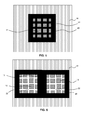
- FIG. 1 schematically depicts a top view
- FIG. 2 schematically depicts a cross section of an integrated sensor chip package according to an embodiment of the present invention.
- the integrated sensor chip package comprises a substrate 10, which may be any suitable substrate, e.g. a semiconductor substrate such as a silicon substrate, a silicon on insulator substrate, a silicon germanium substrate, and so on.
- the substrate 10 comprises a main surface having a region on which a plurality of photodetectors 12 is formed.
- 'formed on' is intended to at least include an embodiment in which the photodetectors 12 are formed on top of the main surface, an embodiment in which the photodetectors 12 are formed partially in the main surface and an embodiment in which the photodetectors 12 are formed embedded in the main surface 10a, i.e., sharing its photosensitive surface with the main surface of the substrate 10.
- the photodetectors 12 form part of a light sensor, which may comprise a plurality of groups of photodetectors for determining the intensity and directionality of the incident light.
- the light sensor may comprise a grid of photodetectors 12, in which rows and/or columns of the photodetectors 12 of the grid are arranged to cooperate in the detection of light.
- FIG. 1 and 2 schematically depict a 4x4 grid of photodetectors 12 by way of non-limiting example only. Any suitable grid size, e.g. comprising many more photodetectors 12 may be contemplated.
- the photodetectors 12 are laterally separated from each other by way of non-limiting example only. It is equally feasible that the areas of the respective photodetectors 12 contact each other. It should be understood that any suitable layout of the photodetectors 12 of the light sensor may be contemplated, e.g. regular or irregular grids, a central photodetector surrounded by peripheral photodetector and so on. It should also be understood that different photodetectors 12 may have different sizes, i.e. different size photosensitive areas. For instance, a light sensor may comprise a central photodetector 12 that is larger than the peripheral photodetectors 12.
- Each individual photodetector 12 on the main surface of the substrate 10 may have a photosensitive area of several tens of microns squared, e.g. 100 microns x 100 microns, to increase the sensitivity of the photodetector.
- the substrate or sensor chip 10 is typically packaged in a packaging layer 30 comprising an opening 32 to expose the photodetectors 12 on the substrate 10.
- Chip packaging is known per se and will not be explained in further detail for the sake of brevity. It should be understood that any suitable chip packaging material, e.g. a resin such as an epoxy resin, premolded packaging, a metal package such as a metal can and so on, may be used for the packaging layer 30.
- the opening 32 in the packaging layer 30 may be formed in any suitable manner, e.g. etching, laser cutting, stamping and the like.
- the opening 32 may be formed by pressing an insert into the packaging layer 30 during the molding process and removing the insert after curing of the packaging layer 30.
- the integrated sensor chip package further comprises at least one light blocking member 20 placed on the packaging layer 30.
- the light blocking member 20 is made of an opaque material such as a metal and is used to prevent exposure of some of the photodetectors 12a-d to incident light of certain angles of incidence, as is shown in FIG. 2 .
- the light blocking member 20 is a metal plate or a plate of another suitable opaque material.
- the light blocking member 20 defines an aperture 22 through which subsets of the photodetectors 12 may be exposed to incident light depending on the angle of incidence of the light.
- the aperture 22 has a square shape by way of non-limiting example only. It should be understood that the aperture 22 may have any suitable shape.
- the light blocking structure 20 at least partially overhangs or shades some of the photodetectors 12, such that only some of the photodetectors 12 are exposed to light at a certain angle of incidence.
- This is schematically depicted in FIG. 2 by the dashed lines indicating light passing through the aperture 22 under an angle ⁇ such that photodetectors 12a and 12c are only partially exposed to the incident light, whilst photodetector 12b is fully exposed and photodetector 12d is not exposed at all to incident light of angle ⁇ .
- the photodetector 12b when the integrated sensor chip package is exposed to light from a first direction, e.g. having an angle of incidence ⁇ , the photodetector 12b will produce a stronger photo-induced signal than the photodetectors 12a and 12c, and photodetector 12d will produce no more than a negligible signal, e.g. caused by incident scattered light.
- Different angles of incidence will expose a different subset of the photodetectors 12 to such incident light, such that each angle of incidence can be correlated to a unique signal combination in terms of signal intensity and originating photodetector 12.
- These signatures can be identified by a signal processor (not shown) to detect the orientation of the integrated sensor chip package relative to this angle of incidence.
- a signal processor may be provided on the integrated sensor chip or on a separate chip in the package.
- the intensity of the signals can furthermore be used to derive the intensity of the incident light as is well known per se.
- the light blocking member 20 is positioned on the finalized integrated sensor chip package, the light blocking member 20 can be accurately positioned relative to the photodetectors 12 as will be explained in more detail later. It is pointed out that this is an important advantage over prior art arrangements in which the light blocking members were integrated in the chip package as manufacturing tolerances in chip packaging of typically about 100 micron tend to prohibit accurate alignment of the light blocking member 20 with the region of the substrate 10 carrying the photodetectors 12. Such tolerances for instance cannot be avoided in cavity molding processes, in which the integrated sensor chip is moulded into the packaging layer 30 at elevated temperatures, which introduces a level of uncertainty about the precise position of the integrated sensor chip in the packaging layer 30.
- the light blocking member 20 may be affixed to the packaging layer 30 in any suitable manner.
- the light blocking member 20 is affixed to the packaging layer 30 using an adhesive, i.e. glue.
- FIG. 3 schematically depicts a cross section of another embodiment of an integrated sensor chip package according to the present invention.
- the integrated sensor chip package of FIG. 3 shares many elements of the integrated sensor chip package of FIG. 1 . Such shared features are identified using the same reference numerals and will not be explained in detail again for the sake of brevity.
- the surface of the packaging layer 30 in which the opening 32 is formed to expose the photodetectors 12 comprises a recessed surface portion 34, with the opening 32 being formed the said recessed surface portion 34.
- the surface of the packaging layer 30 in which the opening 32 is formed has a stepped profile.
- the light blocking member 20 is mounted on the recessed surface portion 34, e.g. by using an adhesive. This brings the light blocking member 20 in closer vicinity to the region of the substrate 10 carrying the photodetectors 12, which increases the viewing angle of the light directional sensor.
- this embodiment is particularly suitable for providing an integrated sensor chip package comprising a wide-angle light directional sensor.
- FIG. 4 schematically depicts a top view of an integrated sensor chip package comprising an opening 32 acting as a fluid channel for a fluid sensor 14 on the IC, e.g. on the main surface of the substrate 10, on top of the metallization stack of the integrated sensor chip and so on.
- the photodetectors 12 are also exposed by the opening 32 acting as a fluid channel.
- the light blocking member 20 is located over the opening 32 and may cooperate with the opening 32 to define the fluid channel.
- the aperture 22 partially exposes the photodetectors 12 as previously explained.
- the aperture 22 is a circular aperture in FIG. 4 by way of non-limiting example, simply to show that different shapes of apertures 22 may be used for the light blocking member 20.
- the light blocking member may comprise a single aperture 22 or multiple apertures 22 over a single region of photodetectors 12, as is shown in FIG. 5 .
- This embodiment can be used to provide a more fine-grained shading pattern over the photodetectors 12.
- the multiple apertures 22 may have any suitable shape, e.g. circular, oval, square, oblong shapes and so on.
- the sensor chip may comprise a substrate 10 comprising a plurality of light-sensitive regions, each region comprising a separate plurality of photodetectors 12, wherein the light blocking member 20 comprises multiple apertures 22 such that each aperture 22 provides shading to one of said light-sensitive regions. This is shown in FIG. 6 .
- the integrated sensor chip package according to embodiments of the present invention may be integrated in a suitable apparatus.
- the apparatus may be a Radio Frequency Identification (RFID) tag, a mobile communications device, examples of which include mobile telephones, tablets and laptops.
- RFID Radio Frequency Identification
- the apparatus alternatively may be a heating, ventilation and air conditioning (HVAC) system.
- the HVAC system can, for example, be provided in an automobile or in a building (e.g. a Smart Building).
- the apparatus may be a display device, in which case the light sensor of the integrated sensor chip may be used to provide information about the directionality of incident ambient light, which information may be used to adjust e.g. the brightness of (parts of) the image displayed on the display device to compensate for the incident light.
- Other applications can include use in the field of supply chain management to track and monitor the freshness of food and beverages. Additional applications include those in agricultural (e.g. the sensing of environmental conditions in greenhouses) or in medical fields.
- the integrated sensor chip package according to embodiments of the present invention may be manufactured in any suitable manner.
- the manufacturing of an integrated sensor chip comprising a plurality of photodetectors 12 and the packaging of such an integrated sensor chip in a packaging layer 30, e.g. through a cavity molding process is well-known per se such that this will not be explained in further detail for the sake of brevity only.
- FIG. 7 schematically depicts an aspect of such a manufacturing step in which the light blocking member 20 is aligned over the opening 32 in the packaging layer with the aid of optical tools, here a camera 50.
- the camera 50 is used to identify features on the part of the surface of the substrate 10 that is exposed through the aperture 22, such as the borders of the underlying photodetectors 12a-d, some markers of the substrate 10 or combinations thereof, and to provide feedback to a mechanical placement tool (not shown) responsible for the placement of the light blocking member 20 over the opening 32.
- This feedback mechanism can be used to accurately align the light blocking member 20 with the photodetectors 12a-d.
- FIG. 8 schematically depicts an alternative aspect of such a manufacturing step in which the light blocking member 20 is aligned over the opening 32 in the packaging layer with the aid of optical tools, here a light source 60.
- the photodetectors 12a-d are used to detect the light from the light source 60, such that the response from the photodetectors 12a-d is used as the feedback for the mechanical placement tool responsible for aligning the light blocking member 20 with the photodetectors 12a-d.
- the light blocking member 20 can be assumed to be in its intended position when the grid of photodetectors 12 produces a balanced or symmetrical output profile.
- This embodiment has the further benefit that the photodetectors 12a-d may be tested at the same time to detect malfunctioning photodetectors 12a-d.
- An adhesive may be present on the upper surface of the packaging layer 30, i.e. the surface receiving the light blocking member 20 and/or on the surface of the light blocking member 20 to be adhered to the packaging layer 30.
- This adhesive may be developed once the alignment of the light blocking member 20 relative to the photodetectors 12a-d has been completed, e.g. by drying or curing the adhesive.
Abstract
Description
- The present invention relates to an integrated sensor chip package comprising a substrate having a major surface; a light sensor, the light sensor comprising a plurality of photodetectors on a region of said major surface.
- The present invention further relates to a device including such an integrated sensor chip package.
- The present invention yet further relates to a method of manufacturing such an integrated sensor chip package.
- Nowadays, integrated sensors may comprise a plethora of different sensors, such as ambient light (AL) sensors, temperature (T) sensors, gas sensors, relative humidity (RH) sensors, integrated sensor chip analyte detection sensors, and so on.
- Integrated sensors of this kind have a wide range of applications. For example, they can be used in the field of supply chain management to track and monitor the freshness of food and beverages. They can also be used as environmental sensors, for example as part of a heating, ventilation and air conditioning (HVAC) system in an automobile or in a building (e.g. a Smart Building). Additional applications include those in agricultural (e.g. the sensing of environmental conditions in greenhouses) or in medical fields. Their provision in mobile communications devices such as mobile telephones, tablets or laptops can also enable a wide range of further applications that require measurements of local environmental factors.
- The provision of integrated sensor chips of this kind allows devices to be produced that have a small form factor, and which can be manufactured cheaply in large numbers using established semiconductor processing techniques.
- There is a constant desire to diversify the sensor functionality integrated into an integrated sensor chip to add further functionality to an apparatus utilizing the integrated sensor chip. For instance,
WO 2009/087531 by the present applicant discloses an integrated sensor chip having a light sensor that can detect both the intensity and direction of incident light, e.g. to compensate the output of a display device for ambient lighting conditions to improve the user experience of the display device. To this end, the light sensor comprises a dielectric layer, wherein the dielectric layer is substantially transparent to the incident light as well as a plurality of photo detectors coupled relative to the dielectric layer for detecting the incident light through the dielectric layer. A plurality of stacks of opaque slats embedded within the dielectric layer approximately parallel to an interface between the dielectric layer and the photo detectors is also present to define tapered light apertures between adjacent stacks of opaque slats. - Such a light sensor requires a relatively complex arrangement of tapered stacks of slats to make the light sensor directionally sensitive. There exists a need to simplify the design of such a light sensor.
- The present invention seeks to provide an integrated sensor chip package according to the opening paragraph in which sensitivity to the directionality of incident light is provided in a more straightforward manner.
- The present invention further seeks to provide an apparatus including such an integrated sensor chip package.
- The present invention yet further seeks to provide a method of manufacturing such an integrated sensor chip package.
- According to an aspect of the present invention, there is provided an integrated sensor chip package comprising an integrated sensor chip enveloped in a packaging layer, the integrated sensor chip comprising a substrate having a major surface; and a light sensor comprising a plurality of photodetectors on a region of said major surface; the packaging layer comprising an opening exposing said region, the integrated circuit package further comprising a light blocking member over said opening, the light blocking member defining an aperture exposing a first set of photodetectors to light from a first range of directions and exposing a second set of photodetectors to light from a second range of directions, wherein the first range is different to the second range.
- The present invention is based on the insight that a light shielding portion that shades different parts of the light sensor under different angles can be accurately positioned and fitted relative to the package of the integrated sensor chip , thereby providing a straightforward and cost-effective integrated sensor chip including a light sensor that can be used to detect directionality, e.g. the orientation of an apparatus including the integrated sensor chip package.
- In an embodiment, the light blocking member is a plate comprising said aperture. The plate may for instance be a metal plate made of any suitable metal such as aluminium. Such a light blocking member can be placed on the packaging layer in a straightforward manner, thus simplifying the manufacturing process.
- The light blocking member preferably is adhered to the packaging layer for ease of manufacture.
- In an embodiment, the packaging layer comprises a recessed surface portion, said opening being formed in said recessed surface portion, wherein the light blocking member is mounted on said recessed surface portion. This allows for the positioning of the light blocking member in close vicinity to the photodetectors, which allows for more effective angle-dependent shading of the photodetectors and a wide viewing angle of the light sensor.
- The integrated sensor chip may further comprise a fluid sensor such as a gas sensor, wherein the opening further may define a fluidic channel providing fluidic access to the fluid sensor. This obviates the need for a separate access channel to a fluid sensor such as a gas sensor, thereby simplifying the design of such a multi-sensor IC.
- In accordance with another aspect of the present invention, there is provided an apparatus comprising the integrated circuit package according to an embodiment of the present invention. Such an apparatus may for instance be one of a radio frequency identification tag; a mobile communications device; a display device; and a heating, ventilation and air-conditioning (HVAC) system, or any other device that can benefit from the inclusion of the integrated sensor chip package of the present invention.
- In accordance with yet another aspect of the present invention, there is provided a method of manufacturing an integrated sensor chip package, the method comprising providing an integrated sensor comprising a semiconductor substrate having a major surface; providing a light sensor in the integrated sensor chip by forming a plurality of photodetectors on a region of the major surface; packaging the integrated sensor chip in a packaging layer; creating an opening in the packaging layer to expose said region; and placing a light blocking member over said opening, the light blocking member defining an aperture exposing a first set of photodetectors to light from a first range of directions and exposing a second set of photodetectors to light from a second range of directions, wherein the first range is different to the second range. This method thus provides a simple and cost-effective manner of forming a light sensor in a packaged integrated sensor chip that can be used to determine the directionality of the incident light.
- The light blocking member may be fixed to the package layer in any suitable manner. In a particularly suitable embodiment, the step of placing said light blocking member over said opening comprises adhering the light blocking member to the packaging layer. This is a simple and cost-effective manner of fixing the light blocking member to the packaging layer.
- In an embodiment, the method further comprises the step of forming a recessed surface portion in said packaging layer and wherein the step of forming said opening comprises forming said opening in the recessed surface portion; and the step of placing a light blocking member over said opening comprises mounting said light blocking member on said recessed surface portion. This allows for the placement of the light blocking member in close vicinity to the photodetectors, which increases the width of the viewing angle of the light sensor.
- In an embodiment, the step of placing the light blocking member comprises optically aligning the light blocking member with said region. This ensures a highly accurate alignment of the light blocking member with the photodetectors, thus improving the accuracy of the light directional sensor.
- The optically aligning step may comprise aligning the light blocking member with said region using a camera or alternatively may comprise exposing at least some of said photodetectors to a light source through said aperture; measuring the response of the at least some of said photodetectors; and aligning the light blocking member with said region in accordance with said response. The latter embodiment has the further advantage that the testing of the photodetectors may be combined with the alignment of the light blocking member in a single step, thus obviating the need for separate testing of the photodetectors.
- Embodiments of the invention are described in more detail and by way of non-limiting examples with reference to the accompanying drawings, wherein:
-
FIG. 1 schematically depicts a top view of an integrated sensor chip package according to an embodiment of the present invention; -
FIG. 2 schematically depicts a cross section of an integrated sensor chip package according to an embodiment of the present invention; -
FIG. 3 schematically depicts a cross section of an integrated sensor chip package according to another embodiment of the present invention; -
FIG. 4 schematically depicts a top view of an integrated sensor chip package according to another embodiment of the present invention; -
FIG. 5 schematically depicts a top view of an integrated sensor chip package according to yet another embodiment of the present invention; -
FIG. 6 schematically depicts a top view of an integrated sensor chip package according to yet another embodiment of the present invention; -
FIG. 7 schematically depicts an aspect of an integrated sensor chip package manufacturing method according to an embodiment of the present invention; and -
FIG. 8 schematically depicts an aspect of an integrated sensor chip package manufacturing method according to another embodiment of the present invention. - It should be understood that the Figures are merely schematic and are not drawn to scale. It should also be understood that the same reference numerals are used throughout the Figures to indicate the same or similar parts.
-
FIG. 1 schematically depicts a top view andFIG. 2 schematically depicts a cross section of an integrated sensor chip package according to an embodiment of the present invention. The integrated sensor chip package comprises asubstrate 10, which may be any suitable substrate, e.g. a semiconductor substrate such as a silicon substrate, a silicon on insulator substrate, a silicon germanium substrate, and so on. Thesubstrate 10 comprises a main surface having a region on which a plurality ofphotodetectors 12 is formed. In the context of the present application, 'formed on' is intended to at least include an embodiment in which thephotodetectors 12 are formed on top of the main surface, an embodiment in which thephotodetectors 12 are formed partially in the main surface and an embodiment in which thephotodetectors 12 are formed embedded in the main surface 10a, i.e., sharing its photosensitive surface with the main surface of thesubstrate 10. - The
photodetectors 12 form part of a light sensor, which may comprise a plurality of groups of photodetectors for determining the intensity and directionality of the incident light. For instance, the light sensor may comprise a grid ofphotodetectors 12, in which rows and/or columns of thephotodetectors 12 of the grid are arranged to cooperate in the detection of light.FIG. 1 and 2 schematically depict a 4x4 grid ofphotodetectors 12 by way of non-limiting example only. Any suitable grid size, e.g. comprising manymore photodetectors 12 may be contemplated. - In
FIG. 1 and 2 , thephotodetectors 12 are laterally separated from each other by way of non-limiting example only. It is equally feasible that the areas of therespective photodetectors 12 contact each other. It should be understood that any suitable layout of thephotodetectors 12 of the light sensor may be contemplated, e.g. regular or irregular grids, a central photodetector surrounded by peripheral photodetector and so on. It should also be understood thatdifferent photodetectors 12 may have different sizes, i.e. different size photosensitive areas. For instance, a light sensor may comprise acentral photodetector 12 that is larger than theperipheral photodetectors 12. Eachindividual photodetector 12 on the main surface of thesubstrate 10 may have a photosensitive area of several tens of microns squared, e.g. 100 microns x 100 microns, to increase the sensitivity of the photodetector. - The substrate or
sensor chip 10 is typically packaged in apackaging layer 30 comprising anopening 32 to expose thephotodetectors 12 on thesubstrate 10. Chip packaging is known per se and will not be explained in further detail for the sake of brevity. It should be understood that any suitable chip packaging material, e.g. a resin such as an epoxy resin, premolded packaging, a metal package such as a metal can and so on, may be used for thepackaging layer 30. Theopening 32 in thepackaging layer 30 may be formed in any suitable manner, e.g. etching, laser cutting, stamping and the like. Alternatively, in case of thepackaging layer 30 comprising a resin, theopening 32 may be formed by pressing an insert into thepackaging layer 30 during the molding process and removing the insert after curing of thepackaging layer 30. - The integrated sensor chip package according to embodiments of the present invention further comprises at least one
light blocking member 20 placed on thepackaging layer 30. Thelight blocking member 20 is made of an opaque material such as a metal and is used to prevent exposure of some of thephotodetectors 12a-d to incident light of certain angles of incidence, as is shown inFIG. 2 . In an embodiment, thelight blocking member 20 is a metal plate or a plate of another suitable opaque material. Thelight blocking member 20 defines anaperture 22 through which subsets of thephotodetectors 12 may be exposed to incident light depending on the angle of incidence of the light. InFIG. 1 , theaperture 22 has a square shape by way of non-limiting example only. It should be understood that theaperture 22 may have any suitable shape. - As can be seen in
FIG. 1 and 2 , thelight blocking structure 20 at least partially overhangs or shades some of thephotodetectors 12, such that only some of thephotodetectors 12 are exposed to light at a certain angle of incidence. This is schematically depicted inFIG. 2 by the dashed lines indicating light passing through theaperture 22 under an angle α such thatphotodetectors photodetector 12b is fully exposed andphotodetector 12d is not exposed at all to incident light of angle α. - Consequently, when the integrated sensor chip package is exposed to light from a first direction, e.g. having an angle of incidence α, the
photodetector 12b will produce a stronger photo-induced signal than thephotodetectors photodetector 12d will produce no more than a negligible signal, e.g. caused by incident scattered light. Different angles of incidence will expose a different subset of thephotodetectors 12 to such incident light, such that each angle of incidence can be correlated to a unique signal combination in terms of signal intensity and originatingphotodetector 12. These signatures can be identified by a signal processor (not shown) to detect the orientation of the integrated sensor chip package relative to this angle of incidence. Such a signal processor may be provided on the integrated sensor chip or on a separate chip in the package. The intensity of the signals can furthermore be used to derive the intensity of the incident light as is well known per se. - Because the
light blocking member 20 is positioned on the finalized integrated sensor chip package, thelight blocking member 20 can be accurately positioned relative to thephotodetectors 12 as will be explained in more detail later. It is pointed out that this is an important advantage over prior art arrangements in which the light blocking members were integrated in the chip package as manufacturing tolerances in chip packaging of typically about 100 micron tend to prohibit accurate alignment of thelight blocking member 20 with the region of thesubstrate 10 carrying thephotodetectors 12. Such tolerances for instance cannot be avoided in cavity molding processes, in which the integrated sensor chip is moulded into thepackaging layer 30 at elevated temperatures, which introduces a level of uncertainty about the precise position of the integrated sensor chip in thepackaging layer 30. - The
light blocking member 20 may be affixed to thepackaging layer 30 in any suitable manner. In an embodiment, thelight blocking member 20 is affixed to thepackaging layer 30 using an adhesive, i.e. glue. -
FIG. 3 schematically depicts a cross section of another embodiment of an integrated sensor chip package according to the present invention. The integrated sensor chip package ofFIG. 3 shares many elements of the integrated sensor chip package ofFIG. 1 . Such shared features are identified using the same reference numerals and will not be explained in detail again for the sake of brevity. InFIG. 3 , the surface of thepackaging layer 30 in which theopening 32 is formed to expose thephotodetectors 12 comprises a recessedsurface portion 34, with theopening 32 being formed the said recessedsurface portion 34. In other words, the surface of thepackaging layer 30 in which theopening 32 is formed has a stepped profile. Thelight blocking member 20 is mounted on the recessedsurface portion 34, e.g. by using an adhesive. This brings thelight blocking member 20 in closer vicinity to the region of thesubstrate 10 carrying thephotodetectors 12, which increases the viewing angle of the light directional sensor. Hence, this embodiment is particularly suitable for providing an integrated sensor chip package comprising a wide-angle light directional sensor. - As previously explained, ICs can contain a wide variety of sensors. A particularly interesting class of sensors is fluid sensors, e.g. gas or moisture sensors, relative humidity sensors, and so on. Such sensors must be exposed to the environment of the integrated sensor chip package, i.e. the integrated sensor chip package must contain an opening to expose such a fluid sensor to its environment.
FIG. 4 schematically depicts a top view of an integrated sensor chip package comprising anopening 32 acting as a fluid channel for afluid sensor 14 on the IC, e.g. on the main surface of thesubstrate 10, on top of the metallization stack of the integrated sensor chip and so on. - The
photodetectors 12 are also exposed by theopening 32 acting as a fluid channel. Thelight blocking member 20 is located over theopening 32 and may cooperate with theopening 32 to define the fluid channel. Theaperture 22 partially exposes thephotodetectors 12 as previously explained. Theaperture 22 is a circular aperture inFIG. 4 by way of non-limiting example, simply to show that different shapes ofapertures 22 may be used for thelight blocking member 20. - It is noted at this point that the light blocking member may comprise a
single aperture 22 ormultiple apertures 22 over a single region ofphotodetectors 12, as is shown inFIG. 5 . This embodiment can be used to provide a more fine-grained shading pattern over thephotodetectors 12. Themultiple apertures 22 may have any suitable shape, e.g. circular, oval, square, oblong shapes and so on. Alternatively, the sensor chip may comprise asubstrate 10 comprising a plurality of light-sensitive regions, each region comprising a separate plurality ofphotodetectors 12, wherein thelight blocking member 20 comprisesmultiple apertures 22 such that eachaperture 22 provides shading to one of said light-sensitive regions. This is shown inFIG. 6 . - The integrated sensor chip package according to embodiments of the present invention may be integrated in a suitable apparatus. For example, the apparatus may be a Radio Frequency Identification (RFID) tag, a mobile communications device, examples of which include mobile telephones, tablets and laptops. The apparatus alternatively may be a heating, ventilation and air conditioning (HVAC) system. The HVAC system can, for example, be provided in an automobile or in a building (e.g. a Smart Building).
- The apparatus may be a display device, in which case the light sensor of the integrated sensor chip may be used to provide information about the directionality of incident ambient light, which information may be used to adjust e.g. the brightness of (parts of) the image displayed on the display device to compensate for the incident light. Other applications can include use in the field of supply chain management to track and monitor the freshness of food and beverages. Additional applications include those in agricultural (e.g. the sensing of environmental conditions in greenhouses) or in medical fields.
- The integrated sensor chip package according to embodiments of the present invention may be manufactured in any suitable manner. In particular, the manufacturing of an integrated sensor chip comprising a plurality of
photodetectors 12 and the packaging of such an integrated sensor chip in apackaging layer 30, e.g. through a cavity molding process, is well-known per se such that this will not be explained in further detail for the sake of brevity only. -
FIG. 7 schematically depicts an aspect of such a manufacturing step in which thelight blocking member 20 is aligned over theopening 32 in the packaging layer with the aid of optical tools, here acamera 50. Thecamera 50 is used to identify features on the part of the surface of thesubstrate 10 that is exposed through theaperture 22, such as the borders of theunderlying photodetectors 12a-d, some markers of thesubstrate 10 or combinations thereof, and to provide feedback to a mechanical placement tool (not shown) responsible for the placement of thelight blocking member 20 over theopening 32. This feedback mechanism can be used to accurately align thelight blocking member 20 with thephotodetectors 12a-d. -
FIG. 8 schematically depicts an alternative aspect of such a manufacturing step in which thelight blocking member 20 is aligned over theopening 32 in the packaging layer with the aid of optical tools, here alight source 60. In this embodiment, thephotodetectors 12a-d are used to detect the light from thelight source 60, such that the response from thephotodetectors 12a-d is used as the feedback for the mechanical placement tool responsible for aligning thelight blocking member 20 with thephotodetectors 12a-d. For instance, thelight blocking member 20 can be assumed to be in its intended position when the grid ofphotodetectors 12 produces a balanced or symmetrical output profile. This embodiment has the further benefit that thephotodetectors 12a-d may be tested at the same time to detect malfunctioningphotodetectors 12a-d. - An adhesive may be present on the upper surface of the
packaging layer 30, i.e. the surface receiving thelight blocking member 20 and/or on the surface of thelight blocking member 20 to be adhered to thepackaging layer 30. This adhesive may be developed once the alignment of thelight blocking member 20 relative to thephotodetectors 12a-d has been completed, e.g. by drying or curing the adhesive. - It should be noted that the above-mentioned embodiments illustrate rather than limit the invention, and that those skilled in the art will be able to design many alternative embodiments without departing from the scope of the appended claims. In the claims, any reference signs placed between parentheses shall not be construed as limiting the claim. The word "comprising" does not exclude the presence of elements or steps other than those listed in a claim. The word "a" or "an" preceding an element does not exclude the presence of a plurality of such elements. The invention can be implemented by means of hardware comprising several distinct elements. In the device claim enumerating several means, several of these means can be embodied by one and the same item of hardware. The mere fact that certain measures are recited in mutually different dependent claims does not indicate that a combination of these measures cannot be used to advantage.
Claims (15)
- An integrated sensor chip package comprising an integrated circuit enveloped in a packaging layer (30), the integrated sensor chip comprising:a substrate (10) having a major surface; anda light sensor comprising a plurality of photodetectors (12a-d) on a region of said major surface;the packaging layer comprising an opening (32) exposing said region, the integrated circuit package further comprising a light blocking member (20) over said opening, the light blocking member defining an aperture (22) exposing a first set of photodetectors to light from a first range of directions and exposing a second set of photodetectors to light from a second range of directions, wherein the first range is different to the second range.
- The integrated sensor chip package of claim 1, wherein the light blocking member (20) is a plate comprising said aperture (22).
- The integrated sensor chip package of claim 2, wherein the plate is a metal plate.
- The integrated sensor chip package of any of claims 1-3, wherein the light blocking member (20) is adhered to the packaging layer (30).
- The integrated sensor chip package of any of claims 1-4, wherein the packaging layer (30) comprises a recessed surface portion (34), said opening (32) being formed in said recessed surface portion, wherein the light blocking member (20) is mounted on said recessed surface portion.
- The integrated sensor chip package of any of claims 1-4, wherein the integrated circuit further comprises a fluid sensor (14), wherein the opening (32) cooperates with the light blocking member (20) to define a fluidic channel providing fluidic access to the fluid sensor.
- An apparatus comprising the integrated sensor chip package of any of claims 1-6.
- The apparatus of claim 7, wherein the apparatus is one of:a radio frequency identification tag;a mobile communications device;a display device; anda heating, ventilation and air-conditioning (HVAC) system.
- A method of manufacturing an integrated sensor chip package, the method comprising:providing an integrated sensor chip comprising a semiconductor substrate (10) having a major surface;providing a light sensor in the integrated sensor chip by forming a plurality of photodetectors (12a-d) on a region of the major surface;packaging the integrated sensor chip in a packaging layer (30);creating an opening (32) in the packaging layer to expose said region; andplacing a light blocking member (20) over said opening, the light blocking member defining an aperture (22) exposing a first set of photodetectors to light from a first range of directions and exposing a second set of photodetectors to light from a second range of directions , wherein the first range is different to the second range.
- The method of claim 9, wherein the step of placing said light blocking member (20) over said opening (32) comprises adhering the light blocking member to the packaging layer (30).
- The method of claim 9 or 10, wherein the light blocking member (20) is a plate comprising said aperture (22).
- The method of any of claims 9-11, further comprising the step of forming a recessed surface portion (34) in said packaging layer (30) and wherein:the step of forming said opening (32) comprises forming said opening in the recessed surface portion; andthe step of placing a light blocking member (20) over said opening comprises mounting said light blocking member on said recessed surface portion.
- The method of any of claims 8-12, wherein the step of placing the light blocking member (20) comprises optically aligning the light blocking member with said region.
- The method of claim 13, wherein said optically aligning step comprises aligning the light blocking member (20) with said region using a camera (50).
- The method of claim 13, wherein said optically aligning step comprises:exposing at least some of said photodetectors (12) to a light source (60) through said aperture;measuring the response of the at least some of said photodetectors; andaligning the light blocking member (20) with said region in accordance with said response.
Priority Applications (2)
| Application Number | Priority Date | Filing Date | Title |
|---|---|---|---|
| EP13171297.8A EP2814064B1 (en) | 2013-06-10 | 2013-06-10 | Integrated sensor chip package with directional light sensor, apparatus including such a package and method of manufacturing such an integrated sensor chip package |
| US14/299,560 US9666637B2 (en) | 2013-06-10 | 2014-06-09 | Integrated sensor chip package with directional light sensor, apparatus including such a package and method of manufacturing such an integrated sensor chip package |
Applications Claiming Priority (1)
| Application Number | Priority Date | Filing Date | Title |
|---|---|---|---|
| EP13171297.8A EP2814064B1 (en) | 2013-06-10 | 2013-06-10 | Integrated sensor chip package with directional light sensor, apparatus including such a package and method of manufacturing such an integrated sensor chip package |
Publications (2)
| Publication Number | Publication Date |
|---|---|
| EP2814064A1 true EP2814064A1 (en) | 2014-12-17 |
| EP2814064B1 EP2814064B1 (en) | 2020-11-25 |
Family
ID=48576890
Family Applications (1)
| Application Number | Title | Priority Date | Filing Date |
|---|---|---|---|
| EP13171297.8A Active EP2814064B1 (en) | 2013-06-10 | 2013-06-10 | Integrated sensor chip package with directional light sensor, apparatus including such a package and method of manufacturing such an integrated sensor chip package |
Country Status (2)
| Country | Link |
|---|---|
| US (1) | US9666637B2 (en) |
| EP (1) | EP2814064B1 (en) |
Families Citing this family (2)
| Publication number | Priority date | Publication date | Assignee | Title |
|---|---|---|---|---|
| FR3045792B1 (en) * | 2015-12-21 | 2018-04-06 | Commissariat A L'energie Atomique Et Aux Energies Alternatives | DEVICE FOR MEASURING FLOWS REFLECTED BY A SOLAR FIELD PROVIDED WITH A SYSTEM WITH VARIABLE CONFIGURATION IN RELATION TO PHOTODETECTORS OF SAID MEASURING DEVICE |
| CN108709905B (en) * | 2018-06-25 | 2020-10-30 | 复旦大学 | Light enhancement type gas sensitive element based on non-uniform illumination |
Citations (7)
| Publication number | Priority date | Publication date | Assignee | Title |
|---|---|---|---|---|
| FR2601443A1 (en) * | 1986-07-10 | 1988-01-15 | Centre Nat Etd Spatiales | Position sensor and its application in telemetry, in particular space robotics |
| CA2119330A1 (en) * | 1994-03-17 | 1995-09-18 | Ishiang Shih | Methods to determine spatial angle of a light beam |
| EP1189072A2 (en) * | 2000-09-19 | 2002-03-20 | Jena-Optronik GmbH | Device for determining the angle of incidence of light |
| US20050237415A1 (en) * | 2004-04-26 | 2005-10-27 | Yung-Cheol Kong | Image sensor module having auto-aligned lens, and method of fabricating the same, and method of automatically controlling focus of lens |
| WO2009087531A1 (en) | 2008-01-02 | 2009-07-16 | Nxp B.V. | Light sensor with intensity and direction detection |
| WO2011058190A1 (en) * | 2009-11-16 | 2011-05-19 | Opto-Mst Sensoren Und Systeme Gmbh | Device and method for localizing modulated optical radiation sources |
| US20110170105A1 (en) * | 2008-03-04 | 2011-07-14 | Xiquan Cui | Techniques for Improving Optofluidic Microscope Devices |
Family Cites Families (20)
| Publication number | Priority date | Publication date | Assignee | Title |
|---|---|---|---|---|
| JPS5624969A (en) * | 1979-08-09 | 1981-03-10 | Canon Inc | Semiconductor integrated circuit element |
| JPH01164073A (en) * | 1987-09-11 | 1989-06-28 | Canon Inc | Optoelectric conversion device |
| US5264691A (en) * | 1991-07-26 | 1993-11-23 | Hegyi Dennis J | System for determining the direction of incident optical radiation |
| US5534725A (en) * | 1992-06-16 | 1996-07-09 | Goldstar Electron Co., Ltd. | Resin molded charge coupled device package and method for preparation thereof |
| JPH06117924A (en) * | 1992-08-19 | 1994-04-28 | Nippondenso Co Ltd | Optical position detector |
| KR960009089B1 (en) * | 1993-03-04 | 1996-07-10 | 문정환 | Mold for package molding and plastic charge-coupled device and the manufacturing method using the mold |
| US5553661A (en) * | 1995-10-23 | 1996-09-10 | Delco Electronics Corporation | Solar position correction for climate control system |
| US6075237A (en) * | 1998-07-29 | 2000-06-13 | Eastman Kodak Company | Image sensor cover with integral light shield |
| JP2002156280A (en) * | 2000-08-15 | 2002-05-31 | Nikon Corp | Luminous intensity measuring apparatus, exposure device and exposure method |
| JP3955487B2 (en) * | 2002-03-19 | 2007-08-08 | 松下電器産業株式会社 | Method for mounting integrated circuit element |
| DE10218160C1 (en) * | 2002-04-23 | 2003-12-24 | Elmos Semiconductor Ag | Device for determining the angle of incidence of radiation on a radiation incidence surface |
| US7535071B2 (en) * | 2004-03-29 | 2009-05-19 | Evolution Robotics, Inc. | System and method of integrating optics into an IC package |
| US7145253B1 (en) * | 2004-06-09 | 2006-12-05 | Amkor Technology, Inc. | Encapsulated sensor device |
| TWI297920B (en) * | 2006-02-22 | 2008-06-11 | Advanced Semiconductor Eng | Compact camera module and its substrate |
| US20090134481A1 (en) * | 2007-11-28 | 2009-05-28 | Analog Devices, Inc. | Molded Sensor Package and Assembly Method |
| US8629389B2 (en) * | 2009-07-29 | 2014-01-14 | Geoffrey Louis Barrows | Low profile camera and vision sensor |
| US8384559B2 (en) * | 2010-04-13 | 2013-02-26 | Silicon Laboratories Inc. | Sensor device with flexible interface and updatable information store |
| JP5930263B2 (en) * | 2011-02-18 | 2016-06-08 | ソニー株式会社 | Solid-state imaging device |
| US9702690B2 (en) * | 2011-12-19 | 2017-07-11 | Analog Devices, Inc. | Lens-less optical position measuring sensor |
| EP2662895B1 (en) | 2012-05-11 | 2014-06-25 | Nxp B.V. | Integrated circuit including a directional light sensor |
-
2013
- 2013-06-10 EP EP13171297.8A patent/EP2814064B1/en active Active
-
2014
- 2014-06-09 US US14/299,560 patent/US9666637B2/en active Active
Patent Citations (7)
| Publication number | Priority date | Publication date | Assignee | Title |
|---|---|---|---|---|
| FR2601443A1 (en) * | 1986-07-10 | 1988-01-15 | Centre Nat Etd Spatiales | Position sensor and its application in telemetry, in particular space robotics |
| CA2119330A1 (en) * | 1994-03-17 | 1995-09-18 | Ishiang Shih | Methods to determine spatial angle of a light beam |
| EP1189072A2 (en) * | 2000-09-19 | 2002-03-20 | Jena-Optronik GmbH | Device for determining the angle of incidence of light |
| US20050237415A1 (en) * | 2004-04-26 | 2005-10-27 | Yung-Cheol Kong | Image sensor module having auto-aligned lens, and method of fabricating the same, and method of automatically controlling focus of lens |
| WO2009087531A1 (en) | 2008-01-02 | 2009-07-16 | Nxp B.V. | Light sensor with intensity and direction detection |
| US20110170105A1 (en) * | 2008-03-04 | 2011-07-14 | Xiquan Cui | Techniques for Improving Optofluidic Microscope Devices |
| WO2011058190A1 (en) * | 2009-11-16 | 2011-05-19 | Opto-Mst Sensoren Und Systeme Gmbh | Device and method for localizing modulated optical radiation sources |
Also Published As
| Publication number | Publication date |
|---|---|
| EP2814064B1 (en) | 2020-11-25 |
| US9666637B2 (en) | 2017-05-30 |
| US20140361394A1 (en) | 2014-12-11 |
Similar Documents
| Publication | Publication Date | Title |
|---|---|---|
| CN108511538B (en) | Optoelectronic module | |
| US20210151511A1 (en) | Display device having fingerprint recognition sensor coupled thereto | |
| CN101542246A (en) | Spectroscopic module | |
| US9702690B2 (en) | Lens-less optical position measuring sensor | |
| JP6294500B2 (en) | Light emitting / receiving element module and sensor device using the same | |
| CN104247020A (en) | Reflowable opto-electronic module | |
| EP2339632A1 (en) | Image sensor and method of manufacturing the same, and sensor device | |
| WO2018223810A1 (en) | Biosensor, and preparation and biosensing method therefor | |
| EP2847797B1 (en) | Integrated circuit with directional light sensor, device including such an ic | |
| TWI320213B (en) | ||
| US9666637B2 (en) | Integrated sensor chip package with directional light sensor, apparatus including such a package and method of manufacturing such an integrated sensor chip package | |
| KR100555517B1 (en) | Method for measuring stray light and measuring system therefor | |
| WO2020228816A1 (en) | Microfluidic chip, detection method therefor, and micro total analysis system | |
| JP2010105153A (en) | Mems device and method for assembling microelectromechanical system (mems) | |
| CN101689541A (en) | Integrated circuits on a wafer and methods for manufacturing integrated circuits | |
| CN104115288B (en) | There is the infrared light transducer[sensor chip of high measurement accuracy and for the method manufacturing infrared light transducer[sensor chip | |
| US20240019377A1 (en) | Test strip cassette, monitoring device and method for fabricating a test strip cassette | |
| CN109283510A (en) | Light sensing apparatus and electronic equipment | |
| KR20190023622A (en) | Omnidirectional image sensor and manufacturing method thereof | |
| CN109904245B (en) | Light-transmitting microporous structure for small-spacing infrared detector crosstalk test and preparation method thereof | |
| CN102136438B (en) | Method for quickly detecting segment difference height between stacked frames of chip | |
| EP2834846B1 (en) | Immunoassay device with photovoltaic sensor array | |
| KR20190019880A (en) | Display having integrated fingerprint sensor | |
| JP2012058084A (en) | Method of manufacturing infrared sensor device, and the infrared sensor device manufactured by the method | |
| KR20170019623A (en) | Position sensitive photo detector and method of manufacturing the same |
Legal Events
| Date | Code | Title | Description |
|---|---|---|---|
| 17P | Request for examination filed |
Effective date: 20140326 |
|
| AK | Designated contracting states |
Kind code of ref document: A1 Designated state(s): AL AT BE BG CH CY CZ DE DK EE ES FI FR GB GR HR HU IE IS IT LI LT LU LV MC MK MT NL NO PL PT RO RS SE SI SK SM TR |
|
| AX | Request for extension of the european patent |
Extension state: BA ME |
|
| PUAI | Public reference made under article 153(3) epc to a published international application that has entered the european phase |
Free format text: ORIGINAL CODE: 0009012 |
|
| RBV | Designated contracting states (corrected) |
Designated state(s): AL AT BE BG CH CY CZ DE DK EE ES FI FR GB GR HR HU IE IS IT LI LT LU LV MC MK MT NL NO PL PT RO RS SE SI SK SM TR |
|
| STAA | Information on the status of an ep patent application or granted ep patent |
Free format text: STATUS: EXAMINATION IS IN PROGRESS |
|
| 17Q | First examination report despatched |
Effective date: 20180907 |
|
| GRAP | Despatch of communication of intention to grant a patent |
Free format text: ORIGINAL CODE: EPIDOSNIGR1 |
|
| STAA | Information on the status of an ep patent application or granted ep patent |
Free format text: STATUS: GRANT OF PATENT IS INTENDED |
|
| INTG | Intention to grant announced |
Effective date: 20200720 |
|
| GRAS | Grant fee paid |
Free format text: ORIGINAL CODE: EPIDOSNIGR3 |
|
| GRAA | (expected) grant |
Free format text: ORIGINAL CODE: 0009210 |
|
| STAA | Information on the status of an ep patent application or granted ep patent |
Free format text: STATUS: THE PATENT HAS BEEN GRANTED |
|
| AK | Designated contracting states |
Kind code of ref document: B1 Designated state(s): AL AT BE BG CH CY CZ DE DK EE ES FI FR GB GR HR HU IE IS IT LI LT LU LV MC MK MT NL NO PL PT RO RS SE SI SK SM TR |
|
| REG | Reference to a national code |
Ref country code: GB Ref legal event code: FG4D |
|
| REG | Reference to a national code |
Ref country code: CH Ref legal event code: EP |
|
| REG | Reference to a national code |
Ref country code: AT Ref legal event code: REF Ref document number: 1339275 Country of ref document: AT Kind code of ref document: T Effective date: 20201215 |
|
| REG | Reference to a national code |
Ref country code: DE Ref legal event code: R096 Ref document number: 602013074249 Country of ref document: DE |
|
| REG | Reference to a national code |
Ref country code: IE Ref legal event code: FG4D |
|
| REG | Reference to a national code |
Ref country code: AT Ref legal event code: MK05 Ref document number: 1339275 Country of ref document: AT Kind code of ref document: T Effective date: 20201125 |
|
| REG | Reference to a national code |
Ref country code: NL Ref legal event code: MP Effective date: 20201125 |
|
| PG25 | Lapsed in a contracting state [announced via postgrant information from national office to epo] |
Ref country code: GR Free format text: LAPSE BECAUSE OF FAILURE TO SUBMIT A TRANSLATION OF THE DESCRIPTION OR TO PAY THE FEE WITHIN THE PRESCRIBED TIME-LIMIT Effective date: 20210226 Ref country code: FI Free format text: LAPSE BECAUSE OF FAILURE TO SUBMIT A TRANSLATION OF THE DESCRIPTION OR TO PAY THE FEE WITHIN THE PRESCRIBED TIME-LIMIT Effective date: 20201125 Ref country code: RS Free format text: LAPSE BECAUSE OF FAILURE TO SUBMIT A TRANSLATION OF THE DESCRIPTION OR TO PAY THE FEE WITHIN THE PRESCRIBED TIME-LIMIT Effective date: 20201125 Ref country code: PT Free format text: LAPSE BECAUSE OF FAILURE TO SUBMIT A TRANSLATION OF THE DESCRIPTION OR TO PAY THE FEE WITHIN THE PRESCRIBED TIME-LIMIT Effective date: 20210325 Ref country code: NO Free format text: LAPSE BECAUSE OF FAILURE TO SUBMIT A TRANSLATION OF THE DESCRIPTION OR TO PAY THE FEE WITHIN THE PRESCRIBED TIME-LIMIT Effective date: 20210225 |
|
| PG25 | Lapsed in a contracting state [announced via postgrant information from national office to epo] |
Ref country code: AT Free format text: LAPSE BECAUSE OF FAILURE TO SUBMIT A TRANSLATION OF THE DESCRIPTION OR TO PAY THE FEE WITHIN THE PRESCRIBED TIME-LIMIT Effective date: 20201125 Ref country code: BG Free format text: LAPSE BECAUSE OF FAILURE TO SUBMIT A TRANSLATION OF THE DESCRIPTION OR TO PAY THE FEE WITHIN THE PRESCRIBED TIME-LIMIT Effective date: 20210225 Ref country code: IS Free format text: LAPSE BECAUSE OF FAILURE TO SUBMIT A TRANSLATION OF THE DESCRIPTION OR TO PAY THE FEE WITHIN THE PRESCRIBED TIME-LIMIT Effective date: 20210325 Ref country code: SE Free format text: LAPSE BECAUSE OF FAILURE TO SUBMIT A TRANSLATION OF THE DESCRIPTION OR TO PAY THE FEE WITHIN THE PRESCRIBED TIME-LIMIT Effective date: 20201125 Ref country code: LV Free format text: LAPSE BECAUSE OF FAILURE TO SUBMIT A TRANSLATION OF THE DESCRIPTION OR TO PAY THE FEE WITHIN THE PRESCRIBED TIME-LIMIT Effective date: 20201125 Ref country code: PL Free format text: LAPSE BECAUSE OF FAILURE TO SUBMIT A TRANSLATION OF THE DESCRIPTION OR TO PAY THE FEE WITHIN THE PRESCRIBED TIME-LIMIT Effective date: 20201125 |
|
| REG | Reference to a national code |
Ref country code: LT Ref legal event code: MG9D |
|
| PG25 | Lapsed in a contracting state [announced via postgrant information from national office to epo] |
Ref country code: HR Free format text: LAPSE BECAUSE OF FAILURE TO SUBMIT A TRANSLATION OF THE DESCRIPTION OR TO PAY THE FEE WITHIN THE PRESCRIBED TIME-LIMIT Effective date: 20201125 |
|
| PG25 | Lapsed in a contracting state [announced via postgrant information from national office to epo] |
Ref country code: SM Free format text: LAPSE BECAUSE OF FAILURE TO SUBMIT A TRANSLATION OF THE DESCRIPTION OR TO PAY THE FEE WITHIN THE PRESCRIBED TIME-LIMIT Effective date: 20201125 Ref country code: CZ Free format text: LAPSE BECAUSE OF FAILURE TO SUBMIT A TRANSLATION OF THE DESCRIPTION OR TO PAY THE FEE WITHIN THE PRESCRIBED TIME-LIMIT Effective date: 20201125 Ref country code: EE Free format text: LAPSE BECAUSE OF FAILURE TO SUBMIT A TRANSLATION OF THE DESCRIPTION OR TO PAY THE FEE WITHIN THE PRESCRIBED TIME-LIMIT Effective date: 20201125 Ref country code: LT Free format text: LAPSE BECAUSE OF FAILURE TO SUBMIT A TRANSLATION OF THE DESCRIPTION OR TO PAY THE FEE WITHIN THE PRESCRIBED TIME-LIMIT Effective date: 20201125 Ref country code: SK Free format text: LAPSE BECAUSE OF FAILURE TO SUBMIT A TRANSLATION OF THE DESCRIPTION OR TO PAY THE FEE WITHIN THE PRESCRIBED TIME-LIMIT Effective date: 20201125 Ref country code: RO Free format text: LAPSE BECAUSE OF FAILURE TO SUBMIT A TRANSLATION OF THE DESCRIPTION OR TO PAY THE FEE WITHIN THE PRESCRIBED TIME-LIMIT Effective date: 20201125 |
|
| REG | Reference to a national code |
Ref country code: DE Ref legal event code: R097 Ref document number: 602013074249 Country of ref document: DE |
|
| PG25 | Lapsed in a contracting state [announced via postgrant information from national office to epo] |
Ref country code: DK Free format text: LAPSE BECAUSE OF FAILURE TO SUBMIT A TRANSLATION OF THE DESCRIPTION OR TO PAY THE FEE WITHIN THE PRESCRIBED TIME-LIMIT Effective date: 20201125 |
|
| PLBE | No opposition filed within time limit |
Free format text: ORIGINAL CODE: 0009261 |
|
| STAA | Information on the status of an ep patent application or granted ep patent |
Free format text: STATUS: NO OPPOSITION FILED WITHIN TIME LIMIT |
|
| PG25 | Lapsed in a contracting state [announced via postgrant information from national office to epo] |
Ref country code: IT Free format text: LAPSE BECAUSE OF FAILURE TO SUBMIT A TRANSLATION OF THE DESCRIPTION OR TO PAY THE FEE WITHIN THE PRESCRIBED TIME-LIMIT Effective date: 20201125 Ref country code: AL Free format text: LAPSE BECAUSE OF FAILURE TO SUBMIT A TRANSLATION OF THE DESCRIPTION OR TO PAY THE FEE WITHIN THE PRESCRIBED TIME-LIMIT Effective date: 20201125 Ref country code: NL Free format text: LAPSE BECAUSE OF FAILURE TO SUBMIT A TRANSLATION OF THE DESCRIPTION OR TO PAY THE FEE WITHIN THE PRESCRIBED TIME-LIMIT Effective date: 20201125 |
|
| 26N | No opposition filed |
Effective date: 20210826 |
|
| PG25 | Lapsed in a contracting state [announced via postgrant information from national office to epo] |
Ref country code: ES Free format text: LAPSE BECAUSE OF FAILURE TO SUBMIT A TRANSLATION OF THE DESCRIPTION OR TO PAY THE FEE WITHIN THE PRESCRIBED TIME-LIMIT Effective date: 20201125 Ref country code: SI Free format text: LAPSE BECAUSE OF FAILURE TO SUBMIT A TRANSLATION OF THE DESCRIPTION OR TO PAY THE FEE WITHIN THE PRESCRIBED TIME-LIMIT Effective date: 20201125 |
|
| PG25 | Lapsed in a contracting state [announced via postgrant information from national office to epo] |
Ref country code: MC Free format text: LAPSE BECAUSE OF FAILURE TO SUBMIT A TRANSLATION OF THE DESCRIPTION OR TO PAY THE FEE WITHIN THE PRESCRIBED TIME-LIMIT Effective date: 20201125 |
|
| REG | Reference to a national code |
Ref country code: CH Ref legal event code: PL |
|
| GBPC | Gb: european patent ceased through non-payment of renewal fee |
Effective date: 20210610 |
|
| REG | Reference to a national code |
Ref country code: BE Ref legal event code: MM Effective date: 20210630 |
|
| PG25 | Lapsed in a contracting state [announced via postgrant information from national office to epo] |
Ref country code: LU Free format text: LAPSE BECAUSE OF NON-PAYMENT OF DUE FEES Effective date: 20210610 |
|
| PG25 | Lapsed in a contracting state [announced via postgrant information from national office to epo] |
Ref country code: LI Free format text: LAPSE BECAUSE OF NON-PAYMENT OF DUE FEES Effective date: 20210630 Ref country code: IE Free format text: LAPSE BECAUSE OF NON-PAYMENT OF DUE FEES Effective date: 20210610 Ref country code: GB Free format text: LAPSE BECAUSE OF NON-PAYMENT OF DUE FEES Effective date: 20210610 Ref country code: CH Free format text: LAPSE BECAUSE OF NON-PAYMENT OF DUE FEES Effective date: 20210630 |
|
| PG25 | Lapsed in a contracting state [announced via postgrant information from national office to epo] |
Ref country code: IS Free format text: LAPSE BECAUSE OF FAILURE TO SUBMIT A TRANSLATION OF THE DESCRIPTION OR TO PAY THE FEE WITHIN THE PRESCRIBED TIME-LIMIT Effective date: 20210325 |
|
| PG25 | Lapsed in a contracting state [announced via postgrant information from national office to epo] |
Ref country code: BE Free format text: LAPSE BECAUSE OF NON-PAYMENT OF DUE FEES Effective date: 20210630 |
|
| PG25 | Lapsed in a contracting state [announced via postgrant information from national office to epo] |
Ref country code: HU Free format text: LAPSE BECAUSE OF FAILURE TO SUBMIT A TRANSLATION OF THE DESCRIPTION OR TO PAY THE FEE WITHIN THE PRESCRIBED TIME-LIMIT; INVALID AB INITIO Effective date: 20130610 |
|
| PG25 | Lapsed in a contracting state [announced via postgrant information from national office to epo] |
Ref country code: CY Free format text: LAPSE BECAUSE OF FAILURE TO SUBMIT A TRANSLATION OF THE DESCRIPTION OR TO PAY THE FEE WITHIN THE PRESCRIBED TIME-LIMIT Effective date: 20201125 |
|
| PGFP | Annual fee paid to national office [announced via postgrant information from national office to epo] |
Ref country code: FR Payment date: 20230523 Year of fee payment: 11 Ref country code: DE Payment date: 20230523 Year of fee payment: 11 |
|
| P01 | Opt-out of the competence of the unified patent court (upc) registered |
Effective date: 20230725 |