EP2814055A1 - Semiconductor device and semiconductor device fabrication method - Google Patents
Semiconductor device and semiconductor device fabrication method Download PDFInfo
- Publication number
- EP2814055A1 EP2814055A1 EP13820684.2A EP13820684A EP2814055A1 EP 2814055 A1 EP2814055 A1 EP 2814055A1 EP 13820684 A EP13820684 A EP 13820684A EP 2814055 A1 EP2814055 A1 EP 2814055A1
- Authority
- EP
- European Patent Office
- Prior art keywords
- semiconductor device
- conductive pattern
- insulating substrates
- cooler
- case
- Prior art date
- Legal status (The legal status is an assumption and is not a legal conclusion. Google has not performed a legal analysis and makes no representation as to the accuracy of the status listed.)
- Granted
Links
Images




Classifications
-
- H—ELECTRICITY
- H10—SEMICONDUCTOR DEVICES; ELECTRIC SOLID-STATE DEVICES NOT OTHERWISE PROVIDED FOR
- H10W—GENERIC PACKAGES, INTERCONNECTIONS, CONNECTORS OR OTHER CONSTRUCTIONAL DETAILS OF DEVICES COVERED BY CLASS H10
- H10W40/00—Arrangements for thermal protection or thermal control
- H10W40/60—Securing means for detachable heating or cooling arrangements, e.g. clamps
- H10W40/611—Bolts or screws
-
- H—ELECTRICITY
- H10—SEMICONDUCTOR DEVICES; ELECTRIC SOLID-STATE DEVICES NOT OTHERWISE PROVIDED FOR
- H10W—GENERIC PACKAGES, INTERCONNECTIONS, CONNECTORS OR OTHER CONSTRUCTIONAL DETAILS OF DEVICES COVERED BY CLASS H10
- H10W40/00—Arrangements for thermal protection or thermal control
- H10W40/60—Securing means for detachable heating or cooling arrangements, e.g. clamps
- H10W40/641—Snap-on arrangements, e.g. clips
-
- H—ELECTRICITY
- H10—SEMICONDUCTOR DEVICES; ELECTRIC SOLID-STATE DEVICES NOT OTHERWISE PROVIDED FOR
- H10W—GENERIC PACKAGES, INTERCONNECTIONS, CONNECTORS OR OTHER CONSTRUCTIONAL DETAILS OF DEVICES COVERED BY CLASS H10
- H10W74/00—Encapsulations, e.g. protective coatings
- H10W74/01—Manufacture or treatment
- H10W74/016—Manufacture or treatment using moulds
-
- H—ELECTRICITY
- H10—SEMICONDUCTOR DEVICES; ELECTRIC SOLID-STATE DEVICES NOT OTHERWISE PROVIDED FOR
- H10W—GENERIC PACKAGES, INTERCONNECTIONS, CONNECTORS OR OTHER CONSTRUCTIONAL DETAILS OF DEVICES COVERED BY CLASS H10
- H10W74/00—Encapsulations, e.g. protective coatings
- H10W74/10—Encapsulations, e.g. protective coatings characterised by their shape or disposition
- H10W74/111—Encapsulations, e.g. protective coatings characterised by their shape or disposition the semiconductor body being completely enclosed
-
- H—ELECTRICITY
- H10—SEMICONDUCTOR DEVICES; ELECTRIC SOLID-STATE DEVICES NOT OTHERWISE PROVIDED FOR
- H10W—GENERIC PACKAGES, INTERCONNECTIONS, CONNECTORS OR OTHER CONSTRUCTIONAL DETAILS OF DEVICES COVERED BY CLASS H10
- H10W40/00—Arrangements for thermal protection or thermal control
- H10W40/20—Arrangements for cooling
- H10W40/231—Arrangements for cooling characterised by their places of attachment or cooling paths
-
- H—ELECTRICITY
- H10—SEMICONDUCTOR DEVICES; ELECTRIC SOLID-STATE DEVICES NOT OTHERWISE PROVIDED FOR
- H10W—GENERIC PACKAGES, INTERCONNECTIONS, CONNECTORS OR OTHER CONSTRUCTIONAL DETAILS OF DEVICES COVERED BY CLASS H10
- H10W40/00—Arrangements for thermal protection or thermal control
- H10W40/20—Arrangements for cooling
- H10W40/231—Arrangements for cooling characterised by their places of attachment or cooling paths
- H10W40/235—Arrangements for cooling characterised by their places of attachment or cooling paths attached to package parts
-
- H—ELECTRICITY
- H10—SEMICONDUCTOR DEVICES; ELECTRIC SOLID-STATE DEVICES NOT OTHERWISE PROVIDED FOR
- H10W—GENERIC PACKAGES, INTERCONNECTIONS, CONNECTORS OR OTHER CONSTRUCTIONAL DETAILS OF DEVICES COVERED BY CLASS H10
- H10W40/00—Arrangements for thermal protection or thermal control
- H10W40/60—Securing means for detachable heating or cooling arrangements, e.g. clamps
-
- H—ELECTRICITY
- H10—SEMICONDUCTOR DEVICES; ELECTRIC SOLID-STATE DEVICES NOT OTHERWISE PROVIDED FOR
- H10W—GENERIC PACKAGES, INTERCONNECTIONS, CONNECTORS OR OTHER CONSTRUCTIONAL DETAILS OF DEVICES COVERED BY CLASS H10
- H10W76/00—Containers; Fillings or auxiliary members therefor; Seals
- H10W76/40—Fillings or auxiliary members in containers, e.g. centering rings
- H10W76/42—Fillings
- H10W76/47—Solid or gel fillings
Definitions
- the present invention relates to a semiconductor device which is simply attached to a cooler and is manufactured at a low cost, and more particularly to a semiconductor device without a cooling base (for example, a copper base) which comes into contact with a cooler and a semiconductor device manufacturing method.
- a cooling base for example, a copper base
- an insulating substrate with a conductive pattern on which a semiconductor chip is mounted is fixed to a cooling base (for example, a copper base) and the cooling base is fixed to a cooler (cooling fin).
- a cooling base for example, a copper base
- a cooler cooling fin
- This semiconductor device is called a copper-base-less type and the insulating substrate with a conductive pattern is one direct copper bonding (DCB) substrate or an aluminum insulating substrate.
- DCB direct copper bonding
- a terminal case in which a terminal is attached to a resin case or a case formed by a transfer mold is used as a package and gel (silicon gel) or epoxy resin is used as a sealing resin.
- reference numerals 53, 56, and 59 indicate an insulating substrate with a conductive pattern.
- Non-patent Document 1 Infineon, "AN2006-08", Application Note, V2.0, July 2008
- Non-patent Document 1 when the warping of the surface of a back side conductor 53a of an insulating substrate 53 with a conductive pattern which is not divided is examined, as shown in Fig. 21 , the surface warps toward the front side of the insulating substrate 53 with a conductive pattern and the warping is not necessarily concentrically spread from the center of the semiconductor device. A significant amount of warping may occur in a portion 60 that is separated from the center of the back side conductor 53a.
- reference numeral 61 indicates a contour line and the portion 60 is lower than other portions.
- the adhesion between the back side conductor 53a and the cooler is reduced during the attachment of the semiconductor device 500 to the cooler and the contact thermal resistance between the semiconductor device 500 and the cooler increases.
- a thermal grease is applied onto a contact surface between the semiconductor device 500 and the cooler in order to prevent an increase in the contact thermal resistance.
- the amount of thermal grease applied increases and thermal resistance increases.
- the invention has been made in order to solve the above-mentioned problems and an object of the invention is to provide a semiconductor device which is closely attached to a cooler with a simple structure, without torque management, and can reduce contact thermal resistance, external dimensions, and manufacturing costs and a semiconductor device manufacturing method.
- a semiconductor device includes: a plurality of insulating substrates with a conductive pattern, each of which includes a conductor formed on a main surface of an insulating plate; a case which accommodates the plurality of insulating substrates with a conductive pattern such that one main surface of each of the insulating substrates with a conductive pattern is exposed and to which a cooler that comes into contact with the exposed main surface of each of the plurality of insulating substrates with a conductive pattern is attached; a beam portion that is provided in the case in a beam shape so as to face the other main surfaces of the plurality of insulating substrates with a conductive pattern accommodated in the case; and a fastener that has a post shape, is provided at the center of the beam portion, and has a leading end which is inserted into an attachment hole of the cooler attached to the case such that the beam portion is distorted.
- the semiconductor device according to the first aspect may further include a sealing resin that fills the case so as to come into contact with the plurality of insulating substrates with a conductive pattern and the beam portion.
- the sealing resin may be made of an elastic material.
- the plurality of insulating substrates with a conductive pattern may be accommodated in the case so as to surround the fastener having the leading end attached to the cooler.
- the plurality of insulating substrates with a conductive pattern may be raised toward the beam portion such that a portion thereof close to the fastener is higher than an outer circumferential portion close to the case.
- the case, the beam portion, and the fastener may be integrally formed of a resin by molding.
- the fastener may include a post and a hook portion which is provided at a leading end of the post and a cutout may be formed in the post so as to extend from the bottom of the hook portion.
- the plurality of insulating substrates with a conductive pattern may be formed by radially dividing a large insulating substrate with a conductive pattern.
- a screw may be formed at the leading end of the fastener.
- a semiconductor device manufacturing method includes: a step of placing a plurality of insulating substrates with a conductive pattern, each of which includes a conductor formed on a main surface of an insulating plate, on a jig such that the plurality of insulating substrates with a conductive pattern surround a central hole of the jig and one main surface of each of the plurality of insulating substrates with a conductive pattern faces the jig; and a step of covering the plurality of insulating substrates with a conductive pattern with a terminal case, in which a case which accommodates the plurality of insulating substrates with a conductive pattern such that the one main surface of each of the insulating substrates with a conductive pattern is exposed and to which a cooler that comes into contact with the exposed main surface of each of the plurality of insulating substrates with a conductive pattern is attached, a beam portion that is provided in the case in a beam shape so as to face
- the semiconductor device manufacturing method may further include a step of filling the terminal case which covers the plurality of insulating substrate with a conductive pattern with a sealing resin and solidifying the sealing resin which comes into contact with the plurality of insulating substrate with a conductive pattern and the beam portion.
- the semiconductor device manufacturing method may further include a step of pressing the center of the beam portion against the jig to insert the leading end of the fastener into an insertion hole of the jig, thereby distorting the beam portion, before the terminal case is filled with the sealing resin.
- the semiconductor device manufacturing method may further include a step of dividing the jig into two parts along a cutting line which passes through the insertion hole provided at the center of the jig and returning the distorted beam portion to the original position, after the beam portion is distorted and the sealing resin is solidified.
- the semiconductor device includes the insulating substrates with a conductive pattern, the case which accommodates the insulating substrates with a conductive pattern such that one main surface of each of the insulating substrates with a conductive pattern is exposed and is attached to the cooler, and the beam portion that is provided in the case in the beam shape so as to face the other main surfaces of the insulating substrates with a conductive pattern.
- the leading end of the fastener that has a post shape and is provided at the center of the beam portion is inserted into the attachment hole of the cooler attached to the case such that the beam portion is distorted. Therefore, it is possible to increase adhesion to the cooler and to reduce contact thermal resistance.
- the sealing resin fills the case so as to come into contact with the plurality of insulating substrates with a conductive pattern and the beam portion. Therefore, the semiconductor device can be closely attached to the cooler.
- the plurality of insulating substrates with a conductive pattern surround the fastener having the leading end attached to the cooler and are raised toward the beam portion such that the a portion thereof close to the fastener is higher than an outer circumferential portion close to the case. Therefore, the semiconductor device can be simply attached to the cooler by a one-touch operation.
- the attachment does not require torque management which is required for screwing and it is possible to provide an inexpensive semiconductor device.
- the attachment portion is disposed at the center of the case, it is possible to reduce the external dimensions, as compared to the related art in which the attachment portion is disposed in the outer circumferential portion. Therefore, it is possible to provide a small semiconductor device.
- Fig. 1 is a diagram illustrating a main portion of the structure of a semiconductor device according to a first embodiment.
- Fig. 1(a) is a plan view
- Fig. 1(b) is a side cross-sectional view as viewed from an arrow A of Fig. 1(a)
- Fig. 1(c) is a cross-sectional view illustrating a main portion of an insulating substrate with a conductive pattern.
- a semiconductor device 100 includes a terminal case 1 in which terminals 3, which are external lead terminals, are fixed to an outer frame 2, which is a case, and a cross-shaped beam portion 4 that is connected to the terminal case 1 and has elasticity (spring action).
- the semiconductor device 100 includes four divided insulating substrates 5 with a conductive pattern and semiconductor chips 6 that are fixed to each insulating substrate 5 with a conductive pattern.
- the insulating substrate 5 with a conductive pattern has a size of, for example, 20 mm x 30 mm.
- the semiconductor device 100 includes a fastener 7 that is fixed to the center of the beam portion 4 and protrudes to the lower side of the insulating substrate 5 with a conductive pattern and a sealing resin 8 that fills the terminal case 1 and has elasticity.
- the terminal case 1, the beam portion 4, and the fastener 7 are formed of the same resin material (for example, PBT: polybutylene terephthalate) by molding.
- Each of the terminal case 1, the beam portion 4, and the fastener 7 may be fixed by an adhesive. Since the beam portion 4 has a spring action, it has a small thickness of, for example, about 1 mm. In addition, the beam portion 4 has a width of a few millimeters, for example, 4 mm.
- the terminal 3 is a connection conductor plate with a small width.
- the leading end 3a of the terminal 3 (external lead terminal) in the terminal case 1 is fixed to the semiconductor chip 6 or the insulating substrate 5 with a conductive pattern by solder (not shown).
- the semiconductor chip 6 is fixed to a conductive pattern 5a ( Fig. 1(c) ) of the insulating substrate 5 with a conductive pattern by solder (not shown).
- a material with high adhesion between the terminal case 1 and the insulating substrate 5 with a conductive pattern is used as the sealing resin 8 that has elasticity and fills the terminal case 1.
- a bonding material with high adhesion may be used. Specifically, for example, RTV Rubber manufactured by Shin-Etsu Chemical Co., Ltd. is used.
- the insulating substrate 5 with a conductive pattern and the inner wall of the terminal case 1 do not come into close contact with each other, but may come into loose contact with each other or may have a gap therebetween.
- the contact makes it possible for the insulating substrate 5 with a conductive pattern to be moved by the viscosity of the sealing resin 8 when the semiconductor device 100 is attached to a cooler 11, which will be described below.
- the relationship between the insulating substrate 5 with a conductive pattern and the inner wall of the terminal case 1 and the relationship between the insulating substrate 5 with a conductive pattern and the sealing resin 8 hold for Embodiments 2 to 6, which will be described below.
- a back side conductor 5b ( Fig. 1(c) ) of each insulating substrate 5 with a conductive pattern is little curved and is flat.
- the insulating substrate 5 with a conductive pattern includes an insulating substrate 5c, such as a ceramic plate, the conductive pattern 5a which is a conductor formed on the front surface of the insulating substrate 5c, and a back side conductor 5b which is formed on the back side.
- the semiconductor chip 6 is soldered to the conductive pattern 5a and the back side conductor 5b comes into pressure contact with a cooler (not shown).
- the fastener 7 includes a post 7a and a hook portion 7b that is provided at the lower end of the post 7a.
- a cutout 7d is formed in the post 7a so as to extend from the bottom 7c of the hook portion 7b in the longitudinal direction (downward direction).
- the cutout 7d is used to fix the semiconductor device 100 to the cooler (not shown) through the fastener 7.
- the hook portion 7b is formed such that the cross-sectional area thereof increases toward the upper side.
- the cutout 7d is formed in one direction from the front side to the rear side of the plane of paper.
- the cutout 7d may also be formed along the central axis of the post 7a in a direction perpendicular to the cutout 7d.
- a plurality of cutouts may be formed along the central axis of the post 7a so as to intersect each other. The structure of the cutout holds for Embodiments 2 to 4 and Embodiment 6.
- Fig. 2 is a plan view illustrating the arrangement of the insulating substrates with a conductive pattern in the terminal case shown in Fig. 1 .
- the beam portion 4 and the fastener 7 are not shown.
- Four divided insulating substrates 5 with a conductive pattern are arranged around the center 9 where the fastener 7 is provided.
- a dividing line 10 by which the insulating substrate with a conductive pattern is divided into four insulating substrates 5 with a conductive pattern extends radially (here, in a cross shape) from the position of the fastener 7. That is, the divided insulating substrates 5 with a conductive pattern are radially arranged from the fastener 7.
- Figs. 3 and 4 are diagrams sequentially illustrating a process of attaching the semiconductor device to the cooler.
- the semiconductor device 100 is arranged on a cooler 11.
- the center of the hook portion 7b of the semiconductor device 100 is aligned with an attachment hole 12 provided at the center of the cooler 11.
- the attachment hole 12 has a two-stage structure in which the upper stage is a hole 12a and the lower stage is a hole 12b with a larger diameter than the hole 12a.
- the diameter of the hole 12a is equal to or greater than a value obtained by subtracting the width dd of the cutout 7d from the maximum diameter AA of the hook portion 7b and is less than the maximum diameter AA of the hook portion 7b.
- the diameter of the hole 12b is equal to or greater than the maximum diameter AA of the hook portion 7b.
- the structure of the holes 12a and 12b holds for Embodiments 2 to 4 and Embodiment 6.
- force 13 is applied to a vertex 7e of the post 7a of the fastener 7 to press the hook portion 7b provided at the leading end of the fastener 7 to the hole 12a of the cooler 11.
- the cutout 7d formed in the post 7a is narrowed and the diameter of the hook portion 7b is reduced.
- the hook portion 7b can pass through the hole 12a of the cooler 11.
- the beam portion 4 is distorted downward and the sealing resin 8 interposed between the beam portion 4, which is an elastic body, and the insulating substrate 5 with a conductive pattern is compressed.
- the hook portion 7b is formed at the leading end of the fastener 7, the hook portion 7b is inserted into the hole 12 of the cooler 11 only by a one-touch operation of applying the force 13 to the vertex 7e of the fastener 7. It is possible to bring the semiconductor device 100 into close contact with the cooler 11 and to fix the semiconductor device 100 to the cooler 11 with a simple structure.
- the semiconductor device 100 Since the insulating substrate 5 with a conductive pattern forming the semiconductor device 100 is divided, it is possible to increase adhesion to the cooler 11 and to reduce contact thermal resistance.
- the fastener 7 since the fastener 7 is arranged at the center of the terminal case 1 in a plan view, it is possible to reduce the external dimensions of the semiconductor device, as compared to the semiconductor device disclosed in Non-patent Document 1 or Patent Document 1.
- the hook portion 7b is provided in the fastener 7, it is possible to bring the semiconductor device 100 into close contact with the cooler 11 and to fix the semiconductor device 100 to the cooler 11 with a simple structure. Therefore, a screwing operation requiring a lot of time is not required and torque management is not required. As a result, it is possible to reduce manufacturing costs.
- Figs. 5 and 6 are cross-sectional views sequentially illustrating main manufacturing processes of a semiconductor device manufacturing method according to a second embodiment.
- insulating substrates 5 with a conductive pattern are placed on a solder jig 21.
- Solder (not shown) is applied onto the insulating substrates 5 (conductive patterns 5a) with a conductive pattern.
- Semiconductor chips 6 are placed on the applied solder.
- solder (not shown) is applied onto the semiconductor chips 6.
- a terminal case 1 in which a beam portion 4 and a fastener 7 are integrally molded is provided on the semiconductor chips 6 such that a leading end 3a of a terminal 3 (external lead terminal) is provided on the semiconductor chip 6.
- the temperature of the solder jig 21 is increased to melt the solder.
- the solder jig 21 is cooled to solidify the solder such that the insulating substrates 5 with a conductive pattern are soldered to the semiconductor chips 6 and the semiconductor chips 6 are soldered to the terminals 3 (leading ends 3a).
- the terminal case 1 in which the terminals 3 (leading ends 3a) are soldered to the semiconductor chips 6 and the semiconductor chips 6 are soldered to the insulating substrates 5 with a conductive pattern is taken off from the solder jig 21.
- the terminal case 1 after soldering is placed on a resin molding jig 22 and the sealing resin 8 is molded and solidified.
- the sealing resin 8 is the existing resin with elasticity and is, for example, a bonding material with high adhesion.
- the entire exposed surface of a back side conductor 5b of each of the four divided insulating substrates 5 with a conductive pattern is flat (see Fig. 1 ). Therefore, when the semiconductor device 100 is attached to a cooler 11, a contact force tends to increase in the vicinity of the fastener 7 and to decrease in an outer circumferential portion in the contact surface between the semiconductor device 100 and the cooler 11.
- a method which solves the problem and can fix the semiconductor device from the vicinity of the fastener 7 to the outer circumferential portion will be described below.
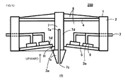
- Fig. 7 is a diagram illustrating a main portion of the structure of a semiconductor device according to a third embodiment.
- Fig. 7(a) is a plan view
- Fig. 7(b) is a side cross-sectional view as viewed from an arrow A of Fig. 7(a)
- Fig. 7(c) is a cross-sectional view illustrating a main portion of an insulating substrate with a conductive pattern.
- a semiconductor device 200 differs from the semiconductor device 100 (see Fig. 1 ) in that a portion of an insulating substrate 5 with a conductive pattern, which is adjacent to a fastener 7, is raised.
- a raised height H is in the range of about 100 ⁇ m to 200 ⁇ m and the upper surface of a sealing resin 8 is also raised by the height. Therefore, the upper surface of the semiconductor device 200 is curved upward in a convex shape by a height of about 100 ⁇ m to 200 ⁇ m.
- Fig. 8 is a diagram illustrating the warping of a back side conductor of the insulating substrate with a conductive pattern shown in Fig. 7 .
- the insulating substrates are curved such that the curve is concave upward.
- a contour line at the center indicates the smallest height (is concave upward) and the height increases concentrically toward the outer circumferential portion.
- warping uniformly occurs from the center to the outer circumference. Therefore, when the semiconductor device 200 is attached to a cooler 11, it is possible to increase the adhesion (contact force) between the insulating substrates 5 with a conductive pattern and the cooler 11.
- Figs. 9 to 10 are diagrams sequentially illustrating processes of attaching the semiconductor device to the cooler.
- the semiconductor device 200 is arranged on the cooler 11.
- the center of a hook portion 7b of the semiconductor device 200 is aligned with an attachment hole 12 provided at the center of the cooler 11.
- the attachment hole 12 has a two-stage structure in which the upper stage is a hole 12a and the lower stage is a hole 12b with a larger diameter than the hole 12a.
- Fig. 9(b) force 13 is applied to a vertex 7e of a post 7a of the fastener 7 to press a hook portion 7b provided at the leading end of the fastener 7 to the hole 12a of the cooler 11.
- a cutout 7d formed in the post 7a is narrowed and the diameter of the hook portion 7b is reduced.
- the hook portion 7b can pass through the hole 12a of the cooler 11.
- a beam portion 4 which is provided on the upper side is distorted downward and a back side conductor 5b of the insulating substrate 5 with a conductive pattern comes into contact with the entire region of the cooler 11.
- the force 13 applied to the fastener 7 which is disposed at the center of the terminal case 1 is transmitted to the center of the cooler 11. Then, the force 13 is transmitted to the outer circumferential portion of the cooler 11. Therefore, strong force is applied to a central portion of the contact surface between the semiconductor device 200 and the cooler 11 and weak force is applied to an outer circumferential portion. Since a corner portion 5d (which is disposed in the vicinity of the fastener 7) of each insulating substrate 5 with a conductive pattern which greatly warps is disposed in the central portion to which strong force is applied, the force applied to the central portion is weakened and uniform force is applied to the entire insulating substrate 5 with a conductive pattern.
- the insulating substrate 5 with a conductive pattern forming the semiconductor device 200 is divided and the insulating substrate 5 with a conductive pattern which is provided in the vicinity of the fastener 7 is raised, it is possible to increase adhesion to the cooler 11. When the adhesion is increased, it is possible to reduce contact thermal resistance between the semiconductor device 200 and the cooler 11.
- the fastener 7 since the fastener 7 is arranged at the center of the terminal case 1 in a plan view, it is possible to reduce the external dimensions of the semiconductor device.
- the hook portion 7b is provided in the fastener 7, it is possible to bring the semiconductor device 200 into close contact with the cooler 11 and to fix the semiconductor device 200 to the cooler 11 with a simple structure. Therefore, a screwing operation requiring a lot of time is not required and torque management is not required. As a result, it is possible to reduce manufacturing costs.
- Figs. 11 to 13 are cross-sectional views illustrating main manufacturing processes of a semiconductor device manufacturing method according to a fourth embodiment.
- Fig. 14 is a diagram illustrating a main portion of the structure of a resin molding jig used in the manufacturing method.
- Fig. 14(a) is a plan view and
- Fig. 14(b) is a cross-sectional view.
- Fig. 14(b) shows a terminal case 1 or an insulating substrate 5 with a conductive pattern for reference.
- the insulating substrates 5 with a conductive pattern are place on a solder jig 21.
- Solder (not shown) is applied onto the insulating substrates 5 (conductive patterns 5a) with a conductive pattern.
- Semiconductor chips 6 are placed on the applied solder.
- solder (not shown) is applied onto the semiconductor chips 6.
- the terminal case 1 in which a beam portion 4 and a fastener 7 are integrally molded is provided on the semiconductor chips 6 such that a leading end 3a of a terminal 3 is provided on the semiconductor chip 6.
- the temperature of the solder jig 21 is increased to melt the solder.
- the solder jig 21 is cooled to solidify the solder such that the insulating substrates 5 with a conductive pattern are soldered to the semiconductor chips 6 and the semiconductor chips 6 are soldered to the terminals 3 (leading ends 3a).
- the terminal case 1 in which the terminals 3 (leading ends 3a) are soldered to the semiconductor chips 6 and the semiconductor chips 6 are soldered to the insulating substrates 5 with a conductive pattern is taken off from the solder jig 21.
- the terminal case 1 in which the terminals 3 (leading ends 3a) are soldered to the semiconductor chips 6 and the semiconductor chips 6 are soldered to the insulating substrates 5 with a conductive pattern is placed on a resin molding jig 24.
- a hole 25 which is formed at the center of the resin molding jig 24 and into which the fastener 7 is inserted has the same structure as an attachment hole 12 which is formed in a cooler 11.
- the resin molding jig 24 can be separated into two portions, that is, the right and left portions (a first jig 24a and a second jig 24b).
- force 26 is applied to a vertex 7e of a post 7a of the fastener 7 to press the fastener 7 downward.
- the beam portion 4 is moved down by about 100 ⁇ m to 200 ⁇ m.
- a hook portion 7b of the fastener 7 passes through a hole 25a and an upper end portion 7f of the hook portion 7b comes into contact with the bottom 25c of the hole 25a formed in the resin molding jig 24.
- the hook portion 7b passes through the hole 25a and is inserted into a hole 25b.
- a cutout 7d is spread and the hook portion 7b returns to the original size.
- a sealing resin 8 is molded in the terminal case 1 and is solidified.
- Fig. 13(f) the force 26 (see Fig. 12 ) is removed and the first jig 24a and the second jig 24b of the resin molding jig 24 shown in Fig. 14 are separated from each other.
- the terminal case 1 in which the sealing resin 8 is molded and solidified is taken off from the resin molding jig 24.
- the beam portion 4 returns to the original position by a spring action and the fastener 7 is raised.
- a corner portion 5d of each of the divided insulating substrates 5 with a conductive pattern, which is adjacent to the fastener 7, is raised toward the terminal case 1 by the spring action of the beam portion 4 so as to be higher than a peripheral portion.
- the raised height H of the corner portion 5d is in the range of about 100 ⁇ m to 200 ⁇ m (in a floating state).
- each insulating substrate 5 with a conductive pattern which is arranged in the vicinity of the fastener 7, is raised, it is possible to improve the contact with the cooler 11.
- FIG. 15 is a cross-sectional view illustrating a main portion of a semiconductor device according to a fifth embodiment.
- a semiconductor device 300 differs from the semiconductor device 200 (see Fig. 7 ) in that a screw 27 replaces the fastener 7.
- a screw thread 28 is formed in the screw 27 and a cross slot 30 is formed in the head 29 of the screw 27.
- the screw 27 is supported by a screw post 31 with a through hole through which the screw 27 passes.
- Fig. 16 is a cross-sectional view illustrating the main portion when the semiconductor device shown in Fig. 15 is attached to a cooler.
- the screw 27 is inserted into a screw receiving portion 11b of a cooler 11a.
- the beam portion 4 is curved downward.
- a sealing resin 8 is interposed and compressed between the beam portion 4 and the insulating substrates 5 with a conductive pattern and presses the insulating substrates 5 with a conductive pattern.
- the pressing force 32 is used to attach the semiconductor device 300 to the cooler 11a.
- the screw thread 28 of the screw 27 is engaged with a screw thread 11c of the screw receiving portion 11b and the screw 27 functions as the hook portion 7b.
- the screw receiving portion 11b is the insertion depth of the screw 27 and the depth is determined such that the repulsive force of the beam portion 4 is appropriate.
- the semiconductor device 300 is not fixed to the cooler 11a by the tightening torque of the screw 27, but by the repulsive force of the beam portion 4 arranged in the terminal case 1. Therefore, torque management for screwing is not required, unlike the related art. In this case, the same effect as that in Embodiment 1 is obtained.
- Fig. 17 is a cross-sectional view illustrating a main portion of a semiconductor device according to a sixth embodiment.
- a semiconductor device 400 differs from the semiconductor device 200 (see Fig. 7 ) in that bonding wires 33 are used as some of the terminals 3 of the terminal case 1.
- the bonding wires 33 are used to connect semiconductor chips 6 and to connect the semiconductor chips 6 and insulating substrates 5 (conductive pattern 5a) with a conductive pattern. Since a fastener 7 of the semiconductor device 400 is the same as that in Embodiment 2, the same effect as that in Embodiment 2 is obtained.
- a general case corresponding to an outer frame 2 of the terminal case 1 is used instead of the terminal case 1 used in Embodiment 6 and the terminal 3 which passes through the terminal case 1 is drawn from the upper side of the general case (outer frame 2) to the outside.
- the application of the bonding wire 33 is not limited to the semiconductor device 200, but the bonding wire 33 can also be applied to the semiconductor devices 100 and 300.
- Embodiments 1 to 4 are summarized as follows.
- the semiconductor devices 100 to 400 are manufactured using the terminal case 1, the beam portion 4 which has elasticity and is connected to the terminal case 1, a plurality of divided insulating substrates 5 with a conductive pattern, the fastener 7 which is provided at the center, and the sealing resin 8 which has elasticity and fills the terminal case 1. Therefore, it is possible to improve adhesion to the coolers 11 and 11a and to reduce contact thermal resistance between the semiconductor devices 100 to 400 and the coolers 11 and 11a.
- the hook portion 7b provided at the leading end of the fastener 7 is inserted into the two-stage holes 12a and 12b provided in the cooler 11 only by a one-touch operation of applying the force 13 to the vertex 7e of the fastener 7. Therefore, it is possible to simply attach the semiconductor devices 100, 200, and 400 to the cooler 11. Since the screw 27 of the semiconductor device 300 is used as the hook portion 7b, it is possible to simply attach the semiconductor device 300 to the cooler 11. The attachment does not require a screwing operation unlike the related art and does not also require torque management. Therefore, it is possible to reduce the manufacturing costs of the semiconductor devices 100, 200, and 400.
- the insulating substrate 5 with a conductive pattern comes into close contact with the cooler 11 and is fixed thereto and the dimensions of the semiconductor device can be reduced, which hold for Embodiments 5 and 6.
Landscapes
- Cooling Or The Like Of Semiconductors Or Solid State Devices (AREA)
Abstract
Description
- The present invention relates to a semiconductor device which is simply attached to a cooler and is manufactured at a low cost, and more particularly to a semiconductor device without a cooling base (for example, a copper base) which comes into contact with a cooler and a semiconductor device manufacturing method.
- In a general semiconductor device, an insulating substrate with a conductive pattern on which a semiconductor chip is mounted is fixed to a cooling base (for example, a copper base) and the cooling base is fixed to a cooler (cooling fin).
- In recent years, a method has been used which directly fixes an insulating substrate with a conductive pattern to a cooler (for example, a cooling fin), without passing through a cooling base, in order to reduce manufacturing costs and thermal resistance in a low-power semiconductor device.
- This semiconductor device is called a copper-base-less type and the insulating substrate with a conductive pattern is one direct copper bonding (DCB) substrate or an aluminum insulating substrate. In addition, for example, a terminal case in which a terminal is attached to a resin case or a case formed by a transfer mold is used as a package and gel (silicon gel) or epoxy resin is used as a sealing resin.
- Three representative examples of a method for attaching the copper-base-less semiconductor device to the cooler according to the related art will be described below.
- 1) There is a method which screws clamps 52 (two positions) which protrude to the outside of a
case 51 of asemiconductor device 500 as shown inFig. 18 (Non-patent Document 1). - 2) There is a method in which
holes 55 through which screws pass are formed at both ends (two positions) of acase 54 of asemiconductor device 600 and thesemiconductor device 600 is screwed, as shown inFig. 19 (Patent Document 1). - 3) There is a method in which a
hole 58 through which a screw passes is formed at the center of acase 57 of asemiconductor device 700 and thesemiconductor device 700 is screwed, as shown inFig. 20 (Patent Document 2). - In the drawings,
reference numerals -
- Patent Document 1:
JP 11-243839 A - Patent Document 2:
US 6979204 - Non-patent Document 1: Infineon, "AN2006-08", Application Note, V2.0, July 2008
- However, in the
semiconductor devices 500 to 700 disclosed inNon-patent Document 1,Patent Document 1, andPatent Document 2, as described above, since the semiconductor device is attached to the cooler only by screws, it is necessary to manage screw tightening torque. - In the
semiconductor devices Non-patent Document 1 andPatent Document 1, since the area of the screw portion for attachment to the cooler is a dead space, the external dimensions of thesemiconductor devices - In the
semiconductor device 500 disclosed inNon-patent Document 1, when the warping of the surface of aback side conductor 53a of aninsulating substrate 53 with a conductive pattern which is not divided is examined, as shown inFig. 21 , the surface warps toward the front side of theinsulating substrate 53 with a conductive pattern and the warping is not necessarily concentrically spread from the center of the semiconductor device. A significant amount of warping may occur in aportion 60 that is separated from the center of theback side conductor 53a. - In
Fig. 21 ,reference numeral 61 indicates a contour line and theportion 60 is lower than other portions. - As such, when the
portion 60 in which a significant amount of warping occurs is separated from the center of theback side conductor 53a, the adhesion between theback side conductor 53a and the cooler is reduced during the attachment of thesemiconductor device 500 to the cooler and the contact thermal resistance between thesemiconductor device 500 and the cooler increases. In addition, in some cases, a thermal grease is applied onto a contact surface between thesemiconductor device 500 and the cooler in order to prevent an increase in the contact thermal resistance. However, in the portion in which a large amount of warping occurs, the amount of thermal grease applied increases and thermal resistance increases. - The
semiconductor devices 500 to 700 disclosed in the above-mentioned three patent documents will be described in detail below. - 1) In the
semiconductor devices
That is, in thesemiconductor devices - 2) In the
semiconductor devices cases - 3) Since one
insulating substrate semiconductor device 500, a significant amount of warping occurs in theinsulating substrate 53 with a conductive pattern. - 4) As described in 3), since the shape of the warping of the
insulating substrates semiconductor device semiconductor device - The invention has been made in order to solve the above-mentioned problems and an object of the invention is to provide a semiconductor device which is closely attached to a cooler with a simple structure, without torque management, and can reduce contact thermal resistance, external dimensions, and manufacturing costs and a semiconductor device manufacturing method.
- In order to achieve the object of the invention, according to a first aspect of the invention, a semiconductor device includes: a plurality of insulating substrates with a conductive pattern, each of which includes a conductor formed on a main surface of an insulating plate; a case which accommodates the plurality of insulating substrates with a conductive pattern such that one main surface of each of the insulating substrates with a conductive pattern is exposed and to which a cooler that comes into contact with the exposed main surface of each of the plurality of insulating substrates with a conductive pattern is attached; a beam portion that is provided in the case in a beam shape so as to face the other main surfaces of the plurality of insulating substrates with a conductive pattern accommodated in the case; and a fastener that has a post shape, is provided at the center of the beam portion, and has a leading end which is inserted into an attachment hole of the cooler attached to the case such that the beam portion is distorted.
- According to a second aspect of the invention, the semiconductor device according to the first aspect may further include a sealing resin that fills the case so as to come into contact with the plurality of insulating substrates with a conductive pattern and the beam portion.
- According to a third aspect of the invention, in the semiconductor device according to the second aspect, the sealing resin may be made of an elastic material.
- According to a fourth aspect of the invention, in the semiconductor device according to the first aspect, the plurality of insulating substrates with a conductive pattern may be accommodated in the case so as to surround the fastener having the leading end attached to the cooler.
- According to a fifth aspect of the invention, in the semiconductor device according to the third aspect, the plurality of insulating substrates with a conductive pattern may be raised toward the beam portion such that a portion thereof close to the fastener is higher than an outer circumferential portion close to the case.
- According to a sixth aspect of the invention, in the semiconductor device according to the first or second aspect, the case, the beam portion, and the fastener may be integrally formed of a resin by molding.
- According to a seventh aspect of the invention, in the semiconductor device according to the first aspect, the fastener may include a post and a hook portion which is provided at a leading end of the post and a cutout may be formed in the post so as to extend from the bottom of the hook portion.
- According to an eighth aspect of the invention, in the semiconductor device according to the first aspect, the plurality of insulating substrates with a conductive pattern may be formed by radially dividing a large insulating substrate with a conductive pattern.
- According to a ninth aspect of the invention, in the semiconductor device according to the first aspect, a screw may be formed at the leading end of the fastener.
- According to a tenth aspect of the invention, a semiconductor device manufacturing method includes: a step of placing a plurality of insulating substrates with a conductive pattern, each of which includes a conductor formed on a main surface of an insulating plate, on a jig such that the plurality of insulating substrates with a conductive pattern surround a central hole of the jig and one main surface of each of the plurality of insulating substrates with a conductive pattern faces the jig; and a step of covering the plurality of insulating substrates with a conductive pattern with a terminal case, in which a case which accommodates the plurality of insulating substrates with a conductive pattern such that the one main surface of each of the insulating substrates with a conductive pattern is exposed and to which a cooler that comes into contact with the exposed main surface of each of the plurality of insulating substrates with a conductive pattern is attached, a beam portion that is provided in the case in a beam shape so as to face the other main surfaces of the plurality of insulating substrates with a conductive pattern accommodated in the case, and a fastener that has a post shape, is provided at the center of the beam portion, and has a leading end which is inserted into an attachment hole of the cooler attached to the case such that the beam portion is distorted are integrally molded, such that the leading end of the fastener is aligned with the central hole of the jig.
- According to an eleventh aspect of the invention, the semiconductor device manufacturing method according to the tenth aspect may further include a step of filling the terminal case which covers the plurality of insulating substrate with a conductive pattern with a sealing resin and solidifying the sealing resin which comes into contact with the plurality of insulating substrate with a conductive pattern and the beam portion.
- According to a twelfth aspect of the invention, the semiconductor device manufacturing method according to the eleventh aspect may further include a step of pressing the center of the beam portion against the jig to insert the leading end of the fastener into an insertion hole of the jig, thereby distorting the beam portion, before the terminal case is filled with the sealing resin.
- According to a thirteenth aspect of the invention, the semiconductor device manufacturing method according to the twelfth aspect may further include a step of dividing the jig into two parts along a cutting line which passes through the insertion hole provided at the center of the jig and returning the distorted beam portion to the original position, after the beam portion is distorted and the sealing resin is solidified.
- According to the invention, the semiconductor device includes the insulating substrates with a conductive pattern, the case which accommodates the insulating substrates with a conductive pattern such that one main surface of each of the insulating substrates with a conductive pattern is exposed and is attached to the cooler, and the beam portion that is provided in the case in the beam shape so as to face the other main surfaces of the insulating substrates with a conductive pattern. The leading end of the fastener that has a post shape and is provided at the center of the beam portion is inserted into the attachment hole of the cooler attached to the case such that the beam portion is distorted. Therefore, it is possible to increase adhesion to the cooler and to reduce contact thermal resistance.
- The sealing resin fills the case so as to come into contact with the plurality of insulating substrates with a conductive pattern and the beam portion. Therefore, the semiconductor device can be closely attached to the cooler.
- The plurality of insulating substrates with a conductive pattern surround the fastener having the leading end attached to the cooler and are raised toward the beam portion such that the a portion thereof close to the fastener is higher than an outer circumferential portion close to the case. Therefore, the semiconductor device can be simply attached to the cooler by a one-touch operation. The attachment does not require torque management which is required for screwing and it is possible to provide an inexpensive semiconductor device.
- Since the attachment portion is disposed at the center of the case, it is possible to reduce the external dimensions, as compared to the related art in which the attachment portion is disposed in the outer circumferential portion. Therefore, it is possible to provide a small semiconductor device.
- The above and other objects, features, and advantages of the invention will become apparent from the following detailed description taken with the accompanying drawings indicating the preferred embodiments of the invention.
-
-
Fig. 1 is a diagram illustrating a main portion of the structure of a semiconductor device according to a first embodiment.Fig. 1(a) is a plan view,Fig. 1(b) is a side cross-sectional view as viewed from an arrow A ofFig. 1(a), and Fig. 1(c) is a cross-sectional view illustrating a main portion of an insulating substrate with a conductive pattern; -
Fig. 2 is a plan view illustrating the main portion of the insulating substrate with a conductive pattern in a terminal case shown inFig. 1 ; -
Fig. 3 is a diagram sequentially illustrating processes of attaching the semiconductor device to a cooler; -
Fig. 4 is a diagram sequentially illustrating the processes of attaching the semiconductor device to the cooler, which followsFig. 3 ; -
Fig. 5 is a cross-sectional view sequentially illustrating main manufacturing processes of a semiconductor device manufacturing method according to a second embodiment; -
Fig. 6 is a diagram sequentially illustrating the main manufacturing processes of the semiconductor device manufacturing method according to the second embodiment, which followsFig. 5 ; -
Fig. 7 is a diagram illustrating a main portion of the structure of a semiconductor device according to a third embodiment.Fig. 7(a) is a plan view,Fig. 7(b) is a side cross-sectional view as viewed from an arrow A ofFig. 7(a), and Fig. 7(c) is a cross-sectional view illustrating a main portion of an insulating substrate with a conductive pattern; -
Fig. 8 is a diagram illustrating the warping of a back side conductor of the insulating substrate with a conductive pattern shown inFig. 7 ; -
Fig. 9 is a diagram sequentially illustrating a process of attaching the semiconductor device to a cooler; -
Fig. 10 is a diagram illustrating the process of attaching the semiconductor device to the cooler, which followsFig. 9 ; -
Fig. 11 is a cross-sectional view sequentially illustrating main manufacturing processes of a semiconductor device manufacturing method according to a fourth embodiment; -
Fig. 12 is a cross-sectional view sequentially illustrating the main manufacturing processes of the semiconductor device manufacturing method according to the fourth embodiment, which followsFig. 11 ; -
Fig. 13 is a cross-sectional view sequentially illustrating the main manufacturing processes of the semiconductor device manufacturing method according to the fourth embodiment, which followsFig. 12 ; -
Fig. 14 is a diagram illustrating a main portion of the structure of a resin molding jig used in the manufacturing method.Fig. 14(a) is a plan view andFig. 14(b) is a cross-sectional view; -
Fig. 15 is a cross-sectional view illustrating a main portion of the structure of a semiconductor device according to a fifth embodiment; -
Fig. 16 is a diagram illustrating a main portion when the semiconductor device shown inFig. 15 is attached to a cooler; -
Fig. 17 is a cross-sectional view illustrating a main portion of the structure of a semiconductor device according to a sixth embodiment; -
Fig. 18 is a diagram illustrating a main portion of the structure of a semiconductor device disclosed inNon-patent Document 1.Fig. 18(a) is a side view andFig. 18(b) is a top view; -
Fig. 19 is a diagram illustrating a main portion of the structure of a semiconductor device disclosed inPatent Document 1.Fig. 19(a) is a side view andFig. 19(b) is a top view; -
Fig. 20 is a diagram illustrating a main portion of the structure of a semiconductor device disclosed inPatent Document 2.Fig. 20(a) is a side view andFig. 20(b) is a top view; and -
Fig. 21 is a diagram illustrating the warping of a back side conductor shown inFig. 18 . - Embodiments of the invention will be described.
-
Fig. 1 is a diagram illustrating a main portion of the structure of a semiconductor device according to a first embodiment.Fig. 1(a) is a plan view,Fig. 1(b) is a side cross-sectional view as viewed from an arrow A ofFig. 1(a), and Fig. 1(c) is a cross-sectional view illustrating a main portion of an insulating substrate with a conductive pattern. - A
semiconductor device 100 includes aterminal case 1 in whichterminals 3, which are external lead terminals, are fixed to anouter frame 2, which is a case, and across-shaped beam portion 4 that is connected to theterminal case 1 and has elasticity (spring action). Thesemiconductor device 100 includes four divided insulatingsubstrates 5 with a conductive pattern andsemiconductor chips 6 that are fixed to each insulatingsubstrate 5 with a conductive pattern. The insulatingsubstrate 5 with a conductive pattern has a size of, for example, 20 mm x 30 mm. In addition, thesemiconductor device 100 includes afastener 7 that is fixed to the center of thebeam portion 4 and protrudes to the lower side of the insulatingsubstrate 5 with a conductive pattern and a sealingresin 8 that fills theterminal case 1 and has elasticity. Theterminal case 1, thebeam portion 4, and thefastener 7 are formed of the same resin material (for example, PBT: polybutylene terephthalate) by molding. Each of theterminal case 1, thebeam portion 4, and thefastener 7 may be fixed by an adhesive. Since thebeam portion 4 has a spring action, it has a small thickness of, for example, about 1 mm. In addition, thebeam portion 4 has a width of a few millimeters, for example, 4 mm. Theterminal 3 is a connection conductor plate with a small width. - The
leading end 3a of the terminal 3 (external lead terminal) in theterminal case 1 is fixed to thesemiconductor chip 6 or the insulatingsubstrate 5 with a conductive pattern by solder (not shown). Thesemiconductor chip 6 is fixed to aconductive pattern 5a (Fig. 1(c) ) of the insulatingsubstrate 5 with a conductive pattern by solder (not shown). A material with high adhesion between theterminal case 1 and the insulatingsubstrate 5 with a conductive pattern is used as the sealingresin 8 that has elasticity and fills theterminal case 1. For example, a bonding material with high adhesion may be used. Specifically, for example, RTV Rubber manufactured by Shin-Etsu Chemical Co., Ltd. is used. The insulatingsubstrate 5 with a conductive pattern and the inner wall of theterminal case 1 do not come into close contact with each other, but may come into loose contact with each other or may have a gap therebetween. The contact makes it possible for the insulatingsubstrate 5 with a conductive pattern to be moved by the viscosity of the sealingresin 8 when thesemiconductor device 100 is attached to a cooler 11, which will be described below. The relationship between the insulatingsubstrate 5 with a conductive pattern and the inner wall of theterminal case 1 and the relationship between the insulatingsubstrate 5 with a conductive pattern and the sealingresin 8 hold forEmbodiments 2 to 6, which will be described below. - A
back side conductor 5b (Fig. 1(c) ) of each insulatingsubstrate 5 with a conductive pattern is little curved and is flat. - In
Embodiment 1, four divided insulatingsubstrates 5 with a conductive pattern are provided. However, two divided insulatingsubstrates 5 with a conductive pattern may be provided. That is, the insulatingsubstrate 5 with a conductive pattern may be divided into a plurality of insulating substrates along lines which radially extend from the center of theterminal case 1. As shown inFig. 1(c) , the insulatingsubstrate 5 with a conductive pattern includes an insulatingsubstrate 5c, such as a ceramic plate, theconductive pattern 5a which is a conductor formed on the front surface of the insulatingsubstrate 5c, and aback side conductor 5b which is formed on the back side. As described above, thesemiconductor chip 6 is soldered to theconductive pattern 5a and theback side conductor 5b comes into pressure contact with a cooler (not shown). - The
fastener 7 includes apost 7a and ahook portion 7b that is provided at the lower end of thepost 7a. Acutout 7d is formed in thepost 7a so as to extend from the bottom 7c of thehook portion 7b in the longitudinal direction (downward direction). Thecutout 7d is used to fix thesemiconductor device 100 to the cooler (not shown) through thefastener 7. Thehook portion 7b is formed such that the cross-sectional area thereof increases toward the upper side. InFig. 1 , thecutout 7d is formed in one direction from the front side to the rear side of the plane of paper. However, thecutout 7d may also be formed along the central axis of thepost 7a in a direction perpendicular to thecutout 7d. In addition, a plurality of cutouts may be formed along the central axis of thepost 7a so as to intersect each other. The structure of the cutout holds forEmbodiments 2 to 4 andEmbodiment 6. -
Fig. 2 is a plan view illustrating the arrangement of the insulating substrates with a conductive pattern in the terminal case shown inFig. 1 . InFig. 2 , thebeam portion 4 and thefastener 7 are not shown. Four divided insulatingsubstrates 5 with a conductive pattern are arranged around thecenter 9 where thefastener 7 is provided. A dividingline 10 by which the insulating substrate with a conductive pattern is divided into four insulatingsubstrates 5 with a conductive pattern extends radially (here, in a cross shape) from the position of thefastener 7. That is, the divided insulatingsubstrates 5 with a conductive pattern are radially arranged from thefastener 7. -
Figs. 3 and4 are diagrams sequentially illustrating a process of attaching the semiconductor device to the cooler. - In
Fig. 3(a) , thesemiconductor device 100 is arranged on a cooler 11. In this case, the center of thehook portion 7b of thesemiconductor device 100 is aligned with anattachment hole 12 provided at the center of the cooler 11. Theattachment hole 12 has a two-stage structure in which the upper stage is ahole 12a and the lower stage is ahole 12b with a larger diameter than thehole 12a. The diameter of thehole 12a is equal to or greater than a value obtained by subtracting the width dd of thecutout 7d from the maximum diameter AA of thehook portion 7b and is less than the maximum diameter AA of thehook portion 7b. The diameter of thehole 12b is equal to or greater than the maximum diameter AA of thehook portion 7b. The structure of theholes Embodiments 2 to 4 andEmbodiment 6. - In
Fig. 3(b) ,force 13 is applied to avertex 7e of thepost 7a of thefastener 7 to press thehook portion 7b provided at the leading end of thefastener 7 to thehole 12a of the cooler 11. In this case, thecutout 7d formed in thepost 7a is narrowed and the diameter of thehook portion 7b is reduced. Thehook portion 7b can pass through thehole 12a of the cooler 11. In this case, thebeam portion 4 is distorted downward and the sealingresin 8 interposed between thebeam portion 4, which is an elastic body, and the insulatingsubstrate 5 with a conductive pattern is compressed. - In
Fig. 4(c) , after thehook portion 7b passes through thehole 12a of the cooler 11, thecutout 7d is spread by a spring action and returns to the original size. The sealingresin 8 is compressed by theforce 13 andrepulsive force 14 is applied in all directions like hydrostatic pressure. - In
Fig. 4(d) , when theforce 13 applied to thevertex 7e of thefastener 7 is removed, thebeam portion 4 which is distorted downward is raised by the spring action and force to return thebeam portion 4 and thecompressed sealing resin 8 to the original state acts as therepulsive force 14 andrepulsive force 15. In this case, since thecompressed sealing resin 8 does not return to the original state, therepulsive force 14 applied to the sealingresin 8 is maintained. Therepulsive force 14 presses the insulatingsubstrates 5 with a conductive pattern to the lower side. When thebeam portion 4 is drawn to the upper side by therepulsive force 15, anupper end portion 7f of thehook portion 7b provided at the leading end of thefastener 7 presses the bottom 12c of thehole 12a of the cooler 11. Therepulsive force 15 of thebeam portion 4 is transmitted to the cooler 11 through thefastener 7 and the cooler 11 is pressed upward. The insulatingsubstrates 5 with a conductive pattern are pressed byforce 16. The insulatingsubstrates 5 with a conductive pattern come into close contact with the cooler 11 and are fixed thereto by therepulsive force 14 of the sealingresin 8 and theforce 16 to raise the cooler 11. As such, since thehook portion 7b is formed at the leading end of thefastener 7, thehook portion 7b is inserted into thehole 12 of the cooler 11 only by a one-touch operation of applying theforce 13 to thevertex 7e of thefastener 7. It is possible to bring thesemiconductor device 100 into close contact with the cooler 11 and to fix thesemiconductor device 100 to the cooler 11 with a simple structure. - Since the insulating
substrate 5 with a conductive pattern forming thesemiconductor device 100 is divided, it is possible to increase adhesion to the cooler 11 and to reduce contact thermal resistance. In addition, in thesemiconductor device 100, since thefastener 7 is arranged at the center of theterminal case 1 in a plan view, it is possible to reduce the external dimensions of the semiconductor device, as compared to the semiconductor device disclosed inNon-patent Document 1 orPatent Document 1. In addition, in thesemiconductor device 100, since thehook portion 7b is provided in thefastener 7, it is possible to bring thesemiconductor device 100 into close contact with the cooler 11 and to fix thesemiconductor device 100 to the cooler 11 with a simple structure. Therefore, a screwing operation requiring a lot of time is not required and torque management is not required. As a result, it is possible to reduce manufacturing costs. -
Figs. 5 and6 are cross-sectional views sequentially illustrating main manufacturing processes of a semiconductor device manufacturing method according to a second embodiment. - In
Fig. 5(a) , insulatingsubstrates 5 with a conductive pattern are placed on asolder jig 21. Solder (not shown) is applied onto the insulating substrates 5 (conductive patterns 5a) with a conductive pattern.Semiconductor chips 6 are placed on the applied solder. - In
Fig. 5(b) , solder (not shown) is applied onto thesemiconductor chips 6. Aterminal case 1 in which abeam portion 4 and afastener 7 are integrally molded is provided on thesemiconductor chips 6 such that aleading end 3a of a terminal 3 (external lead terminal) is provided on thesemiconductor chip 6. Then, the temperature of thesolder jig 21 is increased to melt the solder. Then, thesolder jig 21 is cooled to solidify the solder such that the insulatingsubstrates 5 with a conductive pattern are soldered to thesemiconductor chips 6 and thesemiconductor chips 6 are soldered to the terminals 3 (leading ends 3a). - In
Fig. 5(c) , theterminal case 1 in which the terminals 3 (leading ends 3a) are soldered to thesemiconductor chips 6 and thesemiconductor chips 6 are soldered to the insulatingsubstrates 5 with a conductive pattern is taken off from thesolder jig 21. - In
Fig. 6(d) , theterminal case 1 after soldering is placed on aresin molding jig 22 and the sealingresin 8 is molded and solidified. The sealingresin 8 is the existing resin with elasticity and is, for example, a bonding material with high adhesion. - In
Fig. 6(e) , theterminal case 1 in which the sealingresin 8 is molded and solidified is taken off from theresin molding jig 22. - In the
semiconductor device 100, the entire exposed surface of aback side conductor 5b of each of the four divided insulatingsubstrates 5 with a conductive pattern is flat (seeFig. 1 ). Therefore, when thesemiconductor device 100 is attached to a cooler 11, a contact force tends to increase in the vicinity of thefastener 7 and to decrease in an outer circumferential portion in the contact surface between thesemiconductor device 100 and the cooler 11. A method which solves the problem and can fix the semiconductor device from the vicinity of thefastener 7 to the outer circumferential portion will be described below. -
Fig. 7 is a diagram illustrating a main portion of the structure of a semiconductor device according to a third embodiment.Fig. 7(a) is a plan view,Fig. 7(b) is a side cross-sectional view as viewed from an arrow A ofFig. 7(a), and Fig. 7(c) is a cross-sectional view illustrating a main portion of an insulating substrate with a conductive pattern. - A
semiconductor device 200 differs from the semiconductor device 100 (seeFig. 1 ) in that a portion of an insulatingsubstrate 5 with a conductive pattern, which is adjacent to afastener 7, is raised. A raised height H is in the range of about 100 µm to 200 µm and the upper surface of a sealingresin 8 is also raised by the height. Therefore, the upper surface of thesemiconductor device 200 is curved upward in a convex shape by a height of about 100 µm to 200 µm. -
Fig. 8 is a diagram illustrating the warping of a back side conductor of the insulating substrate with a conductive pattern shown inFig. 7 . The insulating substrates are curved such that the curve is concave upward. InFig. 8 , among contours line 23 of the curve, a contour line at the center indicates the smallest height (is concave upward) and the height increases concentrically toward the outer circumferential portion. As such, warping uniformly occurs from the center to the outer circumference. Therefore, when thesemiconductor device 200 is attached to a cooler 11, it is possible to increase the adhesion (contact force) between the insulatingsubstrates 5 with a conductive pattern and the cooler 11. -
Figs. 9 to 10 are diagrams sequentially illustrating processes of attaching the semiconductor device to the cooler. - In
Fig. 9(a) , thesemiconductor device 200 is arranged on the cooler 11. In this case, the center of ahook portion 7b of thesemiconductor device 200 is aligned with anattachment hole 12 provided at the center of the cooler 11. Theattachment hole 12 has a two-stage structure in which the upper stage is ahole 12a and the lower stage is ahole 12b with a larger diameter than thehole 12a. - In
Fig. 9(b) ,force 13 is applied to avertex 7e of apost 7a of thefastener 7 to press ahook portion 7b provided at the leading end of thefastener 7 to thehole 12a of the cooler 11. In this case, acutout 7d formed in thepost 7a is narrowed and the diameter of thehook portion 7b is reduced. Thehook portion 7b can pass through thehole 12a of the cooler 11. In this case, abeam portion 4 which is provided on the upper side is distorted downward and aback side conductor 5b of the insulatingsubstrate 5 with a conductive pattern comes into contact with the entire region of the cooler 11. - In
Fig. 10(c) , after thehook portion 7b passes through thehole 12a of the cooler 11, thecutout 7d is spread and returns to the original state. Thecutout 7d returns to the original size. - In
Fig. 10(d) , when theforce 13 applied to thevertex 7e of thefastener 7 is removed, thebeam portion 4 which is distorted downward is raised by a spring action and force to return thebeam portion 4 to the original state acts. Theforce 15 is transmitted to thehook portion 7b provided at the leading end of thefastener 7 and anupper end portion 7f of thehook portion 7b comes into close contact with the bottom 12c of thehole 12a of the cooler 11.Repulsive force 14 generated by the spring action of thebeam portion 4 is transmitted to the cooler 11 through thehook portion 7b and the cooler 11 is raised. The insulatingsubstrate 5 with a conductive pattern is pressed by therepulsive force 14 generated by the sealingresin 8. In this way, thesemiconductor device 200 comes into close contact with the cooler 11 and is fixed thereto. - In the
semiconductor device 200, theforce 13 applied to thefastener 7 which is disposed at the center of theterminal case 1 is transmitted to the center of the cooler 11. Then, theforce 13 is transmitted to the outer circumferential portion of the cooler 11. Therefore, strong force is applied to a central portion of the contact surface between thesemiconductor device 200 and the cooler 11 and weak force is applied to an outer circumferential portion. Since acorner portion 5d (which is disposed in the vicinity of the fastener 7) of each insulatingsubstrate 5 with a conductive pattern which greatly warps is disposed in the central portion to which strong force is applied, the force applied to the central portion is weakened and uniform force is applied to the entire insulatingsubstrate 5 with a conductive pattern. - In addition, since the insulating
substrate 5 with a conductive pattern forming thesemiconductor device 200 is divided and the insulatingsubstrate 5 with a conductive pattern which is provided in the vicinity of thefastener 7 is raised, it is possible to increase adhesion to the cooler 11. When the adhesion is increased, it is possible to reduce contact thermal resistance between thesemiconductor device 200 and the cooler 11. In addition, in thesemiconductor device 200, since thefastener 7 is arranged at the center of theterminal case 1 in a plan view, it is possible to reduce the external dimensions of the semiconductor device. In addition, in thesemiconductor device 200, since thehook portion 7b is provided in thefastener 7, it is possible to bring thesemiconductor device 200 into close contact with the cooler 11 and to fix thesemiconductor device 200 to the cooler 11 with a simple structure. Therefore, a screwing operation requiring a lot of time is not required and torque management is not required. As a result, it is possible to reduce manufacturing costs. -
Figs. 11 to 13 are cross-sectional views illustrating main manufacturing processes of a semiconductor device manufacturing method according to a fourth embodiment. -
Fig. 14 is a diagram illustrating a main portion of the structure of a resin molding jig used in the manufacturing method.Fig. 14(a) is a plan view andFig. 14(b) is a cross-sectional view.Fig. 14(b) shows aterminal case 1 or an insulatingsubstrate 5 with a conductive pattern for reference. - In
Fig. 11(a) , the insulatingsubstrates 5 with a conductive pattern are place on asolder jig 21. Solder (not shown) is applied onto the insulating substrates 5 (conductive patterns 5a) with a conductive pattern.Semiconductor chips 6 are placed on the applied solder. - In
Fig. 11(b) , solder (not shown) is applied onto thesemiconductor chips 6. Theterminal case 1 in which abeam portion 4 and afastener 7 are integrally molded is provided on thesemiconductor chips 6 such that aleading end 3a of aterminal 3 is provided on thesemiconductor chip 6. Then, the temperature of thesolder jig 21 is increased to melt the solder. Then, thesolder jig 21 is cooled to solidify the solder such that the insulatingsubstrates 5 with a conductive pattern are soldered to thesemiconductor chips 6 and thesemiconductor chips 6 are soldered to the terminals 3 (leading ends 3a). - In
Fig. 11(c) , theterminal case 1 in which the terminals 3 (leading ends 3a) are soldered to thesemiconductor chips 6 and thesemiconductor chips 6 are soldered to the insulatingsubstrates 5 with a conductive pattern is taken off from thesolder jig 21. - In
Fig. 12(d) , theterminal case 1 in which the terminals 3 (leading ends 3a) are soldered to thesemiconductor chips 6 and thesemiconductor chips 6 are soldered to the insulatingsubstrates 5 with a conductive pattern is placed on aresin molding jig 24. Ahole 25 which is formed at the center of theresin molding jig 24 and into which thefastener 7 is inserted has the same structure as anattachment hole 12 which is formed in a cooler 11. However, as shown inFig. 14 , theresin molding jig 24 can be separated into two portions, that is, the right and left portions (afirst jig 24a and asecond jig 24b). - Then, force 26 is applied to a
vertex 7e of apost 7a of thefastener 7 to press thefastener 7 downward. Then, thebeam portion 4 is moved down by about 100 µm to 200 µm. Ahook portion 7b of thefastener 7 passes through ahole 25a and anupper end portion 7f of thehook portion 7b comes into contact with the bottom 25c of thehole 25a formed in theresin molding jig 24. - In
Fig. 12(e) , thehook portion 7b passes through thehole 25a and is inserted into ahole 25b. When thehook portion 7b is inserted into thehole 25b, acutout 7d is spread and thehook portion 7b returns to the original size. Withforce 26 being applied, a sealingresin 8 is molded in theterminal case 1 and is solidified. - In
Fig. 13(f) , the force 26 (seeFig. 12 ) is removed and thefirst jig 24a and thesecond jig 24b of theresin molding jig 24 shown inFig. 14 are separated from each other. Theterminal case 1 in which the sealingresin 8 is molded and solidified is taken off from theresin molding jig 24. In this case, since theforce 26 is removed, thebeam portion 4 returns to the original position by a spring action and thefastener 7 is raised. Acorner portion 5d of each of the divided insulatingsubstrates 5 with a conductive pattern, which is adjacent to thefastener 7, is raised toward theterminal case 1 by the spring action of thebeam portion 4 so as to be higher than a peripheral portion. The raised height H of thecorner portion 5d is in the range of about 100 µm to 200 µm (in a floating state). - As such, since the
corner portion 5d of each insulatingsubstrate 5 with a conductive pattern, which is arranged in the vicinity of thefastener 7, is raised, it is possible to improve the contact with the cooler 11. -
Fig. 15 is a cross-sectional view illustrating a main portion of a semiconductor device according to a fifth embodiment. Asemiconductor device 300 differs from the semiconductor device 200 (seeFig. 7 ) in that ascrew 27 replaces thefastener 7. Ascrew thread 28 is formed in thescrew 27 and across slot 30 is formed in thehead 29 of thescrew 27. Thescrew 27 is supported by ascrew post 31 with a through hole through which thescrew 27 passes. -
Fig. 16 is a cross-sectional view illustrating the main portion when the semiconductor device shown inFig. 15 is attached to a cooler. Thescrew 27 is inserted into ascrew receiving portion 11b of a cooler 11a. When thescrew 27 is tightened, thebeam portion 4 is curved downward. In this case, a sealingresin 8 is interposed and compressed between thebeam portion 4 and the insulatingsubstrates 5 with a conductive pattern and presses the insulatingsubstrates 5 with a conductive pattern. The pressingforce 32 is used to attach thesemiconductor device 300 to the cooler 11a. Thescrew thread 28 of thescrew 27 is engaged with ascrew thread 11c of thescrew receiving portion 11b and thescrew 27 functions as thehook portion 7b. Thescrew receiving portion 11b is the insertion depth of thescrew 27 and the depth is determined such that the repulsive force of thebeam portion 4 is appropriate. - The
semiconductor device 300 is not fixed to the cooler 11a by the tightening torque of thescrew 27, but by the repulsive force of thebeam portion 4 arranged in theterminal case 1. Therefore, torque management for screwing is not required, unlike the related art. In this case, the same effect as that inEmbodiment 1 is obtained. -
Fig. 17 is a cross-sectional view illustrating a main portion of a semiconductor device according to a sixth embodiment. Asemiconductor device 400 differs from the semiconductor device 200 (seeFig. 7 ) in thatbonding wires 33 are used as some of theterminals 3 of theterminal case 1. In this embodiment, thebonding wires 33 are used to connectsemiconductor chips 6 and to connect thesemiconductor chips 6 and insulating substrates 5 (conductive pattern 5a) with a conductive pattern. Since afastener 7 of thesemiconductor device 400 is the same as that inEmbodiment 2, the same effect as that inEmbodiment 2 is obtained. In some cases, a general case corresponding to anouter frame 2 of theterminal case 1 is used instead of theterminal case 1 used inEmbodiment 6 and theterminal 3 which passes through theterminal case 1 is drawn from the upper side of the general case (outer frame 2) to the outside. - The application of the
bonding wire 33 is not limited to thesemiconductor device 200, but thebonding wire 33 can also be applied to thesemiconductor devices - The above-described
Embodiments 1 to 4 are summarized as follows. - The
semiconductor devices 100 to 400 are manufactured using theterminal case 1, thebeam portion 4 which has elasticity and is connected to theterminal case 1, a plurality of divided insulatingsubstrates 5 with a conductive pattern, thefastener 7 which is provided at the center, and the sealingresin 8 which has elasticity and fills theterminal case 1. Therefore, it is possible to improve adhesion to thecoolers semiconductor devices 100 to 400 and thecoolers - Since a plurality of divided insulating
substrates 5 with a conductive pattern are provided, they can be closely attached to thecoolers - In the
semiconductor devices hook portion 7b provided at the leading end of thefastener 7 is inserted into the two-stage holes force 13 to thevertex 7e of thefastener 7.
Therefore, it is possible to simply attach thesemiconductor devices screw 27 of thesemiconductor device 300 is used as thehook portion 7b, it is possible to simply attach thesemiconductor device 300 to the cooler 11. The attachment does not require a screwing operation unlike the related art and does not also require torque management.
Therefore, it is possible to reduce the manufacturing costs of thesemiconductor devices - In
Embodiments 1 to 4, the insulatingsubstrate 5 with a conductive pattern comes into close contact with the cooler 11 and is fixed thereto and the dimensions of the semiconductor device can be reduced, which hold forEmbodiments - Only the principle of the invention has been described above. Various modifications and changes of the invention can be made by those skilled in the art. The invention is not limited to the above-mentioned accurate structures and applications and all of the corresponding modifications and equivalents are regarded as the scope of the invention defined by the appended claims and equivalents thereof.
-
- 1
- TERMINAL CASE
- 2
- OUTER FRAME
- 3
- TERMINAL
- 4
- BEAM PORTION
- 5
- INSULATING SUBSTRATE WITH CONDUCTIVE PATTERN
- 5a
- CONDUCTIVE PATTERN
- 5b
- BACK SIDE CONDUCTOR
- 5c
- INSULATING SUBSTRATE
- 6
- SEMICONDUCTOR CHIP
- 7
- FASTENER
- 7a
- POST
- 7b
- HOOK PORTION
- 7c
- BOTTOM
- 7d
- CUTOUT
- 7e
- VERTEX
- 8
- SEALING RESIN
- 9
- CENTER
- 10
- DIVIDING LINE
- 11, 11a
- COOLER
- 12
- ATTACHMENT HOLE
- 12a, 25a
- SMALL HOLE
- 12b, 25b
- LARGE HOLE
- 13, 16, 26, 32
- FORCE
- 14,
- 15 REPULSIVE FORCE
- 21
- SOLDER JIG
- 22, 24
- RESIN MOLDING JIG
- 23
- CONTOUR LINE
- 24a
- FIRST JIG
- 24b
- SECOND JIG
- 25
- INSERTION HOLE
- 27
- SCREW
- 28
- SCREW THREAD
- 29
- HEAD
- 30
- CROSS SLOT
- 31
- SCREW POST
- 33
- BONDING WIRE
Claims (13)
- A semiconductor device comprising:a plurality of insulating substrates with a conductive pattern, each of which includes a conductor formed on a main surface of an insulating plate;a case which accommodates the plurality of insulating substrates with a conductive pattern such that one main surface of each of the insulating substrates with a conductive pattern is exposed and to which a cooler that comes into contact with the exposed main surface of each of the plurality of insulating substrates with a conductive pattern is attached;a beam portion that is provided in the case in a beam shape so as to face the other main surfaces of the plurality of insulating substrates with a conductive pattern accommodated in the case; anda fastener that has a post shape, is provided at the center of the beam portion, and has a leading end which is inserted into an attachment hole of the cooler attached to the case such that the beam portion is distorted.
- The semiconductor device according to claim 1, further comprising:a sealing resin that fills the case so as to come into contact with the plurality of insulating substrates with a conductive pattern and the beam portion.
- The semiconductor device according to claim 2,
wherein the sealing resin is made of an elastic material. - The semiconductor device according to claim 1,
wherein the plurality of insulating substrates with a conductive pattern are accommodated in the case so as to surround the fastener having the leading end attached to the cooler. - The semiconductor device according to claim 3,
wherein the plurality of insulating substrates with a conductive pattern are raised toward the beam portion such that a portion thereof close to the fastener is higher than an outer circumferential portion close to the case. - The semiconductor device according to claim 1,
wherein the case, the beam portion, and the fastener are integrally formed of a resin by molding. - The semiconductor device according to claim 1,
wherein the fastener includes a post and a hook portion which is provided at a leading end of the post, and
a cutout is formed in the post so as to extend from the bottom of the hook portion. - The semiconductor device according to claim 1,
wherein the plurality of insulating substrates with a conductive pattern are formed by radially dividing a large insulating substrate with a conductive pattern. - The semiconductor device according to claim 1,
wherein a screw is formed at the leading end of the fastener. - A semiconductor device manufacturing method comprising:a step of placing a plurality of insulating substrates with a conductive pattern, each of which includes a conductor formed on a main surface of an insulating plate, on a jig such that the plurality of insulating substrates with a conductive pattern surround a central hole of the jig and one main surface of each of the plurality of insulating substrates with a conductive pattern faces the jig; anda step of covering the plurality of insulating substrates with a conductive pattern with a terminal case, in which a case which accommodates the plurality of insulating substrates with a conductive pattern such that the one main surface of each of the insulating substrates with a conductive pattern is exposed and to which a cooler that comes into contact with the exposed main surface of each of the plurality of insulating substrates with a conductive pattern is attached, a beam portion that is provided in the case in a beam shape so as to face the other main surfaces of the plurality of insulating substrates with a conductive pattern accommodated in the case, and a fastener that has a post shape, is provided at the center of the beam portion, and has a leading end which is inserted into an attachment hole of the cooler attached to the case such that the beam portion is distorted are integrally molded, such that the leading end of the fastener is aligned with the central hole of the jig.
- The semiconductor device manufacturing method according to claim 10, further comprising:a step of filling the terminal case which covers the plurality of insulating substrate with a conductive pattern filled with a sealing resin and solidifying the sealing resin which comes into contact with the plurality of insulating substrate with a conductive pattern and the beam portion.
- The semiconductor device manufacturing method according to claim 11, further comprising:a step of pressing the center of the beam portion against the jig to insert the leading end of the fastener into an insertion hole of the jig, thereby distorting the beam portion, before the terminal case is filled with the sealing resin.
- The semiconductor device manufacturing method according to claim 12, further comprising:a step of dividing the jig into two parts along a cutting line which passes through the insertion hole provided at the center of the jig and returning the distorted beam portion to the original position, after the beam portion is distorted and the sealing resin is solidified.
Applications Claiming Priority (2)
| Application Number | Priority Date | Filing Date | Title |
|---|---|---|---|
| JP2012159795 | 2012-07-18 | ||
| PCT/JP2013/068382 WO2014013883A1 (en) | 2012-07-18 | 2013-07-04 | Semiconductor device and semiconductor device fabrication method |
Publications (3)
| Publication Number | Publication Date |
|---|---|
| EP2814055A1 true EP2814055A1 (en) | 2014-12-17 |
| EP2814055A4 EP2814055A4 (en) | 2015-10-14 |
| EP2814055B1 EP2814055B1 (en) | 2020-12-30 |
Family
ID=49948713
Family Applications (1)
| Application Number | Title | Priority Date | Filing Date |
|---|---|---|---|
| EP13820684.2A Not-in-force EP2814055B1 (en) | 2012-07-18 | 2013-07-04 | Semiconductor device and semiconductor device fabrication method |
Country Status (5)
| Country | Link |
|---|---|
| US (1) | US9196566B2 (en) |
| EP (1) | EP2814055B1 (en) |
| JP (1) | JP5854140B2 (en) |
| CN (1) | CN104170078B (en) |
| WO (1) | WO2014013883A1 (en) |
Cited By (2)
| Publication number | Priority date | Publication date | Assignee | Title |
|---|---|---|---|---|
| US12489031B2 (en) | 2021-12-09 | 2025-12-02 | Fuji Electric Co., Ltd. | Semiconductor device and manufacturing method thereof |
| US12512388B2 (en) | 2021-08-25 | 2025-12-30 | Fuji Electric Co., Ltd. | Semiconductor device and method of manufacturing semiconductor device |
Families Citing this family (6)
| Publication number | Priority date | Publication date | Assignee | Title |
|---|---|---|---|---|
| CN104170078B (en) | 2012-07-18 | 2017-04-05 | 富士电机株式会社 | The manufacture method of semiconductor device and semiconductor device |
| US9646912B2 (en) * | 2013-09-10 | 2017-05-09 | Mitsubishi Electric Corporation | Semiconductor device and semiconductor module having cooling fins |
| US9318410B2 (en) * | 2013-09-26 | 2016-04-19 | Alcatel Lucent | Cooling assembly using heatspreader |
| US12046533B2 (en) * | 2019-06-25 | 2024-07-23 | Mitsubishi Electric Corporation | Semiconductor device |
| US11444002B2 (en) * | 2020-07-29 | 2022-09-13 | Taiwan Semiconductor Manufacturing Company, Ltd. | Package structure |
| DE102024129427A1 (en) * | 2024-10-11 | 2026-04-16 | Infineon Technologies Ag | Semiconductor package with a mounting device for attaching the semiconductor package to a heat sink |
Family Cites Families (15)
| Publication number | Priority date | Publication date | Assignee | Title |
|---|---|---|---|---|
| US4110549A (en) * | 1974-11-30 | 1978-08-29 | Robert Bosch Gmbh | Environmentally protected electronic housing and heat sink structure, particularly for automotive use |
| US5483103A (en) * | 1994-02-24 | 1996-01-09 | Harris Corporation | Means for clamping a semi-conductor to a support |
| JPH11243839A (en) | 1998-03-05 | 1999-09-14 | Riken Vitamin Co Ltd | Quality stabilizer for cake and cake |
| JPWO2002084733A1 (en) * | 2001-04-09 | 2004-08-05 | 株式会社住友金属エレクトロデバイス | Heat dissipation type BGA package and method of manufacturing the same |
| JP3813098B2 (en) * | 2002-02-14 | 2006-08-23 | 三菱電機株式会社 | Power semiconductor module |
| JP2003303933A (en) * | 2002-04-12 | 2003-10-24 | Toyota Motor Corp | Method for manufacturing semiconductor device |
| DE10306643B4 (en) | 2003-02-18 | 2005-08-25 | Semikron Elektronik Gmbh | Arrangement in pressure contact with a power semiconductor module |
| JP3938079B2 (en) * | 2003-03-20 | 2007-06-27 | 三菱マテリアル株式会社 | Power module substrate manufacturing method |
| DE10340297B4 (en) * | 2003-09-02 | 2006-07-20 | Semikron Elektronik Gmbh & Co. Kg | Verbindugsanordnung for connecting active and passive electrical and electronic components |
| US7808100B2 (en) * | 2008-04-21 | 2010-10-05 | Infineon Technologies Ag | Power semiconductor module with pressure element and method for fabricating a power semiconductor module with a pressure element |
| DE102009002992B4 (en) * | 2009-05-11 | 2014-10-30 | Infineon Technologies Ag | Power semiconductor module arrangement with unambiguously and torsionally mounted on a heat sink power semiconductor module and mounting method |
| DE102009002993B4 (en) * | 2009-05-11 | 2012-10-04 | Infineon Technologies Ag | Power semiconductor module with spaced circuit carriers |
| DE102009026558B3 (en) * | 2009-05-28 | 2010-12-02 | Infineon Technologies Ag | Power semiconductor module with movably mounted circuit carriers and method for producing such a power semiconductor module |
| JP2011243839A (en) | 2010-05-20 | 2011-12-01 | Mitsubishi Electric Corp | Power semiconductor device |
| CN104170078B (en) | 2012-07-18 | 2017-04-05 | 富士电机株式会社 | The manufacture method of semiconductor device and semiconductor device |
-
2013
- 2013-07-04 CN CN201380014834.1A patent/CN104170078B/en not_active Expired - Fee Related
- 2013-07-04 WO PCT/JP2013/068382 patent/WO2014013883A1/en not_active Ceased
- 2013-07-04 EP EP13820684.2A patent/EP2814055B1/en not_active Not-in-force
- 2013-07-04 JP JP2014525781A patent/JP5854140B2/en not_active Expired - Fee Related
-
2014
- 2014-09-10 US US14/482,326 patent/US9196566B2/en active Active
Cited By (2)
| Publication number | Priority date | Publication date | Assignee | Title |
|---|---|---|---|---|
| US12512388B2 (en) | 2021-08-25 | 2025-12-30 | Fuji Electric Co., Ltd. | Semiconductor device and method of manufacturing semiconductor device |
| US12489031B2 (en) | 2021-12-09 | 2025-12-02 | Fuji Electric Co., Ltd. | Semiconductor device and manufacturing method thereof |
Also Published As
| Publication number | Publication date |
|---|---|
| JP5854140B2 (en) | 2016-02-09 |
| EP2814055B1 (en) | 2020-12-30 |
| JPWO2014013883A1 (en) | 2016-06-30 |
| CN104170078B (en) | 2017-04-05 |
| EP2814055A4 (en) | 2015-10-14 |
| US9196566B2 (en) | 2015-11-24 |
| WO2014013883A1 (en) | 2014-01-23 |
| CN104170078A (en) | 2014-11-26 |
| US20140374898A1 (en) | 2014-12-25 |
Similar Documents
| Publication | Publication Date | Title |
|---|---|---|
| EP2814055B1 (en) | Semiconductor device and semiconductor device fabrication method | |
| US7582958B2 (en) | Semiconductor package | |
| US20060027914A1 (en) | Integrated heat spreader lid | |
| US20080191340A1 (en) | Power Semiconductor Module And Method For Its Manufacture | |
| JP5071405B2 (en) | Power semiconductor device | |
| CN104218007B (en) | Small footprint semiconductor packages | |
| US8637971B2 (en) | Semiconductor device and method of manufacturing semiconductor device | |
| US20090102040A1 (en) | Power semiconductor module | |
| US10804118B2 (en) | Resin encapsulating mold and method of manufacturing semiconductor device | |
| KR101443980B1 (en) | Contact pin and power module package having the same | |
| EP3425666A1 (en) | Semiconductor module | |
| CN102891116B (en) | Embedded component packaging structure and manufacturing method | |
| US20140252583A1 (en) | Power Semiconductor Assembly and Module | |
| CN104600051B (en) | Semiconductor module | |
| US20080073763A1 (en) | Semiconductor device and method of manufacturing the same | |
| US11081419B2 (en) | Semiconductor package and a method of manufacturing the same | |
| US12033916B2 (en) | Semiconductor device and semiconductor module with improved heat dissipation | |
| US9929066B1 (en) | Power semiconductor device module baseplate having peripheral heels | |
| US7612437B2 (en) | Thermally enhanced single inline package (SIP) | |
| CN111406316A (en) | electronic components | |
| US20220392822A1 (en) | Semiconductor device and semiconductor device manufacturing method | |
| CN103430305B (en) | resin encapsulation | |
| CN107749408B (en) | An elastic heat-conducting member exposes a package structure | |
| JP2010010568A (en) | Circuit device | |
| CN104465589A (en) | Semiconductor Device And Method Of Manufacturing Same |
Legal Events
| Date | Code | Title | Description |
|---|---|---|---|
| PUAI | Public reference made under article 153(3) epc to a published international application that has entered the european phase |
Free format text: ORIGINAL CODE: 0009012 |
|
| 17P | Request for examination filed |
Effective date: 20140910 |
|
| AK | Designated contracting states |
Kind code of ref document: A1 Designated state(s): AL AT BE BG CH CY CZ DE DK EE ES FI FR GB GR HR HU IE IS IT LI LT LU LV MC MK MT NL NO PL PT RO RS SE SI SK SM TR |
|
| AX | Request for extension of the european patent |
Extension state: BA ME |
|
| RA4 | Supplementary search report drawn up and despatched (corrected) |
Effective date: 20150915 |
|
| RIC1 | Information provided on ipc code assigned before grant |
Ipc: H01L 23/02 20060101ALI20150909BHEP Ipc: H01L 25/065 20060101ALI20150909BHEP Ipc: H01L 23/40 20060101AFI20150909BHEP Ipc: H01L 25/07 20060101ALI20150909BHEP Ipc: H01L 23/24 20060101ALI20150909BHEP Ipc: H01L 21/56 20060101ALI20150909BHEP Ipc: H01L 23/31 20060101ALI20150909BHEP |
|
| DAX | Request for extension of the european patent (deleted) | ||
| STAA | Information on the status of an ep patent application or granted ep patent |
Free format text: STATUS: EXAMINATION IS IN PROGRESS |
|
| 17Q | First examination report despatched |
Effective date: 20161027 |
|
| GRAP | Despatch of communication of intention to grant a patent |
Free format text: ORIGINAL CODE: EPIDOSNIGR1 |
|
| STAA | Information on the status of an ep patent application or granted ep patent |
Free format text: STATUS: GRANT OF PATENT IS INTENDED |
|
| INTG | Intention to grant announced |
Effective date: 20200715 |
|
| GRAS | Grant fee paid |
Free format text: ORIGINAL CODE: EPIDOSNIGR3 |
|
| GRAA | (expected) grant |
Free format text: ORIGINAL CODE: 0009210 |
|
| STAA | Information on the status of an ep patent application or granted ep patent |
Free format text: STATUS: THE PATENT HAS BEEN GRANTED |
|
| AK | Designated contracting states |
Kind code of ref document: B1 Designated state(s): AL AT BE BG CH CY CZ DE DK EE ES FI FR GB GR HR HU IE IS IT LI LT LU LV MC MK MT NL NO PL PT RO RS SE SI SK SM TR |
|
| REG | Reference to a national code |
Ref country code: GB Ref legal event code: FG4D |
|
| RIN1 | Information on inventor provided before grant (corrected) |
Inventor name: KOMATSU, KOUSUKE |
|
| REG | Reference to a national code |
Ref country code: DE Ref legal event code: R096 Ref document number: 602013075042 Country of ref document: DE |
|
| REG | Reference to a national code |
Ref country code: AT Ref legal event code: REF Ref document number: 1350787 Country of ref document: AT Kind code of ref document: T Effective date: 20210115 |
|
| REG | Reference to a national code |
Ref country code: IE Ref legal event code: FG4D |
|
| PG25 | Lapsed in a contracting state [announced via postgrant information from national office to epo] |
Ref country code: RS Free format text: LAPSE BECAUSE OF FAILURE TO SUBMIT A TRANSLATION OF THE DESCRIPTION OR TO PAY THE FEE WITHIN THE PRESCRIBED TIME-LIMIT Effective date: 20201230 Ref country code: FI Free format text: LAPSE BECAUSE OF FAILURE TO SUBMIT A TRANSLATION OF THE DESCRIPTION OR TO PAY THE FEE WITHIN THE PRESCRIBED TIME-LIMIT Effective date: 20201230 Ref country code: NO Free format text: LAPSE BECAUSE OF FAILURE TO SUBMIT A TRANSLATION OF THE DESCRIPTION OR TO PAY THE FEE WITHIN THE PRESCRIBED TIME-LIMIT Effective date: 20210330 Ref country code: GR Free format text: LAPSE BECAUSE OF FAILURE TO SUBMIT A TRANSLATION OF THE DESCRIPTION OR TO PAY THE FEE WITHIN THE PRESCRIBED TIME-LIMIT Effective date: 20210331 |
|
| REG | Reference to a national code |
Ref country code: AT Ref legal event code: MK05 Ref document number: 1350787 Country of ref document: AT Kind code of ref document: T Effective date: 20201230 |
|
| PG25 | Lapsed in a contracting state [announced via postgrant information from national office to epo] |
Ref country code: LV Free format text: LAPSE BECAUSE OF FAILURE TO SUBMIT A TRANSLATION OF THE DESCRIPTION OR TO PAY THE FEE WITHIN THE PRESCRIBED TIME-LIMIT Effective date: 20201230 Ref country code: SE Free format text: LAPSE BECAUSE OF FAILURE TO SUBMIT A TRANSLATION OF THE DESCRIPTION OR TO PAY THE FEE WITHIN THE PRESCRIBED TIME-LIMIT Effective date: 20201230 Ref country code: BG Free format text: LAPSE BECAUSE OF FAILURE TO SUBMIT A TRANSLATION OF THE DESCRIPTION OR TO PAY THE FEE WITHIN THE PRESCRIBED TIME-LIMIT Effective date: 20210330 |
|
| REG | Reference to a national code |
Ref country code: NL Ref legal event code: MP Effective date: 20201230 |
|
| PG25 | Lapsed in a contracting state [announced via postgrant information from national office to epo] |
Ref country code: HR Free format text: LAPSE BECAUSE OF FAILURE TO SUBMIT A TRANSLATION OF THE DESCRIPTION OR TO PAY THE FEE WITHIN THE PRESCRIBED TIME-LIMIT Effective date: 20201230 |
|
| REG | Reference to a national code |
Ref country code: LT Ref legal event code: MG9D |
|
| PG25 | Lapsed in a contracting state [announced via postgrant information from national office to epo] |
Ref country code: CZ Free format text: LAPSE BECAUSE OF FAILURE TO SUBMIT A TRANSLATION OF THE DESCRIPTION OR TO PAY THE FEE WITHIN THE PRESCRIBED TIME-LIMIT Effective date: 20201230 Ref country code: EE Free format text: LAPSE BECAUSE OF FAILURE TO SUBMIT A TRANSLATION OF THE DESCRIPTION OR TO PAY THE FEE WITHIN THE PRESCRIBED TIME-LIMIT Effective date: 20201230 Ref country code: NL Free format text: LAPSE BECAUSE OF FAILURE TO SUBMIT A TRANSLATION OF THE DESCRIPTION OR TO PAY THE FEE WITHIN THE PRESCRIBED TIME-LIMIT Effective date: 20201230 Ref country code: SK Free format text: LAPSE BECAUSE OF FAILURE TO SUBMIT A TRANSLATION OF THE DESCRIPTION OR TO PAY THE FEE WITHIN THE PRESCRIBED TIME-LIMIT Effective date: 20201230 Ref country code: PT Free format text: LAPSE BECAUSE OF FAILURE TO SUBMIT A TRANSLATION OF THE DESCRIPTION OR TO PAY THE FEE WITHIN THE PRESCRIBED TIME-LIMIT Effective date: 20210430 Ref country code: RO Free format text: LAPSE BECAUSE OF FAILURE TO SUBMIT A TRANSLATION OF THE DESCRIPTION OR TO PAY THE FEE WITHIN THE PRESCRIBED TIME-LIMIT Effective date: 20201230 Ref country code: LT Free format text: LAPSE BECAUSE OF FAILURE TO SUBMIT A TRANSLATION OF THE DESCRIPTION OR TO PAY THE FEE WITHIN THE PRESCRIBED TIME-LIMIT Effective date: 20201230 |
|
| PG25 | Lapsed in a contracting state [announced via postgrant information from national office to epo] |
Ref country code: AT Free format text: LAPSE BECAUSE OF FAILURE TO SUBMIT A TRANSLATION OF THE DESCRIPTION OR TO PAY THE FEE WITHIN THE PRESCRIBED TIME-LIMIT Effective date: 20201230 Ref country code: PL Free format text: LAPSE BECAUSE OF FAILURE TO SUBMIT A TRANSLATION OF THE DESCRIPTION OR TO PAY THE FEE WITHIN THE PRESCRIBED TIME-LIMIT Effective date: 20201230 |
|
| PG25 | Lapsed in a contracting state [announced via postgrant information from national office to epo] |
Ref country code: IS Free format text: LAPSE BECAUSE OF FAILURE TO SUBMIT A TRANSLATION OF THE DESCRIPTION OR TO PAY THE FEE WITHIN THE PRESCRIBED TIME-LIMIT Effective date: 20210430 |
|
| REG | Reference to a national code |
Ref country code: DE Ref legal event code: R097 Ref document number: 602013075042 Country of ref document: DE |
|
| PG25 | Lapsed in a contracting state [announced via postgrant information from national office to epo] |
Ref country code: AL Free format text: LAPSE BECAUSE OF FAILURE TO SUBMIT A TRANSLATION OF THE DESCRIPTION OR TO PAY THE FEE WITHIN THE PRESCRIBED TIME-LIMIT Effective date: 20201230 Ref country code: IT Free format text: LAPSE BECAUSE OF FAILURE TO SUBMIT A TRANSLATION OF THE DESCRIPTION OR TO PAY THE FEE WITHIN THE PRESCRIBED TIME-LIMIT Effective date: 20201230 |
|
| PLBE | No opposition filed within time limit |
Free format text: ORIGINAL CODE: 0009261 |
|
| STAA | Information on the status of an ep patent application or granted ep patent |
Free format text: STATUS: NO OPPOSITION FILED WITHIN TIME LIMIT |
|
| PG25 | Lapsed in a contracting state [announced via postgrant information from national office to epo] |
Ref country code: ES Free format text: LAPSE BECAUSE OF FAILURE TO SUBMIT A TRANSLATION OF THE DESCRIPTION OR TO PAY THE FEE WITHIN THE PRESCRIBED TIME-LIMIT Effective date: 20201230 Ref country code: DK Free format text: LAPSE BECAUSE OF FAILURE TO SUBMIT A TRANSLATION OF THE DESCRIPTION OR TO PAY THE FEE WITHIN THE PRESCRIBED TIME-LIMIT Effective date: 20201230 |
|
| 26N | No opposition filed |
Effective date: 20211001 |
|
| PG25 | Lapsed in a contracting state [announced via postgrant information from national office to epo] |
Ref country code: SI Free format text: LAPSE BECAUSE OF FAILURE TO SUBMIT A TRANSLATION OF THE DESCRIPTION OR TO PAY THE FEE WITHIN THE PRESCRIBED TIME-LIMIT Effective date: 20201230 |
|
| REG | Reference to a national code |
Ref country code: CH Ref legal event code: PL |
|
| GBPC | Gb: european patent ceased through non-payment of renewal fee |
Effective date: 20210704 |
|
| PG25 | Lapsed in a contracting state [announced via postgrant information from national office to epo] |
Ref country code: MC Free format text: LAPSE BECAUSE OF FAILURE TO SUBMIT A TRANSLATION OF THE DESCRIPTION OR TO PAY THE FEE WITHIN THE PRESCRIBED TIME-LIMIT Effective date: 20201230 |
|
| REG | Reference to a national code |
Ref country code: BE Ref legal event code: MM Effective date: 20210731 |
|
| PG25 | Lapsed in a contracting state [announced via postgrant information from national office to epo] |
Ref country code: LI Free format text: LAPSE BECAUSE OF NON-PAYMENT OF DUE FEES Effective date: 20210731 Ref country code: GB Free format text: LAPSE BECAUSE OF NON-PAYMENT OF DUE FEES Effective date: 20210704 Ref country code: CH Free format text: LAPSE BECAUSE OF NON-PAYMENT OF DUE FEES Effective date: 20210731 |
|
| PG25 | Lapsed in a contracting state [announced via postgrant information from national office to epo] |
Ref country code: IS Free format text: LAPSE BECAUSE OF FAILURE TO SUBMIT A TRANSLATION OF THE DESCRIPTION OR TO PAY THE FEE WITHIN THE PRESCRIBED TIME-LIMIT Effective date: 20210430 Ref country code: LU Free format text: LAPSE BECAUSE OF NON-PAYMENT OF DUE FEES Effective date: 20210704 Ref country code: FR Free format text: LAPSE BECAUSE OF NON-PAYMENT OF DUE FEES Effective date: 20210731 |
|
| PG25 | Lapsed in a contracting state [announced via postgrant information from national office to epo] |
Ref country code: IE Free format text: LAPSE BECAUSE OF NON-PAYMENT OF DUE FEES Effective date: 20210704 Ref country code: BE Free format text: LAPSE BECAUSE OF NON-PAYMENT OF DUE FEES Effective date: 20210731 |
|
| PG25 | Lapsed in a contracting state [announced via postgrant information from national office to epo] |
Ref country code: HU Free format text: LAPSE BECAUSE OF FAILURE TO SUBMIT A TRANSLATION OF THE DESCRIPTION OR TO PAY THE FEE WITHIN THE PRESCRIBED TIME-LIMIT; INVALID AB INITIO Effective date: 20130704 |
|
| PG25 | Lapsed in a contracting state [announced via postgrant information from national office to epo] |
Ref country code: CY Free format text: LAPSE BECAUSE OF FAILURE TO SUBMIT A TRANSLATION OF THE DESCRIPTION OR TO PAY THE FEE WITHIN THE PRESCRIBED TIME-LIMIT Effective date: 20201230 |
|
| PG25 | Lapsed in a contracting state [announced via postgrant information from national office to epo] |
Ref country code: SM Free format text: LAPSE BECAUSE OF FAILURE TO SUBMIT A TRANSLATION OF THE DESCRIPTION OR TO PAY THE FEE WITHIN THE PRESCRIBED TIME-LIMIT Effective date: 20201230 |
|
| PGFP | Annual fee paid to national office [announced via postgrant information from national office to epo] |
Ref country code: DE Payment date: 20230531 Year of fee payment: 11 |
|
| PG25 | Lapsed in a contracting state [announced via postgrant information from national office to epo] |
Ref country code: MK Free format text: LAPSE BECAUSE OF FAILURE TO SUBMIT A TRANSLATION OF THE DESCRIPTION OR TO PAY THE FEE WITHIN THE PRESCRIBED TIME-LIMIT Effective date: 20201230 |
|
| PG25 | Lapsed in a contracting state [announced via postgrant information from national office to epo] |
Ref country code: TR Free format text: LAPSE BECAUSE OF FAILURE TO SUBMIT A TRANSLATION OF THE DESCRIPTION OR TO PAY THE FEE WITHIN THE PRESCRIBED TIME-LIMIT Effective date: 20201230 |
|
| PG25 | Lapsed in a contracting state [announced via postgrant information from national office to epo] |
Ref country code: MT Free format text: LAPSE BECAUSE OF FAILURE TO SUBMIT A TRANSLATION OF THE DESCRIPTION OR TO PAY THE FEE WITHIN THE PRESCRIBED TIME-LIMIT Effective date: 20201230 |
|
| REG | Reference to a national code |
Ref country code: DE Ref legal event code: R119 Ref document number: 602013075042 Country of ref document: DE |
|
| PG25 | Lapsed in a contracting state [announced via postgrant information from national office to epo] |
Ref country code: DE Free format text: LAPSE BECAUSE OF NON-PAYMENT OF DUE FEES Effective date: 20250201 |