EP2813598A1 - Oxide sputtering target and protective film for optical recording medium - Google Patents
Oxide sputtering target and protective film for optical recording medium Download PDFInfo
- Publication number
- EP2813598A1 EP2813598A1 EP13746711.4A EP13746711A EP2813598A1 EP 2813598 A1 EP2813598 A1 EP 2813598A1 EP 13746711 A EP13746711 A EP 13746711A EP 2813598 A1 EP2813598 A1 EP 2813598A1
- Authority
- EP
- European Patent Office
- Prior art keywords
- balance
- oxide
- total content
- sputtering target
- content amount
- Prior art date
- Legal status (The legal status is an assumption and is not a legal conclusion. Google has not performed a legal analysis and makes no representation as to the accuracy of the status listed.)
- Withdrawn
Links
- 238000005477 sputtering target Methods 0.000 title claims abstract description 83
- 230000001681 protective effect Effects 0.000 title claims abstract description 39
- 230000003287 optical effect Effects 0.000 title claims abstract description 26
- 239000000203 mixture Substances 0.000 claims abstract description 39
- 229910052733 gallium Inorganic materials 0.000 claims abstract description 38
- 229910052738 indium Inorganic materials 0.000 claims abstract description 37
- 229910052782 aluminium Inorganic materials 0.000 claims abstract description 33
- 238000004544 sputter deposition Methods 0.000 claims abstract description 31
- 229910052751 metal Inorganic materials 0.000 claims abstract description 24
- 239000002184 metal Substances 0.000 claims abstract description 24
- 239000012535 impurity Substances 0.000 claims abstract description 17
- 229910052718 tin Inorganic materials 0.000 claims abstract description 17
- 229910052804 chromium Inorganic materials 0.000 claims description 10
- 229910052732 germanium Inorganic materials 0.000 claims description 10
- 239000002245 particle Substances 0.000 abstract description 11
- 238000003860 storage Methods 0.000 abstract description 9
- 230000015572 biosynthetic process Effects 0.000 abstract description 6
- XLOMVQKBTHCTTD-UHFFFAOYSA-N Zinc monoxide Chemical compound [Zn]=O XLOMVQKBTHCTTD-UHFFFAOYSA-N 0.000 description 71
- XOLBLPGZBRYERU-UHFFFAOYSA-N tin dioxide Chemical compound O=[Sn]=O XOLBLPGZBRYERU-UHFFFAOYSA-N 0.000 description 47
- 239000011787 zinc oxide Substances 0.000 description 36
- 230000000052 comparative effect Effects 0.000 description 33
- 239000002994 raw material Substances 0.000 description 21
- 239000000843 powder Substances 0.000 description 19
- TWNQGVIAIRXVLR-UHFFFAOYSA-N oxo(oxoalumanyloxy)alumane Chemical compound O=[Al]O[Al]=O TWNQGVIAIRXVLR-UHFFFAOYSA-N 0.000 description 15
- 238000004458 analytical method Methods 0.000 description 12
- 239000011651 chromium Substances 0.000 description 12
- 229910003437 indium oxide Inorganic materials 0.000 description 12
- PJXISJQVUVHSOJ-UHFFFAOYSA-N indium(iii) oxide Chemical compound [O-2].[O-2].[O-2].[In+3].[In+3] PJXISJQVUVHSOJ-UHFFFAOYSA-N 0.000 description 12
- 239000011701 zinc Substances 0.000 description 12
- AJNVQOSZGJRYEI-UHFFFAOYSA-N digallium;oxygen(2-) Chemical compound [O-2].[O-2].[O-2].[Ga+3].[Ga+3] AJNVQOSZGJRYEI-UHFFFAOYSA-N 0.000 description 11
- 238000007373 indentation Methods 0.000 description 11
- VYPSYNLAJGMNEJ-UHFFFAOYSA-N silicon dioxide Inorganic materials O=[Si]=O VYPSYNLAJGMNEJ-UHFFFAOYSA-N 0.000 description 11
- 238000002441 X-ray diffraction Methods 0.000 description 10
- 238000009826 distribution Methods 0.000 description 10
- 229910001195 gallium oxide Inorganic materials 0.000 description 10
- 229910003107 Zn2SnO4 Inorganic materials 0.000 description 9
- 238000000151 deposition Methods 0.000 description 9
- 238000000034 method Methods 0.000 description 9
- 229910052681 coesite Inorganic materials 0.000 description 8
- 229910052906 cristobalite Inorganic materials 0.000 description 8
- 239000010410 layer Substances 0.000 description 8
- 239000000377 silicon dioxide Substances 0.000 description 8
- 229910052682 stishovite Inorganic materials 0.000 description 8
- 239000000126 substance Substances 0.000 description 8
- 229910001887 tin oxide Inorganic materials 0.000 description 8
- 229910052905 tridymite Inorganic materials 0.000 description 8
- 230000008021 deposition Effects 0.000 description 7
- YBMRDBCBODYGJE-UHFFFAOYSA-N germanium dioxide Chemical compound O=[Ge]=O YBMRDBCBODYGJE-UHFFFAOYSA-N 0.000 description 7
- WGLPBDUCMAPZCE-UHFFFAOYSA-N Trioxochromium Chemical compound O=[Cr](=O)=O WGLPBDUCMAPZCE-UHFFFAOYSA-N 0.000 description 6
- 230000002159 abnormal effect Effects 0.000 description 6
- 229910000423 chromium oxide Inorganic materials 0.000 description 6
- 238000004453 electron probe microanalysis Methods 0.000 description 6
- 239000011812 mixed powder Substances 0.000 description 6
- 238000004519 manufacturing process Methods 0.000 description 5
- 239000000523 sample Substances 0.000 description 5
- 239000000758 substrate Substances 0.000 description 5
- MCMNRKCIXSYSNV-UHFFFAOYSA-N Zirconium dioxide Chemical compound O=[Zr]=O MCMNRKCIXSYSNV-UHFFFAOYSA-N 0.000 description 4
- 238000005259 measurement Methods 0.000 description 4
- 239000004033 plastic Substances 0.000 description 4
- 239000000463 material Substances 0.000 description 3
- LFQSCWFLJHTTHZ-UHFFFAOYSA-N Ethanol Chemical compound CCO LFQSCWFLJHTTHZ-UHFFFAOYSA-N 0.000 description 2
- NINIDFKCEFEMDL-UHFFFAOYSA-N Sulfur Chemical compound [S] NINIDFKCEFEMDL-UHFFFAOYSA-N 0.000 description 2
- 239000002131 composite material Substances 0.000 description 2
- 239000013256 coordination polymer Substances 0.000 description 2
- 239000003989 dielectric material Substances 0.000 description 2
- 238000011156 evaluation Methods 0.000 description 2
- 239000011521 glass Substances 0.000 description 2
- 238000002156 mixing Methods 0.000 description 2
- 239000004417 polycarbonate Substances 0.000 description 2
- 238000002360 preparation method Methods 0.000 description 2
- 238000005245 sintering Methods 0.000 description 2
- 239000002904 solvent Substances 0.000 description 2
- 229910052717 sulfur Inorganic materials 0.000 description 2
- 239000011593 sulfur Substances 0.000 description 2
- 229920002799 BoPET Polymers 0.000 description 1
- 239000008186 active pharmaceutical agent Substances 0.000 description 1
- 239000000956 alloy Substances 0.000 description 1
- 229910045601 alloy Inorganic materials 0.000 description 1
- 238000005452 bending Methods 0.000 description 1
- 239000000969 carrier Substances 0.000 description 1
- 238000006243 chemical reaction Methods 0.000 description 1
- QDOXWKRWXJOMAK-UHFFFAOYSA-N dichromium trioxide Chemical compound O=[Cr]O[Cr]=O QDOXWKRWXJOMAK-UHFFFAOYSA-N 0.000 description 1
- 238000001035 drying Methods 0.000 description 1
- 230000000694 effects Effects 0.000 description 1
- 238000005516 engineering process Methods 0.000 description 1
- 238000007542 hardness measurement Methods 0.000 description 1
- 239000011261 inert gas Substances 0.000 description 1
- 238000012986 modification Methods 0.000 description 1
- 230000004048 modification Effects 0.000 description 1
- 230000024121 nodulation Effects 0.000 description 1
- 150000002894 organic compounds Chemical class 0.000 description 1
- PVADDRMAFCOOPC-UHFFFAOYSA-N oxogermanium Chemical compound [Ge]=O PVADDRMAFCOOPC-UHFFFAOYSA-N 0.000 description 1
- 238000005498 polishing Methods 0.000 description 1
- 229920000515 polycarbonate Polymers 0.000 description 1
- 239000011241 protective layer Substances 0.000 description 1
- 238000011160 research Methods 0.000 description 1
- 230000003746 surface roughness Effects 0.000 description 1
- 230000003685 thermal hair damage Effects 0.000 description 1
Images
Classifications
-
- C—CHEMISTRY; METALLURGY
- C04—CEMENTS; CONCRETE; ARTIFICIAL STONE; CERAMICS; REFRACTORIES
- C04B—LIME, MAGNESIA; SLAG; CEMENTS; COMPOSITIONS THEREOF, e.g. MORTARS, CONCRETE OR LIKE BUILDING MATERIALS; ARTIFICIAL STONE; CERAMICS; REFRACTORIES; TREATMENT OF NATURAL STONE
- C04B35/00—Shaped ceramic products characterised by their composition; Ceramics compositions; Processing powders of inorganic compounds preparatory to the manufacturing of ceramic products
- C04B35/01—Shaped ceramic products characterised by their composition; Ceramics compositions; Processing powders of inorganic compounds preparatory to the manufacturing of ceramic products based on oxide ceramics
- C04B35/453—Shaped ceramic products characterised by their composition; Ceramics compositions; Processing powders of inorganic compounds preparatory to the manufacturing of ceramic products based on oxide ceramics based on zinc, tin, or bismuth oxides or solid solutions thereof with other oxides, e.g. zincates, stannates or bismuthates
-
- G—PHYSICS
- G11—INFORMATION STORAGE
- G11B—INFORMATION STORAGE BASED ON RELATIVE MOVEMENT BETWEEN RECORD CARRIER AND TRANSDUCER
- G11B7/00—Recording or reproducing by optical means, e.g. recording using a thermal beam of optical radiation by modifying optical properties or the physical structure, reproducing using an optical beam at lower power by sensing optical properties; Record carriers therefor
- G11B7/24—Record carriers characterised by shape, structure or physical properties, or by the selection of the material
- G11B7/241—Record carriers characterised by shape, structure or physical properties, or by the selection of the material characterised by the selection of the material
- G11B7/252—Record carriers characterised by shape, structure or physical properties, or by the selection of the material characterised by the selection of the material of layers other than recording layers
- G11B7/254—Record carriers characterised by shape, structure or physical properties, or by the selection of the material characterised by the selection of the material of layers other than recording layers of protective topcoat layers
-
- C—CHEMISTRY; METALLURGY
- C04—CEMENTS; CONCRETE; ARTIFICIAL STONE; CERAMICS; REFRACTORIES
- C04B—LIME, MAGNESIA; SLAG; CEMENTS; COMPOSITIONS THEREOF, e.g. MORTARS, CONCRETE OR LIKE BUILDING MATERIALS; ARTIFICIAL STONE; CERAMICS; REFRACTORIES; TREATMENT OF NATURAL STONE
- C04B35/00—Shaped ceramic products characterised by their composition; Ceramics compositions; Processing powders of inorganic compounds preparatory to the manufacturing of ceramic products
- C04B35/01—Shaped ceramic products characterised by their composition; Ceramics compositions; Processing powders of inorganic compounds preparatory to the manufacturing of ceramic products based on oxide ceramics
-
- C—CHEMISTRY; METALLURGY
- C04—CEMENTS; CONCRETE; ARTIFICIAL STONE; CERAMICS; REFRACTORIES
- C04B—LIME, MAGNESIA; SLAG; CEMENTS; COMPOSITIONS THEREOF, e.g. MORTARS, CONCRETE OR LIKE BUILDING MATERIALS; ARTIFICIAL STONE; CERAMICS; REFRACTORIES; TREATMENT OF NATURAL STONE
- C04B35/00—Shaped ceramic products characterised by their composition; Ceramics compositions; Processing powders of inorganic compounds preparatory to the manufacturing of ceramic products
- C04B35/515—Shaped ceramic products characterised by their composition; Ceramics compositions; Processing powders of inorganic compounds preparatory to the manufacturing of ceramic products based on non-oxide ceramics
- C04B35/547—Shaped ceramic products characterised by their composition; Ceramics compositions; Processing powders of inorganic compounds preparatory to the manufacturing of ceramic products based on non-oxide ceramics based on sulfides or selenides or tellurides
-
- C—CHEMISTRY; METALLURGY
- C04—CEMENTS; CONCRETE; ARTIFICIAL STONE; CERAMICS; REFRACTORIES
- C04B—LIME, MAGNESIA; SLAG; CEMENTS; COMPOSITIONS THEREOF, e.g. MORTARS, CONCRETE OR LIKE BUILDING MATERIALS; ARTIFICIAL STONE; CERAMICS; REFRACTORIES; TREATMENT OF NATURAL STONE
- C04B35/00—Shaped ceramic products characterised by their composition; Ceramics compositions; Processing powders of inorganic compounds preparatory to the manufacturing of ceramic products
- C04B35/622—Forming processes; Processing powders of inorganic compounds preparatory to the manufacturing of ceramic products
- C04B35/64—Burning or sintering processes
- C04B35/645—Pressure sintering
-
- C—CHEMISTRY; METALLURGY
- C04—CEMENTS; CONCRETE; ARTIFICIAL STONE; CERAMICS; REFRACTORIES
- C04B—LIME, MAGNESIA; SLAG; CEMENTS; COMPOSITIONS THEREOF, e.g. MORTARS, CONCRETE OR LIKE BUILDING MATERIALS; ARTIFICIAL STONE; CERAMICS; REFRACTORIES; TREATMENT OF NATURAL STONE
- C04B35/00—Shaped ceramic products characterised by their composition; Ceramics compositions; Processing powders of inorganic compounds preparatory to the manufacturing of ceramic products
- C04B35/622—Forming processes; Processing powders of inorganic compounds preparatory to the manufacturing of ceramic products
- C04B35/64—Burning or sintering processes
- C04B35/645—Pressure sintering
- C04B35/6455—Hot isostatic pressing
-
- C—CHEMISTRY; METALLURGY
- C23—COATING METALLIC MATERIAL; COATING MATERIAL WITH METALLIC MATERIAL; CHEMICAL SURFACE TREATMENT; DIFFUSION TREATMENT OF METALLIC MATERIAL; COATING BY VACUUM EVAPORATION, BY SPUTTERING, BY ION IMPLANTATION OR BY CHEMICAL VAPOUR DEPOSITION, IN GENERAL; INHIBITING CORROSION OF METALLIC MATERIAL OR INCRUSTATION IN GENERAL
- C23C—COATING METALLIC MATERIAL; COATING MATERIAL WITH METALLIC MATERIAL; SURFACE TREATMENT OF METALLIC MATERIAL BY DIFFUSION INTO THE SURFACE, BY CHEMICAL CONVERSION OR SUBSTITUTION; COATING BY VACUUM EVAPORATION, BY SPUTTERING, BY ION IMPLANTATION OR BY CHEMICAL VAPOUR DEPOSITION, IN GENERAL
- C23C14/00—Coating by vacuum evaporation, by sputtering or by ion implantation of the coating forming material
- C23C14/06—Coating by vacuum evaporation, by sputtering or by ion implantation of the coating forming material characterised by the coating material
- C23C14/08—Oxides
- C23C14/086—Oxides of zinc, germanium, cadmium, indium, tin, thallium or bismuth
-
- C—CHEMISTRY; METALLURGY
- C23—COATING METALLIC MATERIAL; COATING MATERIAL WITH METALLIC MATERIAL; CHEMICAL SURFACE TREATMENT; DIFFUSION TREATMENT OF METALLIC MATERIAL; COATING BY VACUUM EVAPORATION, BY SPUTTERING, BY ION IMPLANTATION OR BY CHEMICAL VAPOUR DEPOSITION, IN GENERAL; INHIBITING CORROSION OF METALLIC MATERIAL OR INCRUSTATION IN GENERAL
- C23C—COATING METALLIC MATERIAL; COATING MATERIAL WITH METALLIC MATERIAL; SURFACE TREATMENT OF METALLIC MATERIAL BY DIFFUSION INTO THE SURFACE, BY CHEMICAL CONVERSION OR SUBSTITUTION; COATING BY VACUUM EVAPORATION, BY SPUTTERING, BY ION IMPLANTATION OR BY CHEMICAL VAPOUR DEPOSITION, IN GENERAL
- C23C14/00—Coating by vacuum evaporation, by sputtering or by ion implantation of the coating forming material
- C23C14/22—Coating by vacuum evaporation, by sputtering or by ion implantation of the coating forming material characterised by the process of coating
- C23C14/34—Sputtering
- C23C14/3407—Cathode assembly for sputtering apparatus, e.g. Target
- C23C14/3414—Metallurgical or chemical aspects of target preparation, e.g. casting, powder metallurgy
-
- G—PHYSICS
- G11—INFORMATION STORAGE
- G11B—INFORMATION STORAGE BASED ON RELATIVE MOVEMENT BETWEEN RECORD CARRIER AND TRANSDUCER
- G11B7/00—Recording or reproducing by optical means, e.g. recording using a thermal beam of optical radiation by modifying optical properties or the physical structure, reproducing using an optical beam at lower power by sensing optical properties; Record carriers therefor
- G11B7/24—Record carriers characterised by shape, structure or physical properties, or by the selection of the material
- G11B7/241—Record carriers characterised by shape, structure or physical properties, or by the selection of the material characterised by the selection of the material
- G11B7/252—Record carriers characterised by shape, structure or physical properties, or by the selection of the material characterised by the selection of the material of layers other than recording layers
- G11B7/257—Record carriers characterised by shape, structure or physical properties, or by the selection of the material characterised by the selection of the material of layers other than recording layers of layers having properties involved in recording or reproduction, e.g. optical interference layers or sensitising layers or dielectric layers, which are protecting the recording layers
-
- G—PHYSICS
- G11—INFORMATION STORAGE
- G11B—INFORMATION STORAGE BASED ON RELATIVE MOVEMENT BETWEEN RECORD CARRIER AND TRANSDUCER
- G11B7/00—Recording or reproducing by optical means, e.g. recording using a thermal beam of optical radiation by modifying optical properties or the physical structure, reproducing using an optical beam at lower power by sensing optical properties; Record carriers therefor
- G11B7/24—Record carriers characterised by shape, structure or physical properties, or by the selection of the material
- G11B7/26—Apparatus or processes specially adapted for the manufacture of record carriers
- G11B7/266—Sputtering or spin-coating layers
-
- H—ELECTRICITY
- H01—ELECTRIC ELEMENTS
- H01J—ELECTRIC DISCHARGE TUBES OR DISCHARGE LAMPS
- H01J37/00—Discharge tubes with provision for introducing objects or material to be exposed to the discharge, e.g. for the purpose of examination or processing thereof
- H01J37/32—Gas-filled discharge tubes
- H01J37/34—Gas-filled discharge tubes operating with cathodic sputtering
- H01J37/3411—Constructional aspects of the reactor
- H01J37/3414—Targets
- H01J37/3426—Material
- H01J37/3429—Plural materials
-
- C—CHEMISTRY; METALLURGY
- C04—CEMENTS; CONCRETE; ARTIFICIAL STONE; CERAMICS; REFRACTORIES
- C04B—LIME, MAGNESIA; SLAG; CEMENTS; COMPOSITIONS THEREOF, e.g. MORTARS, CONCRETE OR LIKE BUILDING MATERIALS; ARTIFICIAL STONE; CERAMICS; REFRACTORIES; TREATMENT OF NATURAL STONE
- C04B2235/00—Aspects relating to ceramic starting mixtures or sintered ceramic products
- C04B2235/02—Composition of constituents of the starting material or of secondary phases of the final product
- C04B2235/30—Constituents and secondary phases not being of a fibrous nature
- C04B2235/32—Metal oxides, mixed metal oxides, or oxide-forming salts thereof, e.g. carbonates, nitrates, (oxy)hydroxides, chlorides
- C04B2235/3217—Aluminum oxide or oxide forming salts thereof, e.g. bauxite, alpha-alumina
-
- C—CHEMISTRY; METALLURGY
- C04—CEMENTS; CONCRETE; ARTIFICIAL STONE; CERAMICS; REFRACTORIES
- C04B—LIME, MAGNESIA; SLAG; CEMENTS; COMPOSITIONS THEREOF, e.g. MORTARS, CONCRETE OR LIKE BUILDING MATERIALS; ARTIFICIAL STONE; CERAMICS; REFRACTORIES; TREATMENT OF NATURAL STONE
- C04B2235/00—Aspects relating to ceramic starting mixtures or sintered ceramic products
- C04B2235/02—Composition of constituents of the starting material or of secondary phases of the final product
- C04B2235/30—Constituents and secondary phases not being of a fibrous nature
- C04B2235/32—Metal oxides, mixed metal oxides, or oxide-forming salts thereof, e.g. carbonates, nitrates, (oxy)hydroxides, chlorides
- C04B2235/3231—Refractory metal oxides, their mixed metal oxides, or oxide-forming salts thereof
- C04B2235/3241—Chromium oxides, chromates, or oxide-forming salts thereof
-
- C—CHEMISTRY; METALLURGY
- C04—CEMENTS; CONCRETE; ARTIFICIAL STONE; CERAMICS; REFRACTORIES
- C04B—LIME, MAGNESIA; SLAG; CEMENTS; COMPOSITIONS THEREOF, e.g. MORTARS, CONCRETE OR LIKE BUILDING MATERIALS; ARTIFICIAL STONE; CERAMICS; REFRACTORIES; TREATMENT OF NATURAL STONE
- C04B2235/00—Aspects relating to ceramic starting mixtures or sintered ceramic products
- C04B2235/02—Composition of constituents of the starting material or of secondary phases of the final product
- C04B2235/30—Constituents and secondary phases not being of a fibrous nature
- C04B2235/32—Metal oxides, mixed metal oxides, or oxide-forming salts thereof, e.g. carbonates, nitrates, (oxy)hydroxides, chlorides
- C04B2235/3284—Zinc oxides, zincates, cadmium oxides, cadmiates, mercury oxides, mercurates or oxide forming salts thereof
-
- C—CHEMISTRY; METALLURGY
- C04—CEMENTS; CONCRETE; ARTIFICIAL STONE; CERAMICS; REFRACTORIES
- C04B—LIME, MAGNESIA; SLAG; CEMENTS; COMPOSITIONS THEREOF, e.g. MORTARS, CONCRETE OR LIKE BUILDING MATERIALS; ARTIFICIAL STONE; CERAMICS; REFRACTORIES; TREATMENT OF NATURAL STONE
- C04B2235/00—Aspects relating to ceramic starting mixtures or sintered ceramic products
- C04B2235/02—Composition of constituents of the starting material or of secondary phases of the final product
- C04B2235/30—Constituents and secondary phases not being of a fibrous nature
- C04B2235/32—Metal oxides, mixed metal oxides, or oxide-forming salts thereof, e.g. carbonates, nitrates, (oxy)hydroxides, chlorides
- C04B2235/3286—Gallium oxides, gallates, indium oxides, indates, thallium oxides, thallates or oxide forming salts thereof, e.g. zinc gallate
-
- C—CHEMISTRY; METALLURGY
- C04—CEMENTS; CONCRETE; ARTIFICIAL STONE; CERAMICS; REFRACTORIES
- C04B—LIME, MAGNESIA; SLAG; CEMENTS; COMPOSITIONS THEREOF, e.g. MORTARS, CONCRETE OR LIKE BUILDING MATERIALS; ARTIFICIAL STONE; CERAMICS; REFRACTORIES; TREATMENT OF NATURAL STONE
- C04B2235/00—Aspects relating to ceramic starting mixtures or sintered ceramic products
- C04B2235/02—Composition of constituents of the starting material or of secondary phases of the final product
- C04B2235/30—Constituents and secondary phases not being of a fibrous nature
- C04B2235/32—Metal oxides, mixed metal oxides, or oxide-forming salts thereof, e.g. carbonates, nitrates, (oxy)hydroxides, chlorides
- C04B2235/3287—Germanium oxides, germanates or oxide forming salts thereof, e.g. copper germanate
-
- C—CHEMISTRY; METALLURGY
- C04—CEMENTS; CONCRETE; ARTIFICIAL STONE; CERAMICS; REFRACTORIES
- C04B—LIME, MAGNESIA; SLAG; CEMENTS; COMPOSITIONS THEREOF, e.g. MORTARS, CONCRETE OR LIKE BUILDING MATERIALS; ARTIFICIAL STONE; CERAMICS; REFRACTORIES; TREATMENT OF NATURAL STONE
- C04B2235/00—Aspects relating to ceramic starting mixtures or sintered ceramic products
- C04B2235/02—Composition of constituents of the starting material or of secondary phases of the final product
- C04B2235/30—Constituents and secondary phases not being of a fibrous nature
- C04B2235/32—Metal oxides, mixed metal oxides, or oxide-forming salts thereof, e.g. carbonates, nitrates, (oxy)hydroxides, chlorides
- C04B2235/3293—Tin oxides, stannates or oxide forming salts thereof, e.g. indium tin oxide [ITO]
-
- C—CHEMISTRY; METALLURGY
- C04—CEMENTS; CONCRETE; ARTIFICIAL STONE; CERAMICS; REFRACTORIES
- C04B—LIME, MAGNESIA; SLAG; CEMENTS; COMPOSITIONS THEREOF, e.g. MORTARS, CONCRETE OR LIKE BUILDING MATERIALS; ARTIFICIAL STONE; CERAMICS; REFRACTORIES; TREATMENT OF NATURAL STONE
- C04B2235/00—Aspects relating to ceramic starting mixtures or sintered ceramic products
- C04B2235/02—Composition of constituents of the starting material or of secondary phases of the final product
- C04B2235/30—Constituents and secondary phases not being of a fibrous nature
- C04B2235/34—Non-metal oxides, non-metal mixed oxides, or salts thereof that form the non-metal oxides upon heating, e.g. carbonates, nitrates, (oxy)hydroxides, chlorides
- C04B2235/3418—Silicon oxide, silicic acids or oxide forming salts thereof, e.g. silica sol, fused silica, silica fume, cristobalite, quartz or flint
-
- C—CHEMISTRY; METALLURGY
- C04—CEMENTS; CONCRETE; ARTIFICIAL STONE; CERAMICS; REFRACTORIES
- C04B—LIME, MAGNESIA; SLAG; CEMENTS; COMPOSITIONS THEREOF, e.g. MORTARS, CONCRETE OR LIKE BUILDING MATERIALS; ARTIFICIAL STONE; CERAMICS; REFRACTORIES; TREATMENT OF NATURAL STONE
- C04B2235/00—Aspects relating to ceramic starting mixtures or sintered ceramic products
- C04B2235/02—Composition of constituents of the starting material or of secondary phases of the final product
- C04B2235/50—Constituents or additives of the starting mixture chosen for their shape or used because of their shape or their physical appearance
- C04B2235/54—Particle size related information
- C04B2235/5418—Particle size related information expressed by the size of the particles or aggregates thereof
- C04B2235/5436—Particle size related information expressed by the size of the particles or aggregates thereof micrometer sized, i.e. from 1 to 100 micron
-
- C—CHEMISTRY; METALLURGY
- C04—CEMENTS; CONCRETE; ARTIFICIAL STONE; CERAMICS; REFRACTORIES
- C04B—LIME, MAGNESIA; SLAG; CEMENTS; COMPOSITIONS THEREOF, e.g. MORTARS, CONCRETE OR LIKE BUILDING MATERIALS; ARTIFICIAL STONE; CERAMICS; REFRACTORIES; TREATMENT OF NATURAL STONE
- C04B2235/00—Aspects relating to ceramic starting mixtures or sintered ceramic products
- C04B2235/02—Composition of constituents of the starting material or of secondary phases of the final product
- C04B2235/50—Constituents or additives of the starting mixture chosen for their shape or used because of their shape or their physical appearance
- C04B2235/54—Particle size related information
- C04B2235/5418—Particle size related information expressed by the size of the particles or aggregates thereof
- C04B2235/5445—Particle size related information expressed by the size of the particles or aggregates thereof submicron sized, i.e. from 0,1 to 1 micron
-
- C—CHEMISTRY; METALLURGY
- C04—CEMENTS; CONCRETE; ARTIFICIAL STONE; CERAMICS; REFRACTORIES
- C04B—LIME, MAGNESIA; SLAG; CEMENTS; COMPOSITIONS THEREOF, e.g. MORTARS, CONCRETE OR LIKE BUILDING MATERIALS; ARTIFICIAL STONE; CERAMICS; REFRACTORIES; TREATMENT OF NATURAL STONE
- C04B2235/00—Aspects relating to ceramic starting mixtures or sintered ceramic products
- C04B2235/70—Aspects relating to sintered or melt-casted ceramic products
- C04B2235/74—Physical characteristics
- C04B2235/77—Density
-
- C—CHEMISTRY; METALLURGY
- C04—CEMENTS; CONCRETE; ARTIFICIAL STONE; CERAMICS; REFRACTORIES
- C04B—LIME, MAGNESIA; SLAG; CEMENTS; COMPOSITIONS THEREOF, e.g. MORTARS, CONCRETE OR LIKE BUILDING MATERIALS; ARTIFICIAL STONE; CERAMICS; REFRACTORIES; TREATMENT OF NATURAL STONE
- C04B2235/00—Aspects relating to ceramic starting mixtures or sintered ceramic products
- C04B2235/70—Aspects relating to sintered or melt-casted ceramic products
- C04B2235/80—Phases present in the sintered or melt-cast ceramic products other than the main phase
-
- G—PHYSICS
- G11—INFORMATION STORAGE
- G11B—INFORMATION STORAGE BASED ON RELATIVE MOVEMENT BETWEEN RECORD CARRIER AND TRANSDUCER
- G11B7/00—Recording or reproducing by optical means, e.g. recording using a thermal beam of optical radiation by modifying optical properties or the physical structure, reproducing using an optical beam at lower power by sensing optical properties; Record carriers therefor
- G11B7/24—Record carriers characterised by shape, structure or physical properties, or by the selection of the material
- G11B7/241—Record carriers characterised by shape, structure or physical properties, or by the selection of the material characterised by the selection of the material
- G11B7/252—Record carriers characterised by shape, structure or physical properties, or by the selection of the material characterised by the selection of the material of layers other than recording layers
- G11B7/254—Record carriers characterised by shape, structure or physical properties, or by the selection of the material characterised by the selection of the material of layers other than recording layers of protective topcoat layers
- G11B2007/25408—Record carriers characterised by shape, structure or physical properties, or by the selection of the material characterised by the selection of the material of layers other than recording layers of protective topcoat layers consisting essentially of inorganic materials
- G11B2007/25411—Record carriers characterised by shape, structure or physical properties, or by the selection of the material characterised by the selection of the material of layers other than recording layers of protective topcoat layers consisting essentially of inorganic materials containing transition metal elements (Zn, Fe, Co, Ni, Pt)
-
- G—PHYSICS
- G11—INFORMATION STORAGE
- G11B—INFORMATION STORAGE BASED ON RELATIVE MOVEMENT BETWEEN RECORD CARRIER AND TRANSDUCER
- G11B7/00—Recording or reproducing by optical means, e.g. recording using a thermal beam of optical radiation by modifying optical properties or the physical structure, reproducing using an optical beam at lower power by sensing optical properties; Record carriers therefor
- G11B7/24—Record carriers characterised by shape, structure or physical properties, or by the selection of the material
- G11B7/241—Record carriers characterised by shape, structure or physical properties, or by the selection of the material characterised by the selection of the material
- G11B7/252—Record carriers characterised by shape, structure or physical properties, or by the selection of the material characterised by the selection of the material of layers other than recording layers
- G11B7/254—Record carriers characterised by shape, structure or physical properties, or by the selection of the material characterised by the selection of the material of layers other than recording layers of protective topcoat layers
- G11B2007/25408—Record carriers characterised by shape, structure or physical properties, or by the selection of the material characterised by the selection of the material of layers other than recording layers of protective topcoat layers consisting essentially of inorganic materials
- G11B2007/25414—Record carriers characterised by shape, structure or physical properties, or by the selection of the material characterised by the selection of the material of layers other than recording layers of protective topcoat layers consisting essentially of inorganic materials containing Group 13 elements (B, Al, Ga)
-
- G—PHYSICS
- G11—INFORMATION STORAGE
- G11B—INFORMATION STORAGE BASED ON RELATIVE MOVEMENT BETWEEN RECORD CARRIER AND TRANSDUCER
- G11B7/00—Recording or reproducing by optical means, e.g. recording using a thermal beam of optical radiation by modifying optical properties or the physical structure, reproducing using an optical beam at lower power by sensing optical properties; Record carriers therefor
- G11B7/24—Record carriers characterised by shape, structure or physical properties, or by the selection of the material
- G11B7/241—Record carriers characterised by shape, structure or physical properties, or by the selection of the material characterised by the selection of the material
- G11B7/252—Record carriers characterised by shape, structure or physical properties, or by the selection of the material characterised by the selection of the material of layers other than recording layers
- G11B7/254—Record carriers characterised by shape, structure or physical properties, or by the selection of the material characterised by the selection of the material of layers other than recording layers of protective topcoat layers
- G11B2007/25408—Record carriers characterised by shape, structure or physical properties, or by the selection of the material characterised by the selection of the material of layers other than recording layers of protective topcoat layers consisting essentially of inorganic materials
- G11B2007/25417—Record carriers characterised by shape, structure or physical properties, or by the selection of the material characterised by the selection of the material of layers other than recording layers of protective topcoat layers consisting essentially of inorganic materials containing Group 14 elements (C, Si, Ge, Sn)
-
- G—PHYSICS
- G11—INFORMATION STORAGE
- G11B—INFORMATION STORAGE BASED ON RELATIVE MOVEMENT BETWEEN RECORD CARRIER AND TRANSDUCER
- G11B7/00—Recording or reproducing by optical means, e.g. recording using a thermal beam of optical radiation by modifying optical properties or the physical structure, reproducing using an optical beam at lower power by sensing optical properties; Record carriers therefor
- G11B7/24—Record carriers characterised by shape, structure or physical properties, or by the selection of the material
- G11B7/241—Record carriers characterised by shape, structure or physical properties, or by the selection of the material characterised by the selection of the material
- G11B7/252—Record carriers characterised by shape, structure or physical properties, or by the selection of the material characterised by the selection of the material of layers other than recording layers
- G11B7/257—Record carriers characterised by shape, structure or physical properties, or by the selection of the material characterised by the selection of the material of layers other than recording layers of layers having properties involved in recording or reproduction, e.g. optical interference layers or sensitising layers or dielectric layers, which are protecting the recording layers
- G11B2007/25705—Record carriers characterised by shape, structure or physical properties, or by the selection of the material characterised by the selection of the material of layers other than recording layers of layers having properties involved in recording or reproduction, e.g. optical interference layers or sensitising layers or dielectric layers, which are protecting the recording layers consisting essentially of inorganic materials
- G11B2007/25706—Record carriers characterised by shape, structure or physical properties, or by the selection of the material characterised by the selection of the material of layers other than recording layers of layers having properties involved in recording or reproduction, e.g. optical interference layers or sensitising layers or dielectric layers, which are protecting the recording layers consisting essentially of inorganic materials containing transition metal elements (Zn, Fe, Co, Ni, Pt)
-
- G—PHYSICS
- G11—INFORMATION STORAGE
- G11B—INFORMATION STORAGE BASED ON RELATIVE MOVEMENT BETWEEN RECORD CARRIER AND TRANSDUCER
- G11B7/00—Recording or reproducing by optical means, e.g. recording using a thermal beam of optical radiation by modifying optical properties or the physical structure, reproducing using an optical beam at lower power by sensing optical properties; Record carriers therefor
- G11B7/24—Record carriers characterised by shape, structure or physical properties, or by the selection of the material
- G11B7/241—Record carriers characterised by shape, structure or physical properties, or by the selection of the material characterised by the selection of the material
- G11B7/252—Record carriers characterised by shape, structure or physical properties, or by the selection of the material characterised by the selection of the material of layers other than recording layers
- G11B7/257—Record carriers characterised by shape, structure or physical properties, or by the selection of the material characterised by the selection of the material of layers other than recording layers of layers having properties involved in recording or reproduction, e.g. optical interference layers or sensitising layers or dielectric layers, which are protecting the recording layers
- G11B2007/25705—Record carriers characterised by shape, structure or physical properties, or by the selection of the material characterised by the selection of the material of layers other than recording layers of layers having properties involved in recording or reproduction, e.g. optical interference layers or sensitising layers or dielectric layers, which are protecting the recording layers consisting essentially of inorganic materials
- G11B2007/25708—Record carriers characterised by shape, structure or physical properties, or by the selection of the material characterised by the selection of the material of layers other than recording layers of layers having properties involved in recording or reproduction, e.g. optical interference layers or sensitising layers or dielectric layers, which are protecting the recording layers consisting essentially of inorganic materials containing group 13 elements (B, Al, Ga)
-
- G—PHYSICS
- G11—INFORMATION STORAGE
- G11B—INFORMATION STORAGE BASED ON RELATIVE MOVEMENT BETWEEN RECORD CARRIER AND TRANSDUCER
- G11B7/00—Recording or reproducing by optical means, e.g. recording using a thermal beam of optical radiation by modifying optical properties or the physical structure, reproducing using an optical beam at lower power by sensing optical properties; Record carriers therefor
- G11B7/24—Record carriers characterised by shape, structure or physical properties, or by the selection of the material
- G11B7/241—Record carriers characterised by shape, structure or physical properties, or by the selection of the material characterised by the selection of the material
- G11B7/252—Record carriers characterised by shape, structure or physical properties, or by the selection of the material characterised by the selection of the material of layers other than recording layers
- G11B7/257—Record carriers characterised by shape, structure or physical properties, or by the selection of the material characterised by the selection of the material of layers other than recording layers of layers having properties involved in recording or reproduction, e.g. optical interference layers or sensitising layers or dielectric layers, which are protecting the recording layers
- G11B2007/25705—Record carriers characterised by shape, structure or physical properties, or by the selection of the material characterised by the selection of the material of layers other than recording layers of layers having properties involved in recording or reproduction, e.g. optical interference layers or sensitising layers or dielectric layers, which are protecting the recording layers consisting essentially of inorganic materials
- G11B2007/2571—Record carriers characterised by shape, structure or physical properties, or by the selection of the material characterised by the selection of the material of layers other than recording layers of layers having properties involved in recording or reproduction, e.g. optical interference layers or sensitising layers or dielectric layers, which are protecting the recording layers consisting essentially of inorganic materials containing group 14 elements except carbon (Si, Ge, Sn, Pb)
Definitions
- the present invention relates to an oxide sputtering target for depositing a protective film for an optical recording medium, which is utilized for an optical recording medium such as CD, DVD, and Blu-ray Disc (registered trade mark: hereinafter referred as "BD"), and a protective film for an optical recording medium deposited by using the oxide sputtering target.
- BD Blu-ray Disc
- the recoding layer deforms in a larger extent compared to the recording layer utilizing an organic compound.
- the protective layer next to the dye has to have a lower hardness as described in Patent Literature 1 (PTL 1). Because of this, the film made of ZnS-SiO 2 or ITO, which has suitable flexibility (softness), is utilized conventionally.
- Patent Literature 2 when a sulfur (S) component is include as in ZnS-SiO 2 , the sulfur and the metal in the reflective coat react each other to reduce the reflectance as described in Patent Literature 2 (PTL 2). Thus, such films have a shortcoming of reduced storage stability as an optical recording medium. Also, in the case of using ITO, many particles are formed during sputtering to deteriorate the quality of the recording film of the recording media. In addition, the particle formation makes cleanup of the production facility cumbersome leading to a poor productivity of the recording media. In Patent Literature 3 (PTL 3), usage of a sputtering target whose major components are: tin oxide; zinc oxide; and an oxide of an element with valency of 3 or more, with tin oxide phase is proposed. However, usage of such a sputtering target causes a particle formation problem during sputtering due to nodulation of the tin oxide phase in the texture.
- the present invention is made under the circumstance described above.
- the purpose of the present invention is to provide an oxide sputtering target for formation of a protective film for an optical recording medium.
- a film which has high storage stability, and breakage resistance due to flexibility, can be deposited. Also, it can be utilized for direct-current sputtering and forms a less amount of particles during sputtering.
- the inventors of the present invention conducted extensive study about ZnO-based sputtering target and found the followings. That is, by adding one or more of: zinc oxide (ZnO); tin oxide (SnO 2 ); aluminum oxide (Al 2 O 3 ); gallium oxide (Ga 2 O 3 ); and indium oxide (In 2 O 3 ) as the raw material of the sputtering target, a ZnO-based oxide sputtering target, by which a film with high storage stability and breakage resistance due to flexibility can be deposited, can be obtained by direct-current (DC) sputtering.
- DC direct-current
- a ZnO-based oxide sputtering target was produced.
- the raw material powders weighted to obtain a predetermined ratio of each powder were wet-mixed for 16 hours to obtain a mixed powder.
- the mixed powder was dried and granulated.
- the mixed powder was subjected to a hot press (HP) process under the pressure of 350kgf/cm 2 for 3 hours at 950°C.
- the obtained oxide sintered body was machine-worked to be in a predetermined shape to produce the oxide sputtering target.
- X-ray diffraction (XRD) analysis was performed on the produced oxide sputtering target.
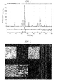
- the result is shown in FIG. 1 .
- the diffraction peak originated from ZnO and the diffraction peak originated from Zn 2 SnO 4 which is a composite oxide of SnO 2 and ZnO, are detected in the oxide sputtering target related to the present invention. It confirms that there were ZnO phase and Zn 2 SnO 4 phase.
- the backscattered electron image (CP) and the element distribution image, which shows composition distributions of each element, of the oxide sputtering target related to the present invention were observed with EPMA (field-emission electron probe).
- the obtained backscattered electron image and the element distribution image are shown in FIG. 2 .
- the element distribution images obtained by EPMA were obtained as colored images. However, each image shown in FIG. 2 is depicted after conversion to a black and white image. Thus, in terms of the gray scale in the black and white images, the lightly grey portion (relatively white part) indicates the portion including a particular element at a higher concentration.
- the oxide sputtering target related to the present invention is made of ZnO phase and Zn 2 SnO 4 phase, and Al is selectively dispersed in the ZnO phase.
- the raw material powders of: ZnO; SnO 2 ; and Al 2 O 3 were used.
- the texture of the target is made of ZnO phase and Zn 2 SnO 4 phase, and one or more of Al, Ga, and In are selectively dispersed in the ZnO phase.
- an oxide sputtering target produce by using the raw material powders of: ZnO; SnO 2 ; one or more of Al 2 O 3 , and Ga 2 O 3 , In 2 O 3 ; and one or more of GeO 2 and Cr 2 O 3 , the texture of the target is made of ZnO phase and Zn 2 SnO 4 phase.
- texture of the oxide sputtering target one or more of Al, Ga, and In; and one or more of Ge and Cr, are selectively dispersed in the ZnO phase.
- the present invention was made based on the findings described above, and has aspects shown below.
- the above-described oxide sputtering targets related to the present invention is the oxide with the component composition including: with respect to a total content amount of metal compositions, 0.15 at% or more of one or more of Al, Ga, and In as a total content amount; 7 at% or more of Sn; and the balance Zn and inevitable impurities, wherein a total content amount of Al, Ga, In, and Sn is 36 at% or less. Therefore, specific resistance during sputtering is low enabling the direct-current (DC) sputtering stably. Thus, the film deposited by using the oxide sputtering target has a less extent of variation of reflectance as an optical recording media and high storage stability. Moreover, the film has flexibility and breakage-resistance.
- the reason for setting the total content amount of one or more of Al, Ga, and In to 0.15 at% or more in the above-described oxide sputtering target is that if it was less that 0.15 at%, the direct-current (DC) sputtering would become unstable making it easier to cause breakage of the film. It is preferable that the total content amount of one or more ofAl, Ga, and In is set in the range of 0.20 at% or more and 6.0 at% or less.
- the reason for setting the content amount of Sn to 7 at% or more is that if it is less than 7 at%, the hardness of the film (indentation hardness which is explained later) would become 800mgf/ ⁇ m 2 or more and make the film harder.
- the content amount of Sn is set in the range of 7 at% or more and 30 at% or less.
- the reason for setting the total content amount of Al, Ga, In, and Sn to 36 at% or less is that if it exceeded 36 at%, tin oxide phase would reside within the texture of the sputtering target. The nodules are formed in the sputtering target due to the resided tin oxide phase, causing frequent occurrence of particle formation or abnormal electrical discharge during sputtering.
- an oxide sputtering target related present invention 1.0 to 20.0 at% of one or more of Ge and Cr as a total content amount is included.
- the reason for setting the total content amount of Cr and Ge to 20 at% or less is that if it exceeded 20 at%, the specific resistance of the target would become too high making it difficult to perform the direct-current (DC) sputtering stably.
- the specific resistance of the sputtering target is set to 1 ⁇ cm or less.
- the specific resistance of the sputtering target is set to 0.1 ⁇ cm or less. Even more preferably, it is set to 0.01 ⁇ cm or less.
- each of raw material powders of: ZnO; SnO 2 ; Al 2 O 3 ; Ga 2 O 3 ; In 2 O 3 ; GeO 2 ; and Cr 2 O 3 is prepared. Then, each of raw powders are weighted in order to obtain a component composition of the protective film for an optical recording media intended to be deposited.
- the weighted raw material powders and 3 times weight of zirconia balls were placed in a plastic container. Then, the contents in the plastic container were wet-mixed with a ball mill apparatus for 16 hours. During mixing, for example, alcohol was used as a solvent. Next, the obtained mixed powder was dried and granulated. Then, an oxide sintered body was obtained by performing the hot press (HP) process under a vacuum or an inert gas atmosphere under pressure of 150 to 400kgf/cm 2 for 2 to 9 hours at 850-1050°C, or preferably at 900-1000°C. Then, the obtained oxide sintered body is machine-worked into a predetermined shape to obtain an oxide sputtering target.
- HP hot press
- the protective film for an optical recording media which is deposited by using the oxide sputtering target produced as describe above, has the identical component composition to the oxide sputtering target.
- it includes: with respect to a total amount of metal compositions, 0.15 at% or more of one or more of Al, Ga, and In as a total amount; 7 at% or more of Sn; and the balance Zn and inevitable impurities, wherein a total amount of Al, Ga, In, and Sn is 36 at% or less.
- it includes: with respect to a total amount of metal compositions, 0.15 at% or more of one or more of Al, Ga, and In as a total amount; 7 at% or more of Sn; 1.0 to 20.0 at% of one or more of Ge and Cr as a total amount; and the balance Zn and inevitable impurities, wherein a total amount of Al, Ga, In, and Sn is 36 at% or less.
- the film has a less extent of variation of reflectance and high storage stability. Moreover, the film becomes appropriately flexible and resistant to breakage.
- the film is suitable for utilizing to the protective film of the multi-layered BD in which the recoding layer with an organic dye is used, for example.
- the oxide sputtering target is made of an oxide sintered body including: with respect to a total content amount of metal compositions, 0.15 at% or more of one or more of Al, Ga, and In as a total content amount; 7 at% or more of Sn; and the balance Zn and inevitable impurities, wherein a total content amount of Al, Ga, In, and Sn is 36 at% or less.
- an oxide sintered body including: with respect to a total content amount of metal compositions, 0.15 at% or more of one or more of Al, Ga, and In as a total content amount; 7 at% or more of Sn; 1.0 to 20.0 at% of one or more of Ge and Cr as a total content amount; and the balance Zn and inevitable impurities, wherein a total content amount of Al, Ga, In, and Sn is 36 at% or less.
- DC direct-current
- the protective film for an optical recording medium deposited by using the oxide sputtering target related to the present invention is suitable for utilizing to the dielectric material protective film of BD, which uses an organic dye as a recording layer.
- Embodiments of the oxide sputtering target and the protective film for an optical recording media, which are related to the present invention, are explained in detail below.
- the protective film for an optical recording media deposited by sputtering using the oxide sputtering target related to the present invention is an oxide an oxide including: with respect to a total content amount of metal compositions, 0.15 at% or more of one or more of Al, Ga, and In as a total content amount; 7 at% or more of Sn; and the balance Zn and inevitable impurities, wherein a total content amount of Al, Ga, In, and Sn is 36 at% or less.
- the protective film is made of an oxide including: with respect to a total content amount of metal compositions, 0.15 at% or more of one or more of Al, Ga, and In as a total content amount; 7 at% or more of Sn; 1.0 to 20.0 at% of one or more of Ge and Cr as a total content amount; and the balance Zn and inevitable impurities, wherein a total content amount ofAl, Ga, In, and Sn is 36 at% or less.
- the weighted raw material powders and 3 times weight of zirconia balls were placed in a plastic container. Then, the contents in the plastic container were wet-mixed with a ball mill apparatus for 16 hours to obtain the mixed powders of Examples 1-26 (Ex. 1-26). During mixing, alcohol was used as a solvent. Next, the obtained mixed powders of Examples 1-26 were dried and granulated. Then, each of the oxide sintered bodies were obtained by performing the hot press (HP) process under a vacuum under pressure of 350kgf/cm 2 for 3 hours at 950°C. Then, the obtained oxide sintered bodies were machine-worked to obtain the oxide sputtering targets of Examples 1-26. The target size was set to diameter of 125mm ⁇ thickness of 5mm.
- oxide sputtering targets related to the present invention were produced.
- the oxide sputtering target of Comparative Example 1 was produced by using the raw material powders of only Zn and SnO 2 , but without the raw material powders of Al 2 O 3 , Ga 2 O 3 , and In 2 O 3 . As in the cases including the raw material powders of Al 2 O 3 , Ga 2 O 3 , and In 2 O 3 , but their component composition ratios are out of the range configured in the present invention, the oxide sputtering targets of Comparative Examples 2 and 3 were produced.
- the oxide sputtering targets of Comparative Examples 4-6 were produced.
- the conventional sputtering targets of ZnS-SiO 2 (Comparative Example 7) and ITO (Comparative Example 8) were procured.
- ZnS-SiO 2 is the ZSSO target (20mol%SiO 2 ) manufactured by Mitsubishi Materials Corporation Ltd.
- ITO is the ITO target (10wt%SnO 2 ) manufactured by Mitsubishi Materials Corporation Ltd..
- the above-mentioned oxide sputtering target of Comparative Examples 1-8 (C. Ex. 1-8) were produced by following the identical production procedure to the oxide sputtering targets of Examples 1-26.
- the material composition (mol%) of each of the raw material powders related to the oxide sputtering targets of Comparative Examples 1-8 are shown in Table 1.
- Table 1 Raw Material Composition (mol%) Al 2 O 3 Ga 2 O 3 In 2 O 3 SnO 2 GeO 2 Cr 2 O 3 ZnO Ex. 1 0.1 - - 20 - - Balance Ex. 2 3 - - 30 - - Balance Ex. 3 3 - - 15 - - Balance Ex. 4 3 - - 20 - - Balance Ex.
- the oxide sputtering targets of Examples 1-26 and Comparative Examples 1-8; and the protective films for an optical recording media deposited by using these targets of Examples 1-26 and Comparative Examples 1-8 were evaluated.
- the oxide sputtering targets of Examples 1-26 and Comparative Examples 1-8 density ratio; specific resistance; the number of abnormal electrical discharges; and the amount of particles, were obtained.
- the protective films of Examples 1-26 and Comparative Examples 1-8 for an optical recording media indentation hardness; breakage of the film; XRD of the film; and variation of reflectance, were obtained. The ways to obtain these values are explained below.
- Density ratio was calculated by dividing the bulk density by the theoretical density after machine-working of the sintered bodies in a predetermined shape and measuring their weights to obtain the bulk density. The theoretical density was obtained based on the weights of raw materials as indicated below.
- ⁇ i ⁇ o 1 C 1 / 100 ⁇ 1 + C 2 / 100 ⁇ 2 + C 3 / 100 ⁇ 3 + C 4 / 100 ⁇ 4 + C 5 / 100 ⁇ 5 + C 6 / 100 ⁇ 6 + C 7 / 100 ⁇ 7 Unit : / cm 3 ⁇ 1 : Al 2 ⁇ O 3 density C 1 : Al 2 ⁇ O 3 wt % ⁇ 2 : Ga 2 ⁇ O 3 density C 2 : Ga 2 ⁇ O 3 wt % ⁇ 3 : ln 2 ⁇ O 3 density C 3 : ln 2 ⁇ O 3 wt % ⁇ 4 : ZnO density C 4 : ZnO wt % ⁇ 5 : Sn
- Films were deposited in the thickness of 100 nm on a PET film having thickness of 0.1 mm under deposition condition described above. After bending the film 10 times, the presence or absence of the breakage of the films was monitored by observing the surface of the film with a microscope (magnification rate: 1000-fold). When the deposition was made by radio frequency (RF) sputtering, it was labeled by a "*" mark.
- RF radio frequency
- Sample preparation Analysis samples were prepared by depositing films in 300nm of thickness on 1737 glass substrate manufactured by Corning Incorporated
- Sample preparation Analysis samples were prepared by wet-polishing targets with SiC-Paper (grit 180) and then by drying the polished targets.
- Presence or absence of SnO 2 phase was monitored by measuring the ratio of the peak near 27° corresponding to SnO 2 to the peak near 34° corresponding to Zn 2 SnO 4 .
- the indentation hardness showing flexibility (softness) of the protective film
- the indentation hardness exceeded 800mgf/ ⁇ m 2 in Comparative Examples 1 and 3.
- the indentation hardness was 800mgf/ ⁇ m 2 or less in the protective films of Examples 1-26, resulting in films with flexibility compared to Comparative Examples 1 and 3. Accordingly, there was no film breakage in the protective films of Examples 1-26.
- the protective film of Comparative Example 8 which was ITO film, film breakage occurred.
- the protective films of Examples 1-26 were in amorphous form in an ordinary temperature.
- X-ray diffraction (XRD) analysis was performed on each of the oxide sputtering targets of Examples 1-26.
- the diffraction peak originated from ZnO
- the diffraction peak originated from Zn 2 SnO 4 , which was a composite oxide of SnO 2 and ZnO, were detected.
- existence of ZnO phase and Zn 2 SnO 4 phase were confirmed.
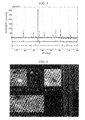
- FIG. 3 a graph showing results of X-ray diffraction (XRD) analysis of the oxide sputtering target of Comparative Example 2 is shown in FIG. 3 .
- EPMA field-emission electron probe
- CP backscattered electron image
- element distribution image showing composition distribution of each element were obtained and shown in FIG. 4 .
- the way to interpret the element distribution image obtained by EPMA is the same as in the case of FIG. 2 . Based on these images, it can be understood that: 1) the texture of the target was made of ZnO phase and Zn 2 SnO 4 phase, and Al was selectively dispersed in the ZnO phase in the element distribution image of the oxide sputtering target related to the present invention shown in FIG.
- ZnO 2 phase existed in the phase whose major component is ZnO in the oxide sputtering target of Comparative Example 2.
- the portion corresponding to the above-explained characteristics is indicated by the enclosure with a broken line in FIG. 4 . Presence of SnO 2 phase was also confirmed by the fact that the peak of SnO 2 in the XRD graph indicated 6/100.
- oxide sputtering targets it is preferable that: surface roughness being 5.0 ⁇ m or less, more preferably being 1.0 ⁇ m or less; the grain size being 20 ⁇ m or less, more preferably 10 ⁇ m or less; the concentration of metal-based impurities being 0.1 atomic% or less, more preferably 0.05 atomic % or less; and the flexural strength being 50MPa or more, more preferably 100MPa or more.
- the oxide sputtering targets of Examples 1-26 satisfied all the above-mentioned criteria.
- the pressure sintering was performed by the hot press procedure in Embodiments and Examples, the process can be done by the hot isostatic pressure type sintering method (HIP method) alternatively, for example.
- HIP method hot isostatic pressure type sintering method
- a protective film for an optical recording media which is suitable for utilization to the dielectric material protective film of BD which uses an organic dye as a recording layer, can be provided.
Landscapes
- Chemical & Material Sciences (AREA)
- Engineering & Computer Science (AREA)
- Ceramic Engineering (AREA)
- Manufacturing & Machinery (AREA)
- Materials Engineering (AREA)
- Organic Chemistry (AREA)
- Structural Engineering (AREA)
- Mechanical Engineering (AREA)
- Chemical Kinetics & Catalysis (AREA)
- Metallurgy (AREA)
- Inorganic Chemistry (AREA)
- Physics & Mathematics (AREA)
- Plasma & Fusion (AREA)
- Analytical Chemistry (AREA)
- Physical Vapour Deposition (AREA)
- Manufacturing Optical Record Carriers (AREA)
- Optical Record Carriers And Manufacture Thereof (AREA)
Abstract
The present invention relates to an oxide sputtering target. By using the oxide sputtering target for formation of a protective film for an optical recording medium, a film, which has high storage stability and breakage resistance due to flexibility, can be deposited. Also, it can be utilized for direct-current sputtering and forms a less amount of particles during sputtering. The oxide sputtering target is made of an oxide sintered body including: with respect to a total content amount of metal compositions, 0.15 at% or more of one or more of Al, Ga, and In as a total content amount; 7 at% or more of Sn; and the balance Zn and inevitable impurities, wherein a total content amount ofAl, Ga, In, and Sn is 36 at% or less.
Description
- The present invention relates to an oxide sputtering target for depositing a protective film for an optical recording medium, which is utilized for an optical recording medium such as CD, DVD, and Blu-ray Disc (registered trade mark: hereinafter referred as "BD"), and a protective film for an optical recording medium deposited by using the oxide sputtering target.
- Priority is claimed on Japanese Patent Application No.
2012-023397, filed February 6, 2012 2013-010035, filed January 23, 2013 - In recent years, sizes of digital data recorded on optical recording media have been increased with the availability of highly defined images and movies. Such trends strengthen the demand for a recording media with a higher capacity. As a high capacity optical recording media, BD which is capable of storing 50GB data by the multi-layer recoding method is already commercially available. In the above-mentioned BD, improvement of the currently available capacity is expected. Thus, research is conducted vigorously for obtaining even higher capacity by multi-stratifying the recoding layer.
-
- PTL 1: Japanese Unexamined Patent Application, First Publication No.
2009-26378 - PTL 2: Japanese Unexamined Patent Application, First Publication No.
2005-228402 - PTL 3: Japanese Unexamined Patent Application, First Publication No.
2005-154820 - The technology described above still has problems explained below.
- In a recording medium utilizing an organic dye for the recording layer, the recoding layer deforms in a larger extent compared to the recording layer utilizing an organic compound. Thus, the protective layer next to the dye has to have a lower hardness as described in Patent Literature 1 (PTL 1). Because of this, the film made of ZnS-SiO2 or ITO, which has suitable flexibility (softness), is utilized conventionally.
- However, when a sulfur (S) component is include as in ZnS-SiO2, the sulfur and the metal in the reflective coat react each other to reduce the reflectance as described in Patent Literature 2 (PTL 2). Thus, such films have a shortcoming of reduced storage stability as an optical recording medium. Also, in the case of using ITO, many particles are formed during sputtering to deteriorate the quality of the recording film of the recording media. In addition, the particle formation makes cleanup of the production facility cumbersome leading to a poor productivity of the recording media. In Patent Literature 3 (PTL 3), usage of a sputtering target whose major components are: tin oxide; zinc oxide; and an oxide of an element with valency of 3 or more, with tin oxide phase is proposed. However, usage of such a sputtering target causes a particle formation problem during sputtering due to nodulation of the tin oxide phase in the texture.
- The present invention is made under the circumstance described above. The purpose of the present invention is to provide an oxide sputtering target for formation of a protective film for an optical recording medium. By using the oxide sputtering target, a film, which has high storage stability, and breakage resistance due to flexibility, can be deposited. Also, it can be utilized for direct-current sputtering and forms a less amount of particles during sputtering.
- The inventors of the present invention conducted extensive study about ZnO-based sputtering target and found the followings. That is, by adding one or more of: zinc oxide (ZnO); tin oxide (SnO2); aluminum oxide (Al2O3); gallium oxide (Ga2O3); and indium oxide (In2O3) as the raw material of the sputtering target, a ZnO-based oxide sputtering target, by which a film with high storage stability and breakage resistance due to flexibility can be deposited, can be obtained by direct-current (DC) sputtering. Furthermore, in addition to the raw materials mentioned above, by adding one or more of germanium oxide (GeO2) and chromium oxide (Cr2O3), a ZnO-based oxide sputtering target, by which a film with high storage stability and breakage resistance due to flexibility can be deposited, can be obtained
- Thus, as an example of the present invention, a ZnO-based oxide sputtering target was produced. First, raw material powders of: zinc oxide (ZnO, D50=1 µm); tin oxide (SnO2, D50=10 µm); and aluminum oxide (Al2O3, D50=0.2 µm) were prepared. By using a ball mill apparatus, the raw material powders weighted to obtain a predetermined ratio of each powder were wet-mixed for 16 hours to obtain a mixed powder. Then, the mixed powder was dried and granulated. Then, the mixed powder was subjected to a hot press (HP) process under the pressure of 350kgf/cm2 for 3 hours at 950°C. The obtained oxide sintered body was machine-worked to be in a predetermined shape to produce the oxide sputtering target.
- Next, X-ray diffraction (XRD) analysis was performed on the produced oxide sputtering target. The result is shown in
FIG. 1 . As indicated in the result, the diffraction peak originated from ZnO and the diffraction peak originated from Zn2SnO4, which is a composite oxide of SnO2 and ZnO, are detected in the oxide sputtering target related to the present invention. It confirms that there were ZnO phase and Zn2SnO4 phase. - Also, the backscattered electron image (CP) and the element distribution image, which shows composition distributions of each element, of the oxide sputtering target related to the present invention were observed with EPMA (field-emission electron probe). The obtained backscattered electron image and the element distribution image are shown in
FIG. 2 . The element distribution images obtained by EPMA were obtained as colored images. However, each image shown inFIG. 2 is depicted after conversion to a black and white image. Thus, in terms of the gray scale in the black and white images, the lightly grey portion (relatively white part) indicates the portion including a particular element at a higher concentration. Based on the images presented, it is demonstrated that the oxide sputtering target related to the present invention is made of ZnO phase and Zn2SnO4 phase, and Al is selectively dispersed in the ZnO phase. - In the above-explained oxide sputtering target, the raw material powders of: ZnO; SnO2; and Al2O3 were used. In addition to the combination of the raw material powders explained above, it was found that in an oxide sputtering target produce by using the raw material powders of: ZnO; SnO2; and one or more of Al2O3, and Ga2O3, In2O3, the texture of the target is made of ZnO phase and Zn2SnO4 phase, and one or more of Al, Ga, and In are selectively dispersed in the ZnO phase. Furthermore, in addition to: ZnO; Sn02; and one or more of Al2O3, and Ga2O3, In2O3, it was found that in an oxide sputtering target produce by using the raw material powders of: ZnO; SnO2; one or more of Al2O3, and Ga2O3, In2O3; and one or more of GeO2 and Cr2O3, the texture of the target is made of ZnO phase and Zn2SnO4 phase. In texture of the oxide sputtering target: one or more of Al, Ga, and In; and one or more of Ge and Cr, are selectively dispersed in the ZnO phase.
- The present invention was made based on the findings described above, and has aspects shown below.
- (1) A oxide sputtering target made of an oxide sintered body including: with respect to a total content amount of metal compositions, 0.15 at% or more of one or more of Al, Ga, and In as a total content amount; 7 at% or more of Sn; and the balance Zn and inevitable impurities, wherein
a total content amount of Al, Ga, In, and Sn is 36 at% or less. - (2) A oxide sputtering target made of an oxide sintered body including: with respect to a total content amount of metal compositions, 0.15 at% or more of one or more of Al, Ga, and In as a total content amount; 7 at% or more of Sn; 1.0 to 20.0 at% of one or more of Ge and Cr as a total content amount; and the balance Zn and inevitable impurities, wherein
a total content amount of Al, Ga, In, and Sn is 36 at% or less. - (3) A protective film for an optical recording medium, which is deposited by sputtering using the oxide sputtering target according to (1) described above, wherein the protective film is an oxide with a component composition including: with respect to a total content amount of metal compositions, 0.15 at% or more of one or more of Al, Ga, and In as a total content amount; 7 at% or more of Sn; and the balance Zn and inevitable impurities, wherein a total content amount of Al, Ga, In, and Sn is 36 at% or less.
- (4) A protective film for an optical recording medium, which is deposited by sputtering using the oxide sputtering target according to (2) described above, wherein the protective film is an oxide with a component composition including: with respect to a total content amount of metal compositions, 0.15 at% or more of one or more of Al, Ga, and In as a total content amount; 7 at% or more of Sn; 1.0 to 20.0 at% of one or more of Ge and Cr as a total content amount; and the balance Zn and inevitable impurities, wherein a total content amount of Al, Ga, In, and Sn is 36 at% or less.
- The above-described oxide sputtering targets related to the present invention is the oxide with the component composition including: with respect to a total content amount of metal compositions, 0.15 at% or more of one or more of Al, Ga, and In as a total content amount; 7 at% or more of Sn; and the balance Zn and inevitable impurities, wherein a total content amount of Al, Ga, In, and Sn is 36 at% or less. Therefore, specific resistance during sputtering is low enabling the direct-current (DC) sputtering stably. Thus, the film deposited by using the oxide sputtering target has a less extent of variation of reflectance as an optical recording media and high storage stability. Moreover, the film has flexibility and breakage-resistance.
- In addition to the reduction of specific resistance of the sputtering target due to formation of carriers of Al, Ga, or In dissolved in ZnO, it is believed that thermal damage can be mitigated by improvement of thermal diffusivity of the deposited film
- The reason for setting the total content amount of one or more of Al, Ga, and In to 0.15 at% or more in the above-described oxide sputtering target is that if it was less that 0.15 at%, the direct-current (DC) sputtering would become unstable making it easier to cause breakage of the film. It is preferable that the total content amount of one or more ofAl, Ga, and In is set in the range of 0.20 at% or more and 6.0 at% or less. The reason for setting the content amount of Sn to 7 at% or more is that if it is less than 7 at%, the hardness of the film (indentation hardness which is explained later) would become 800mgf/µm2 or more and make the film harder. It is preferable that the content amount of Sn is set in the range of 7 at% or more and 30 at% or less. The reason for setting the total content amount of Al, Ga, In, and Sn to 36 at% or less is that if it exceeded 36 at%, tin oxide phase would reside within the texture of the sputtering target. The nodules are formed in the sputtering target due to the resided tin oxide phase, causing frequent occurrence of particle formation or abnormal electrical discharge during sputtering.
- Also, in an oxide sputtering target related present invention, 1.0 to 20.0 at% of one or more of Ge and Cr as a total content amount is included. The reason for setting the total content amount of Cr and Ge to 20 at% or less is that if it exceeded 20 at%, the specific resistance of the target would become too high making it difficult to perform the direct-current (DC) sputtering stably. In order to make it possible to perform the direct-current (DC) sputtering, it is preferable that the specific resistance of the sputtering target is set to 1Ω·cm or less. Particularly, in order to perform the direct-current (DC) sputtering stably, it is preferable that the specific resistance of the sputtering target is set to 0.1Ω·cm or less. Even more preferably, it is set to 0.01Ω·cm or less.
- Therefore, in producing of the oxide sputtering target related to the present invention, each of raw material powders of: ZnO; SnO2; Al2O3; Ga2O3; In2O3; GeO2; and Cr2O3, is prepared. Then, each of raw powders are weighted in order to obtain a component composition of the protective film for an optical recording media intended to be deposited.
- Then, the weighted raw material powders and 3 times weight of zirconia balls (diameter: 5 mm) were placed in a plastic container. Then, the contents in the plastic container were wet-mixed with a ball mill apparatus for 16 hours. During mixing, for example, alcohol was used as a solvent. Next, the obtained mixed powder was dried and granulated. Then, an oxide sintered body was obtained by performing the hot press (HP) process under a vacuum or an inert gas atmosphere under pressure of 150 to 400kgf/cm2 for 2 to 9 hours at 850-1050°C, or preferably at 900-1000°C. Then, the obtained oxide sintered body is machine-worked into a predetermined shape to obtain an oxide sputtering target.
- The protective film for an optical recording media, which is deposited by using the oxide sputtering target produced as describe above, has the identical component composition to the oxide sputtering target. Thus, it includes: with respect to a total amount of metal compositions, 0.15 at% or more of one or more of Al, Ga, and In as a total amount; 7 at% or more of Sn; and the balance Zn and inevitable impurities, wherein a total amount of Al, Ga, In, and Sn is 36 at% or less. Alternatively, it includes: with respect to a total amount of metal compositions, 0.15 at% or more of one or more of Al, Ga, and In as a total amount; 7 at% or more of Sn; 1.0 to 20.0 at% of one or more of Ge and Cr as a total amount; and the balance Zn and inevitable impurities, wherein a total amount of Al, Ga, In, and Sn is 36 at% or less.
- Therefore, the film has a less extent of variation of reflectance and high storage stability. Moreover, the film becomes appropriately flexible and resistant to breakage. Thus, the film is suitable for utilizing to the protective film of the multi-layered BD in which the recoding layer with an organic dye is used, for example.
- According to the oxide sputtering target related to the present invention, the oxide sputtering target is made of an oxide sintered body including: with respect to a total content amount of metal compositions, 0.15 at% or more of one or more of Al, Ga, and In as a total content amount; 7 at% or more of Sn; and the balance Zn and inevitable impurities, wherein a total content amount of Al, Ga, In, and Sn is 36 at% or less. Alternatively, it is made of an oxide sintered body including: with respect to a total content amount of metal compositions, 0.15 at% or more of one or more of Al, Ga, and In as a total content amount; 7 at% or more of Sn; 1.0 to 20.0 at% of one or more of Ge and Cr as a total content amount; and the balance Zn and inevitable impurities, wherein a total content amount of Al, Ga, In, and Sn is 36 at% or less. Because the configurations described above, it becomes possible to perform the direct-current (DC) sputtering stably. Moreover, a film, which has high storage stability and breakage resistance due to a suitable flexibility, can be deposited.
- Therefore, the protective film for an optical recording medium deposited by using the oxide sputtering target related to the present invention is suitable for utilizing to the dielectric material protective film of BD, which uses an organic dye as a recording layer.
-
-
FIG. 1 is a graph showing results of X-ray diffraction (XRD) analysis of the oxide sputtering target related to the present invention. -
FIG. 2 is an element distribution image on a cross-sectional texture of the oxide sputtering target related to the present invention. Each of elements are measured by EPMA. -
FIG. 3 is a graph showing results of X-ray diffraction (XRD) analysis of the oxide sputtering target related to a comparative example. -
FIG. 4 is an element distribution image on a cross-sectional texture of the oxide sputtering target related to a comparative example. Each of elements are measured by EPMA. - Embodiments of the oxide sputtering target and the protective film for an optical recording media, which are related to the present invention, are explained in detail below.
- The protective film for an optical recording media deposited by sputtering using the oxide sputtering target related to the present invention is an oxide an oxide including: with respect to a total content amount of metal compositions, 0.15 at% or more of one or more of Al, Ga, and In as a total content amount; 7 at% or more of Sn; and the balance Zn and inevitable impurities, wherein a total content amount of Al, Ga, In, and Sn is 36 at% or less. Alternatively, the protective film is made of an oxide including: with respect to a total content amount of metal compositions, 0.15 at% or more of one or more of Al, Ga, and In as a total content amount; 7 at% or more of Sn; 1.0 to 20.0 at% of one or more of Ge and Cr as a total content amount; and the balance Zn and inevitable impurities, wherein a total content amount ofAl, Ga, In, and Sn is 36 at% or less.
- Thus, in order to produce the oxide sputtering target, raw material powders of: zinc oxide (chemical formula: ZnO, D50=1 µm); tin oxide (chemical formula:SnO2, D50=16 µm); aluminum oxide (chemical formula: Al2O3, D50=0.2 µm); gallium oxide (chemical formula: Ga2O3, D50=1.7 µm); indium oxide (chemical formula: In2O3, D50=11 µm); germanium oxide (chemical formula: GeO2, D50=1.0 µm); and chromium oxide (chemical formula: Cr2O3, D50=0.4 µm), were prepared. Then, each of the raw material powders were selected and weighted in order to obtain the above-described component composition of the protective film for an optical recording media. Component compositions (mol%) of each of the raw material powders are shown in Table 1.
- Then, the weighted raw material powders and 3 times weight of zirconia balls (diameter: 5 mm) were placed in a plastic container. Then, the contents in the plastic container were wet-mixed with a ball mill apparatus for 16 hours to obtain the mixed powders of Examples 1-26 (Ex. 1-26). During mixing, alcohol was used as a solvent. Next, the obtained mixed powders of Examples 1-26 were dried and granulated. Then, each of the oxide sintered bodies were obtained by performing the hot press (HP) process under a vacuum under pressure of 350kgf/cm2 for 3 hours at 950°C. Then, the obtained oxide sintered bodies were machine-worked to obtain the oxide sputtering targets of Examples 1-26. The target size was set to diameter of 125mm×thickness of 5mm.
- Furthermore, for a comparison to the present embodiment of the oxide sputtering targets related to the present invention, oxide sputtering targets excluded from the scope of the present invention were produced.
- The oxide sputtering target of Comparative Example 1 was produced by using the raw material powders of only Zn and SnO2, but without the raw material powders of Al2O3, Ga2O3, and In2O3. As in the cases including the raw material powders of Al2O3, Ga2O3, and In2O3, but their component composition ratios are out of the range configured in the present invention, the oxide sputtering targets of Comparative Examples 2 and 3 were produced. Also, as in the cases including the raw material powders of Al2O3, Ga2O3, and In2O3 and further including at least one of GeO2 and Cr2O3, but their component composition ratios are out of the range configured in the present invention, the oxide sputtering targets of Comparative Examples 4-6 were produced. Also, the conventional sputtering targets of ZnS-SiO2 (Comparative Example 7) and ITO (Comparative Example 8) were procured. ZnS-SiO2 is the ZSSO target (20mol%SiO2) manufactured by Mitsubishi Materials Corporation Ltd.. ITO is the ITO target (10wt%SnO2) manufactured by Mitsubishi Materials Corporation Ltd.. The above-mentioned oxide sputtering target of Comparative Examples 1-8 (C. Ex. 1-8) were produced by following the identical production procedure to the oxide sputtering targets of Examples 1-26. The material composition (mol%) of each of the raw material powders related to the oxide sputtering targets of Comparative Examples 1-8 are shown in Table 1.
[Table 1] Raw Material Composition (mol%) Al2O3 Ga2O3 In2O3 SnO2 GeO2 Cr2O3 ZnO Ex. 1 0.1 - - 20 - - Balance Ex. 2 3 - - 30 - - Balance Ex. 3 3 - - 15 - - Balance Ex. 4 3 - - 20 - - Balance Ex. 5 3 - - 25 - - Balance Ex. 6 3 - - 8 - - Balance Ex. 7 - 0.1 - 20 - - Balance Ex. 8 - 3 - 20 - - Balance Ex. 9 - - 0.1 20 - - Balance Ex. 10 - - 3 20 - - Balance Ex. 11 1.5 1.5 - 20 - - Balance Ex. 12 1.5 - 1.5 20 - - Balance Ex. 13 - 1.5 1.5 20 - - Balance Ex. 14 1 1 1 20 - - Balance Ex. 15 3 - - 20 1 - Balance Ex. 16 3 - - 20 5 - Balance Ex. 17 3 - - 20 10 - Balance Ex. 18 3 - - 20 20 - Balance Ex. 19 3 - - 20 - 1 Balance Ex. 20 3 - - 20 - 5 Balance Ex. 21 3 - - 20 - 11 Balance Ex. 22 3 - - 20 5 5 Balance Ex. 23 - 3 - 20 10 - Balance Ex. 24 - 3 - 20 - 5 Balance Ex. 25 - - 3 20 10 - Balance Ex. 26 - - 3 20 - 5 Balance C. Ex. 1 - - - 20 - - Balance C. Ex. 2 3 - - 32 - - Balance C. Ex. 3 3 - - 6 - - Balance C. Ex. 4 3 - - 20 25 - Balance C. Ex. 5 3 - - 20 - 14 Balance C. Ex. 6 3 - - 20 12 6 Balance C. Ex. 7 (ZnS)80(SiO2)20mol% C. Ex. 8 ITO(10wt%SnO2) - Then, analysis of the metal composition was performed to the produced oxide sputtering targets of Examples 1-26 and Comparative Examples 1-8. Results of the analysis are shown in Table 2.
[Table 2] Target Composition (at% with respect to total metal compositions) Al Ga In Sn Al+Ga+In+Sn Ge+Cr ZnO Ex. 1 0.20 - - 20.0 20.20 - Balance Ex. 2 5.83 - - 29.1 34.93 - Balance Ex. 3 5.83 - - 14.6 20.43 - Balance Ex. 4 5.83 - - 19.4 25.23 - Balance Ex. 5 5.83 - - 24.3 30.13 - Balance Ex. 6 5.83 - - 7.8 13.63 - Balance Ex. 7 - 0.20 - 20.0 20.20 - Balance Ex. 8 - 5.83 - 19.4 25.23 - Balance Ex. 9 - - 0.20 20.0 20.20 - Balance Ex. 10 - - 5.83 19.4 25.23 - Balance Ex. 11 2.91 2.91 - 19.4 25.23 - Balance Ex. 12 2.91 - 2.91 19.4 25.23 - Balance Ex. 13 - 2.91 2.91 19.4 25.23 - Balance Ex. 14 1.94 1.94 1.94 19.4 25.23 - Balance Ex. 15 5.83 - - 19.4 25.23 1.0 Balance Ex. 16 5.83 - - 19.4 25.23 4.9 Balance Ex. 17 5.83 - - 19.4 25.23 9.7 Balance Ex. 18 5.83 - - 19.4 25.23 19.4 Balance Ex. 19 5.77 - - 19.2 24.97 1.0 Balance Ex. 20 5.56 - - 18.5 24.06 9.3 Balance Ex. 21 5.26 - - 17.5 22.76 19.3 Balance Ex. 22 5.56 - - 18.5 24.06 13.9 Balance Ex. 23 - 5.83 - 19.4 19.42 9.7 Balance Ex. 24 - 5.56 - 18.5 18.50 9.3 Balance Ex. 25 - - 5.83 19.4 19.42 9.7 Balance Ex. 26 - - 5.56 18.5 18.50 9.3 Balance C. Ex. 1 - - - 20.0 20.00 - Balance C. Ex. 2 5.83 - - 31.1 36.93 - Balance C. Ex. 3 5.83 - - 5.8 11.63 - Balance C. Ex. 4 5.83 - - 19.4 25.23 24.3 Balance C. Ex. 5 5.13 - - 17.1 22.23 23.9 Balance C. Ex. 6 5.50 - - 18.3 23.80 22.9 Balance C. Ex. 7 (ZnS)80(SiO2)20mol% C. Ex. 8 ITO(10wt%SnO2) - Next, by using the produced oxide sputtering targets of Examples 1-26 and Comparative Examples 1-8, the protective films for an optical recording media of Examples 1-26 and Comparative Examples 1-8 were deposited in the deposition conditions explained below.
-
- Power source: DC500W (partially radio frequency (RF) sputtering)
- Total pressure: Ar=47.5 sccm, O2=2.5 sccm (except for Comparative Example 7 in which Ar=50 sccm, O2=0 sccm)
- Distance between target and substrate (TS): 70 mm
- Then, analysis of the metal composition was performed to the protective films of Examples 1-26 and Comparative Examples 1-8 for an optical recording media, which were deposited by using the oxide sputtering targets of Examples 1-26 and Comparative Examples 1-8 under the deposition condition explained above. Results of the analysis are shown in Table 3. Based on the results, it was demonstrated that the metal compositions of the protective films of Examples 1-26 and Comparative Examples 1-8 for an optical recording media correspond to the metal compositions of the oxide sputtering targets of Examples 1-26 and Comparative Examples 1-8
[Table 3] Film Composition (at% with respect to total metal compositions) Al Ga In Sn Al+Ga+In+Sn Ge+Cr ZnO Ex. 1 0.20 - - 19.5 19.70 - Balance Ex. 2 5.86 - - 28.8 34.66 - Balance Ex. 3 5.88 - - 15.0 20.88 - Balance Ex. 4 5.79 - - 20.1 25.89 - Balance Ex. 5 5.80 - - 25.5 31.30 - Balance Ex. 6 5.82 - - 7.3 13.12 - Balance Ex. 7 - 0.18 - 21.0 21.18 - Balance Ex. 8 - 5.82 - 19.9 25.72 - Balance Ex. 9 - - 0.19 18.9 19.09 - Balance Ex. 10 - - 5.90 19.9 25.80 - Balance Ex. 11 2.90 2.88 - 18.9 24.68 - Balance Ex. 12 28.20 - 2.87 20.0 25.69 - Balance Ex. 13 - 2.93 2.99 18.7 24.62 - Balance Ex. 14 1.99 1.95 1.88 20.5 26.32 - Balance Ex. 15 5.83 - - 19.6 25.43 1.1 Balance Ex. 16 5.83 - - 19.4 25.24 5.0 Balance Ex. 17 5.83 - - 20.1 25.93 9.3 Balance Ex. 18 5.79 - - 18.8 24.59 19.5 Balance Ex. 19 5.67 - - 19.4 25.09 0.9 Balance Ex. 20 5.46 - - 19.2 24.66 4.3 Balance Ex. 21 5.22 - - 17.0 22.22 9.2 Balance Ex. 22 5.77 - - 19.2 24.97 9.1 Balance Ex. 23 - 5.78 - 19.6 25.38 9.3 Balance Ex. 24 - 5.38 - 19.7 25.08 9.8 Balance Ex. 25 - - 5.86 19.6 25.46 9.9 Balance Ex. 26 - - 5.49 20.0 25.49 8.9 Balance C. Ex. 1 - - - 20.2 20.00 - Balance C. Ex. 2 5.77 - - 30.5 36.27 - Balance C. Ex. 3 5.83 - - 6.0 11.83 - Balance C. Ex. 4 5.88 - - 18.9 24.78 23.8 Balance C. Ex. 5 5.08 - - 18.0 23.08 22.8 Balance C. Ex. 6 5.78 - - 19.5 25.28 22.9 Balance - Then, the oxide sputtering targets of Examples 1-26 and Comparative Examples 1-8; and the protective films for an optical recording media deposited by using these targets of Examples 1-26 and Comparative Examples 1-8 were evaluated. In regard to the oxide sputtering targets of Examples 1-26 and Comparative Examples 1-8: density ratio; specific resistance; the number of abnormal electrical discharges; and the amount of particles, were obtained. In regard to the protective films of Examples 1-26 and Comparative Examples 1-8 for an optical recording media: indentation hardness; breakage of the film; XRD of the film; and variation of reflectance, were obtained. The ways to obtain these values are explained below.
- Density ratio was calculated by dividing the bulk density by the theoretical density after machine-working of the sintered bodies in a predetermined shape and measuring their weights to obtain the bulk density. The theoretical density was obtained based on the weights of raw materials as indicated below.

- Specific resistance of the sputtering targets and films was measured by using the resistance measurement apparatus Loresta-GP manufacture by Mitsubishi Chemical Corporation Ltd..
- Under the condition described above, sputtering was performed for 12 hours and the number of abnormal discharges was counted. After sputtering, the sputter chamber was released, and the amount of the particles in the chamber was obtained.
- Alloy of Ag98.1Nd1.0Cu0.9 was sputtered on polycarbonate. Then, by using a substrate on which the dye described in Example 1 of PTL 1 was deposited, each protective film of Examples and Comparative Examples was deposited on it in the thickness of 14 nm under the condition described above. After that, they were allowed to stand for 100 hours at 80°C in a thermo-hygrostat set to 85% of humidity. Then, variation of reflectance was measured before and after the still standing. For the measurement of the reflectance, a UV-visible light spectrophotometer (Model V-550 manufacture by JASCO Corporation) was used. The reflectance was measured using the light with a wave length of 405 nm.
- By using 1737 glass manufactured by Corning Incorporated as a substrate, films with thickness of 500 nm were deposited under the above-described deposition condition. Then, indentation hardness was measured with a super-micro indentation tester (Model ENT-1100a manufactured by ELIONIX Corporation Ltd.) at the indentation load of 35mgf. First, the substrates were set in the apparatus at 27°C. Then, after 1 hour or longer has passed, the indentation hardness measurement was performed. The measured value was expressed as the average value of multiple raw data measured at 10 different points
- Films were deposited in the thickness of 100 nm on a PET film having thickness of 0.1 mm under deposition condition described above. After bending the
film 10 times, the presence or absence of the breakage of the films was monitored by observing the surface of the film with a microscope (magnification rate: 1000-fold). When the deposition was made by radio frequency (RF) sputtering, it was labeled by a "*" mark. - Sample preparation: Analysis samples were prepared by depositing films in 300nm of thickness on 1737 glass substrate manufactured by Corning Incorporated
- Apparatus: RINT-Ultima/PC manufacture by Rigaku Coropration
- Tube: Cu
- Tube voltage: 40 kV
- Tube current: 40 mA
- Scanning range (2θ): 50° to 80°
- Slit size: Divergence (DS) 2/3 degree, Scanning (SS) 2/3 degree, Reception of light (RS) 0.8 mm
- Width of measurement step: 0.02 degree in 2θ
- Scanning rate: 2 degree per minute
- Rotation speed of sample platform: 30 rpm
- When no peak was observed, it was indicated by a "○" mark. When a distinctive diffraction peak was observed, it was indicated by a "×" mark.
- Sample preparation: Analysis samples were prepared by wet-polishing targets with SiC-Paper (grit 180) and then by drying the polished targets.
- Presence or absence of SnO2 phase was monitored by measuring the ratio of the peak near 27° corresponding to SnO2 to the peak near 34° corresponding to Zn2SnO4.
- Evaluation results of: the oxide sputtering targets of Examples 1-26 and Comparative Examples 1-8; and the protective films of Examples 1-26 and Comparative Examples 1-8 deposited by using them, are shown in Tables 4 and 5.
[Table 4] Specific density (%) Specific resistance (Ω·cm) Number of abnormal discharges (times/hour) Amount of particles Ex. 1 92.8 5.8E-02 2 Low Ex. 2 92.6 9.0E-01 8 Low Ex. 3 92.4 1.3E-02 1 Low Ex. 4 95.8 6.6E-02 1 Low Ex. 5 96.7 1.2E-01 2 Low Ex. 6 95.5 8.7E-03 1 Low Ex. 7 94.5 3.4E-O2 0 Low Ex. 8 94.3 5.2E-02 0 Low Ex. 9 98.8 5.8E--02 1 Low Ex. 10 92.8 4.8E-02 0 Low Ex. 11 94.8 5.0E-02 0 Low Ex. 12 95.7 6.4E-02 3 Low Ex. 13 98.2 7.7E-02 2 Low Ex. 14 94.2 4.4E-02 1 Low Ex. 15 95.8 6.7E-02 4 Low Ex. 16 94.9 7.1E-02 4 Very low Ex. 17 98.2 9.2E-02 5 Very low Ex. 18 99.1 8.1E-01 15 Very low Ex. 19 95.6 6.6E-02 4 Low Ex. 20 97.6 8.1E-02 4 Very low Ex. 21 99.9 7.9E-02 6 Very low Ex. 22 95.8 9.9E-02 6 Very low Ex. 23 97.7 8.7E-02 5 Very low Ex. 24 97.6 9.1E-02 6 Very low Ex. 25 98.1 8.4E-02 7 Very low Ex. 26 93.5 8.3E-02 8 Very low C. Ex.1 95.5 8.2E+00 DC sputtering not possible Low C. Ex. 2 94.5 9.5E-01 89 High C. Ex. 3 93.7 1.1E-03 0 Low C. Ex. 4 93.4 9.5E+00 DC sputtering not possible Very low C. Ex. 5 92.8 1.1E+01 DC sputtering not possible Very low C. Ex. 6 95.4 1.0E+01 DC sputtering not possible Very low C. Ex. 7 99.9 Not in measurable range DC sputtering not possible Low C. Ex. 8 99.4 1.5E-04 15 High [Table 5] Indentation hardness (mgf/µm2) Film breakage Specific resistance of film (Ω·cm) XRD of film Variation of reflectance (%) @ 405 nm SnO2 peak Ex. 1 784 No 6.5E+02 ○ 0.4 ≤1/100 Ex. 2 700 No 2.3E+02 ○ 0.7 ≤1/100 Ex. 3 744 No 1.3E+03 ○ 0.7 ≤1/100 Ex. 4 767 No 4.2E+02 ○ 0.3 ≤1/100 Ex. 5 704 No 5.9E+02 ○ 0.9 ≤1/100 Ex. 6 795 No 1.4E+00 ○ 0.1 ≤1/100 Ex. 7 783 No 5.9E+02 ○ 0.4 ≤1/100 Ex. 8 777 No 4.9E+02 ○ 1.0 ≤1/100 Ex. 9 758 No 7.1E+02 ○ 0.6 ≤1/100 Ex. 10 743 No 5.1E+02 ○ 0.5 ≤1/100 Ex. 11 715 No 4.8E+02 ○ 0.7 ≤1/100 Ex. 12 754 No 6.6E+02 ○ 0.1 ≤1/100 Ex. 13 746 No 4.3E+02 ○ 0.6 ≤1/100 Ex. 14 734 No 5.4E+02 ○ 0.4 ≤1/100 Ex. 15 766 No 4.2E+02 ○ 0.5 ≤1/100 Ex. 16 745 No 3.2E+03 ○ 0.5 ≤1/100 Ex. 17 788 No Not in measurable range ○ 0.3 ≤1/100 Ex. 18 786 No Not in measurable range ○ 0.9 ≤1/100 Ex. 19 743 No 9.5E+02 ○ 0.8 ≤1/100 Ex. 20 758 No 2.3E+03 ○ 0.3 ≤1/100 Ex. 21 766 No Not in measurable range ○ 0.2 ≤1/100 Ex. 22 755 No Not in measurable range ○ 0.6 ≤1/100 Ex. 23 758 No Not in measurable range ○ 0.6 ≤1/100 Ex. 24 767 No Not in measurable range ○ 0.9 ≤1/100 Ex. 25 751 No Not in measurable range ○ 0.8 ≤1/100 Ex. 26 782 No Not in measurable range ○ 0.4 ≤1/100 C. Ex. 1 833 *Yes Not in measurable range ○ 0.5 ≤1/100 C. Ex. 2 690 No 1.9E+02 ○ 0.6 6/100 C. Ex. 3 834 Yes 1.5E-01 × 0.3 ≤1/100 C. Ex. 4 777 *No Not in measurable range ○ 0.5 <1/100 C. Ex. 5 797 *No Not in measurable range ○ 0.6 ≤1/100 C. Ex. 6 734 *No Not in measurable range ○ 0.2 <1/100 C. Ex. 7 568 *No Not in measurable range ○ -8.9 - C. Ex. 8 778 Yes 3.4E+01 ○ 0.2 - - As shown in the above-indicated evaluation results, specific resistance was 0.1Ω·cm or less in the oxide sputtering targets of Examples 1-26. At the same time, the number of abnormal discharges was extremely low and the amount of particles was less. Contrary to that, specific resistant was high, in a case higher than the upper limit of measureable range, in the oxide sputtering targets of Comparative Examples 1, 4, 5, 6, and 7, making it impossible to perform the direct-current (DC) sputtering. Thus, in regard to the oxide sputtering targets of Comparative Examples 1, 4, 5, 6, and 7, film deposition was performed by the radio frequency (RF) sputtering. In the oxide sputtering targets of Examples 1-26 and Comparative Examples 1-8, the specific density was 90% or more.
- Also, in regard to the indentation hardness showing flexibility (softness) of the protective film, the indentation hardness exceeded 800mgf/µm2 in Comparative Examples 1 and 3. In these protective films, breakage of film occurred. Contrary to that, the indentation hardness was 800mgf/µm2 or less in the protective films of Examples 1-26, resulting in films with flexibility compared to Comparative Examples 1 and 3. Accordingly, there was no film breakage in the protective films of Examples 1-26. In the protective film of Comparative Example 8, which was ITO film, film breakage occurred.
- Furthermore, in regard to variation of reflectance, there was only low variation rate, which was 1.0% or less, in the protective films of Examples 1-26 compared to Comparative Example 7 in which ZnS-SiO2 was used and there was high variation rate. In the protective films of Examples 1-26, high storage stability was obtained.
- The protective films of Examples 1-26 were in amorphous form in an ordinary temperature.
- Next, X-ray diffraction (XRD) analysis was performed on each of the oxide sputtering targets of Examples 1-26. In the analysis, the diffraction peak originated from ZnO and the diffraction peak originated from Zn2SnO4, which was a composite oxide of SnO2 and ZnO, were detected. Thus, existence of ZnO phase and Zn2SnO4 phase were confirmed.
- As references, a graph showing results of X-ray diffraction (XRD) analysis of the oxide sputtering target of Comparative Example 2 is shown in
FIG. 3 . Also, by EPMA (field-emission electron probe), a backscattered electron image (CP) and an element distribution image showing composition distribution of each element were obtained and shown inFIG. 4 . The way to interpret the element distribution image obtained by EPMA is the same as in the case ofFIG. 2 . Based on these images, it can be understood that: 1) the texture of the target was made of ZnO phase and Zn2SnO4 phase, and Al was selectively dispersed in the ZnO phase in the element distribution image of the oxide sputtering target related to the present invention shown inFIG. 2; and 2 ) ZnO2 phase existed in the phase whose major component is ZnO in the oxide sputtering target of Comparative Example 2. The portion corresponding to the above-explained characteristics is indicated by the enclosure with a broken line inFIG. 4 . Presence of SnO2 phase was also confirmed by the fact that the peak of SnO2 in the XRD graph indicated 6/100. - In order to utilize the present invention as the oxide sputtering targets, it is preferable that: surface roughness being 5.0 µm or less, more preferably being 1.0 µm or less; the grain size being 20 µm or less, more preferably 10 µm or less; the concentration of metal-based impurities being 0.1 atomic% or less, more preferably 0.05 atomic % or less; and the flexural strength being 50MPa or more, more preferably 100MPa or more. The oxide sputtering targets of Examples 1-26 satisfied all the above-mentioned criteria.
- The scope of the present invention is not particularly limited by the above-explained descriptions of Embodiments or Examples. Therefore, modifications can be made in the present invention within the scope of the present invention.
- For example, the pressure sintering was performed by the hot press procedure in Embodiments and Examples, the process can be done by the hot isostatic pressure type sintering method (HIP method) alternatively, for example.
- A protective film for an optical recording media, which is suitable for utilization to the dielectric material protective film of BD which uses an organic dye as a recording layer, can be provided.
Claims (4)
- A oxide sputtering target made of an oxide sintered body comprising: with respect to a total content amount of metal compositions, 0.15 at% or more of one or more of Al, Ga, and In as a total content amount; 7 at% or more of Sn; and the balance Zn and inevitable impurities, wherein
a total content amount ofAl, Ga, In, and Sn is 36 at% or less. - A oxide sputtering target made of an oxide sintered body comprising: with respect to a total content amount of metal compositions, 0.15 at% or more of one or more of Al, Ga, and In as a total content amount; 7 at% or more of Sn; 1.0 to 20.0 at% of one or more of Ge and Cr as a total content amount; and the balance Zn and inevitable impurities, wherein
a total content amount ofAl, Ga, In, and Sn is 36 at% or less. - A protective film for an optical recording medium, which is deposited by sputtering using the oxide sputtering target according to Claim 1, wherein the protective film is an oxide with a component composition comprising: with respect to a total content amount of metal compositions, 0.15 at% or more of one or more of Al, Ga, and In as a total content amount; 7 at% or more of Sn; and the balance Zn and inevitable impurities, wherein a total content amount of Al, Ga, In, and Sn is 36 at% or less.
- A protective film for an optical recording medium, which is deposited by sputtering using the oxide sputtering target according to Claim 2 , wherein the protective film is an oxide with a component composition comprising: with respect to a total content amount of metal compositions, 0.15 at% or more of one or more of Al, Ga, and In as a total content amount; 7 at% or more of Sn; 1.0 to 20.0 at% of one or more of Ge and Cr as a total content amount; and the balance Zn and inevitable impurities, wherein a total content amount of Al, Ga, In, and Sn is 36 at% or less.
Applications Claiming Priority (3)
| Application Number | Priority Date | Filing Date | Title |
|---|---|---|---|
| JP2012023397 | 2012-02-06 | ||
| JP2013010035A JP6212869B2 (en) | 2012-02-06 | 2013-01-23 | Oxide sputtering target |
| PCT/JP2013/052679 WO2013118748A1 (en) | 2012-02-06 | 2013-02-06 | Oxide sputtering target and protective film for optical recording medium |
Publications (1)
| Publication Number | Publication Date |
|---|---|
| EP2813598A1 true EP2813598A1 (en) | 2014-12-17 |
Family
ID=48947509
Family Applications (1)
| Application Number | Title | Priority Date | Filing Date |
|---|---|---|---|
| EP13746711.4A Withdrawn EP2813598A1 (en) | 2012-02-06 | 2013-02-06 | Oxide sputtering target and protective film for optical recording medium |
Country Status (7)
| Country | Link |
|---|---|
| US (1) | US9123360B2 (en) |
| EP (1) | EP2813598A1 (en) |
| JP (1) | JP6212869B2 (en) |
| KR (1) | KR20140128993A (en) |
| CN (1) | CN104136655A (en) |
| TW (2) | TWI570255B (en) |
| WO (1) | WO2013118748A1 (en) |
Families Citing this family (9)
| Publication number | Priority date | Publication date | Assignee | Title |
|---|---|---|---|---|
| JP5965338B2 (en) * | 2012-07-17 | 2016-08-03 | 出光興産株式会社 | Sputtering target, oxide semiconductor thin film, and manufacturing method thereof |
| TWI503435B (en) * | 2014-03-18 | 2015-10-11 | Solar Applied Mat Tech Corp | Cr2o3-zno compact sputtering target, method of preparing the same and its application |
| JP6041219B2 (en) * | 2014-08-27 | 2016-12-07 | 日立金属株式会社 | Sputtering target |
| JP6731147B2 (en) * | 2015-08-10 | 2020-07-29 | 日立金属株式会社 | Oxide sputtering target material |
| JP6319771B2 (en) * | 2015-11-06 | 2018-05-09 | 株式会社山王 | Porous nickel thin film and method for producing the same |
| JP6551683B2 (en) * | 2016-03-11 | 2019-07-31 | 住友金属鉱山株式会社 | Sn-Zn-O-based oxide sintered body and method for producing the same |
| KR102382130B1 (en) * | 2017-02-01 | 2022-04-01 | 이데미쓰 고산 가부시키가이샤 | Oxide semiconductor film, thin film transistor, oxide sintered body, and sputtering target |
| CN111448336B (en) * | 2017-12-28 | 2022-03-01 | 三井金属矿业株式会社 | Oxide sintered body, sputtering target and oxide thin film |
| WO2020241165A1 (en) * | 2019-05-24 | 2020-12-03 | ソニー株式会社 | Imaging element, laminated imaging element, solid-state imaging device, and inorganic oxide semiconductor material |
Family Cites Families (17)
| Publication number | Priority date | Publication date | Assignee | Title |
|---|---|---|---|---|
| JP2001207256A (en) * | 2000-01-27 | 2001-07-31 | Mitsubishi Materials Corp | Sputtering target for optical recording medium protective film formation without spatter cracking |
| JP4793773B2 (en) * | 2003-03-04 | 2011-10-12 | Jx日鉱日石金属株式会社 | Manufacturing method of sputtering target |
| US7635440B2 (en) * | 2003-03-04 | 2009-12-22 | Nippon Mining & Metals Co., Ltd. | Sputtering target, thin film for optical information recording medium and process for producing the same |
| TWI370449B (en) * | 2003-07-25 | 2012-08-11 | Panasonic Corp | Information recording medium and method for producing the same |
| JP4711244B2 (en) | 2003-11-25 | 2011-06-29 | Jx日鉱日石金属株式会社 | Sputtering target |
| JP2005228402A (en) | 2004-02-12 | 2005-08-25 | Fuji Photo Film Co Ltd | Optical recording medium |
| JP4761868B2 (en) | 2005-07-27 | 2011-08-31 | 出光興産株式会社 | Sputtering target, manufacturing method thereof and transparent conductive film |
| US8304359B2 (en) * | 2005-09-27 | 2012-11-06 | Idemitsu Kosan Co., Ltd. | Sputtering target, transparent conductive film, and transparent electrode for touch panel |
| US8110273B2 (en) * | 2005-12-02 | 2012-02-07 | Panasonic Corporation | Optical information recording medium, recording/reproducing method thereof and recording/reproducing apparatus |
| JP4552950B2 (en) * | 2006-03-15 | 2010-09-29 | 住友金属鉱山株式会社 | Oxide sintered body for target, manufacturing method thereof, manufacturing method of transparent conductive film using the same, and transparent conductive film obtained |
| JP2008097791A (en) * | 2006-09-11 | 2008-04-24 | Ricoh Co Ltd | Multilayer phase change optical recording medium |
| JP5244331B2 (en) * | 2007-03-26 | 2013-07-24 | 出光興産株式会社 | Amorphous oxide semiconductor thin film, manufacturing method thereof, thin film transistor manufacturing method, field effect transistor, light emitting device, display device, and sputtering target |
| JP2009026378A (en) | 2007-07-19 | 2009-02-05 | Mitsubishi Kagaku Media Co Ltd | Optical recording medium |
| JP5269501B2 (en) * | 2008-07-08 | 2013-08-21 | 出光興産株式会社 | Oxide sintered body and sputtering target comprising the same |
| JP5307144B2 (en) * | 2008-08-27 | 2013-10-02 | 出光興産株式会社 | Field effect transistor, manufacturing method thereof, and sputtering target |
| JP2010120803A (en) * | 2008-11-19 | 2010-06-03 | Tosoh Corp | Multiple oxide sintered compact |
| JP5440388B2 (en) * | 2010-05-26 | 2014-03-12 | 三菱マテリアル株式会社 | Oxide sputtering target and oxide film for optical recording medium |
-
2013
- 2013-01-23 JP JP2013010035A patent/JP6212869B2/en not_active Expired - Fee Related
- 2013-02-06 WO PCT/JP2013/052679 patent/WO2013118748A1/en not_active Ceased
- 2013-02-06 EP EP13746711.4A patent/EP2813598A1/en not_active Withdrawn
- 2013-02-06 US US14/375,319 patent/US9123360B2/en not_active Expired - Fee Related
- 2013-02-06 TW TW102104560A patent/TWI570255B/en not_active IP Right Cessation
- 2013-02-06 CN CN201380008362.9A patent/CN104136655A/en active Pending
- 2013-02-06 KR KR20147021902A patent/KR20140128993A/en not_active Withdrawn
- 2013-02-06 TW TW105137667A patent/TWI605140B/en not_active IP Right Cessation
Non-Patent Citations (1)
| Title |
|---|
| See references of WO2013118748A1 * |
Also Published As
| Publication number | Publication date |
|---|---|
| TW201716604A (en) | 2017-05-16 |
| US9123360B2 (en) | 2015-09-01 |
| US20150010727A1 (en) | 2015-01-08 |
| TW201348481A (en) | 2013-12-01 |
| KR20140128993A (en) | 2014-11-06 |
| WO2013118748A1 (en) | 2013-08-15 |
| TWI570255B (en) | 2017-02-11 |
| CN104136655A (en) | 2014-11-05 |
| JP6212869B2 (en) | 2017-10-18 |
| JP2013177676A (en) | 2013-09-09 |
| TWI605140B (en) | 2017-11-11 |
Similar Documents
| Publication | Publication Date | Title |
|---|---|---|
| US9123360B2 (en) | Oxide sputtering target and protective film for optical recording medium | |
| CN102959122A (en) | Method for producing sputtering target, and sputtering target | |
| JP6042520B1 (en) | Mn—Zn—O-based sputtering target and method for producing the same | |
| CN105986230A (en) | Oxide sintered compact, sputtering target, thin film and method of producing oxide sintered compact | |
| JP6501008B2 (en) | Oxide sputtering target and method of manufacturing the same | |
| WO2016121367A1 (en) | Mn-Zn-W-O SPUTTERING TARGET AND MANUFACTURING METHOD THEREFOR | |
| EP3210952B1 (en) | Oxide sintered compact, oxide sputtering target, and oxide thin film | |
| TWI788351B (en) | Mn-W-Cu-O-BASED SPUTTERING TARGET AND METHOD FOR MANUFACTURING THE SAME | |
| KR101583124B1 (en) | Sintered compact of conductive oxide and method for manufacturing the same | |
| JP5440388B2 (en) | Oxide sputtering target and oxide film for optical recording medium | |
| JP5896121B2 (en) | Oxide sputtering target and protective film for optical recording medium | |
| TW201816158A (en) | Mn-Zn-O based sputtering target and production method thereror | |
| TWI554626B (en) | Oxide sputtering target and protective film for optical recording medium | |
| JP2013144820A (en) | Oxide sputtering target and protective film for optical recording medium | |
| JP2012224903A (en) | Oxide sputtering target, and method for manufacturing the same | |
| JP2013237893A (en) | Oxide sputtering target and protective film for optical recording medium |
Legal Events
| Date | Code | Title | Description |
|---|---|---|---|
| PUAI | Public reference made under article 153(3) epc to a published international application that has entered the european phase |
Free format text: ORIGINAL CODE: 0009012 |
|
| 17P | Request for examination filed |
Effective date: 20140804 |
|
| AK | Designated contracting states |
Kind code of ref document: A1 Designated state(s): AL AT BE BG CH CY CZ DE DK EE ES FI FR GB GR HR HU IE IS IT LI LT LU LV MC MK MT NL NO PL PT RO RS SE SI SK SM TR |
|
| AX | Request for extension of the european patent |
Extension state: BA ME |
|
| DAX | Request for extension of the european patent (deleted) | ||
| STAA | Information on the status of an ep patent application or granted ep patent |
Free format text: STATUS: THE APPLICATION HAS BEEN WITHDRAWN |
|
| 18W | Application withdrawn |
Effective date: 20151028 |