EP2811703A1 - Demodulation device, demodulation method, and program - Google Patents
Demodulation device, demodulation method, and program Download PDFInfo
- Publication number
- EP2811703A1 EP2811703A1 EP13743565.7A EP13743565A EP2811703A1 EP 2811703 A1 EP2811703 A1 EP 2811703A1 EP 13743565 A EP13743565 A EP 13743565A EP 2811703 A1 EP2811703 A1 EP 2811703A1
- Authority
- EP
- European Patent Office
- Prior art keywords
- channel
- input signal
- unit
- signal
- frequency
- Prior art date
- Legal status (The legal status is an assumption and is not a legal conclusion. Google has not performed a legal analysis and makes no representation as to the accuracy of the status listed.)
- Granted
Links
- 238000000034 method Methods 0.000 title claims abstract description 122
- 238000001514 detection method Methods 0.000 claims abstract description 128
- 238000012937 correction Methods 0.000 claims abstract description 60
- 238000011143 downstream manufacturing Methods 0.000 claims description 4
- 238000010586 diagram Methods 0.000 description 9
- 230000005540 biological transmission Effects 0.000 description 7
- 230000006870 function Effects 0.000 description 4
- 238000013507 mapping Methods 0.000 description 4
- 238000004891 communication Methods 0.000 description 3
- 230000001360 synchronised effect Effects 0.000 description 3
- 230000007423 decrease Effects 0.000 description 2
- 230000003111 delayed effect Effects 0.000 description 2
- 230000000694 effects Effects 0.000 description 2
- 230000010363 phase shift Effects 0.000 description 2
- 238000011144 upstream manufacturing Methods 0.000 description 2
- 238000005516 engineering process Methods 0.000 description 1
- 238000001914 filtration Methods 0.000 description 1
- 238000012986 modification Methods 0.000 description 1
- 230000004048 modification Effects 0.000 description 1
- 230000003287 optical effect Effects 0.000 description 1
- 238000012545 processing Methods 0.000 description 1
- 239000004065 semiconductor Substances 0.000 description 1
Images


Classifications
-
- H—ELECTRICITY
- H03—ELECTRONIC CIRCUITRY
- H03D—DEMODULATION OR TRANSFERENCE OF MODULATION FROM ONE CARRIER TO ANOTHER
- H03D3/00—Demodulation of angle-, frequency- or phase- modulated oscillations
- H03D3/007—Demodulation of angle-, frequency- or phase- modulated oscillations by converting the oscillations into two quadrature related signals
-
- H—ELECTRICITY
- H04—ELECTRIC COMMUNICATION TECHNIQUE
- H04L—TRANSMISSION OF DIGITAL INFORMATION, e.g. TELEGRAPHIC COMMUNICATION
- H04L27/00—Modulated-carrier systems
- H04L27/18—Phase-modulated carrier systems, i.e. using phase-shift keying
- H04L27/22—Demodulator circuits; Receiver circuits
-
- H—ELECTRICITY
- H04—ELECTRIC COMMUNICATION TECHNIQUE
- H04L—TRANSMISSION OF DIGITAL INFORMATION, e.g. TELEGRAPHIC COMMUNICATION
- H04L1/00—Arrangements for detecting or preventing errors in the information received
- H04L1/004—Arrangements for detecting or preventing errors in the information received by using forward error control
- H04L1/0045—Arrangements at the receiver end
- H04L1/0047—Decoding adapted to other signal detection operation
-
- H—ELECTRICITY
- H04—ELECTRIC COMMUNICATION TECHNIQUE
- H04L—TRANSMISSION OF DIGITAL INFORMATION, e.g. TELEGRAPHIC COMMUNICATION
- H04L27/00—Modulated-carrier systems
- H04L27/32—Carrier systems characterised by combinations of two or more of the types covered by groups H04L27/02, H04L27/10, H04L27/18 or H04L27/26
- H04L27/34—Amplitude- and phase-modulated carrier systems, e.g. quadrature-amplitude modulated carrier systems
- H04L27/38—Demodulator circuits; Receiver circuits
-
- H—ELECTRICITY
- H03—ELECTRONIC CIRCUITRY
- H03D—DEMODULATION OR TRANSFERENCE OF MODULATION FROM ONE CARRIER TO ANOTHER
- H03D2200/00—Indexing scheme relating to details of demodulation or transference of modulation from one carrier to another covered by H03D
- H03D2200/0041—Functional aspects of demodulators
- H03D2200/005—Analog to digital conversion
-
- H—ELECTRICITY
- H04—ELECTRIC COMMUNICATION TECHNIQUE
- H04L—TRANSMISSION OF DIGITAL INFORMATION, e.g. TELEGRAPHIC COMMUNICATION
- H04L27/00—Modulated-carrier systems
- H04L27/0014—Carrier regulation
- H04L2027/0044—Control loops for carrier regulation
- H04L2027/0063—Elements of loops
- H04L2027/0065—Frequency error detectors
Definitions
- the present technique relates to a demodulation device, a demodulation method and a program, and in particular, relates to a demodulation device, a demodulation method and a program capable of realizing a demodulation process at a rate equivalent to a case where an I channel and a Q channel are not inverted, even when the I channel and the Q channel are inverted.
- a tuner that receives a digitally modulated signal inputs a signal to a demodulation device that demodulates a digitally modulated signal, and an I channel (in-phase component) and a Q channel (quadrature component) of the input signal may be inverted, preventing normal demodulation of the input signal as it is.
- Patent Literature 2 switches the channels (also referred to as inversion control) and reprocesses all from the beginning after detecting the channel inversion, in order to perform demodulation process. Therefore, due to the need to reestablish the synchronization of the frequency and clock each time the channels are switched, demodulation process time sometimes becomes longer when the inversion of the channels has occurred than when there is no inversion of the channels.
- the present technique has been devised in view of the above circumstances, and is intended, in particular when channels are inverted, to realize a demodulation process at a rate equivalent to a case where channels are not inverted, even when channels are inverted, through performing the inversion control to the downstream process which is the clock synchronization or the frequency synchronization.
- a demodulation device that demodulates an input signal split into two signals of an I channel and a Q channel, the demodulation device including a frequency correction unit that corrects a frequency of the input signal and synchronizes the frequency, an inversion detection unit that detects the I channel and the Q channel of the input signal are inverted, and a channel control unit that switches, if it is detected that the I channel and the Q channel are inverted by the inversion detection unit, the I channel and the Q channel at a downstream of the frequency correction unit.
- the channel control unit may switch channels of the input signal at timing from which a frame of the input signal changes.
- the channel control unit may again switch channels of the input signal, if frame synchronization to the input signal is not established within a predetermined time period after switching channels of the input signal.
- a demodulation method of a demodulation device that demodulates an input signal split into two signals of an I channel and a Q channel
- the demodulation method including the steps of executing a frequency correction process that corrects frequency of the input signal and synchronizes the frequency, executing an inversion detection process that detects the I channel and the Q channel of the input signal are inverted, and executing a channel control process that switches, if it is detected that the I channel and the Q channel are inverted in the inversion detection process, the I channel and the Q channel in a downstream process of the frequency correction process.
- a program for causing a computer controlling a demodulation device that demodulates an input signal split into two signals of an I channel and a Q channel, to function as a frequency correction unit that corrects a frequency of the input signal and synchronizes the frequency, an inversion detection unit that detects the I channel and the Q channel of the input signal are inverted, and a channel control unit that switches, if it is detected that the I channel and the Q channel are inverted by the inversion detection unit, the I channel and the Q channel at a downstream of the frequency correction unit.
- a frequency correction unit that corrects the frequency of an input signal and synchronizes the frequency, and inversion of the I channel and the Q channel being the input signal is detected.
- the inversion of the I channel and the Q channel is detected, in a process subsequent to a configuration for establishing synchronization by frequency correction, the I channel and the Q channel are switched.
- a demodulation device of the present technique may be an independent device, or may be a block that performs a demodulation process.
- the I channel signal and the Q channel signal are input under an inverted state, it is possible to realize a demodulation process at a rate equivalent to that in a non-inverted state.
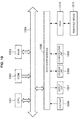
- FIG. 1 is a block diagram illustrating an embodiment of a receiving system including a demodulation device according to the present technique.
- the reception system of FIG 1 is a system for receiving and demodulating a broadcast signal that are in conformity with DVB-S.2 standard (hereinafter also referred to as input signal).
- the DVB-S.2 standard is a standard above DVB-S standard standardized by ETSI (European Telecommunications Standards Institute) for general use.
- the DVB-S.2 standard seeks to improve efficiency of frequency utilization and to improve C/N ratio (Carrier to Noise ratio) per frequency unit, through introducing multiple phase shift keying or LDPC (Low Density Parity Check) code.
- LDPC Low Density Parity Check
- synchronization pilot signal or PL (physical layer) header for transmitting the transmission information on a physical layer has been introduced as a standard, in order to ensure synchronization performance at low C/N ratio.
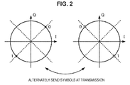
- FIG. 2 is a view showing a mapping pattern for each symbol in the ⁇ /2 shift BPSK on a complex plane. A mapping pattern of odd numbered symbols is shown on the left side of FIG. 2 , and a mapping pattern of even numbered symbols is shown on the right side thereof.
- the odd numbered symbols are mapped in such a manner that the argument is ⁇ /4 when the value is zero, and the argument is 5 ⁇ /4 when the value is one, and the even numbered symbols are mapped in such a manner that, the argument is 3 ⁇ /4 when the value is zero, and the argument is 7 ⁇ /4 when the value is one. Therefore, the phase difference between the adjacent symbols is limited to ⁇ /2.
- the receiving system is configured to include an antenna 11, a tuner 12, A/D converters 13-1, 13-2, and a demodulation device 14.
- the tuner 12 receives an input signal conforming to the DVB-S.2 standard via the antenna 11, separates the received input signal into two signals of I channel and Q channel, and supplies the separated signals to the A/D converters 13-1, 13-2, respectively.
- a signal of the I channel is also referred to as an I channel signal
- a signal of the Q channel is also referred to as a Q channel signal.
- the A/D converters 13-1 and 13-2 convert the I channel signal or the Q channel signal being an input signal from an analog signal into a digital signal, and supplies the converted signal to a frequency correction unit 31 of the demodulation device 14.
- the demodulation device 14 is structured to include a frequency correction unit 31, a frequency synchronization unit 32, a clock synchronization unit 33, a reception filter 34, a channel inversion control unit 35, an equalizer 36, a frame synchronization unit 37, a phase synchronization unit 38, and an error correction unit 39.
- the frequency correction unit 31 corrects the frequency of the input signal, and supplies the corrected input signal to the clock synchronization unit 33.
- the clock synchronization unit 33 synchronizes, with the clock signal, the input signal whose frequency is corrected by the frequency correction unit 31, supplies the synchronized input signal to the frequency synchronization unit 32 and the reception filter 34.
- the frequency synchronization unit 32 obtains a correction amount that is required to synchronize the frequency of the input signal with a predetermined frequency, and supplies the frequency correction unit 31 with the obtained correction amount as a correction signal.
- synchronization of the clock and the frequency of the input signal is established by a loop of the frequency correction unit 31, the frequency synchronization unit 32 and the clock synchronization unit 33.
- the reception filter 34 is, for example, a roll-off filter, and provides the channel inversion control unit 35 with the result of the filtering.
- the channel inversion control unit 35 switches and outputs the I channel signal and the Q channel signal being the input signal supplied from the reception filter 34. Further, if it is necessary to switch the I channel signal and the Q channel signal according to the channel inversion detection result, the channel inversion control unit 35 switches the I channel signal and the Q channel signal, at the timing of obtaining a frame start signal supplied from a frame synchronization determination unit 53 of the frame synchronization unit 37, and supplies the switched I channel signal and the Q channel signal to the equalizer 36.
- the equalizer 36 restores each component degraded on the transmission path associated with the transmission with regard to the I channel signal and the Q channel signal supplied from the channel inversion control unit 35, and supplies the restored I channel signal and Q channel signal to the frame synchronization unit 37.
- the frame synchronization unit 37 performs synchronization control to the input signal per frame unit.
- the frame synchronization unit 37 supplies the phase synchronization unit 38 with the input signal supplied from the equalizer 36 as it is.
- the frame synchronization unit 37 includes the channel inversion detection unit 51, a correlation detection unit 52, and the frame synchronization determination unit 53, and performs channel control along with the synchronization control.
- the channel inversion detection unit 51 detects whether or not the phases of I channel and Q channel of the signal to be output to the phase synchronization unit 38 are in a right relation, i.e., the phase of Q channel is delayed by ⁇ /2 with respect to the phase of I channel. More specifically, the channel inversion detection unit 51 detects whether or not the relation of the phases of the I and Q channels are correct according to the correlation value from the correlation detection unit 52, the determination result of the reliability of the correlation value, a synchronization state of the frame notified from the frame synchronization determination unit 53, or the state of the decoding synchronization by the error correction process which is notified from the error correction unit 39.
- the channel inversion detection unit 51 supplies the channel inversion control unit 35 with the detection result as the channel inversion detection result. Based on the channel inversion detection result, when the phase relation is not correct and needs switching, the channel inversion control unit 35 switches the channels of the input signal.
- switching the channels of the input signal means that reversing the phase relation of the I channel signal and the Q channel signal input to the channel inversion control unit 35 from the reception filter 34.
- methods of switching the channels of the input signal includes a method such as switching, by a selector, the signal output from each output terminal, and a method of reversing, by an inverter, the phases by inverting the polarity of one of the signals output from each output terminal.
- the correlation detection unit 52 performs delay detection to the complex symbol sequence of the input signal (hereinafter, also referred to as a received sequence), through performing complex multiplication of the complex conjugate of the symbol preceding the current symbol and the current symbol.
- the correlation detection unit 52 correlates a symbol sequence of the received delay detection value
- a received delay detection sequence a symbol sequence (hereinafter, also referred to as a known delay detection sequence) of a correct delay detection value (hereinafter, also referred to as a known delay detection value) of a symbol sequence of a known value (hereinafter, also referred to as a known sequence) that is periodically inserted in the input signal, such as a portion of the PL header or a synchronization pilot signal, and supplies the resulting correlation value to the channel inversion detection unit 51 and the frame synchronization determination unit 53.
- the correlation detection unit 52 determines the reliability of the correlation value, and notifies the channel inversion detection unit 51 of the determination result.
- the correlation detection unit 52 calculates, regarding a sequence SOF (Start Of Frame) in PL header inserted at the beginning of each header in the input signal as a known sequence, the correlation value between the known delay detection sequence corresponding to the known sequence and the received delay detection sequence.
- SOF Start Of Frame
- the frame synchronization determination unit 53 detects a peak value of the correlation value appearing in a frame period and the timing thereof (hereinafter, also referred to as peak timing).
- the frame synchronization determination unit 53 synchronizes the input signal for a frame unit according to a peak value and peak timing of the detected correlation value.
- the frame synchronization determination unit 53 supplies a frame synchronization status, and a signal indicating the peak timing of the correlation value to the channel inversion detection unit 51. Further, the frame synchronization determination unit 53 supplies the phase synchronization unit 38 with a frame synchronization status and a signal indicating, for example, the top position of each frame of the input signal. Furthermore, the frame synchronization determination unit 53 supplies the channel inversion control unit 35, as a frame start signal, information of the top position of each frame.
- the phase synchronization unit 38 corrects the phase error of each symbol of the input signal, and supplies the corrected signal to the error correction unit 39.
- the error correction unit 39 applies, to the input signal, LDPC or BCH decoding, or error correction (FEC (Forward Error Correction)), etc. such as Viterbi decoding, Reed-Solomon decoding, etc., and TS (Transport stream) packets obtained as a result is output to a downstream device. Further, the error correction unit 39 supplies the channel inversion detection unit 51 of the frame synchronization unit 37 with a signal indicating the decoding synchronization status resulting from an error correction and decoding process.
- FEC Forward Error Correction
- step S1 the tuner 12 receives an input signal in conformity with the DVB-S.2 standard via the antenna 11, splits the received input signal into two signals of I and Q channels, and supplies the A/D converters 13-1 and 13-2 therewith.
- step S2 the A/D converters 13-1 and 13-2 convert the input I channel signal or Q channel signal from an analog signal into a digital signal, and supply the converted signals to the frequency correction unit 31 of the demodulation device 14.
- step S3 the frequency correction unit 31 corrects the frequency of the input I channel and Q channel signal converted into a digital signal, according to the correction signal indicating the correction amount supplied from the frequency synchronization unit 32, and supplies the I channel signal and the Q channel signal to the clock synchronization unit 33.
- step S4 the clock synchronization unit 33 synchronizes, with a predetermined clock signal, the I channel signal and the Q channel signal converted into a digital signal, corrected with regards to the frequency thereof, and supplied from the frequency correction unit 31, and supplies the I channel signal and the Q channel signal to the frequency synchronization unit 32 and the reception filter 34.
- step S5 the frequency synchronization unit 32 generates a signal indicating a correction amount of the frequency of the I channel signal and the Q channel signal synchronized to the clock, and supplies the signal to the frequency correction unit 31.
- the same process is repeated by a loop constituted by the frequency correction unit 31, the frequency synchronization unit 32 and the clock synchronization unit 33, so that the frequency and clock synchronization is established.
- the established condition is continued.
- the reception filter 34 applies, for example, a roll-off filter to the I channel signal and the Q channel signal with synchronized frequency and clock, which are supplied from the clock synchronization unit 33, and supplies the I channel signal and the Q channel signal to the channel inversion control unit 35.
- a roll-off filter to the I channel signal and the Q channel signal with synchronized frequency and clock, which are supplied from the clock synchronization unit 33, and supplies the I channel signal and the Q channel signal to the channel inversion control unit 35.
- step S7 the channel inversion control unit 35 determines whether or not there has been supplied a channel inversion detection result indicating that the I channel signal and the Q channel signal are inverted by the channel inversion detection unit 51 of the frame synchronization unit 37.
- step S8 for example, if the process of steps S63 and S68 in FIG 6 described below has supplied, from the channel inversion detection unit 51, the channel inversion detection result indicating that the I channel signal and the Q channel signal are inverted, the process proceeds to step S8.
- step S8 the channel inversion control unit 35 determines whether or not a frame start signal has been supplied from the frame synchronization determination unit 53, and repeats the same process until the frame start signal is transmitted. Then, in step S8, when a frame start signal is supplied thereto by the processes of, for example, steps S65, S70 of FIG 6 described below, the process proceeds to step S9.
- step S9 the channel inversion control unit 35 inverts the I channel signal and the Q channel signal supplied from the reception filter 34 and supplies the inverted I channel signal and Q channel signal to the equalizer 36.
- step S7 if there has not been supplied a channel inversion detection result indicating that the I channel signal and the Q channel signal are inverted, from the channel inversion detection unit 51 of the frame synchronization unit 37, the process proceeds to step S10.
- step S10 the channel inversion control unit 35 supplies, to the equalizer 36, the I channel signal and the Q channel signal supplied from the reception filter 34 as they are without inverting.
- step S11 the equalizer 36 restores components degraded on the transmission path associated with the transmission, respectively, of the I channel signal and the Q channel signal supplied from the channel inversion control unit 35, and supplies the restored I channel signal and Q channel signal to the frame synchronization unit 37.
- step S12 the frame synchronization unit 37 executes the frame synchronization process, synchronizes the input signal frame by frame, and supplies, to the phase synchronization unit 38, the input signal supplied from the equalizer 36 as it is.
- step S21 the correlation detection unit 52 performs delay detection.
- the correlation detection unit 52 performs delay detection by performing a complex multiplication of the complex conjugate of the current symbol and the delayed symbol which is one symbol before the current symbol to the input signal, and determines the received delay detection value.
- step S22 the correlation detection unit 52 calculates a correlation value. Specifically, the correlation detection unit 52 calculates a correlation value representing the correlation between a received delay detection sequence and a known delay detection sequence using the following mathematical expression (1):
- K is a value obtained by subtracting one from the number of symbols of the known sequence inserted in the beginning of each frame of the input signal.
- d i denotes the i-th value in the received delay detection sequence.
- the correlation detection unit 52 supplies the calculated correlation value to the frame synchronization determination unit 53 and the channel inversion detection unit 51.
- the value of the known sequence inserted in the input signal is regarded as 0011, and then the value of the known delay detection sequence corresponding to the known sequence is regarded as j, j, j.
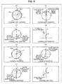
- the complex plane H1 of FIG. 5 shows reception points on the complex plane upon receiving a known sequence inserted in the input signal with the channels of the input signal not inverted. If it is assumed that a symbol in the beginning of the known sequence is a symbol A1, the second symbol is a symbol B1, the third symbol is a symbol C1, and the fourth symbol is a symbol D1, the reception points on the complex plane in the received sequences corresponding to the symbols A1, B1, C1 and D1 are: point A ⁇ 1 ⁇ N cos ⁇ / 4 + ⁇ , jsin ⁇ ⁇ / 4 + ⁇ , point B ⁇ 1 ⁇ N - sin ⁇ / 4 + 2 ⁇ ⁇ , jcos ⁇ ⁇ / 4 + 2 ⁇ ⁇ , point C ⁇ 1 ⁇ N - cos ⁇ / 4 + 3 ⁇ ⁇ , - jsin ⁇ ⁇ / 4 + 3 ⁇ ⁇ point D ⁇ 1 ⁇ N sin ⁇ / 4 +
- the known delay detection value and the received delay detection value corresponding to the known sequence come closer to the same phase as the value of ⁇ decreases, as shown in the complex planes H2 and H3 in FIG 5 , and positive correlation becomes higher.
- the correlation value at peak timing is Ke j( ⁇ /2+ ⁇ ) (where K is a value obtained by subtracting one from the number of symbols in the known sequence, the same as that in the expression (1)), and may be expressed, as shown in the complex plane of H4 in FIG. 5 , at an angle of + ⁇ relative to the positive direction of the Q axis.
- reception points on the complex plane are: point A ⁇ 1 ⁇ R cos ⁇ / 4 - ⁇ , jsin ⁇ ⁇ / 4 - ⁇ , point B ⁇ 1 ⁇ R sin ⁇ / 4 - 2 ⁇ ⁇ , - jcos ⁇ ⁇ / 4 - 2 ⁇ ⁇ , point C ⁇ 1 ⁇ N - cos ⁇ / 4 - 3 ⁇ , - jsin ⁇ ⁇ / 4 - 3 ⁇ ⁇ point D ⁇ 1 ⁇ R - sin ⁇ / 4 - 4 ⁇ ⁇ ⁇
- the phase is rotated by ⁇ - ⁇ relative to the known delay detection value of the known sequence.
- the correlation value at peak timing is given as Ke j(- ⁇ /2- ⁇ ) , and can be expressed at an angle of - ⁇ relative to the negative direction of the Q axis, as shown in the complex plane H8 in FIG 5 .
- the frame synchronization determination unit 53 detects a peak of the correlation value. Specifically, the frame synchronization determination unit 53 detects the peak value of the correlation value appealing at intervals of the frame period and the peak timing.
- step S24 the frame synchronization determination unit 53 performs frame synchronization determination. For example, if there has continued, in a predetermined time period, the state in which the peak value of the correlation value equal to or greater than a predetermined threshold appears at a predetermined frame period, the frame synchronization determination unit 53 determines that the frame synchronization has been established. The frame synchronization determination unit 53 then supplies the phase synchronization unit 38 and the channel inversion detection unit 51 with a signal indicating the status of frame synchronization, i.e., indicating the presence or absence of the establishment of frame synchronization.
- the frame synchronization determination unit 53 supplies the phase synchronization unit 38 with a signal indicating, for example, the top position of each frame in the input signal. Furthermore, the frame synchronization determination unit 53 supplies the channel inversion detection unit 51 with a signal indicating the peak timing of the correlation value.
- step S12 the phase synchronization unit 38 corrects, in step S13, the phase error of each symbol of the input signal, and supplies the error correction unit 39 with the corrected signal.
- step S14 the error correction unit 39 performs, to the input signal, LDPC and BCH decoding, or an error correction process (FEC (Forward Error Correction)), etc. such as Viterbi decoding, Reed-Solomon decoding etc., and outputs the resulting TS (transport stream) packets to a downstream device.
- FEC Forward Error Correction
- the error correction unit 39 supplies the channel inversion detection unit 51 of the frame synchronization unit 37 with a signal indicating the decoding synchronization status resulting from the error correction and decoding process.
- step S15 the tuner 12 determines whether or not the next signal is received via the antenna 11, and if it is determined that the next signal exists, the process returns to step S1, and the subsequent processes are repeated. If it is determined that there is no next signal in step S15, the process is terminated.
- the channel inversion control unit 35 is provided at the downstream configuration for establishing synchronization of a frequency and a clock signal, i.e., at the downstream of the frequency synchronization unit 32 and the clock synchronization unit 33. Therefore, even if the switching of the I channel signal and the Q channel signal is instructed, the channel inversion control unit 35 can maintain the state of the established synchronization of the frequency and the clock signal when switching the channels. As a result, in the demodulation process, even if the I channel signal and the Q channel signal are inverted, since it is not necessary to establish the synchronization of the frequency and the clock along with the switching of the I channel signal and the Q channel signal, the delay is not caused by the time required for the establishment of the synchronization. Therefore, it becomes possible to realize the demodulation process in the process time substantially equivalent to that in a case where the inversion of the Q channel signal and the I channel signal does not occur.
- step S61 the channel inversion detection unit 51 determines whether or not the power of the correlation value is equal to or larger than a predetermined threshold.
- the power of the correlation value becomes larger as the absolute value of the correlation value increases, and ideally the correlation value at peak timing is K 2 .
- the larger the power of the correlation value is the larger the absolute value of the correlation value becomes. That is, there can be observed strong correlation between the known delay detection sequence and the received delay detection sequence, indicating high reliability of the correlation value. If it is determined that the power of the correlation value is equal to or greater than a predetermined threshold, the channel inversion detection unit 51 assumes that the reliability of the correlation value is high, and the process proceeds to step S62.
- step S62 the channel inversion detection unit 51 determines whether or not the I channel signal and the Q channel of the input signal are inverted. In particular, by determining whether or not the value of the imaginary part of the correlation value is equal to or greater than zero, the channel inversion detection unit 51 determines whether or not the I channel signal and the Q channel of the input signal are inverted.
- the correlation value at peak timing is given as Ke j( ⁇ /2+ ⁇ ) .
- the correlation value at peak timing is given as Ke j(- ⁇ /2- ⁇ ) .
- the channels of the input signal are not inverted and if ⁇ falls within the range of ⁇ /2, the value of the imaginary part of the correlation value at peak timing is positive, and the correlation between the known delay detection sequence and the received delay detection sequence corresponding to the known sequence becomes a positive correlation, as shown in the shaded area in the left-hand view of FIG. 7 .
- the values of the imaginary part of the correlation value at peak timing are negative, and the correlation between the known delay detection sequence and the received delay detection sequence corresponding to the known sequence is a negative correlation, as shown in the shaded area in the right-hand view of FIG. 7 .
- the channel inversion detection unit 51 determines that the channels of the input signal have been inverted, if the value of the imaginary part of the correlation value at peak timing is less than zero under the condition that ⁇ falls within the range of ⁇ /2, and then the process proceeds to step S63.
- step S63 the channel inversion detection unit 51 generates a channel inversion detection signal indicating occurrence of the inversion of the channels, and supplies the generated channel inversion detection signal to the channel inversion control unit 35.
- the channel inversion control unit 35 assumes that the switching of the I channel signal and the Q channel signal has been instructed with regard to the input signal successively supplied thereto, in a step S7 as described above.
- step S64 the frame synchronization determination unit 53 determines whether or not it is the timing for the top position of the frame, and repeats the same process until the timing for the top position of the frame is reached.
- the process proceeds to step S65.
- step S65 the frame synchronization determination unit 53 generates a frame start signal at the timing for the top position of the frame and supplies the channel inversion control unit 35 therewith.
- the channel inversion control unit 35 switches the I channel signal and the Q channel signal as to the input signals successively supplied thereto, at the timing when the frame start signal is supplied, as described with reference to steps S8 and S9 described above.
- the I channel signal and the Q channel signal are switched at the timing when the frame start signal is supplied thereto, for example, as shown at time T1 in the upper part of FIG. 8 , the I channel signal and the Q channel signal are to be switched in the middle of reading of a header portion, resulting in the reading of the header portion susceptible to errors.
- the I channel signal and the Q channel signal are to be switched at the timing when the frame start signal is supplied thereto, so that the switching can be performed at the timing when the demodulation of the top position of the header portion is started, and therefore, it is possible to suppress the occurrence of errors. It should be noted that FIG.
- FIG 8 shows the read timing of the sequence of the header portion and the data portion frame-by-frame, in which the shaded area shows the range of demodulation after the switching of the I channel signal and the Q channel signal. Further, the state of reading the header portion at the timing different from the frame start is shown in the upper part of FIG 8 , and in the middle part thereof, the state of reading the header portion at the timing of the frame start is shown. Further, in the lower part of FIG 8 , frame start timing is indicated by arrows.
- step S62 the channel inversion detection unit 51 determines that channels of the input signal have not been inverted if the value of the imaginary part of the correlation value at peak timing is equal to or greater than zero, under the condition that ⁇ falls within the range of ⁇ /2. As a result, the processes of steps S63 through S65 are skipped. That is, the channel inversion detection unit 51 does not output a channel inversion detection result indicating that the channels of the input signal are inverted, to the channel inversion control unit 35. Alternatively, the channel inversion detection unit 51 outputs a channel inversion detection result indicating that the channels of the input signal are not inverted, to the channel inversion control unit 35.
- the frame synchronization determination unit 53 does not output a frame start signal to the channel inversion control unit 35, either.
- the channel signals are not switched and the subsequent demodulation process is continued, as described in step S10 in FIG 3 .
- step S61 if the power of the correlation value is determined to be less than a predetermined threshold, the channel inversion detection unit 51 assumes that the reliability of the correlation value is low, and the process proceeds to step S66.
- step S66 based on the signal from the error correction unit 39 and the frame synchronization determination unit 53, the channel inversion detection unit 51 determines whether or not frame synchronization and decoding synchronization are both established. In step S66, if it is determined that either the frame synchronization or the decoding synchronization is not established, the process proceeds to step S67.
- step S67 the channel inversion detection unit 51 determines whether or not a predetermined time period has elapsed. If it is determined that the predetermined time period has not elapsed, that is, if the predetermined time period has not elapsed under a state where neither the decoding synchronization nor the frame synchronization is established, the process returns to step S66. Then, the processes of steps S66 and S67 are repeatedly executed until it is determined both frame synchronization and decoding synchronization have been established in step S66, or until it is determined that a predetermined time period has elapsed in step S67.
- step S67 if it is determined, in step S67, that a predetermined time period has elapsed, i.e., that a predetermined time period has elapsed under the state in which neither the decoding synchronization nor the frame synchronization is established, the process proceeds to step S68.
- step S68 the channel inversion detection unit 51 generates a channel inversion detection signal indicating that the inversion of the channels occurs, and supplies the channel inversion detection signal to the channel inversion control unit 35.
- step S69 the frame synchronization determination unit 53 determines whether or not the timing of the top position of the frame arrives, and repeats the same process until the arrival of the timing of the top position of the frame.
- step S69 that it is proper timing of the top position of the frame, the process proceeds to step S70.
- step S70 the frame synchronization determination unit 53 generates a frame start signal at the timing of the top position of the frame, and supplies the frame start signal to the channel inversion control unit 35, and the process returns to step S66. That is, as described with reference to the above steps S8 and S9, by this process, the channel inversion control unit 35 switches the I channel signal and the Q channel signal at the timing when the frame start signal is supplied, with regard to the input signal sequentially supplied thereto.
- step S66 the processes in steps S66 through S70 are repeatedly executed until it is determined that both the decoding synchronization and the frame synchronization are established.
- the channels of the input signal are switched at predetermined time intervals until the decoding synchronization and the frame synchronization are established.
- step S66 if it is determined that both of the decoding synchronization and the frame synchronization are established, the channel control process is terminated.
- steps S66 through S70 there has been described an example for determining whether or not to synchronize both of the decoding synchronization and the frame synchronization, however, switching of the channels of the input signal may be controlled based on the state of only one of them.
- the reliability of the correlation value may be determined based on the magnitude of the direct correlation value instead of the power of the correlation value.
- the reliability of the correlation value may be determined based on whether or not the argument of the correlation value is within a predetermined range, instead of the power of the correlation value. That is, in step S61, the channel inversion detection unit 51 may determine whether the argument of the correlation value is within a predetermined range, and then, determine the reliability of the correlation value on the basis of the determination result.
- the channel inversion detection unit 51 determines that the argument of the correlation value is within the predetermined range, and accordingly, the reliability of the correlation value is regarded as sufficiently high, and the process may proceed to step S62, and the process S62 and following processes may be executed.
- the reliability of the correlation value is determined to be high, and switching of the channels of the input signal is controlled based on the value of the imaginary part of the correlation value.
- step S61 if the argument of the correlation value does not satisfy the condition of the expression (4), i.e., the argument of the correlation value is outside the range indicated by hatched lines in FIG 9 , the channel inversion detection unit 51 determines the argument of the correlation value is outside the predetermined range, so that the reliability of the correlation value is considered to be low. Then the process proceeds to step S66, and also the processes of steps S66 onward are executed.
- the reliability of the correlation value is determined to be low, and switching of the channels of the input signal is controlled not using the correlation value but based on the results of frame synchronization and decoding synchronization in the subsequent stage.
- the determination process can be realized with a simple circuit configuration, and a smaller circuit can be achieved.
- the time required for establishing the frequency and clock synchronization is generally only necessary until the first synchronization is established, and is substantially zero once the synchronization is established while the state is maintained. Therefore, as in the demodulation device 14 of FIG 1 , the channel inversion control unit 35 for switching the I channel signal and the Q channel signal is provided at the downstream configuration for establishing the synchronization of the frequency and the clock, so that even if the channels of the input signal are inverted, it is possible to switch the channels, while maintaining the state in which the frequency and clock synchronization is established. Thus, it becomes possible to prevent the delay of demodulation according to the establishment of the synchronization of the frequency and the clock.
- the delay to be considered is only the time from the timing at which the inversion of the channels is detected, to the timing at which the frame start signal is transmitted. Consequently, even if inversion of the I channel signal and the Q channel signal has occurred, the time required for the demodulation process can be substantially equal to the time when the inversion of the I channel signal and the Q channel has not occurred.
- channel inversion control unit 35 is arranged between the reception filter 34 and the equalizer 36; however, it is also possible to obtain the similar effect as described in the above with the arrangement in another location, if it is within a range within the downstream of the frequency synchronization unit 32 and the clock synchronization unit 33 and the upstream of the error correction unit 39. That is, arrangement in any location will do if it is in the downstream of the configuration for establishing the synchronization of the frequency and the clock and the upstream of the error correction unit 39 that confirms the decoding synchronization state of the TS, which is the final data.
- the method of calculating the correlation value is not limited to the above-described method, and there can be employed other methods capable of calculating the correlation value showing the direction and magnitude of the correlation of the known delay detection sequence and the received delay detection sequence.
- the correlation value between the known delay detection sequence and the received delay detection sequence corresponding to the known sequence is not necessarily the peak value due to the impact of the noise and frequency error, it can be determined whether or not the channels of the input signal is inverted, based on the value of the imaginary part of the correlation value between the known delay detection sequence and the received delay detection sequence corresponding to the known sequence.
- the present technique can be applied, for example, to a demodulation device for demodulating a signal modulated by the DVB-S.2 standard, and also to a device including the demodulation device (e.g., satellite broadcast receiving device).
- a demodulation device for demodulating a signal modulated by the DVB-S.2 standard
- a device including the demodulation device e.g., satellite broadcast receiving device
- the present technique can be applied to a demodulation device for demodulating an input signal modulated by the standard in which the difference of the correlation between the received sequence and the known sequence appears clearly in the cases where the channels of the input signal are inverted and not inverted, in addition to of the DVB-S.2 standard, and a device including the demodulation device.
- the series of processes described above can be executed by hardware but can also be executed by software.
- a program that constructs such software is installed into a computer.
- the expression "computer” includes a computer in which dedicated hardware is incorporated and a general-purpose personal computer or the like that is capable of executing various functions when various programs are installed.
- FIG. 10 is a block diagram showing a hardware configuration example of a computer that performs the above-described series of processes using a program.
- a central processing unit (CPU) 1001, read only memory (ROM) 1002 and random access memory (RAM) 1003 are mutually connected by a bus 1004.
- An input/output interface 1005 is also connected to the bus 1004.
- An input unit 1006, an output unit 1007, a storage unit 1008, a communication unit 1009, and a drive 1010 are connected to the input/output interface 1005.
- the input unit 1006 is configured from a keyboard, a mouse, a microphone or the like.
- the output unit 1007 is configured from a display, a speaker or the like.
- the storage unit 1008 is configured from a hard disk, a non-volatile memory or the like.
- the communication unit 1009 is configured from a network interface or the like.
- the drive 1010 drives a removable medium 1011 such as a magnetic disk, an optical disk, a magneto-optical disk, semiconductor memory or the like.
- the CPU 1001 loads a program that is stored, for example, in the storage unit 1008 onto the RAM 1003 via the input/output interface 1005 and the bus 1004, and executes the program.
- a program that is stored, for example, in the storage unit 1008 onto the RAM 1003 via the input/output interface 1005 and the bus 1004, and executes the program.
- Programs to be executed by the computer are provided being recorded in the removable medium 1011 which is a packaged medium or the like. Also, programs may be provided via a wired or wireless transmission medium, such as a local area network, the Internet or digital satellite broadcasting.
- the program can be installed in the storage unit 1008 via the input/output interface 1005. Further, the program can be received by the communication unit 1009 via a wired or wireless transmission medium and installed in the storage unit 1008. Moreover, the program can be installed in advance in the ROM 1002 or the storage unit 1008.
- program executed by a computer may be a program that is processed in time series according to the sequence described in this specification or a program that is processed in parallel or at necessary timing such as upon calling.
- a system has the meaning of a set of a plurality of configured elements (such as an apparatus or a module (part)), and does not take into account whether or not all the configured elements are in the same casing. Therefore, the system may be either a plurality of apparatuses, stored in separate casings and connected through a network, or a plurality of modules within a single casing.
- the present technique can adopt a configuration of cloud computing which processes by allocating and connecting one function by a plurality of apparatuses through a network.
- each step described by the above mentioned flow charts can be executed by one apparatus or by allocating a plurality of apparatuses.
- the plurality of processes included in this one step can be executed by one apparatus or by allocating a plurality of apparatuses.
- present technology may also be configured as below.
Abstract
Description
- The present technique relates to a demodulation device, a demodulation method and a program, and in particular, relates to a demodulation device, a demodulation method and a program capable of realizing a demodulation process at a rate equivalent to a case where an I channel and a Q channel are not inverted, even when the I channel and the Q channel are inverted.
- A tuner that receives a digitally modulated signal inputs a signal to a demodulation device that demodulates a digitally modulated signal, and an I channel (in-phase component) and a Q channel (quadrature component) of the input signal may be inverted, preventing normal demodulation of the input signal as it is.
- Therefore, techniques have been proposed for fixing the inversion within the demodulation device when the channels of the input signal are inverted (for instance, see
Patent Literature 1 and Patent Literature 2). In particular, a technique to quickly detect channel inversion has been proposed inPatent Literature 2. -
- Patent Literature 1:
JP H5-160863A - Patent Literature 2:
JP 2008-278173 A - However, the technique of
Patent Literature 2 switches the channels (also referred to as inversion control) and reprocesses all from the beginning after detecting the channel inversion, in order to perform demodulation process. Therefore, due to the need to reestablish the synchronization of the frequency and clock each time the channels are switched, demodulation process time sometimes becomes longer when the inversion of the channels has occurred than when there is no inversion of the channels. - The present technique has been devised in view of the above circumstances, and is intended, in particular when channels are inverted, to realize a demodulation process at a rate equivalent to a case where channels are not inverted, even when channels are inverted, through performing the inversion control to the downstream process which is the clock synchronization or the frequency synchronization.
- According to an aspect of the present disclosure, there is provided a demodulation device that demodulates an input signal split into two signals of an I channel and a Q channel, the demodulation device including a frequency correction unit that corrects a frequency of the input signal and synchronizes the frequency, an inversion detection unit that detects the I channel and the Q channel of the input signal are inverted, and a channel control unit that switches, if it is detected that the I channel and the Q channel are inverted by the inversion detection unit, the I channel and the Q channel at a downstream of the frequency correction unit.
- The channel control unit may switch channels of the input signal at timing from which a frame of the input signal changes.
- The channel control unit may again switch channels of the input signal, if frame synchronization to the input signal is not established within a predetermined time period after switching channels of the input signal.
- According to an aspect of the present disclosure, there is provided a demodulation method of a demodulation device that demodulates an input signal split into two signals of an I channel and a Q channel, the demodulation method including the steps of executing a frequency correction process that corrects frequency of the input signal and synchronizes the frequency, executing an inversion detection process that detects the I channel and the Q channel of the input signal are inverted, and executing a channel control process that switches, if it is detected that the I channel and the Q channel are inverted in the inversion detection process, the I channel and the Q channel in a downstream process of the frequency correction process.
- According to an aspect of the present disclosure, there is provided a program for causing a computer controlling a demodulation device that demodulates an input signal split into two signals of an I channel and a Q channel, to function as a frequency correction unit that corrects a frequency of the input signal and synchronizes the frequency, an inversion detection unit that detects the I channel and the Q channel of the input signal are inverted, and a channel control unit that switches, if it is detected that the I channel and the Q channel are inverted by the inversion detection unit, the I channel and the Q channel at a downstream of the frequency correction unit.
- According to one aspect of the present technique, there is provided a frequency correction unit that corrects the frequency of an input signal and synchronizes the frequency, and inversion of the I channel and the Q channel being the input signal is detected. When the inversion of the I channel and the Q channel is detected, in a process subsequent to a configuration for establishing synchronization by frequency correction, the I channel and the Q channel are switched.
- A demodulation device of the present technique may be an independent device, or may be a block that performs a demodulation process.
- According to one aspect of the present technique, even if the I channel signal and the Q channel signal are input under an inverted state, it is possible to realize a demodulation process at a rate equivalent to that in a non-inverted state.
-
- [
FIG. 1] FIG. 1 is a block diagram showing a configuration example of an embodiment of a demodulation device according to the present technique. - [
FIG. 2] FIG. 2 is a diagram showing a mapping pattern in a complex plane for each symbol in π/2 shift BPSK. - [
FIG. 3] FIG. 3 is a flowchart for explaining a demodulation process performed by the demodulation device ofFIG. 1 . - [
FIG. 4] FIG. 4 is a flowchart for explaining a frame synchronization process performed by the demodulation device ofFIG. 1 . - [
FIG. 5] FIG. 5 is a diagram showing a relation of presence or absence of inversion in the channels of the input signal, reception points on the complex plane when a known sequence inserted into the input signal is received, a known delay detection value and a received delay detection value of a received sequence corresponding to the known sequence. - [
FIG. 6] FIG. 6 is a flow chart for explaining a channel control process executed by the demodulation device ofFIG. 1 . - [
FIG. 7] FIG. 7 is a diagram for explaining a determination process in step S62 in the flowchart ofFIG. 6 . - [
FIG. 8] FIG. 8 is a diagram explaining a reason for switching channels at timing when a frame start signal is supplied. - [
FIG. 9] FIG. 9 is a diagram for explaining a determination process of step S61 inFIG 6 . - [
FIG. 10] FIG. 10 is a diagram for explaining a configuration example of a general-purpose personal computer. -
FIG. 1 is a block diagram illustrating an embodiment of a receiving system including a demodulation device according to the present technique. The reception system ofFIG 1 is a system for receiving and demodulating a broadcast signal that are in conformity with DVB-S.2 standard (hereinafter also referred to as input signal). - The DVB-S.2 standard is a standard above DVB-S standard standardized by ETSI (European Telecommunications Standards Institute) for general use. The DVB-S.2 standard, as compared with the DVB-S standard, seeks to improve efficiency of frequency utilization and to improve C/N ratio (Carrier to Noise ratio) per frequency unit, through introducing multiple phase shift keying or LDPC (Low Density Parity Check) code. Further, synchronization pilot signal or PL (physical layer) header for transmitting the transmission information on a physical layer has been introduced as a standard, in order to ensure synchronization performance at low C/N ratio.
- In the DVB-S.2 standard, the PL header and the synchronization pilot signal are modulated by π/2 shift BPSK (Binary Phase Shift Keying) and transmitted.
FIG. 2 is a view showing a mapping pattern for each symbol in the π/2 shift BPSK on a complex plane. A mapping pattern of odd numbered symbols is shown on the left side ofFIG. 2 , and a mapping pattern of even numbered symbols is shown on the right side thereof. That is, on the complex plane, the odd numbered symbols are mapped in such a manner that the argument is π/4 when the value is zero, and the argument is 5π/4 when the value is one, and the even numbered symbols are mapped in such a manner that, the argument is 3π/4 when the value is zero, and the argument is 7π/4 when the value is one. Therefore, the phase difference between the adjacent symbols is limited to ±π/2. - Referring back to
FIG. 1 , the receiving system is configured to include anantenna 11, atuner 12, A/D converters 13-1, 13-2, and ademodulation device 14. - The
tuner 12 receives an input signal conforming to the DVB-S.2 standard via theantenna 11, separates the received input signal into two signals of I channel and Q channel, and supplies the separated signals to the A/D converters 13-1, 13-2, respectively. Hereinafter, a signal of the I channel is also referred to as an I channel signal, and a signal of the Q channel is also referred to as a Q channel signal. - The A/D converters 13-1 and 13-2 convert the I channel signal or the Q channel signal being an input signal from an analog signal into a digital signal, and supplies the converted signal to a
frequency correction unit 31 of thedemodulation device 14. - The
demodulation device 14 is structured to include afrequency correction unit 31, afrequency synchronization unit 32, aclock synchronization unit 33, areception filter 34, a channelinversion control unit 35, anequalizer 36, aframe synchronization unit 37, aphase synchronization unit 38, and anerror correction unit 39. - According to the correction signal supplied from the
frequency synchronization unit 32, thefrequency correction unit 31 corrects the frequency of the input signal, and supplies the corrected input signal to theclock synchronization unit 33. Theclock synchronization unit 33 synchronizes, with the clock signal, the input signal whose frequency is corrected by thefrequency correction unit 31, supplies the synchronized input signal to thefrequency synchronization unit 32 and thereception filter 34. Thefrequency synchronization unit 32 obtains a correction amount that is required to synchronize the frequency of the input signal with a predetermined frequency, and supplies thefrequency correction unit 31 with the obtained correction amount as a correction signal. In other words, synchronization of the clock and the frequency of the input signal is established by a loop of thefrequency correction unit 31, thefrequency synchronization unit 32 and theclock synchronization unit 33. - The
reception filter 34 is, for example, a roll-off filter, and provides the channelinversion control unit 35 with the result of the filtering. - According to the channel inversion detection result supplied from a channel
inversion detection unit 51 of theframe synchronization unit 37, the channelinversion control unit 35 switches and outputs the I channel signal and the Q channel signal being the input signal supplied from thereception filter 34. Further, if it is necessary to switch the I channel signal and the Q channel signal according to the channel inversion detection result, the channelinversion control unit 35 switches the I channel signal and the Q channel signal, at the timing of obtaining a frame start signal supplied from a frame synchronization determination unit 53 of theframe synchronization unit 37, and supplies the switched I channel signal and the Q channel signal to theequalizer 36. - The
equalizer 36 restores each component degraded on the transmission path associated with the transmission with regard to the I channel signal and the Q channel signal supplied from the channelinversion control unit 35, and supplies the restored I channel signal and Q channel signal to theframe synchronization unit 37. - The
frame synchronization unit 37 performs synchronization control to the input signal per frame unit. Theframe synchronization unit 37 supplies thephase synchronization unit 38 with the input signal supplied from theequalizer 36 as it is. Further, theframe synchronization unit 37 includes the channelinversion detection unit 51, acorrelation detection unit 52, and the frame synchronization determination unit 53, and performs channel control along with the synchronization control. - The channel
inversion detection unit 51 detects whether or not the phases of I channel and Q channel of the signal to be output to thephase synchronization unit 38 are in a right relation, i.e., the phase of Q channel is delayed by π/2 with respect to the phase of I channel. More specifically, the channelinversion detection unit 51 detects whether or not the relation of the phases of the I and Q channels are correct according to the correlation value from thecorrelation detection unit 52, the determination result of the reliability of the correlation value, a synchronization state of the frame notified from the frame synchronization determination unit 53, or the state of the decoding synchronization by the error correction process which is notified from theerror correction unit 39. Then, the channelinversion detection unit 51 supplies the channelinversion control unit 35 with the detection result as the channel inversion detection result. Based on the channel inversion detection result, when the phase relation is not correct and needs switching, the channelinversion control unit 35 switches the channels of the input signal. - As used herein, the term switching the channels of the input signal means that reversing the phase relation of the I channel signal and the Q channel signal input to the channel
inversion control unit 35 from thereception filter 34. For example, methods of switching the channels of the input signal includes a method such as switching, by a selector, the signal output from each output terminal, and a method of reversing, by an inverter, the phases by inverting the polarity of one of the signals output from each output terminal. - The
correlation detection unit 52 performs delay detection to the complex symbol sequence of the input signal (hereinafter, also referred to as a received sequence), through performing complex multiplication of the complex conjugate of the symbol preceding the current symbol and the current symbol. Thecorrelation detection unit 52 correlates a symbol sequence of the received delay detection value - (hereinafter, also referred to as a received delay detection sequence), and a symbol sequence (hereinafter, also referred to as a known delay detection sequence) of a correct delay detection value (hereinafter, also referred to as a known delay detection value) of a symbol sequence of a known value (hereinafter, also referred to as a known sequence) that is periodically inserted in the input signal, such as a portion of the PL header or a synchronization pilot signal, and supplies the resulting correlation value to the channel
inversion detection unit 51 and the frame synchronization determination unit 53. Thecorrelation detection unit 52 determines the reliability of the correlation value, and notifies the channelinversion detection unit 51 of the determination result. - In the following, an explanation is given assuming that the
correlation detection unit 52 calculates, regarding a sequence SOF (Start Of Frame) in PL header inserted at the beginning of each header in the input signal as a known sequence, the correlation value between the known delay detection sequence corresponding to the known sequence and the received delay detection sequence. - The frame synchronization determination unit 53 detects a peak value of the correlation value appearing in a frame period and the timing thereof (hereinafter, also referred to as peak timing).
- The frame synchronization determination unit 53 synchronizes the input signal for a frame unit according to a peak value and peak timing of the detected correlation value. The frame synchronization determination unit 53 supplies a frame synchronization status, and a signal indicating the peak timing of the correlation value to the channel
inversion detection unit 51. Further, the frame synchronization determination unit 53 supplies thephase synchronization unit 38 with a frame synchronization status and a signal indicating, for example, the top position of each frame of the input signal. Furthermore, the frame synchronization determination unit 53 supplies the channelinversion control unit 35, as a frame start signal, information of the top position of each frame. - The
phase synchronization unit 38 corrects the phase error of each symbol of the input signal, and supplies the corrected signal to theerror correction unit 39. - The
error correction unit 39 applies, to the input signal, LDPC or BCH decoding, or error correction (FEC (Forward Error Correction)), etc. such as Viterbi decoding, Reed-Solomon decoding, etc., and TS (Transport stream) packets obtained as a result is output to a downstream device. Further, theerror correction unit 39 supplies the channelinversion detection unit 51 of theframe synchronization unit 37 with a signal indicating the decoding synchronization status resulting from an error correction and decoding process. - Next will be described a demodulation process by the receiving system of
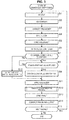
FIG. 1 with reference to the flowchart ofFIG 3 . - In step S1, the
tuner 12 receives an input signal in conformity with the DVB-S.2 standard via theantenna 11, splits the received input signal into two signals of I and Q channels, and supplies the A/D converters 13-1 and 13-2 therewith. - In step S2, the A/D converters 13-1 and 13-2 convert the input I channel signal or Q channel signal from an analog signal into a digital signal, and supply the converted signals to the
frequency correction unit 31 of thedemodulation device 14. - In step S3, the
frequency correction unit 31 corrects the frequency of the input I channel and Q channel signal converted into a digital signal, according to the correction signal indicating the correction amount supplied from thefrequency synchronization unit 32, and supplies the I channel signal and the Q channel signal to theclock synchronization unit 33. - In step S4, the
clock synchronization unit 33 synchronizes, with a predetermined clock signal, the I channel signal and the Q channel signal converted into a digital signal, corrected with regards to the frequency thereof, and supplied from thefrequency correction unit 31, and supplies the I channel signal and the Q channel signal to thefrequency synchronization unit 32 and thereception filter 34. - In step S5, the
frequency synchronization unit 32 generates a signal indicating a correction amount of the frequency of the I channel signal and the Q channel signal synchronized to the clock, and supplies the signal to thefrequency correction unit 31. - That is, the same process is repeated by a loop constituted by the
frequency correction unit 31, thefrequency synchronization unit 32 and theclock synchronization unit 33, so that the frequency and clock synchronization is established. However, generally, with regard to the frequency and clock synchronization, once a condition is established, the established condition is continued. - In step S6, the
reception filter 34 applies, for example, a roll-off filter to the I channel signal and the Q channel signal with synchronized frequency and clock, which are supplied from theclock synchronization unit 33, and supplies the I channel signal and the Q channel signal to the channelinversion control unit 35. - In step S7, the channel
inversion control unit 35 determines whether or not there has been supplied a channel inversion detection result indicating that the I channel signal and the Q channel signal are inverted by the channelinversion detection unit 51 of theframe synchronization unit 37. In step S8, for example, if the process of steps S63 and S68 inFIG 6 described below has supplied, from the channelinversion detection unit 51, the channel inversion detection result indicating that the I channel signal and the Q channel signal are inverted, the process proceeds to step S8. - In step S8, the channel
inversion control unit 35 determines whether or not a frame start signal has been supplied from the frame synchronization determination unit 53, and repeats the same process until the frame start signal is transmitted. Then, in step S8, when a frame start signal is supplied thereto by the processes of, for example, steps S65, S70 ofFIG 6 described below, the process proceeds to step S9. - In step S9, the channel
inversion control unit 35 inverts the I channel signal and the Q channel signal supplied from thereception filter 34 and supplies the inverted I channel signal and Q channel signal to theequalizer 36. - Meanwhile, in step S7, if there has not been supplied a channel inversion detection result indicating that the I channel signal and the Q channel signal are inverted, from the channel
inversion detection unit 51 of theframe synchronization unit 37, the process proceeds to step S10. - In step S10, the channel
inversion control unit 35 supplies, to theequalizer 36, the I channel signal and the Q channel signal supplied from thereception filter 34 as they are without inverting. - In step S11, the
equalizer 36 restores components degraded on the transmission path associated with the transmission, respectively, of the I channel signal and the Q channel signal supplied from the channelinversion control unit 35, and supplies the restored I channel signal and Q channel signal to theframe synchronization unit 37. - In step S12, the
frame synchronization unit 37 executes the frame synchronization process, synchronizes the input signal frame by frame, and supplies, to thephase synchronization unit 38, the input signal supplied from theequalizer 36 as it is. - Referring now to the flowchart of
FIG 4 , there will be described frame synchronization process by theframe synchronization unit 37. - In step S21, the
correlation detection unit 52 performs delay detection. In particular, thecorrelation detection unit 52 performs delay detection by performing a complex multiplication of the complex conjugate of the current symbol and the delayed symbol which is one symbol before the current symbol to the input signal, and determines the received delay detection value. - In step S22, the
correlation detection unit 52 calculates a correlation value. Specifically, thecorrelation detection unit 52 calculates a correlation value representing the correlation between a received delay detection sequence and a known delay detection sequence using the following mathematical expression (1): - [Math. 1]

- Here, K is a value obtained by subtracting one from the number of symbols of the known sequence inserted in the beginning of each frame of the input signal. Further, di denotes the i-th value in the received delay detection sequence.
- The
correlation detection unit 52 supplies the calculated correlation value to the frame synchronization determination unit 53 and the channelinversion detection unit 51. - Meanwhile, the difference between the correlation value when the channels of the input signal are not inverted and the correlation value when inverted is discussed.
- First, the case where the channels of the input signal are not inverted is considered. In order to simplify the explanation, the value of the known sequence inserted in the input signal is regarded as 0011, and then the value of the known delay detection sequence corresponding to the known sequence is regarded as j, j, j.
- The complex plane H1 of
FIG. 5 shows reception points on the complex plane upon receiving a known sequence inserted in the input signal with the channels of the input signal not inverted. If it is assumed that a symbol in the beginning of the known sequence is a symbol A1, the second symbol is a symbol B1, the third symbol is a symbol C1, and the fourth symbol is a symbol D1, the reception points on the complex plane in the received sequences corresponding to the symbols A1, B1, C1 and D1 are:


Here, Δθ denotes the phase rotational angle per symbol caused by frequency error. - In the above case, the delay detection value between adjacent symbols in the received sequence corresponding to the known sequence (i.e., received delay detection value) is given as B1N.A1N*=C1N.B1N*=D1N.C1N*=ej(π/2+Δθ), and as shown in the complex plane H2 in
FIG. 5 , the phase is rotated by +Δθ relative to the delay detection value of the known sequence (i.e., known delay detection value). Then, based on the expression (1) above, the correlation value between the known delay detection sequence and the received delay detection sequence corresponding to the known sequence, i.e., correlation value at peak timing, is defined by the following expression (2):
- Thus, if the channels of the input signal are not inverted, the known delay detection value and the received delay detection value corresponding to the known sequence come closer to the same phase as the value of Δθ decreases, as shown in the complex planes H2 and H3 in
FIG 5 , and positive correlation becomes higher. - Further, in an ideal reception environment, the correlation value at peak timing is Kej(π/2+Δθ) (where K is a value obtained by subtracting one from the number of symbols in the known sequence, the same as that in the expression (1)), and may be expressed, as shown in the complex plane of H4 in
FIG. 5 , at an angle of +Δθ relative to the positive direction of the Q axis. - Then, the case where the channels of the input signal are inverted is considered.
- If the channels of the input signal are inverted, the rotation direction of the phase rotation angle per symbol caused by frequency error is in the opposite direction, compared with the case where the channels of the input signal are not inverted. Thus, as shown in the complex plane H5 in
FIG. 5 , upon receiving the sequence of symbols A1, B1, C1 and D1 in the above-described known sequence whose value is 0011, reception points on the complex plane are:


- In the above case, the received delay detection value of the received sequence corresponding to the known sequence is given as B1R.A1R*=C1R.B1R*= D1R.C1R*=ej(-π/2-Δθ). As shown in the complex plane H6 in
FIG. 5 , the phase is rotated by π-Δθ relative to the known delay detection value of the known sequence. Then, based on the expression (1) above, the correlation value between the known delay detection sequence and the received delay detection sequence corresponding to the known sequence is defined by the following expression (3):
- Thus, as shown in complex planes H6 and H7 in
FIG 5 , if the channels of the input signal are inverted, the known delay detection value and the received delay detection value corresponding to the known sequence come closer to the opposite phase as the value of Δθ decreases, and negative correlation becomes higher. - Further, in an ideal reception environment, the correlation value at peak timing is given as Kej(-π/2-Δθ), and can be expressed at an angle of -Δθ relative to the negative direction of the Q axis, as shown in the complex plane H8 in
FIG 5 . - Referring back to
FIG 4 , in step S23, the frame synchronization determination unit 53 detects a peak of the correlation value. Specifically, the frame synchronization determination unit 53 detects the peak value of the correlation value appealing at intervals of the frame period and the peak timing. - In step S24, the frame synchronization determination unit 53 performs frame synchronization determination. For example, if there has continued, in a predetermined time period, the state in which the peak value of the correlation value equal to or greater than a predetermined threshold appears at a predetermined frame period, the frame synchronization determination unit 53 determines that the frame synchronization has been established. The frame synchronization determination unit 53 then supplies the
phase synchronization unit 38 and the channelinversion detection unit 51 with a signal indicating the status of frame synchronization, i.e., indicating the presence or absence of the establishment of frame synchronization. Further, if frame synchronization is found to be established, the frame synchronization determination unit 53 supplies thephase synchronization unit 38 with a signal indicating, for example, the top position of each frame in the input signal. Furthermore, the frame synchronization determination unit 53 supplies the channelinversion detection unit 51 with a signal indicating the peak timing of the correlation value. - Now, the explanation is returned to the flowchart in
FIG. 3 . - If the frame synchronization process is performed in step S12, the
phase synchronization unit 38 corrects, in step S13, the phase error of each symbol of the input signal, and supplies theerror correction unit 39 with the corrected signal. - In step S14, the
error correction unit 39 performs, to the input signal, LDPC and BCH decoding, or an error correction process (FEC (Forward Error Correction)), etc. such as Viterbi decoding, Reed-Solomon decoding etc., and outputs the resulting TS (transport stream) packets to a downstream device. At this time, theerror correction unit 39 supplies the channelinversion detection unit 51 of theframe synchronization unit 37 with a signal indicating the decoding synchronization status resulting from the error correction and decoding process. - In step S15, the
tuner 12 determines whether or not the next signal is received via theantenna 11, and if it is determined that the next signal exists, the process returns to step S1, and the subsequent processes are repeated. If it is determined that there is no next signal in step S15, the process is terminated. - That is, the channel
inversion control unit 35 is provided at the downstream configuration for establishing synchronization of a frequency and a clock signal, i.e., at the downstream of thefrequency synchronization unit 32 and theclock synchronization unit 33. Therefore, even if the switching of the I channel signal and the Q channel signal is instructed, the channelinversion control unit 35 can maintain the state of the established synchronization of the frequency and the clock signal when switching the channels. As a result, in the demodulation process, even if the I channel signal and the Q channel signal are inverted, since it is not necessary to establish the synchronization of the frequency and the clock along with the switching of the I channel signal and the Q channel signal, the delay is not caused by the time required for the establishment of the synchronization. Therefore, it becomes possible to realize the demodulation process in the process time substantially equivalent to that in a case where the inversion of the Q channel signal and the I channel signal does not occur. - Next will be described the channel control process executed in relation to the demodulation process as described above, with reference to the flowchart of
FIG. 6 . - In step S61, the channel
inversion detection unit 51 determines whether or not the power of the correlation value is equal to or larger than a predetermined threshold. The power of the correlation value becomes larger as the absolute value of the correlation value increases, and ideally the correlation value at peak timing is K2. Conversely, the larger the power of the correlation value is, the larger the absolute value of the correlation value becomes. That is, there can be observed strong correlation between the known delay detection sequence and the received delay detection sequence, indicating high reliability of the correlation value. If it is determined that the power of the correlation value is equal to or greater than a predetermined threshold, the channelinversion detection unit 51 assumes that the reliability of the correlation value is high, and the process proceeds to step S62. - In step S62, the channel
inversion detection unit 51 determines whether or not the I channel signal and the Q channel of the input signal are inverted. In particular, by determining whether or not the value of the imaginary part of the correlation value is equal to or greater than zero, the channelinversion detection unit 51 determines whether or not the I channel signal and the Q channel of the input signal are inverted. - As described above with reference to the complex plane H4 in
FIG 5 , if the channels of the input signal are not inverted, in an ideal reception environment, the correlation value at peak timing is given as Kej(π/2+Δθ). Whereas, as described above with reference to the complex plane H8 inFIG 5 , if the channels of the input signal are inverted, in an ideal reception environment, the correlation value at peak timing is given as Kej(-π/2-Δθ). Thus, if the channels of the input signal are not inverted and if Δθ falls within the range of ±π/2, the value of the imaginary part of the correlation value at peak timing is positive, and the correlation between the known delay detection sequence and the received delay detection sequence corresponding to the known sequence becomes a positive correlation, as shown in the shaded area in the left-hand view ofFIG. 7 . Whereas, if the channels of the input signal are inverted and if Δθ falls within the range of ±π/2, the value of the imaginary part of the correlation value at peak timing is negative, and the correlation between the known delay detection sequence and the received delay detection sequence corresponding to the known sequence is a negative correlation, as shown in the shaded area in the right-hand view ofFIG. 7 . - By utilizing this property, the channel
inversion detection unit 51 determines that the channels of the input signal have been inverted, if the value of the imaginary part of the correlation value at peak timing is less than zero under the condition that Δθ falls within the range of ±π/2, and then the process proceeds to step S63. - In step S63, the channel
inversion detection unit 51 generates a channel inversion detection signal indicating occurrence of the inversion of the channels, and supplies the generated channel inversion detection signal to the channelinversion control unit 35. By this process, the channelinversion control unit 35 assumes that the switching of the I channel signal and the Q channel signal has been instructed with regard to the input signal successively supplied thereto, in a step S7 as described above. - In step S64, the frame synchronization determination unit 53 determines whether or not it is the timing for the top position of the frame, and repeats the same process until the timing for the top position of the frame is reached. When it is regarded that the timing of the top position of the frame is reached in step S64, the process proceeds to step S65.
- In step S65, the frame synchronization determination unit 53 generates a frame start signal at the timing for the top position of the frame and supplies the channel
inversion control unit 35 therewith. By this process, the channelinversion control unit 35 switches the I channel signal and the Q channel signal as to the input signals successively supplied thereto, at the timing when the frame start signal is supplied, as described with reference to steps S8 and S9 described above. - That is, if the I channel signal and the Q channel signal are switched at the timing when the frame start signal is supplied thereto, for example, as shown at time T1 in the upper part of
FIG. 8 , the I channel signal and the Q channel signal are to be switched in the middle of reading of a header portion, resulting in the reading of the header portion susceptible to errors. Meanwhile, as shown at time T11 in the center part ofFIG. 8 , the I channel signal and the Q channel signal are to be switched at the timing when the frame start signal is supplied thereto, so that the switching can be performed at the timing when the demodulation of the top position of the header portion is started, and therefore, it is possible to suppress the occurrence of errors. It should be noted thatFIG. 8 shows the read timing of the sequence of the header portion and the data portion frame-by-frame, in which the shaded area shows the range of demodulation after the switching of the I channel signal and the Q channel signal. Further, the state of reading the header portion at the timing different from the frame start is shown in the upper part ofFIG 8 , and in the middle part thereof, the state of reading the header portion at the timing of the frame start is shown. Further, in the lower part ofFIG 8 , frame start timing is indicated by arrows. - Meanwhile, in step S62, the channel
inversion detection unit 51 determines that channels of the input signal have not been inverted if the value of the imaginary part of the correlation value at peak timing is equal to or greater than zero, under the condition that Δθ falls within the range of ±π/2. As a result, the processes of steps S63 through S65 are skipped. That is, the channelinversion detection unit 51 does not output a channel inversion detection result indicating that the channels of the input signal are inverted, to the channelinversion control unit 35. Alternatively, the channelinversion detection unit 51 outputs a channel inversion detection result indicating that the channels of the input signal are not inverted, to the channelinversion control unit 35. In the same way, the frame synchronization determination unit 53 does not output a frame start signal to the channelinversion control unit 35, either. As a result, the channel signals are not switched and the subsequent demodulation process is continued, as described in step S10 inFIG 3 . - On the other hand, in step S61, if the power of the correlation value is determined to be less than a predetermined threshold, the channel
inversion detection unit 51 assumes that the reliability of the correlation value is low, and the process proceeds to step S66. - In step S66, based on the signal from the
error correction unit 39 and the frame synchronization determination unit 53, the channelinversion detection unit 51 determines whether or not frame synchronization and decoding synchronization are both established. In step S66, if it is determined that either the frame synchronization or the decoding synchronization is not established, the process proceeds to step S67. - In step S67, the channel
inversion detection unit 51 determines whether or not a predetermined time period has elapsed. If it is determined that the predetermined time period has not elapsed, that is, if the predetermined time period has not elapsed under a state where neither the decoding synchronization nor the frame synchronization is established, the process returns to step S66. Then, the processes of steps S66 and S67 are repeatedly executed until it is determined both frame synchronization and decoding synchronization have been established in step S66, or until it is determined that a predetermined time period has elapsed in step S67. - On the other hand, if it is determined, in step S67, that a predetermined time period has elapsed, i.e., that a predetermined time period has elapsed under the state in which neither the decoding synchronization nor the frame synchronization is established, the process proceeds to step S68.
- In step S68, the channel
inversion detection unit 51 generates a channel inversion detection signal indicating that the inversion of the channels occurs, and supplies the channel inversion detection signal to the channelinversion control unit 35. - In step S69, the frame synchronization determination unit 53 determines whether or not the timing of the top position of the frame arrives, and repeats the same process until the arrival of the timing of the top position of the frame. When it is regarded, in step S69, that it is proper timing of the top position of the frame, the process proceeds to step S70.
- In step S70, the frame synchronization determination unit 53 generates a frame start signal at the timing of the top position of the frame, and supplies the frame start signal to the channel
inversion control unit 35, and the process returns to step S66. That is, as described with reference to the above steps S8 and S9, by this process, the channelinversion control unit 35 switches the I channel signal and the Q channel signal at the timing when the frame start signal is supplied, with regard to the input signal sequentially supplied thereto. - Then, in step S66, the processes in steps S66 through S70 are repeatedly executed until it is determined that both the decoding synchronization and the frame synchronization are established. In other words, the channels of the input signal are switched at predetermined time intervals until the decoding synchronization and the frame synchronization are established.
- On the other hand, in step S66, if it is determined that both of the decoding synchronization and the frame synchronization are established, the channel control process is terminated.
- Thus, if it is determined that the power of the correlation value is large and the reliability of the correlation value is high, switching of the channels of the input signal is controlled based on the correlation value, and if it is determined that the power of the correlation value is small, and the reliability of the correlation values is low, switching of the channels of the input signal is controlled without using the correlation value, based on the state of the subsequent frame synchronization and the decoding synchronization. Thus, it is possible to perform the switching of the channels of the input signal with higher accuracy.
- In steps S66 through S70, there has been described an example for determining whether or not to synchronize both of the decoding synchronization and the frame synchronization, however, switching of the channels of the input signal may be controlled based on the state of only one of them.
- Also, the reliability of the correlation value may be determined based on the magnitude of the direct correlation value instead of the power of the correlation value.
- Further, the reliability of the correlation value may be determined based on whether or not the argument of the correlation value is within a predetermined range, instead of the power of the correlation value. That is, in step S61, the channel
inversion detection unit 51 may determine whether the argument of the correlation value is within a predetermined range, and then, determine the reliability of the correlation value on the basis of the determination result. In particular, if the condition of the following expression (4) is met when the argument of the correlation value is expressed within a range from -π to π, i.e., if the argument of the correlation value is within a range indicated by hatched lines inFIG 9 , the channelinversion detection unit 51 determines that the argument of the correlation value is within the predetermined range, and accordingly, the reliability of the correlation value is regarded as sufficiently high, and the process may proceed to step S62, and the process S62 and following processes may be executed.
- That is, for example, if the value of Δθ is small and with a little variation, and the deflection angle of the correlation value is closer to ±π/2, the reliability of the correlation value is determined to be high, and switching of the channels of the input signal is controlled based on the value of the imaginary part of the correlation value.
- Therefore, in this case, in step S61, if the argument of the correlation value does not satisfy the condition of the expression (4), i.e., the argument of the correlation value is outside the range indicated by hatched lines in
FIG 9 , the channelinversion detection unit 51 determines the argument of the correlation value is outside the predetermined range, so that the reliability of the correlation value is considered to be low. Then the process proceeds to step S66, and also the processes of steps S66 onward are executed. - That is, for example, if the value of Δθ is large or with larger variation and the argument of the correlation value is closer to zero or π, the reliability of the correlation value is determined to be low, and switching of the channels of the input signal is controlled not using the correlation value but based on the results of frame synchronization and decoding synchronization in the subsequent stage. Thus, it becomes possible to perform the switching of the channels of the input signal with higher accuracy.
- Further, in the above discussion, an example is described in which, when the reliability of the correlation value is low, channels are switched until both the frame synchronization and the decoding synchronization are established; however, it is also possible to regard the reliability of the correlation value to be high, and to omit the processes of steps S61, and S66 through S70. Accordingly, if the channels of the input signal are inverted, the switching of channels of the input signal can be controlled based on the correlation value of the calculation results in the middle of the frame synchronization, without waiting for the result of the decoding synchronization by the
error correction unit 39 and the result of the frame synchronization in the frame synchronization determination unit 53, so that correct demodulation of the input signal can be performed more quickly. - As it is possible to determine whether or not the value of the imaginary part of the correlation value is equal to or greater than zero, for example, by the determination result of whether the uppermost bit of the correlation value is one or zero, the determination process can be realized with a simple circuit configuration, and a smaller circuit can be achieved.
- Further, the time required for establishing the frequency and clock synchronization is generally only necessary until the first synchronization is established, and is substantially zero once the synchronization is established while the state is maintained. Therefore, as in the
demodulation device 14 ofFIG 1 , the channelinversion control unit 35 for switching the I channel signal and the Q channel signal is provided at the downstream configuration for establishing the synchronization of the frequency and the clock, so that even if the channels of the input signal are inverted, it is possible to switch the channels, while maintaining the state in which the frequency and clock synchronization is established. Thus, it becomes possible to prevent the delay of demodulation according to the establishment of the synchronization of the frequency and the clock. That is, if the I channel signal and the Q channel signal have been inverted and are to be switched, the delay to be considered is only the time from the timing at which the inversion of the channels is detected, to the timing at which the frame start signal is transmitted. Consequently, even if inversion of the I channel signal and the Q channel signal has occurred, the time required for the demodulation process can be substantially equal to the time when the inversion of the I channel signal and the Q channel has not occurred. - Further, in the above discussion, an exemplary configuration is described in which the channel
inversion control unit 35 is arranged between thereception filter 34 and theequalizer 36; however, it is also possible to obtain the similar effect as described in the above with the arrangement in another location, if it is within a range within the downstream of thefrequency synchronization unit 32 and theclock synchronization unit 33 and the upstream of theerror correction unit 39. That is, arrangement in any location will do if it is in the downstream of the configuration for establishing the synchronization of the frequency and the clock and the upstream of theerror correction unit 39 that confirms the decoding synchronization state of the TS, which is the final data. - Further, the method of calculating the correlation value is not limited to the above-described method, and there can be employed other methods capable of calculating the correlation value showing the direction and magnitude of the correlation of the known delay detection sequence and the received delay detection sequence.
- In the above description, there has been described an example of using a value obtained by adding the correlation value for each delay detection value for the determination of whether or not to switch the channels of the input signal; however, for example, using the average value of the correlation values for the values of the respective delay detection is also possible.
- In addition, even if the correlation value between the known delay detection sequence and the received delay detection sequence corresponding to the known sequence is not necessarily the peak value due to the impact of the noise and frequency error, it can be determined whether or not the channels of the input signal is inverted, based on the value of the imaginary part of the correlation value between the known delay detection sequence and the received delay detection sequence corresponding to the known sequence.
- The present technique can be applied, for example, to a demodulation device for demodulating a signal modulated by the DVB-S.2 standard, and also to a device including the demodulation device (e.g., satellite broadcast receiving device).
- Further, the present technique can be applied to a demodulation device for demodulating an input signal modulated by the standard in which the difference of the correlation between the received sequence and the known sequence appears clearly in the cases where the channels of the input signal are inverted and not inverted, in addition to of the DVB-S.2 standard, and a device including the demodulation device.
- The series of processes described above can be executed by hardware but can also be executed by software. When the series of processes is executed by software, a program that constructs such software is installed into a computer. Here, the expression "computer" includes a computer in which dedicated hardware is incorporated and a general-purpose personal computer or the like that is capable of executing various functions when various programs are installed.
-
FIG. 10 is a block diagram showing a hardware configuration example of a computer that performs the above-described series of processes using a program. - In the computer, a central processing unit (CPU) 1001, read only memory (ROM) 1002 and random access memory (RAM) 1003 are mutually connected by a
bus 1004. - An input/
output interface 1005 is also connected to thebus 1004. Aninput unit 1006, anoutput unit 1007, astorage unit 1008, acommunication unit 1009, and adrive 1010 are connected to the input/output interface 1005. - The
input unit 1006 is configured from a keyboard, a mouse, a microphone or the like. Theoutput unit 1007 is configured from a display, a speaker or the like. Thestorage unit 1008 is configured from a hard disk, a non-volatile memory or the like. Thecommunication unit 1009 is configured from a network interface or the like. Thedrive 1010 drives a removable medium 1011 such as a magnetic disk, an optical disk, a magneto-optical disk, semiconductor memory or the like. - In the computer configured as described above, the
CPU 1001 loads a program that is stored, for example, in thestorage unit 1008 onto theRAM 1003 via the input/output interface 1005 and thebus 1004, and executes the program. Thus, the above-described series of processes is performed. - Programs to be executed by the computer (the CPU 1001) are provided being recorded in the removable medium 1011 which is a packaged medium or the like. Also, programs may be provided via a wired or wireless transmission medium, such as a local area network, the Internet or digital satellite broadcasting.
- Then, by inserting the removable medium 1011 into the
drive 1010, the program can be installed in thestorage unit 1008 via the input/output interface 1005. Further, the program can be received by thecommunication unit 1009 via a wired or wireless transmission medium and installed in thestorage unit 1008. Moreover, the program can be installed in advance in theROM 1002 or thestorage unit 1008. - It should be noted that the program executed by a computer may be a program that is processed in time series according to the sequence described in this specification or a program that is processed in parallel or at necessary timing such as upon calling.
- Further, in the present technique, a system has the meaning of a set of a plurality of configured elements (such as an apparatus or a module (part)), and does not take into account whether or not all the configured elements are in the same casing. Therefore, the system may be either a plurality of apparatuses, stored in separate casings and connected through a network, or a plurality of modules within a single casing.
- An embodiment of the present technique is not limited to the embodiments described above, and various changes and modifications may be made without departing from the scope of the present technique.
- For example, the present technique can adopt a configuration of cloud computing which processes by allocating and connecting one function by a plurality of apparatuses through a network.
- Further, each step described by the above mentioned flow charts can be executed by one apparatus or by allocating a plurality of apparatuses.
- In addition, in the case where a plurality of processes is included in one step, the plurality of processes included in this one step can be executed by one apparatus or by allocating a plurality of apparatuses.
- Additionally, the present technology may also be configured as below.
- (1) A demodulation device that demodulates an input signal split into two signals of an I channel and a Q channel, the demodulation device including:
- a frequency correction unit that corrects a frequency of the input signal and synchronizes the frequency;
- an inversion detection unit that detects the I channel and the Q channel of the input signal are inverted; and
- a channel control unit that switches, if it is detected that the I channel and the Q channel are inverted by the inversion detection unit, the I channel and the Q channel at a downstream of the frequency correction unit.
- (2) The demodulation device according to (1),
wherein the channel control unit switches channels of the input signal at timing from which a frame of the input signal changes. - (3) The demodulation device according to (1) or (2),
wherein the channel control unit again switches channels of the input signal, if frame synchronization to the input signal is not established within a predetermined time period after switching channels of the input signal. - (4) A demodulation method of a demodulation device that demodulates an input signal split into two signals of an I channel and a Q channel, the demodulation method including the steps of:
- executing a frequency correction process that corrects frequency of the input signal and synchronizes the frequency;
- executing an inversion detection process that detects the I channel and the Q channel of the input signal are inverted; and
- executing a channel control process that switches, if it is detected that the I channel and the Q channel are inverted in the inversion detection process, the I channel and the Q channel in a downstream process of the frequency correction process.
- (5) A program for causing a computer controlling a demodulation device that demodulates an input signal split into two signals of an I channel and a Q channel, to function as:
- a frequency correction unit that corrects a frequency of the input signal and synchronizes the frequency;
- an inversion detection unit that detects the I channel and the Q channel of the input signal are inverted; and
- a channel control unit that switches, if it is detected that the I channel and the Q channel are inverted by the inversion detection unit, the I channel and the Q channel at a downstream of the frequency correction unit.
-
- 11
- antenna
- 12
- tuner
- 13-1, 13-2
- A/D converter
- 14
- demodulation device
- 31
- frequency correction unit
- 32
- frequency synchronization unit
- 33
- clock synchronization unit
- 34
- reception filter
- 35
- channel inversion control unit
- 36
- equalizer
- 37
- frame synchronization unit
- 38
- phase synchronization unit
- 39
- error correction unit
- 51
- channel inversion detection unit
- 52
- correlation detection unit
- 53
- frame synchronization determination unit
Claims (5)
- A demodulation device that demodulates an input signal split into two signals of an I channel and a Q channel, the demodulation device comprising:a frequency correction unit that corrects a frequency of the input signal and synchronizes the frequency;an inversion detection unit that detects the I channel and the Q channel of the input signal are inverted; anda channel control unit that switches, if it is detected that the I channel and the Q channel are inverted by the inversion detection unit, the I channel and the Q channel at a downstream of the frequency correction unit.
- The demodulation device according to claim 1,
wherein the channel control unit switches channels of the input signal at timing from which a frame of the input signal changes. - The demodulation device according to claim 1,
wherein the channel control unit again switches channels of the input signal, if frame synchronization to the input signal is not established within a predetermined time period after switching channels of the input signal. - A demodulation method of a demodulation device that demodulates an input signal split into two signals of an I channel and a Q channel, the demodulation method comprising the steps of:executing a frequency correction process that corrects frequency of the input signal and synchronizes the frequency;executing an inversion detection process that detects the I channel and the Q channel of the input signal are inverted; andexecuting a channel control process that switches, if it is detected that the I channel and the Q channel are inverted in the inversion detection process, the I channel and the Q channel in a downstream process of the frequency correction process.
- A program for causing a computer controlling a demodulation device that demodulates an input signal split into two signals of an I channel and a Q channel, to function as:a frequency correction unit that corrects a frequency of the input signal and synchronizes the frequency;an inversion detection unit that detects the I channel and the Q channel of the input signal are inverted; anda channel control unit that switches, if it is detected that the I channel and the Q channel are inverted by the inversion detection unit, the I channel and the Q channel at a downstream of the frequency correction unit.
Applications Claiming Priority (2)
| Application Number | Priority Date | Filing Date | Title |
|---|---|---|---|
| JP2012020868A JP5906775B2 (en) | 2012-02-02 | 2012-02-02 | DEMODULATION DEVICE, DEMODULATION METHOD, AND PROGRAM |
| PCT/JP2013/051526 WO2013115074A1 (en) | 2012-02-02 | 2013-01-25 | Demodulation device, demodulation method, and program |
Publications (3)
| Publication Number | Publication Date |
|---|---|
| EP2811703A1 true EP2811703A1 (en) | 2014-12-10 |
| EP2811703A4 EP2811703A4 (en) | 2015-09-30 |
| EP2811703B1 EP2811703B1 (en) | 2019-04-03 |
Family
ID=48905114
Family Applications (1)
| Application Number | Title | Priority Date | Filing Date |
|---|---|---|---|
| EP13743565.7A Active EP2811703B1 (en) | 2012-02-02 | 2013-01-25 | Demodulation device, demodulation method, and program |
Country Status (6)
| Country | Link |
|---|---|
| US (1) | US9362865B2 (en) |
| EP (1) | EP2811703B1 (en) |
| JP (1) | JP5906775B2 (en) |
| CN (1) | CN104255006B (en) |
| TW (1) | TWI516062B (en) |
| WO (1) | WO2013115074A1 (en) |
Families Citing this family (6)
| Publication number | Priority date | Publication date | Assignee | Title |
|---|---|---|---|---|
| CN105340184B (en) * | 2013-06-03 | 2018-10-12 | 瑞典爱立信有限公司 | Distortion suppression for Wireless transceiver |
| US9510309B2 (en) * | 2014-05-14 | 2016-11-29 | Qualcomm Incorporated | Codec inversion detection |
| JP6117857B2 (en) * | 2015-06-09 | 2017-04-19 | 日本電信電話株式会社 | Transmission / reception system |
| JP6209189B2 (en) * | 2015-08-17 | 2017-10-04 | 日本電信電話株式会社 | Phase inversion detection circuit |
| US11750360B2 (en) | 2016-12-06 | 2023-09-05 | Silicon Laboratories Inc. | Apparatus for radio-frequency receiver with multiple operational modes and associated methods |
| CN108965177B (en) * | 2017-05-19 | 2021-06-01 | 扬智科技股份有限公司 | Signal in-phase and quadrature component exchange detection method and receiving end device |
Family Cites Families (8)
| Publication number | Priority date | Publication date | Assignee | Title |
|---|---|---|---|---|
| JPH05160863A (en) | 1991-12-05 | 1993-06-25 | Sony Corp | Demodulator for msk modulated signal |
| JPH06296186A (en) * | 1993-02-12 | 1994-10-21 | Matsushita Electric Ind Co Ltd | Psk demodulator and qpsk demodulator |
| JPH09247226A (en) * | 1996-03-14 | 1997-09-19 | Hitachi Ltd | Orthogonal modulation wave demodulation device |
| JPH11340860A (en) * | 1998-05-25 | 1999-12-10 | Toshiba Corp | Multi-band mobile radio equipment |
| JP2000013458A (en) * | 1998-06-25 | 2000-01-14 | Sony Corp | Communication reception equipment and satellite communication system |
| JP4655232B2 (en) | 2007-04-27 | 2011-03-23 | ソニー株式会社 | Demodulator and method |
| US8306156B2 (en) * | 2007-10-17 | 2012-11-06 | Montage Technology Group Limited | Data aided detection of spectrum inversion |
| JP5088174B2 (en) * | 2008-02-28 | 2012-12-05 | 富士通株式会社 | Demodulator circuit |
-
2012
- 2012-02-02 JP JP2012020868A patent/JP5906775B2/en active Active
-
2013
- 2013-01-25 TW TW102103017A patent/TWI516062B/en active
- 2013-01-25 WO PCT/JP2013/051526 patent/WO2013115074A1/en active Application Filing
- 2013-01-25 CN CN201380006754.1A patent/CN104255006B/en active Active
- 2013-01-25 US US14/369,040 patent/US9362865B2/en active Active
- 2013-01-25 EP EP13743565.7A patent/EP2811703B1/en active Active
Also Published As
| Publication number | Publication date |
|---|---|
| WO2013115074A1 (en) | 2013-08-08 |
| TW201336275A (en) | 2013-09-01 |
| CN104255006A (en) | 2014-12-31 |
| CN104255006B (en) | 2018-01-12 |
| JP5906775B2 (en) | 2016-04-20 |
| TWI516062B (en) | 2016-01-01 |
| EP2811703B1 (en) | 2019-04-03 |
| US20150022263A1 (en) | 2015-01-22 |
| US9362865B2 (en) | 2016-06-07 |
| JP2013162220A (en) | 2013-08-19 |
| EP2811703A4 (en) | 2015-09-30 |
Similar Documents
| Publication | Publication Date | Title |
|---|---|---|
| EP2811703B1 (en) | Demodulation device, demodulation method, and program | |
| US9521022B2 (en) | Cycle-slip detection method and apparatus, and receiver | |
| US9136979B2 (en) | Carrier wave reproduction device and carrier wave reproduction method | |
| EP0772330A2 (en) | Receiver and method for receiving OFDM signals | |
| JP2012528520A (en) | Fast cycle slip detection and correction | |
| JPH09266499A (en) | Digital demodulating circuit, maximum detecting circuit, and reception device | |
| JP3633497B2 (en) | Receiver for performing frequency error estimation and method for estimating frequency error | |
| JP4655232B2 (en) | Demodulator and method | |
| US7706492B2 (en) | Method and apparatus for correcting symbol timing | |
| US7315587B2 (en) | Demodulation method and apparatus based on differential detection system for π/4 shifted QPSK modulated wave | |
| JPH11252190A (en) | Signal processing unit, its method and served medium | |
| US8355479B2 (en) | Signal processing apparatus and signal processing method | |
| JP4054032B2 (en) | Frame synchronization detection method | |
| US7991086B2 (en) | System and method for improved carrier recovery | |
| JP3141927B2 (en) | Digital delay detection circuit | |
| JPH11103326A (en) | Demodulator | |
| EP1313280A1 (en) | Method for correcting phase errors in a received signal and corresponding receiver | |
| JP2002199036A (en) | Device for estimating bit error rate | |
| JP2008193471A (en) | Diversity receiver | |
| JP2007214884A (en) | Demodulating device | |
| JP2009071628A (en) | Phase detecting method and phase detection circuit |
Legal Events
| Date | Code | Title | Description |
|---|---|---|---|
| PUAI | Public reference made under article 153(3) epc to a published international application that has entered the european phase |
Free format text: ORIGINAL CODE: 0009012 |
|
| 17P | Request for examination filed |
Effective date: 20140819 |
|
| AK | Designated contracting states |
Kind code of ref document: A1 Designated state(s): AL AT BE BG CH CY CZ DE DK EE ES FI FR GB GR HR HU IE IS IT LI LT LU LV MC MK MT NL NO PL PT RO RS SE SI SK SM TR |
|
| AX | Request for extension of the european patent |
Extension state: BA ME |
|
| DAX | Request for extension of the european patent (deleted) | ||
| RA4 | Supplementary search report drawn up and despatched (corrected) |
Effective date: 20150827 |
|
| RIC1 | Information provided on ipc code assigned before grant |
Ipc: H03D 3/00 20060101ALI20150821BHEP Ipc: H04L 27/00 20060101ALI20150821BHEP Ipc: H04L 27/22 20060101AFI20150821BHEP Ipc: H04L 27/38 20060101ALI20150821BHEP Ipc: H04L 1/00 20060101ALI20150821BHEP |
|
| STAA | Information on the status of an ep patent application or granted ep patent |
Free format text: STATUS: EXAMINATION IS IN PROGRESS |
|
| 17Q | First examination report despatched |
Effective date: 20161121 |
|
| RAP1 | Party data changed (applicant data changed or rights of an application transferred) |
Owner name: SATURN LICENSING LLC |
|
| GRAP | Despatch of communication of intention to grant a patent |
Free format text: ORIGINAL CODE: EPIDOSNIGR1 |
|
| STAA | Information on the status of an ep patent application or granted ep patent |
Free format text: STATUS: GRANT OF PATENT IS INTENDED |
|
| INTG | Intention to grant announced |
Effective date: 20181025 |
|
| GRAS | Grant fee paid |
Free format text: ORIGINAL CODE: EPIDOSNIGR3 |
|
| GRAA | (expected) grant |
Free format text: ORIGINAL CODE: 0009210 |
|
| STAA | Information on the status of an ep patent application or granted ep patent |
Free format text: STATUS: THE PATENT HAS BEEN GRANTED |
|
| AK | Designated contracting states |
Kind code of ref document: B1 Designated state(s): AL AT BE BG CH CY CZ DE DK EE ES FI FR GB GR HR HU IE IS IT LI LT LU LV MC MK MT NL NO PL PT RO RS SE SI SK SM TR |
|
| REG | Reference to a national code |
Ref country code: GB Ref legal event code: FG4D |
|
| REG | Reference to a national code |
Ref country code: CH Ref legal event code: EP Ref country code: AT Ref legal event code: REF Ref document number: 1117140 Country of ref document: AT Kind code of ref document: T Effective date: 20190415 |
|
| REG | Reference to a national code |
Ref country code: DE Ref legal event code: R096 Ref document number: 602013053298 Country of ref document: DE |
|
| REG | Reference to a national code |
Ref country code: IE Ref legal event code: FG4D |
|
| REG | Reference to a national code |
Ref country code: NL Ref legal event code: FP |
|
| REG | Reference to a national code |
Ref country code: LT Ref legal event code: MG4D |
|
| REG | Reference to a national code |
Ref country code: AT Ref legal event code: MK05 Ref document number: 1117140 Country of ref document: AT Kind code of ref document: T Effective date: 20190403 |
|
| PG25 | Lapsed in a contracting state [announced via postgrant information from national office to epo] |
Ref country code: SE Free format text: LAPSE BECAUSE OF FAILURE TO SUBMIT A TRANSLATION OF THE DESCRIPTION OR TO PAY THE FEE WITHIN THE PRESCRIBED TIME-LIMIT Effective date: 20190403 Ref country code: HR Free format text: LAPSE BECAUSE OF FAILURE TO SUBMIT A TRANSLATION OF THE DESCRIPTION OR TO PAY THE FEE WITHIN THE PRESCRIBED TIME-LIMIT Effective date: 20190403 Ref country code: NO Free format text: LAPSE BECAUSE OF FAILURE TO SUBMIT A TRANSLATION OF THE DESCRIPTION OR TO PAY THE FEE WITHIN THE PRESCRIBED TIME-LIMIT Effective date: 20190703 Ref country code: AL Free format text: LAPSE BECAUSE OF FAILURE TO SUBMIT A TRANSLATION OF THE DESCRIPTION OR TO PAY THE FEE WITHIN THE PRESCRIBED TIME-LIMIT Effective date: 20190403 Ref country code: PT Free format text: LAPSE BECAUSE OF FAILURE TO SUBMIT A TRANSLATION OF THE DESCRIPTION OR TO PAY THE FEE WITHIN THE PRESCRIBED TIME-LIMIT Effective date: 20190803 Ref country code: FI Free format text: LAPSE BECAUSE OF FAILURE TO SUBMIT A TRANSLATION OF THE DESCRIPTION OR TO PAY THE FEE WITHIN THE PRESCRIBED TIME-LIMIT Effective date: 20190403 Ref country code: CZ Free format text: LAPSE BECAUSE OF FAILURE TO SUBMIT A TRANSLATION OF THE DESCRIPTION OR TO PAY THE FEE WITHIN THE PRESCRIBED TIME-LIMIT Effective date: 20190403 Ref country code: ES Free format text: LAPSE BECAUSE OF FAILURE TO SUBMIT A TRANSLATION OF THE DESCRIPTION OR TO PAY THE FEE WITHIN THE PRESCRIBED TIME-LIMIT Effective date: 20190403 Ref country code: LT Free format text: LAPSE BECAUSE OF FAILURE TO SUBMIT A TRANSLATION OF THE DESCRIPTION OR TO PAY THE FEE WITHIN THE PRESCRIBED TIME-LIMIT Effective date: 20190403 |
|
| PG25 | Lapsed in a contracting state [announced via postgrant information from national office to epo] |
Ref country code: BG Free format text: LAPSE BECAUSE OF FAILURE TO SUBMIT A TRANSLATION OF THE DESCRIPTION OR TO PAY THE FEE WITHIN THE PRESCRIBED TIME-LIMIT Effective date: 20190703 Ref country code: RS Free format text: LAPSE BECAUSE OF FAILURE TO SUBMIT A TRANSLATION OF THE DESCRIPTION OR TO PAY THE FEE WITHIN THE PRESCRIBED TIME-LIMIT Effective date: 20190403 Ref country code: PL Free format text: LAPSE BECAUSE OF FAILURE TO SUBMIT A TRANSLATION OF THE DESCRIPTION OR TO PAY THE FEE WITHIN THE PRESCRIBED TIME-LIMIT Effective date: 20190403 Ref country code: LV Free format text: LAPSE BECAUSE OF FAILURE TO SUBMIT A TRANSLATION OF THE DESCRIPTION OR TO PAY THE FEE WITHIN THE PRESCRIBED TIME-LIMIT Effective date: 20190403 Ref country code: GR Free format text: LAPSE BECAUSE OF FAILURE TO SUBMIT A TRANSLATION OF THE DESCRIPTION OR TO PAY THE FEE WITHIN THE PRESCRIBED TIME-LIMIT Effective date: 20190704 |
|
| PG25 | Lapsed in a contracting state [announced via postgrant information from national office to epo] |
Ref country code: AT Free format text: LAPSE BECAUSE OF FAILURE TO SUBMIT A TRANSLATION OF THE DESCRIPTION OR TO PAY THE FEE WITHIN THE PRESCRIBED TIME-LIMIT Effective date: 20190403 Ref country code: IS Free format text: LAPSE BECAUSE OF FAILURE TO SUBMIT A TRANSLATION OF THE DESCRIPTION OR TO PAY THE FEE WITHIN THE PRESCRIBED TIME-LIMIT Effective date: 20190803 |
|
| REG | Reference to a national code |
Ref country code: DE Ref legal event code: R097 Ref document number: 602013053298 Country of ref document: DE |
|
| PG25 | Lapsed in a contracting state [announced via postgrant information from national office to epo] |
Ref country code: EE Free format text: LAPSE BECAUSE OF FAILURE TO SUBMIT A TRANSLATION OF THE DESCRIPTION OR TO PAY THE FEE WITHIN THE PRESCRIBED TIME-LIMIT Effective date: 20190403 Ref country code: DK Free format text: LAPSE BECAUSE OF FAILURE TO SUBMIT A TRANSLATION OF THE DESCRIPTION OR TO PAY THE FEE WITHIN THE PRESCRIBED TIME-LIMIT Effective date: 20190403 Ref country code: RO Free format text: LAPSE BECAUSE OF FAILURE TO SUBMIT A TRANSLATION OF THE DESCRIPTION OR TO PAY THE FEE WITHIN THE PRESCRIBED TIME-LIMIT Effective date: 20190403 Ref country code: SK Free format text: LAPSE BECAUSE OF FAILURE TO SUBMIT A TRANSLATION OF THE DESCRIPTION OR TO PAY THE FEE WITHIN THE PRESCRIBED TIME-LIMIT Effective date: 20190403 |
|
| PLBE | No opposition filed within time limit |
Free format text: ORIGINAL CODE: 0009261 |
|
| STAA | Information on the status of an ep patent application or granted ep patent |
Free format text: STATUS: NO OPPOSITION FILED WITHIN TIME LIMIT |
|
| PG25 | Lapsed in a contracting state [announced via postgrant information from national office to epo] |
Ref country code: SM Free format text: LAPSE BECAUSE OF FAILURE TO SUBMIT A TRANSLATION OF THE DESCRIPTION OR TO PAY THE FEE WITHIN THE PRESCRIBED TIME-LIMIT Effective date: 20190403 Ref country code: IT Free format text: LAPSE BECAUSE OF FAILURE TO SUBMIT A TRANSLATION OF THE DESCRIPTION OR TO PAY THE FEE WITHIN THE PRESCRIBED TIME-LIMIT Effective date: 20190403 |
|
| 26N | No opposition filed |
Effective date: 20200106 |
|
| PG25 | Lapsed in a contracting state [announced via postgrant information from national office to epo] |
Ref country code: TR Free format text: LAPSE BECAUSE OF FAILURE TO SUBMIT A TRANSLATION OF THE DESCRIPTION OR TO PAY THE FEE WITHIN THE PRESCRIBED TIME-LIMIT Effective date: 20190403 |
|
| PG25 | Lapsed in a contracting state [announced via postgrant information from national office to epo] |
Ref country code: SI Free format text: LAPSE BECAUSE OF FAILURE TO SUBMIT A TRANSLATION OF THE DESCRIPTION OR TO PAY THE FEE WITHIN THE PRESCRIBED TIME-LIMIT Effective date: 20190403 |
|
| PG25 | Lapsed in a contracting state [announced via postgrant information from national office to epo] |
Ref country code: MC Free format text: LAPSE BECAUSE OF FAILURE TO SUBMIT A TRANSLATION OF THE DESCRIPTION OR TO PAY THE FEE WITHIN THE PRESCRIBED TIME-LIMIT Effective date: 20190403 |
|
| REG | Reference to a national code |
Ref country code: CH Ref legal event code: PL |
|
| REG | Reference to a national code |
Ref country code: BE Ref legal event code: MM Effective date: 20200131 |
|
| PG25 | Lapsed in a contracting state [announced via postgrant information from national office to epo] |
Ref country code: LU Free format text: LAPSE BECAUSE OF NON-PAYMENT OF DUE FEES Effective date: 20200125 |
|
| PG25 | Lapsed in a contracting state [announced via postgrant information from national office to epo] |
Ref country code: LI Free format text: LAPSE BECAUSE OF NON-PAYMENT OF DUE FEES Effective date: 20200131 Ref country code: CH Free format text: LAPSE BECAUSE OF NON-PAYMENT OF DUE FEES Effective date: 20200131 Ref country code: BE Free format text: LAPSE BECAUSE OF NON-PAYMENT OF DUE FEES Effective date: 20200131 |
|
| PG25 | Lapsed in a contracting state [announced via postgrant information from national office to epo] |
Ref country code: IE Free format text: LAPSE BECAUSE OF NON-PAYMENT OF DUE FEES Effective date: 20200125 |
|
| PG25 | Lapsed in a contracting state [announced via postgrant information from national office to epo] |
Ref country code: MT Free format text: LAPSE BECAUSE OF FAILURE TO SUBMIT A TRANSLATION OF THE DESCRIPTION OR TO PAY THE FEE WITHIN THE PRESCRIBED TIME-LIMIT Effective date: 20190403 Ref country code: CY Free format text: LAPSE BECAUSE OF FAILURE TO SUBMIT A TRANSLATION OF THE DESCRIPTION OR TO PAY THE FEE WITHIN THE PRESCRIBED TIME-LIMIT Effective date: 20190403 |
|
| PG25 | Lapsed in a contracting state [announced via postgrant information from national office to epo] |
Ref country code: MK Free format text: LAPSE BECAUSE OF FAILURE TO SUBMIT A TRANSLATION OF THE DESCRIPTION OR TO PAY THE FEE WITHIN THE PRESCRIBED TIME-LIMIT Effective date: 20190403 |
|
| PGFP | Annual fee paid to national office [announced via postgrant information from national office to epo] |
Ref country code: FR Payment date: 20230124 Year of fee payment: 11 |
|
| PGFP | Annual fee paid to national office [announced via postgrant information from national office to epo] |
Ref country code: GB Payment date: 20230124 Year of fee payment: 11 Ref country code: DE Payment date: 20230127 Year of fee payment: 11 |
|
| P01 | Opt-out of the competence of the unified patent court (upc) registered |
Effective date: 20230514 |
|
| PGFP | Annual fee paid to national office [announced via postgrant information from national office to epo] |
Ref country code: NL Payment date: 20230124 Year of fee payment: 11 |
|
| PGFP | Annual fee paid to national office [announced via postgrant information from national office to epo] |
Ref country code: NL Payment date: 20240125 Year of fee payment: 12 |