EP2811532A1 - Solar cell module, and method for manufacturing solar cell module - Google Patents
Solar cell module, and method for manufacturing solar cell module Download PDFInfo
- Publication number
- EP2811532A1 EP2811532A1 EP12867704.4A EP12867704A EP2811532A1 EP 2811532 A1 EP2811532 A1 EP 2811532A1 EP 12867704 A EP12867704 A EP 12867704A EP 2811532 A1 EP2811532 A1 EP 2811532A1
- Authority
- EP
- European Patent Office
- Prior art keywords
- solar cell
- wiring material
- cell module
- bent
- portions
- Prior art date
- Legal status (The legal status is an assumption and is not a legal conclusion. Google has not performed a legal analysis and makes no representation as to the accuracy of the status listed.)
- Withdrawn
Links
- 238000004519 manufacturing process Methods 0.000 title claims description 7
- 238000000034 method Methods 0.000 title claims description 7
- 239000000463 material Substances 0.000 claims abstract description 93
- 239000012790 adhesive layer Substances 0.000 claims abstract description 42
- 238000006243 chemical reaction Methods 0.000 description 11
- 239000010410 layer Substances 0.000 description 7
- 229920005989 resin Polymers 0.000 description 7
- 239000011347 resin Substances 0.000 description 7
- 239000010408 film Substances 0.000 description 6
- 229910021417 amorphous silicon Inorganic materials 0.000 description 5
- 238000010438 heat treatment Methods 0.000 description 5
- 239000000853 adhesive Substances 0.000 description 4
- 230000001070 adhesive effect Effects 0.000 description 4
- 239000000969 carrier Substances 0.000 description 4
- 229910052751 metal Inorganic materials 0.000 description 4
- 239000002184 metal Substances 0.000 description 4
- 239000000758 substrate Substances 0.000 description 4
- BQCADISMDOOEFD-UHFFFAOYSA-N Silver Chemical compound [Ag] BQCADISMDOOEFD-UHFFFAOYSA-N 0.000 description 2
- 239000013078 crystal Substances 0.000 description 2
- 239000011521 glass Substances 0.000 description 2
- 229910021421 monocrystalline silicon Inorganic materials 0.000 description 2
- 239000002245 particle Substances 0.000 description 2
- 229910052709 silver Inorganic materials 0.000 description 2
- 239000004332 silver Substances 0.000 description 2
- 229920001187 thermosetting polymer Polymers 0.000 description 2
- 239000004925 Acrylic resin Substances 0.000 description 1
- 229920000178 Acrylic resin Polymers 0.000 description 1
- JBRZTFJDHDCESZ-UHFFFAOYSA-N AsGa Chemical compound [As]#[Ga] JBRZTFJDHDCESZ-UHFFFAOYSA-N 0.000 description 1
- ZOXJGFHDIHLPTG-UHFFFAOYSA-N Boron Chemical compound [B] ZOXJGFHDIHLPTG-UHFFFAOYSA-N 0.000 description 1
- RYGMFSIKBFXOCR-UHFFFAOYSA-N Copper Chemical compound [Cu] RYGMFSIKBFXOCR-UHFFFAOYSA-N 0.000 description 1
- GPXJNWSHGFTCBW-UHFFFAOYSA-N Indium phosphide Chemical compound [In]#P GPXJNWSHGFTCBW-UHFFFAOYSA-N 0.000 description 1
- OAICVXFJPJFONN-UHFFFAOYSA-N Phosphorus Chemical compound [P] OAICVXFJPJFONN-UHFFFAOYSA-N 0.000 description 1
- 239000004840 adhesive resin Substances 0.000 description 1
- 229920006223 adhesive resin Polymers 0.000 description 1
- 229910052782 aluminium Inorganic materials 0.000 description 1
- XAGFODPZIPBFFR-UHFFFAOYSA-N aluminium Chemical compound [Al] XAGFODPZIPBFFR-UHFFFAOYSA-N 0.000 description 1
- 239000011230 binding agent Substances 0.000 description 1
- 230000005540 biological transmission Effects 0.000 description 1
- 229910052796 boron Inorganic materials 0.000 description 1
- 230000006835 compression Effects 0.000 description 1
- 238000007906 compression Methods 0.000 description 1
- 239000011231 conductive filler Substances 0.000 description 1
- 229910052802 copper Inorganic materials 0.000 description 1
- 239000010949 copper Substances 0.000 description 1
- 229910021419 crystalline silicon Inorganic materials 0.000 description 1
- 230000000694 effects Effects 0.000 description 1
- 239000003822 epoxy resin Substances 0.000 description 1
- 239000011888 foil Substances 0.000 description 1
- 229910003437 indium oxide Inorganic materials 0.000 description 1
- PJXISJQVUVHSOJ-UHFFFAOYSA-N indium(iii) oxide Chemical compound [O-2].[O-2].[O-2].[In+3].[In+3] PJXISJQVUVHSOJ-UHFFFAOYSA-N 0.000 description 1
- 238000009413 insulation Methods 0.000 description 1
- 239000005001 laminate film Substances 0.000 description 1
- 229910052698 phosphorus Inorganic materials 0.000 description 1
- 239000011574 phosphorus Substances 0.000 description 1
- 229920000647 polyepoxide Polymers 0.000 description 1
- 238000007650 screen-printing Methods 0.000 description 1
- 239000004065 semiconductor Substances 0.000 description 1
- 229920002050 silicone resin Polymers 0.000 description 1
- 229920002803 thermoplastic polyurethane Polymers 0.000 description 1
- 239000010409 thin film Substances 0.000 description 1
Images




Classifications
-
- H—ELECTRICITY
- H10—SEMICONDUCTOR DEVICES; ELECTRIC SOLID-STATE DEVICES NOT OTHERWISE PROVIDED FOR
- H10F—INORGANIC SEMICONDUCTOR DEVICES SENSITIVE TO INFRARED RADIATION, LIGHT, ELECTROMAGNETIC RADIATION OF SHORTER WAVELENGTH OR CORPUSCULAR RADIATION
- H10F19/00—Integrated devices, or assemblies of multiple devices, comprising at least one photovoltaic cell covered by group H10F10/00, e.g. photovoltaic modules
- H10F19/90—Structures for connecting between photovoltaic cells, e.g. interconnections or insulating spacers
- H10F19/902—Structures for connecting between photovoltaic cells, e.g. interconnections or insulating spacers for series or parallel connection of photovoltaic cells
- H10F19/904—Structures for connecting between photovoltaic cells, e.g. interconnections or insulating spacers for series or parallel connection of photovoltaic cells characterised by the shapes of the structures
-
- H—ELECTRICITY
- H10—SEMICONDUCTOR DEVICES; ELECTRIC SOLID-STATE DEVICES NOT OTHERWISE PROVIDED FOR
- H10F—INORGANIC SEMICONDUCTOR DEVICES SENSITIVE TO INFRARED RADIATION, LIGHT, ELECTROMAGNETIC RADIATION OF SHORTER WAVELENGTH OR CORPUSCULAR RADIATION
- H10F71/00—Manufacture or treatment of devices covered by this subclass
- H10F71/137—Batch treatment of the devices
- H10F71/1375—Apparatus for automatic interconnection of photovoltaic cells in a module
-
- Y—GENERAL TAGGING OF NEW TECHNOLOGICAL DEVELOPMENTS; GENERAL TAGGING OF CROSS-SECTIONAL TECHNOLOGIES SPANNING OVER SEVERAL SECTIONS OF THE IPC; TECHNICAL SUBJECTS COVERED BY FORMER USPC CROSS-REFERENCE ART COLLECTIONS [XRACs] AND DIGESTS
- Y02—TECHNOLOGIES OR APPLICATIONS FOR MITIGATION OR ADAPTATION AGAINST CLIMATE CHANGE
- Y02E—REDUCTION OF GREENHOUSE GAS [GHG] EMISSIONS, RELATED TO ENERGY GENERATION, TRANSMISSION OR DISTRIBUTION
- Y02E10/00—Energy generation through renewable energy sources
- Y02E10/50—Photovoltaic [PV] energy
Definitions
- the present invention relates to a solar cell module and a method for manufacturing the solar cell module.
- Patent Document 1 discloses a solar cell module in which connection electrodes of solar cells and wiring materials are connected to each other by means of an adhesive of a thermosetting resin or the like.
- Patent Document 1 Japanese Patent Laid-Open Publication No. 2009-206493
- a solar cell module includes: solar cells each including a connection electrode on a main surface thereof; an adhesive layer provided on each connection electrode; and a wiring material that is connected to each connection electrode by means of the adhesive layer and is bent, at regions in contact with the adhesive layer, to the connection electrode side from bent portions toward end portions of the adhesive layer.
- a method for manufacturing a solar cell module according to the present invention includes: providing an adhesive layer on a connection electrode provided on a main surface of each of solar cells; and connecting, when a wiring material is connected to the connection electrode by means of the adhesive layer, the wiring material to the adhesive layer in a state where the wiring material is bent, at regions in contact with the adhesive layer, to the connection electrode side from bent portions toward end portions of the adhesive layer.
- wiring materials may be prevented from coming off connection electrodes.
- a solar cell module 10 includes: a plurality of solar cells 11; wiring materials 17 that connect the solar cells 11 to each other; crossover wiring materials 18 that connect the wiring materials 17 to each other; output wiring materials 19 for taking an output to the outside; a first protecting member 12 placed on a light-receiving surface side of the solar cells 11; a second protecting member 13 placed on a rear surface side of the solar cells 11; a filling material 14 that fills a space between the solar cells 11 and the first protecting member 12 and a space between the solar cells 11 and the second protecting member 13; and a frame 20 attached to end portions of the first protecting member 12 and the second protecting member 13.
- the "light-receiving surface” is one of the main surfaces of each solar cell 11, and refers to a surface through which light from the outside mainly enters. For example, 50% to 100% of the light that enters each solar cell 11 enters from the light-receiving surface side.
- the "rear surface” is one of the main surfaces of each solar cell 11, and refers to a surface opposite the light-receiving surface.
- a transparent plate or film (for example, a translucent member such as a glass plate, a resin plate, or a resin film) can be used for the first protecting member 12. Similar to the case of the first protecting member 12, a glass plate, a resin plate, a resin film, or the like can be used for the second protecting member 13. Note that, in the case where light reception from the rear surface side is not assumed, an opaque plate or film may be used for the second protecting member 13, and, for example, a laminate film such as a resin film having aluminum foil therein may be used therefor.
- Each solar cell 11 includes: a photoelectric conversion section 21 that receives light such as sunlight to thereby generate carriers (electrons and holes); a light-receiving surface electrode 22 provided on a light-receiving surface of the photoelectric conversion section 21; and a rear surface electrode 23 provided on a rear surface of the photoelectric conversion section 21.
- the carriers generated by the photoelectric conversion section 21 are collected by the light-receiving surface electrode 22 and the rear surface electrode 23.
- the light-receiving surface electrode 22 and the rear surface electrode 23 are made of metal. Note that, in order to reduce a light shielding loss, preferably, the light-receiving surface electrode 22 is smaller in area than the rear surface electrode 23.
- the photoelectric conversion section 21 includes, for example, a substrate made of a semiconductor material such as crystalline silicon, gallium arsenide (GaAs), or indium phosphide (InP). No particular limitation is imposed on the structure of the photoelectric conversion section 21, and in the present embodiment the structure is described as having a heterojunction between an n-type single-crystal silicon substrate and amorphous silicon.
- a semiconductor material such as crystalline silicon, gallium arsenide (GaAs), or indium phosphide (InP).
- an i-type amorphous silicon layer, a p-type amorphous silicon layer doped with boron (B) and the like, and a transparent conductive layer made of a translucent conductive oxide such as indium oxide are laminated in the stated order on a light-receiving surface of the n-type single-crystal silicon substrate.
- an i-type amorphous silicon layer, an n-type amorphous silicon layer doped with phosphorus (P) and the like, and a transparent conductive layer are laminated in the stated order on a rear surface of the substrate.
- the light-receiving surface electrode 22 includes a plurality of (for example, 50) finger sections 24 and a plurality of (for example, 2) bus bar sections 25.
- the finger sections 24 and the bus bar sections 25 are placed so as to intersect with each other, and are electrically connected to each other.
- the finger sections 24 and the bus bar sections 25 are formed by, for example, screen-printing a desired pattern on the transparent conductive layer using a conductive paste in which a conductive filler of silver (Ag) and the like is dispersed in a binder resin.
- the finger sections 24 are electrodes that collect carriers evenly across the entire photoelectric conversion section 21.
- the finger sections 24 are placed so as to be parallel to each other with a predetermined interval (for example, 1.5 mm to 3 mm) over substantially the entire light-receiving surface.
- the width of each finger section 24 is preferably about 50 ⁇ m to 150 ⁇ m, and the thickness thereof is preferably about 20 ⁇ m to 80 ⁇ m.
- the bus bar sections 25 are connection electrodes to which the wiring materials 17 are respectively electrically connected with the intermediation of an adhesive layer 27.
- metal such as copper can be used for the wiring materials 17.
- a thermosetting adhesive containing an adhesive resin material such as epoxy resin, acrylic resin, or urethane resin can be used for the adhesive layer 27.
- an anisotropic conductive adhesive in which conductive particles are uniformly dispersed in an adhesive having high insulation properties can also be used for the adhesive layer 27.
- the bus bar sections 25 are placed so as to be parallel to each other with a predetermined interval.
- the bus bar sections 25 mainly serve for power collection of carriers from the finger sections 24 and transmission thereof to the wiring materials 17.
- the width of each bus bar section 25 is preferably about 1.5 mm to 3 mm, and the thickness thereof is preferably about 20 ⁇ m to 160 ⁇ m.
- the rear surface electrode 23 includes a plurality of finger sections (not illustrated) and a plurality of bus bar sections 26 (connection electrodes).
- the number of the finger sections of the rear surface electrode 23 may be set to be larger than the number of the finger sections 24, and the interval thereof may be set to be smaller than the interval of the finger sections 24 (for example, number: 250 and interval: 0.5 mm).
- the rear surface electrode 23 may be obtained by forming a metal film such as a silver (Ag) thin film over the entire rear surface of the photoelectric conversion section 21.
- the wiring materials 17 are placed along the arrangement of the solar cells 11.
- the wiring materials 17 are respectively joined to: the bus bar sections 25 formed on the light-receiving surface of one solar cell 11; and the bus bar sections 26 formed on the rear surface of the other solar cell 11, by means of the adhesive layers 27.
- the bus bar sections 25 and the bus bar sections 26 are electrically connected to each other.
- the wiring materials 17 are respectively connected to the bus bar sections 25, 26 by means of the adhesive layers 27, and are bent, at regions in contact with the adhesive layers 27, to the bus bar section 25, 26 sides from bent portions 17a to 17d toward end portions of the adhesive layers 27.
- the "bent portions” refer to folds that are formed in each wiring material 17 by press working or wiring material cutting to be described later.
- Each wiring material 17 is provided so as to be laid between a boundary portion 17i on the light-receiving surface of the one solar cell 11 and a boundary portion 17j on the rear surface of the other solar cell 11.
- the "boundary portions” refer to folds that are formed by press working to be described later such that the wiring material 17 can be laid between the light-receiving surface of the one solar cell 11 and the rear surface of the other solar cell 11 located on the opposite side.
- the bent portions 17a to 17d are provided on the end portion sides of the wiring material 17 with respect to the boundary portions 17i, 17j.
- the bent portions 17a, 17d are provided in the vicinities of the end portions of the wiring material 17.
- the bent portions 17b, 17c are provided in the vicinities of the boundary portions 17i, 17j of the wiring material 17.
- Each wiring material 17 includes inclined portions 17e to 17h that are portions that respectively extend from the bent portions 17a to 17d toward the end portions of the adhesive layers 27.
- the inclined portions 17e to 17h are respectively inclined from the bent portions 17a to 17d to the bus bar section 25, 26 sides.
- each of the lengths of the inclined portions 17e to 17h is preferably about 10% to 20% (for example, 1 cm to 2 cm) of the length along the extending direction of the wiring material 17, of the plane of the photoelectric conversion section 21.
- the bent portion 17a As illustrated in FIG. 3 , if a section of the wiring material 17 (representatively, the bent portion 17a) is observed using, for example, a scanning electron microscope (SEM), the particle diameters of metal atoms are smaller in an outer region B and an inner region C than in the remaining regions. That is, the crystal density is higher in the outer region B and the inner region C than in the remaining regions. For example, the crystal density is higher by 30% to 50% in the outer region B and the inner region C than in the remaining regions.
- the bent portions 17b to 17d each have a sectional structure similar to that of the bent portion 17a.
- the wiring material 17 is fixed from above and below by chuck devices 28, and the wiring material 17 is cut from above and below by a cutter 29.
- the cut wiring material 17 is fitted into a die 30 to be pressed. Consequently, as illustrated in a lower part of FIG. 5 , the wiring material 17 that is bent so as to follow the shape of the die 30 is formed.
- the die 30 includes a pair of a first die section 31 and a second die section 32 having concave and convex portions that are necessary to bend the wiring material 17 at the bent portions 17a to 17d and thus form the inclined portions 17e to 17h.
- the adhesive layers 27 are respectively formed on the bus bar sections 25 and the bus bar sections 26 of two adjacent solar cells 11, and the wiring materials 17 are placed thereon.
- the wiring materials 17 are placed in a state where the wiring materials 17 are bent, at the regions in contact with the adhesive layers 27, to the bus bar section 25, 26 sides from the bent portions 17a to 17d toward the end portions of the adhesive layers 27.
- the wiring materials 17 are placed such that: the inclined portions 17e, 17f thereof are respectively located on top of the end portions of the adhesive layer 27 on the bus bar sections 25; and the inclined portions 17g, 17h thereof are respectively located on top of the end portions of the adhesive layer 27 on the bus bar sections 26.
- heating is performed in a state where a heating device 36 is compression-bonded to the wiring materials 17 from above and below, whereby the adhesive layers 27 are thermally cured to connect the wiring materials 17 and the solar cell 11.
- the heating device 36 includes a flexible sheet material 34 made of a silicone resin and the like and a heater 35.
- the wiring materials 17 are placed in the state where the wiring materials 17 are bent, at the regions in contact with the adhesive layers 27 on the bus bar sections 25, 26, to the bus bar section 25, 26 sides toward the end portions of the adhesive layers 27.
- the wiring materials 17 are firmly joined to the bus bar sections 25, 26 also in the inclined portions 17e to 17h. Accordingly, even when the heating device 36 is separated from the wiring materials 17 after the end of the thermal compression bonding by the heating device 36, the wiring materials 17 can be prevented from coming off the bus bar sections 25, 26.
- the present invention includes various embodiments that are not described herein.
- the wiring materials 17 do not necessarily need to be bent at all the bent portions 17a to 17d, and may be bent at only part(s) thereof. Specifically, as illustrated in FIG. 7 , in a solar cell module 10a, the wiring materials 17 are not bent at portions corresponding to the bent portions 17b, 17c. Meanwhile, similarly to the solar cell module 10, the wiring materials 17 are respectively connected to the bus bar sections 25, 26 by means of the adhesive layers 27, and are bent, at the regions in contact with the adhesive layers 27, to the bus bar section 25, 26 sides from the bent portions 17a, 17d toward the end portions of the adhesive layers 27. That is, in the solar cell module 10a, the inclined portions 17e, 17h of each wiring material 17 are inclined to the bus bar section 25, 26 sides.
- the wiring materials 17 do not necessarily need to be bent by the die 30 at all the bent portions 17a to 17d.
- the wiring material 17 may be bent at the bent portions 17a, 17d. Specific description thereof is given.
- the positions of the chuck devices 28 are shifted with respect to each other in the top-bottom direction, the wiring material 17 is fixed to the chuck devices 28, and the wiring material 17 is cut from above and below by the cutter 29. Consequently, in this stage, the wiring material 17 is bent at the bent portions 17a, 17d, whereby the inclined portions 17e, 17h are formed.
- the cut wiring material 17 is fitted into a die 37 to be pressed.
- the die 37 includes a pair of a first die section 38 and a second die section 39 having concave and convex portions for forming a bent shape that is necessary to lay the wiring material 17 between each bus bar section 25 and each bus bar section 26.
- the die 37 does not have such concave and convex portions that bend the wiring material 17 at the bent portions 17b, 17d.
- the wiring material 17 is pressed using the die 37 thus configured. Consequently, as illustrated in a lower part of FIG. 9 , the wiring material 17 that is bent so as to follow the concave and convex portions of the die 37 is formed.
- the wiring material 17 may be pressed using a die 40 including a pair of a first die section 41 and a second die section 42 having concave and convex portions that are necessary to bend the wiring material 17 at the bent portions 17b, 17c and thus form the inclined portions 17f, 17g. Consequently, as illustrated in a lower part of FIG. 10 , the wiring material 17 in which not only the inclined portions 17e, 17h but also the inclined portions 17f, 17g are inclined can be formed.
Landscapes
- Photovoltaic Devices (AREA)
- Life Sciences & Earth Sciences (AREA)
- Sustainable Development (AREA)
Abstract
Description
- The present invention relates to a solar cell module and a method for manufacturing the solar cell module.
- For solar cell modules, various proposals have been made for connecting wiring materials to connection electrodes of solar cells.
Patent Document 1 discloses a solar cell module in which connection electrodes of solar cells and wiring materials are connected to each other by means of an adhesive of a thermosetting resin or the like. - Patent Document 1: Japanese Patent Laid-Open Publication No.
2009-206493 - In the field of solar cell modules, there are demands to prevent wiring materials from coming off connection electrodes.
- A solar cell module according to the present invention includes: solar cells each including a connection electrode on a main surface thereof; an adhesive layer provided on each connection electrode; and a wiring material that is connected to each connection electrode by means of the adhesive layer and is bent, at regions in contact with the adhesive layer, to the connection electrode side from bent portions toward end portions of the adhesive layer.
- A method for manufacturing a solar cell module according to the present invention includes: providing an adhesive layer on a connection electrode provided on a main surface of each of solar cells; and connecting, when a wiring material is connected to the connection electrode by means of the adhesive layer, the wiring material to the adhesive layer in a state where the wiring material is bent, at regions in contact with the adhesive layer, to the connection electrode side from bent portions toward end portions of the adhesive layer.
- According to the present invention, wiring materials may be prevented from coming off connection electrodes.
-
- [
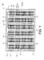
FIG. 1] FIG. 1 is a plan view of a solar cell module according to an embodiment of the present invention, as observed from a light-receiving surface side. - [
FIG. 2] FIG. 2 is a sectional view taken along an A-A line inFIG. 1 . - [
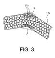
FIG. 3] FIG. 3 is a view illustrating a sectional observation state of an end portion of a wiring material of the solar cell module according to the embodiment of the present invention. - [
FIG. 4] FIG. 4 is a view illustrating a state where the wiring material of the solar cell module according to the embodiment of the present invention is cut. - [
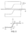
FIG. 5] FIG. 5 is a view illustrating a state where the wiring material of the solar cell module according to the embodiment of the present invention is pressed. - [
FIG. 6] FIG. 6 is a view illustrating a state where the wiring materials of the solar cell module according to the embodiment of the present invention are connected to a solar cell. - [
FIG. 7] FIG. 7 is a sectional view of a solar cell module according to a modified example of the embodiment of the present invention. - [
FIG. 8] FIG. 8 is a view illustrating a state where a wiring material of the solar cell module according to the modified example of the embodiment of the present invention is cut. - [
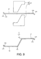
FIG. 9] FIG. 9 is a view illustrating a state where the wiring material of the solar cell module according to the modified example of the embodiment of the present invention is pressed. - [
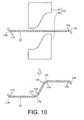
FIG. 10] FIG. 10 is a view illustrating a state where the wiring material of the solar cell module according to the modified example of the embodiment of the present invention is pressed. - As illustrated in
FIG. 1 andFIG. 2 , asolar cell module 10 includes: a plurality ofsolar cells 11;wiring materials 17 that connect thesolar cells 11 to each other;crossover wiring materials 18 that connect thewiring materials 17 to each other;output wiring materials 19 for taking an output to the outside; a first protectingmember 12 placed on a light-receiving surface side of thesolar cells 11; a second protectingmember 13 placed on a rear surface side of thesolar cells 11; afilling material 14 that fills a space between thesolar cells 11 and the first protectingmember 12 and a space between thesolar cells 11 and the second protectingmember 13; and aframe 20 attached to end portions of the first protectingmember 12 and the second protectingmember 13. - The "light-receiving surface" is one of the main surfaces of each
solar cell 11, and refers to a surface through which light from the outside mainly enters. For example, 50% to 100% of the light that enters eachsolar cell 11 enters from the light-receiving surface side. The "rear surface" is one of the main surfaces of eachsolar cell 11, and refers to a surface opposite the light-receiving surface. - A transparent plate or film (for example, a translucent member such as a glass plate, a resin plate, or a resin film) can be used for the first protecting
member 12. Similar to the case of the first protectingmember 12, a glass plate, a resin plate, a resin film, or the like can be used for the second protectingmember 13. Note that, in the case where light reception from the rear surface side is not assumed, an opaque plate or film may be used for the second protectingmember 13, and, for example, a laminate film such as a resin film having aluminum foil therein may be used therefor. - Each
solar cell 11 includes: aphotoelectric conversion section 21 that receives light such as sunlight to thereby generate carriers (electrons and holes); a light-receivingsurface electrode 22 provided on a light-receiving surface of thephotoelectric conversion section 21; and a rear surface electrode 23 provided on a rear surface of thephotoelectric conversion section 21. In thesolar cell 11, the carriers generated by thephotoelectric conversion section 21 are collected by the light-receivingsurface electrode 22 and the rear surface electrode 23. The light-receivingsurface electrode 22 and the rear surface electrode 23 are made of metal. Note that, in order to reduce a light shielding loss, preferably, the light-receivingsurface electrode 22 is smaller in area than the rear surface electrode 23. - The
photoelectric conversion section 21 includes, for example, a substrate made of a semiconductor material such as crystalline silicon, gallium arsenide (GaAs), or indium phosphide (InP). No particular limitation is imposed on the structure of thephotoelectric conversion section 21, and in the present embodiment the structure is described as having a heterojunction between an n-type single-crystal silicon substrate and amorphous silicon. In thephotoelectric conversion section 21, for example, an i-type amorphous silicon layer, a p-type amorphous silicon layer doped with boron (B) and the like, and a transparent conductive layer made of a translucent conductive oxide such as indium oxide are laminated in the stated order on a light-receiving surface of the n-type single-crystal silicon substrate. Further, an i-type amorphous silicon layer, an n-type amorphous silicon layer doped with phosphorus (P) and the like, and a transparent conductive layer are laminated in the stated order on a rear surface of the substrate. - The light-receiving
surface electrode 22 includes a plurality of (for example, 50) finger sections 24 and a plurality of (for example, 2)bus bar sections 25. - The finger sections 24 and the
bus bar sections 25 are placed so as to intersect with each other, and are electrically connected to each other. The finger sections 24 and thebus bar sections 25 are formed by, for example, screen-printing a desired pattern on the transparent conductive layer using a conductive paste in which a conductive filler of silver (Ag) and the like is dispersed in a binder resin. - The finger sections 24 are electrodes that collect carriers evenly across the entire
photoelectric conversion section 21. The finger sections 24 are placed so as to be parallel to each other with a predetermined interval (for example, 1.5 mm to 3 mm) over substantially the entire light-receiving surface. The width of each finger section 24 is preferably about 50 µm to 150 µm, and the thickness thereof is preferably about 20 µm to 80 µm. - The
bus bar sections 25 are connection electrodes to which thewiring materials 17 are respectively electrically connected with the intermediation of anadhesive layer 27. For example, metal such as copper can be used for thewiring materials 17. For example, a thermosetting adhesive containing an adhesive resin material such as epoxy resin, acrylic resin, or urethane resin can be used for theadhesive layer 27. Further, for example, an anisotropic conductive adhesive in which conductive particles are uniformly dispersed in an adhesive having high insulation properties can also be used for theadhesive layer 27. - The
bus bar sections 25 are placed so as to be parallel to each other with a predetermined interval. Thebus bar sections 25 mainly serve for power collection of carriers from the finger sections 24 and transmission thereof to thewiring materials 17. The width of eachbus bar section 25 is preferably about 1.5 mm to 3 mm, and the thickness thereof is preferably about 20 µm to 160 µm. - Similar to the light-receiving
surface electrode 22, the rear surface electrode 23 includes a plurality of finger sections (not illustrated) and a plurality of bus bar sections 26 (connection electrodes). The number of the finger sections of the rear surface electrode 23 may be set to be larger than the number of the finger sections 24, and the interval thereof may be set to be smaller than the interval of the finger sections 24 (for example, number: 250 and interval: 0.5 mm). Note that, in the case where light reception from the rear surface side is not assumed, the rear surface electrode 23 may be obtained by forming a metal film such as a silver (Ag) thin film over the entire rear surface of thephotoelectric conversion section 21. - Next, a connection relation between the
wiring materials 17 and thesolar cells 11 and the like is described in detail. - As illustrated in
FIG. 2 , two adjacentsolar cells 11 are electrically connected to each other by thewiring materials 17. Thewiring materials 17 are placed along the arrangement of thesolar cells 11. Thewiring materials 17 are respectively joined to: thebus bar sections 25 formed on the light-receiving surface of onesolar cell 11; and thebus bar sections 26 formed on the rear surface of the othersolar cell 11, by means of theadhesive layers 27. As a result, thebus bar sections 25 and thebus bar sections 26 are electrically connected to each other. - The
wiring materials 17 are respectively connected to thebus bar sections adhesive layers 27, and are bent, at regions in contact with theadhesive layers 27, to thebus bar section bent portions 17a to 17d toward end portions of theadhesive layers 27. The "bent portions" refer to folds that are formed in eachwiring material 17 by press working or wiring material cutting to be described later. - Each
wiring material 17 is provided so as to be laid between aboundary portion 17i on the light-receiving surface of the onesolar cell 11 and aboundary portion 17j on the rear surface of the othersolar cell 11. The "boundary portions" refer to folds that are formed by press working to be described later such that thewiring material 17 can be laid between the light-receiving surface of the onesolar cell 11 and the rear surface of the othersolar cell 11 located on the opposite side. Thebent portions 17a to 17d are provided on the end portion sides of thewiring material 17 with respect to theboundary portions bent portions wiring material 17. Thebent portions boundary portions wiring material 17. - Each
wiring material 17 includesinclined portions 17e to 17h that are portions that respectively extend from thebent portions 17a to 17d toward the end portions of the adhesive layers 27. Theinclined portions 17e to 17h are respectively inclined from thebent portions 17a to 17d to thebus bar section inclined portions 17e to 17h is preferably about 10% to 20% (for example, 1 cm to 2 cm) of the length along the extending direction of thewiring material 17, of the plane of thephotoelectric conversion section 21. - As illustrated in
FIG. 3 , if a section of the wiring material 17 (representatively, thebent portion 17a) is observed using, for example, a scanning electron microscope (SEM), the particle diameters of metal atoms are smaller in an outer region B and an inner region C than in the remaining regions. That is, the crystal density is higher in the outer region B and the inner region C than in the remaining regions. For example, the crystal density is higher by 30% to 50% in the outer region B and the inner region C than in the remaining regions. Thebent portions 17b to 17d each have a sectional structure similar to that of thebent portion 17a. - Next, a method for manufacturing the
solar cell module 10 is described. - First, as illustrated in
FIG. 4 , thewiring material 17 is fixed from above and below bychuck devices 28, and thewiring material 17 is cut from above and below by acutter 29. - Subsequently, as illustrated in an upper part of
FIG. 5 , thecut wiring material 17 is fitted into a die 30 to be pressed. Consequently, as illustrated in a lower part ofFIG. 5 , thewiring material 17 that is bent so as to follow the shape of the die 30 is formed. The die 30 includes a pair of afirst die section 31 and a second die section 32 having concave and convex portions that are necessary to bend thewiring material 17 at thebent portions 17a to 17d and thus form theinclined portions 17e to 17h. - Subsequently, the
adhesive layers 27 are respectively formed on thebus bar sections 25 and thebus bar sections 26 of two adjacentsolar cells 11, and thewiring materials 17 are placed thereon. At this time, thewiring materials 17 are placed in a state where thewiring materials 17 are bent, at the regions in contact with theadhesive layers 27, to thebus bar section bent portions 17a to 17d toward the end portions of the adhesive layers 27. Specifically, thewiring materials 17 are placed such that: theinclined portions adhesive layer 27 on thebus bar sections 25; and theinclined portions adhesive layer 27 on thebus bar sections 26. - Subsequently, as illustrated in
FIG. 6 , heating is performed in a state where aheating device 36 is compression-bonded to thewiring materials 17 from above and below, whereby theadhesive layers 27 are thermally cured to connect thewiring materials 17 and thesolar cell 11. Theheating device 36 includes aflexible sheet material 34 made of a silicone resin and the like and aheater 35. Thewiring materials 17 are placed in the state where thewiring materials 17 are bent, at the regions in contact with theadhesive layers 27 on thebus bar sections bus bar section wiring materials 17 are firmly joined to thebus bar sections inclined portions 17e to 17h. Accordingly, even when theheating device 36 is separated from thewiring materials 17 after the end of the thermal compression bonding by theheating device 36, thewiring materials 17 can be prevented from coming off thebus bar sections - The present invention includes various embodiments that are not described herein.
- For example, the
wiring materials 17 do not necessarily need to be bent at all thebent portions 17a to 17d, and may be bent at only part(s) thereof. Specifically, as illustrated inFIG. 7 , in asolar cell module 10a, thewiring materials 17 are not bent at portions corresponding to thebent portions solar cell module 10, thewiring materials 17 are respectively connected to thebus bar sections adhesive layers 27, and are bent, at the regions in contact with theadhesive layers 27, to thebus bar section bent portions solar cell module 10a, theinclined portions wiring material 17 are inclined to thebus bar section - Further, the
wiring materials 17 do not necessarily need to be bent by the die 30 at all thebent portions 17a to 17d. For example, in the step of cutting eachwiring material 17, thewiring material 17 may be bent at thebent portions FIG. 8 , the positions of thechuck devices 28 are shifted with respect to each other in the top-bottom direction, thewiring material 17 is fixed to thechuck devices 28, and thewiring material 17 is cut from above and below by thecutter 29. Consequently, in this stage, thewiring material 17 is bent at thebent portions inclined portions - With the use of the
wiring material 17 that is bent at thebent portions FIG. 9 , thecut wiring material 17 is fitted into a die 37 to be pressed. Thedie 37 includes a pair of afirst die section 38 and asecond die section 39 having concave and convex portions for forming a bent shape that is necessary to lay thewiring material 17 between eachbus bar section 25 and eachbus bar section 26. Unlike the die 30, thedie 37 does not have such concave and convex portions that bend thewiring material 17 at thebent portions wiring material 17 is pressed using thedie 37 thus configured. Consequently, as illustrated in a lower part ofFIG. 9 , thewiring material 17 that is bent so as to follow the concave and convex portions of the die 37 is formed. - Further, even in the case of using the
wiring material 17 bent at thebent portions FIG. 10 , thewiring material 17 may be pressed using a die 40 including a pair of a first die section 41 and a second die section 42 having concave and convex portions that are necessary to bend thewiring material 17 at thebent portions inclined portions FIG. 10 , thewiring material 17 in which not only theinclined portions inclined portions - 10, 10a solar cell module, 11 solar cell, 12 first protecting member, 13 second protecting member, 14 filling material, 17 wiring material, 17a, 17b, 17c, 17d bent portion, 17i, 17j boundary portion, 18 crossover wiring material, 19 output wiring material, 20 frame, 21 photoelectric conversion section, 22 light-receiving surface electrode, 23 rear surface electrode, 24 finger section, 25, 26 bus bar section, 27 adhesive layer, 28 chuck device, 29 cutter, 30, 37, 40 die, 31, 38, 41 first die section, 32, 39, 42 second die section, 34 sheet material, 35 heater
Claims (7)
- A solar cell module comprising:solar cells each including a connection electrode on a main surface thereof;an adhesive layer provided on each connection electrode; anda wiring material that is connected to each connection electrode by means of the adhesive layer and is bent, at regions in contact with the adhesive layer, to the connection electrode side from bent portions toward end portions of the adhesive layer.
- The solar cell module according to claim 1, wherein the bent portions are respectively provided in vicinities of end portions of the wiring material.
- The solar cell module according to claim 1 or claim 2, wherein
the wiring material is provided so as to be laid between a boundary portion on a light-receiving surface of one solar cell and a boundary portion on a rear surface of another solar cell, and
the bent portions are respectively provided on the end portion sides of the wiring material with respect to the boundary portions. - The solar cell module according to claim 3, wherein the bent portions are respectively provided in vicinities of the boundary portions.
- A method for manufacturing a solar cell module comprising:providing an adhesive layer on a connection electrode provided on a main surface of each of solar cells; andconnecting, when a wiring material is connected to the connection electrode by means of the adhesive layer, the wiring material to the adhesive layer in a state where the wiring material is bent, at regions in contact with the adhesive layer, to the connection electrode side from bent portions toward end portions of the adhesive layer.
- The method for manufacturing a solar cell module according to claim 5, wherein the bent wiring material is formed by press working.
- The method for manufacturing a solar cell module according to claim 5, wherein the bent wiring material is formed by cutting the wiring material.
Applications Claiming Priority (1)
| Application Number | Priority Date | Filing Date | Title |
|---|---|---|---|
| PCT/JP2012/052094 WO2013114555A1 (en) | 2012-01-31 | 2012-01-31 | Solar cell module, and method for manufacturing solar cell module |
Publications (2)
| Publication Number | Publication Date |
|---|---|
| EP2811532A1 true EP2811532A1 (en) | 2014-12-10 |
| EP2811532A4 EP2811532A4 (en) | 2015-07-01 |
Family
ID=48904635
Family Applications (1)
| Application Number | Title | Priority Date | Filing Date |
|---|---|---|---|
| EP12867704.4A Withdrawn EP2811532A4 (en) | 2012-01-31 | 2012-01-31 | SOLAR CELL MODULE AND METHOD FOR MANUFACTURING SOLAR CELL MODULE |
Country Status (4)
| Country | Link |
|---|---|
| US (1) | US20140190547A1 (en) |
| EP (1) | EP2811532A4 (en) |
| CN (1) | CN103782396A (en) |
| WO (1) | WO2013114555A1 (en) |
Families Citing this family (5)
| Publication number | Priority date | Publication date | Assignee | Title |
|---|---|---|---|---|
| WO2014208312A1 (en) * | 2013-06-28 | 2014-12-31 | 三洋電機株式会社 | Solar battery cell module and method of manufacturing same |
| CN105449020B (en) * | 2014-08-29 | 2018-01-23 | 英属开曼群岛商精曜有限公司 | Solar components and solar cell |
| KR20160038694A (en) * | 2014-09-30 | 2016-04-07 | 엘지전자 주식회사 | Solar cell and solar cell panel including the same |
| TWI609499B (en) * | 2016-07-01 | 2017-12-21 | 錸德科技股份有限公司 | Solar cell module and manufacturing method thereof |
| KR20250129380A (en) * | 2024-02-22 | 2025-08-29 | 한화솔루션 주식회사 | Bending apparatus and tabbing apparatus including the same |
Family Cites Families (9)
| Publication number | Priority date | Publication date | Assignee | Title |
|---|---|---|---|---|
| US20050115602A1 (en) * | 2003-11-28 | 2005-06-02 | Kyocera Corporation | Photo-electric conversion cell and array, and photo-electric generation system |
| JP4738147B2 (en) * | 2005-03-29 | 2011-08-03 | 京セラ株式会社 | Solar cell module and manufacturing method thereof |
| JP5323310B2 (en) * | 2005-11-10 | 2013-10-23 | 日立化成株式会社 | Connection structure and manufacturing method thereof |
| KR101267181B1 (en) * | 2006-01-31 | 2013-05-23 | 산요덴키가부시키가이샤 | Solar cell elements and solar modules |
| TWI438916B (en) * | 2007-07-13 | 2014-05-21 | Sanyo Electric Co | Solar cell module manufacturing method |
| WO2009041506A1 (en) * | 2007-09-26 | 2009-04-02 | Hitachi Chemical Company, Ltd. | Member for conductor connection, method for manufacturing the same, connection structure, and solar cell module |
| JP5147672B2 (en) * | 2008-01-31 | 2013-02-20 | 三洋電機株式会社 | Solar cell module and method for manufacturing solar cell module |
| JP5436901B2 (en) * | 2009-03-23 | 2014-03-05 | 三洋電機株式会社 | Manufacturing method of solar cell module |
| JP5759220B2 (en) * | 2011-03-29 | 2015-08-05 | デクセリアルズ株式会社 | Solar cell module and method for manufacturing solar cell module |
-
2012
- 2012-01-31 WO PCT/JP2012/052094 patent/WO2013114555A1/en not_active Ceased
- 2012-01-31 EP EP12867704.4A patent/EP2811532A4/en not_active Withdrawn
- 2012-01-31 CN CN201280043896.0A patent/CN103782396A/en active Pending
-
2014
- 2014-03-10 US US14/202,586 patent/US20140190547A1/en not_active Abandoned
Also Published As
| Publication number | Publication date |
|---|---|
| WO2013114555A1 (en) | 2013-08-08 |
| CN103782396A (en) | 2014-05-07 |
| US20140190547A1 (en) | 2014-07-10 |
| EP2811532A4 (en) | 2015-07-01 |
Similar Documents
| Publication | Publication Date | Title |
|---|---|---|
| JP5288790B2 (en) | Solar cell module and manufacturing method thereof | |
| JP6586080B2 (en) | Solar cell module and manufacturing method thereof | |
| JP5279334B2 (en) | Solar cell module | |
| JP2009081197A (en) | Method for manufacturing solar cell module and solar cell module | |
| JP4948219B2 (en) | Solar cell | |
| CN102132419B (en) | Photoelectric conversion cell and photoelectric conversion module | |
| JP2008235521A (en) | Semiconductor substrate cleaving method, solar cell cleaving method, and solar cell | |
| EP2043164A2 (en) | Solar cell module | |
| EP2393122B1 (en) | Photoelectric conversion cell, photoelectric conversion module, and method for manufacturing photoelectric conversion cell | |
| US20140190547A1 (en) | Solar cell module, and method for manufacturing solar cell module | |
| KR101605132B1 (en) | Solar battery module and method for manufacturing same | |
| EP2418686A1 (en) | Solar cell and solar cell module | |
| JP2011159676A (en) | Solar cell device, and solar cell module using the same | |
| JP5362201B2 (en) | Solar cell module | |
| CN104221160B (en) | Solar module and manufacture method thereof | |
| JP5617853B2 (en) | Solar cell module | |
| JP5381809B2 (en) | Solar cell module | |
| JP6467727B2 (en) | Manufacturing method of solar cell module | |
| US10147831B2 (en) | Solar module and manufacturing method therefor | |
| CN104221161A (en) | Solar cell module and solar cell module manufacturing method | |
| JP2011044751A (en) | Solar cell module | |
| JP5100216B2 (en) | Solar cell group and manufacturing method thereof, solar cell module including solar cell group and manufacturing method thereof | |
| JP2018056490A (en) | Solar cell module and solar cell | |
| JP6019417B2 (en) | Semiconductor substrate cleaving method, solar cell cleaving method, and solar cell | |
| JPWO2013114555A1 (en) | Solar cell module and method for manufacturing solar cell module |
Legal Events
| Date | Code | Title | Description |
|---|---|---|---|
| PUAI | Public reference made under article 153(3) epc to a published international application that has entered the european phase |
Free format text: ORIGINAL CODE: 0009012 |
|
| 17P | Request for examination filed |
Effective date: 20140307 |
|
| AK | Designated contracting states |
Kind code of ref document: A1 Designated state(s): AL AT BE BG CH CY CZ DE DK EE ES FI FR GB GR HR HU IE IS IT LI LT LU LV MC MK MT NL NO PL PT RO RS SE SI SK SM TR |
|
| AX | Request for extension of the european patent |
Extension state: BA ME |
|
| DAX | Request for extension of the european patent (deleted) | ||
| RA4 | Supplementary search report drawn up and despatched (corrected) |
Effective date: 20150601 |
|
| RIC1 | Information provided on ipc code assigned before grant |
Ipc: H01L 31/05 20140101AFI20150526BHEP |
|
| STAA | Information on the status of an ep patent application or granted ep patent |
Free format text: STATUS: THE APPLICATION HAS BEEN WITHDRAWN |
|
| RAP1 | Party data changed (applicant data changed or rights of an application transferred) |
Owner name: PANASONIC INTELLECTUAL PROPERTY MANAGEMENT CO., LT |
|
| 18W | Application withdrawn |
Effective date: 20151105 |