EP2811518A2 - Semiconductor device - Google Patents
Semiconductor device Download PDFInfo
- Publication number
- EP2811518A2 EP2811518A2 EP20140155485 EP14155485A EP2811518A2 EP 2811518 A2 EP2811518 A2 EP 2811518A2 EP 20140155485 EP20140155485 EP 20140155485 EP 14155485 A EP14155485 A EP 14155485A EP 2811518 A2 EP2811518 A2 EP 2811518A2
- Authority
- EP
- European Patent Office
- Prior art keywords
- transistor
- normally
- source
- drain
- gate
- Prior art date
- Legal status (The legal status is an assumption and is not a legal conclusion. Google has not performed a legal analysis and makes no representation as to the accuracy of the status listed.)
- Granted
Links
Images


Classifications
-
- H—ELECTRICITY
- H10—SEMICONDUCTOR DEVICES; ELECTRIC SOLID-STATE DEVICES NOT OTHERWISE PROVIDED FOR
- H10D—INORGANIC ELECTRIC SEMICONDUCTOR DEVICES
- H10D89/00—Aspects of integrated devices not covered by groups H10D84/00 - H10D88/00
- H10D89/60—Integrated devices comprising arrangements for electrical or thermal protection, e.g. protection circuits against electrostatic discharge [ESD]
- H10D89/601—Integrated devices comprising arrangements for electrical or thermal protection, e.g. protection circuits against electrostatic discharge [ESD] for devices having insulated gate electrodes, e.g. for IGFETs or IGBTs
- H10D89/611—Integrated devices comprising arrangements for electrical or thermal protection, e.g. protection circuits against electrostatic discharge [ESD] for devices having insulated gate electrodes, e.g. for IGFETs or IGBTs using diodes as protective elements
-
- H—ELECTRICITY
- H03—ELECTRONIC CIRCUITRY
- H03K—PULSE TECHNIQUE
- H03K17/00—Electronic switching or gating, i.e. not by contact-making and –breaking
- H03K17/51—Electronic switching or gating, i.e. not by contact-making and –breaking characterised by the components used
- H03K17/56—Electronic switching or gating, i.e. not by contact-making and –breaking characterised by the components used by the use, as active elements, of semiconductor devices
- H03K17/567—Circuits characterised by the use of more than one type of semiconductor device, e.g. BIMOS, composite devices such as IGBT
-
- H—ELECTRICITY
- H10—SEMICONDUCTOR DEVICES; ELECTRIC SOLID-STATE DEVICES NOT OTHERWISE PROVIDED FOR
- H10D—INORGANIC ELECTRIC SEMICONDUCTOR DEVICES
- H10D89/00—Aspects of integrated devices not covered by groups H10D84/00 - H10D88/00
- H10D89/60—Integrated devices comprising arrangements for electrical or thermal protection, e.g. protection circuits against electrostatic discharge [ESD]
- H10D89/601—Integrated devices comprising arrangements for electrical or thermal protection, e.g. protection circuits against electrostatic discharge [ESD] for devices having insulated gate electrodes, e.g. for IGFETs or IGBTs
- H10D89/811—Integrated devices comprising arrangements for electrical or thermal protection, e.g. protection circuits against electrostatic discharge [ESD] for devices having insulated gate electrodes, e.g. for IGFETs or IGBTs using FETs as protective elements
-
- H—ELECTRICITY
- H10—SEMICONDUCTOR DEVICES; ELECTRIC SOLID-STATE DEVICES NOT OTHERWISE PROVIDED FOR
- H10W—GENERIC PACKAGES, INTERCONNECTIONS, CONNECTORS OR OTHER CONSTRUCTIONAL DETAILS OF DEVICES COVERED BY CLASS H10
- H10W90/00—Package configurations
-
- H—ELECTRICITY
- H10—SEMICONDUCTOR DEVICES; ELECTRIC SOLID-STATE DEVICES NOT OTHERWISE PROVIDED FOR
- H10D—INORGANIC ELECTRIC SEMICONDUCTOR DEVICES
- H10D84/00—Integrated devices formed in or on semiconductor substrates that comprise only semiconducting layers, e.g. on Si wafers or on GaAs-on-Si wafers
- H10D84/80—Integrated devices formed in or on semiconductor substrates that comprise only semiconducting layers, e.g. on Si wafers or on GaAs-on-Si wafers characterised by the integration of at least one component covered by groups H10D12/00 or H10D30/00, e.g. integration of IGFETs
- H10D84/811—Combinations of field-effect devices and one or more diodes, capacitors or resistors
-
- H—ELECTRICITY
- H10—SEMICONDUCTOR DEVICES; ELECTRIC SOLID-STATE DEVICES NOT OTHERWISE PROVIDED FOR
- H10D—INORGANIC ELECTRIC SEMICONDUCTOR DEVICES
- H10D84/00—Integrated devices formed in or on semiconductor substrates that comprise only semiconducting layers, e.g. on Si wafers or on GaAs-on-Si wafers
- H10D84/80—Integrated devices formed in or on semiconductor substrates that comprise only semiconducting layers, e.g. on Si wafers or on GaAs-on-Si wafers characterised by the integration of at least one component covered by groups H10D12/00 or H10D30/00, e.g. integration of IGFETs
- H10D84/82—Integrated devices formed in or on semiconductor substrates that comprise only semiconducting layers, e.g. on Si wafers or on GaAs-on-Si wafers characterised by the integration of at least one component covered by groups H10D12/00 or H10D30/00, e.g. integration of IGFETs of only field-effect components
-
- H—ELECTRICITY
- H10—SEMICONDUCTOR DEVICES; ELECTRIC SOLID-STATE DEVICES NOT OTHERWISE PROVIDED FOR
- H10W—GENERIC PACKAGES, INTERCONNECTIONS, CONNECTORS OR OTHER CONSTRUCTIONAL DETAILS OF DEVICES COVERED BY CLASS H10
- H10W72/00—Interconnections or connectors in packages
- H10W72/50—Bond wires
- H10W72/531—Shapes of wire connectors
- H10W72/536—Shapes of wire connectors the connected ends being ball-shaped
-
- H—ELECTRICITY
- H10—SEMICONDUCTOR DEVICES; ELECTRIC SOLID-STATE DEVICES NOT OTHERWISE PROVIDED FOR
- H10W—GENERIC PACKAGES, INTERCONNECTIONS, CONNECTORS OR OTHER CONSTRUCTIONAL DETAILS OF DEVICES COVERED BY CLASS H10
- H10W72/00—Interconnections or connectors in packages
- H10W72/50—Bond wires
- H10W72/541—Dispositions of bond wires
- H10W72/5449—Dispositions of bond wires not being orthogonal to a side surface of the chip, e.g. fan-out arrangements
-
- H—ELECTRICITY
- H10—SEMICONDUCTOR DEVICES; ELECTRIC SOLID-STATE DEVICES NOT OTHERWISE PROVIDED FOR
- H10W—GENERIC PACKAGES, INTERCONNECTIONS, CONNECTORS OR OTHER CONSTRUCTIONAL DETAILS OF DEVICES COVERED BY CLASS H10
- H10W72/00—Interconnections or connectors in packages
- H10W72/90—Bond pads, in general
- H10W72/921—Structures or relative sizes of bond pads
- H10W72/926—Multiple bond pads having different sizes
-
- H—ELECTRICITY
- H10—SEMICONDUCTOR DEVICES; ELECTRIC SOLID-STATE DEVICES NOT OTHERWISE PROVIDED FOR
- H10W—GENERIC PACKAGES, INTERCONNECTIONS, CONNECTORS OR OTHER CONSTRUCTIONAL DETAILS OF DEVICES COVERED BY CLASS H10
- H10W90/00—Package configurations
- H10W90/701—Package configurations characterised by the relative positions of pads or connectors relative to package parts
- H10W90/731—Package configurations characterised by the relative positions of pads or connectors relative to package parts of die-attach connectors
- H10W90/732—Package configurations characterised by the relative positions of pads or connectors relative to package parts of die-attach connectors between stacked chips
-
- H—ELECTRICITY
- H10—SEMICONDUCTOR DEVICES; ELECTRIC SOLID-STATE DEVICES NOT OTHERWISE PROVIDED FOR
- H10W—GENERIC PACKAGES, INTERCONNECTIONS, CONNECTORS OR OTHER CONSTRUCTIONAL DETAILS OF DEVICES COVERED BY CLASS H10
- H10W90/00—Package configurations
- H10W90/701—Package configurations characterised by the relative positions of pads or connectors relative to package parts
- H10W90/751—Package configurations characterised by the relative positions of pads or connectors relative to package parts of bond wires
- H10W90/752—Package configurations characterised by the relative positions of pads or connectors relative to package parts of bond wires between stacked chips
-
- H—ELECTRICITY
- H10—SEMICONDUCTOR DEVICES; ELECTRIC SOLID-STATE DEVICES NOT OTHERWISE PROVIDED FOR
- H10W—GENERIC PACKAGES, INTERCONNECTIONS, CONNECTORS OR OTHER CONSTRUCTIONAL DETAILS OF DEVICES COVERED BY CLASS H10
- H10W90/00—Package configurations
- H10W90/701—Package configurations characterised by the relative positions of pads or connectors relative to package parts
- H10W90/751—Package configurations characterised by the relative positions of pads or connectors relative to package parts of bond wires
- H10W90/753—Package configurations characterised by the relative positions of pads or connectors relative to package parts of bond wires between laterally-adjacent chips
-
- H—ELECTRICITY
- H10—SEMICONDUCTOR DEVICES; ELECTRIC SOLID-STATE DEVICES NOT OTHERWISE PROVIDED FOR
- H10W—GENERIC PACKAGES, INTERCONNECTIONS, CONNECTORS OR OTHER CONSTRUCTIONAL DETAILS OF DEVICES COVERED BY CLASS H10
- H10W90/00—Package configurations
- H10W90/701—Package configurations characterised by the relative positions of pads or connectors relative to package parts
- H10W90/751—Package configurations characterised by the relative positions of pads or connectors relative to package parts of bond wires
- H10W90/756—Package configurations characterised by the relative positions of pads or connectors relative to package parts of bond wires between a chip and a stacked lead frame, conducting package substrate or heat sink
Definitions
- Embodiments described herein relate generally to a semiconductor device.
- a group-III nitride semiconductor for example, a GaN (gallium nitride)-based semiconductor is expected as a material of a next-generation power semiconductor device.
- a GaN-based semiconductor device has a band gap wider than that of a Si (silicon) semiconductor and this may realize higher withstand voltage and lower loss than those of the Si semiconductor device.
- a HEMT high electron mobility transistor
- 2DEG two-dimensional electron gas
- a semiconductor device of an embodiment is provided with a normally-off transistor including a first source connected to a source terminal, a first drain, and a first gate connected to a gate terminal and a normally-on transistor including a second source connected to the first drain, a second drain connected to a drain terminal, and a second gate connected to the source terminal.
- a withstand voltage between the first source and the first drain when the normally-off transistor is turned off is lower than a withstand voltage between the second source and the second gate of the normally-on transistor.
- the semiconductor device is a concept including a power module in which a plurality of devices such as a discrete semiconductor are combined, an intelligent power module in which a driver circuit which drives the devices and a self-protection function are incorporated in a plurality of devices such as the discrete semiconductor, or an entire system provided with the power module and the intelligent power module.
- a semiconductor device of this embodiment is provided with a source terminal, a drain terminal, a gate terminal, a normally-off transistor including a first source connected to the source terminal, a first drain, and a first gate connected to the gate terminal, and a normally-on transistor including a second source connected to the first drain, a second drain connected to the drain terminal, and a second gate connected to the source terminal.
- a withstand voltage between the first source and the first drain when the normally-off transistor is turned off is lower than a withstand voltage between the second source and the second gate of the normally-on transistor.
- FIG. 1 is a circuit diagram of the semiconductor device of this embodiment.
- the semiconductor device of this embodiment is a power module having a rated voltage of 600 V or 1200 V, for example.
- a normally-off transistor 10 and a normally-on transistor 20 are cascode connected to form the power module.
- the normally-off transistor 10 is a Si (silicon)-vertical MOSFET (metal oxide semiconductor field effect transistor), for example.
- the normally-on transistor 20 is a GaN (gallium nitride)-based HEMT, for example.
- the normally-on transistor 20 is provided with a gate insulation film.
- the normally-off transistor 10 includes a parasitic body diode not illustrated.
- the normally-off transistor 10 has a device withstand voltage lower than that of the normally-on transistor 20.
- the device withstand voltage of the normally-off transistor 10 is 10 to 30 V, for example.
- the device withstand voltage of the normally-on transistor 20 is 600 to 1200 V, for example.
- the semiconductor device is provided with a source terminal 100, a drain terminal 200, and a gate terminal 300.
- the normally-off transistor 10 includes a first source 11 connected to the source terminal 100, a first drain 12, and a first gate 13 connected to the gate terminal 300.
- the normally-on transistor 20 includes a second source 21 connected to the first drain 12, a second drain 22 connected to the drain terminal 200, and a second gate 23 connected to the source terminal 100.
- the semiconductor device of this embodiment serves as a normally-off transistor provided with the source terminal 100, the drain terminal 200, and the gate terminal 300 by the above-described configuration.
- the withstand voltage between the first source 11 and the first drain 12 when the normally-off transistor 10 is turned off is lower than the withstand voltage between the second source 21 and the second gate 23 of the normally-on transistor 20.
- an avalanche breakdown voltage of the normally-off transistor 10 is designed to be lower than a withstand voltage of the gate insulation film of the normally-on transistor 20.
- the avalanche breakdown voltage of the normally-off transistor 10 is specified by a withstand voltage of the parasitic body diode of the normally-off transistor 10 or a punch-through withstand voltage of a channel unit. It is possible to adjust the avalanche breakdown voltage of the normally-off transistor 10 by adjusting impurity concentration and an impurity profile of an impurity layer forming the normally-off transistor 10, for example.
- an overvoltage might be generated during device operation at a connection between the normally-off transistor 10 and the normally-on transistor 20 (hereinafter, also simply referred to as a connection), that is to say, the first drain 12 of the normally-off transistor 10 or the second source 21 of the normally-on transistor 20.
- the overvoltage might be generated by voltage dividing of a high voltage applied between the source terminal 100 and the drain terminal 200 at a parasitic capacitance ratio between the normally-off transistor 10 and the normally-on transistor 20 when the semiconductor device shifts from an on-state to an off-state, for example.
- this might be generated by the voltage dividing of the high voltage applied between the source terminal 100 and the drain terminal 200 at a leakage current ratio between the normally-off transistor 10 and the normally-on transistor 20 when the semiconductor device is turned off.
- the avalanche breakdown voltage of the normally-off transistor 10 is designed to be lower than the withstand voltage of the gate insulation film of the normally-on transistor 20. According to this, the withstand voltage between the first source and the first drain when the normally-off transistor is turned off is made lower than the withstand voltage between the second source and the second gate of the normally-on transistor.
- the withstand voltage of the gate insulation film of the normally-on transistor 20 is higher than 30 V in general. Therefore, the avalanche breakdown voltage of the normally-off transistor 10 is desirably not higher than 30 V.
- a product of an on-resistance and a rated current of the normally-off transistor 10 is desirably not higher than 2 V. If the product is 2 V or so, it is possible to sufficiently inhibit a decrease in gate bias of the normally-on transistor 20 by a voltage drop occurring in the normally-off transistor 10. Therefore, current loss due to the decrease in the gate bias may be minimized.
- a semiconductor device of this embodiment is different from that of the first embodiment in that a Zener diode including a first anode connected to a first source and a first cathode connected to a first drain and a second source having a Zener voltage lower than an avalanche breakdown voltage of a normally-off transistor is further provided. The description of contents overlapped with those of the first embodiment is not repeated.
- FIG. 2 is a circuit diagram of the semiconductor device of this embodiment.
- a Zener diode 30 is provided in parallel with a normally-off transistor 10.
- the Zener diode 30 includes a first anode 31 and a first cathode 32.
- the first anode 31 is connected to a first source 11.
- the first cathode 32 is connected to a first drain 12 and a second source 21.
- the Zener voltage of the Zener diode 30 is set to be lower than the avalanche breakdown voltage of the normally-off transistor 10.
- the Zener voltage is also set to be lower than a withstand voltage of a gate insulation film of a normally-on transistor 20. According to this, a withstand voltage between the first source 11 and the first drain 12 when the normally-off transistor 10 is turned off becomes lower than a withstand voltage between the second source 21 and a second gate 23 of the normally-on transistor 20.
- the Zener voltage of the Zener diode 30 may be controlled with higher accuracy as compared to the avalanche breakdown voltage of the normally-off transistor 10. Therefore, in the semiconductor device of this embodiment, it becomes possible to inhibit the overvoltage at the connection in a more stable manner than in the first embodiment by using the Zener diode 30. Even when an unexpected high voltage such as noise is applied to the first drain 12 of the normally-off transistor 10, the charge may be released by the Zener diode 30, so that this also contributes to protect the normally-off transistor 10.
- a semiconductor device of this embodiment is different from that of the second embodiment in that a diode including a second anode connected to a first drain and a second source and a second cathode connected to a first cathode provided between the first drain and the second source, and a Zener diode and a capacitor provided between the first cathode and the second cathode, and a first source in parallel with the Zener diode are further provided.
- the description of contents overlapped with those of the second embodiment is not repeated.
- FIG. 3 is a circuit diagram of the semiconductor device of this embodiment.
- a diode 40 is provided on a side of a drain of a normally-off transistor 10.
- a Zener diode 30 is provided in parallel with the normally-off transistor 10.
- a capacitor 50 is provided in parallel with the Zener diode 30.
- the diode 40 is provided between a first drain 12 and a second source 21, and the Zener diode 30.
- the diode 40 includes a second anode 41 and a second cathode 42.
- the second anode is connected to the first drain 12 and the second source 21.
- the second cathode 42 is connected to a first cathode 32.
- the capacitor 50 is provided between the first cathode 32 and the second cathode 42, and a first source 11 in parallel with the Zener diode 30.
- the diode 40 prevents backflow of a charge from a side of the capacitor 50.
- the diode 40 is a PiN diode or a Schottky barrier diode, for example.
- the charge is temporarily accumulated in the capacitor 50. Then, the accumulated charge is released to a side of a source terminal 100 by the Zener diode 30. According to this, an increase in voltage at the connection is inhibited and an increase in leakage current of a gate insulation film of the normally-on transistor 20 and a break of the gate insulation film are prevented. A current collapse is also prevented. Therefore, reliability of the semiconductor device is improved.
- the Zener diode 30 may be an inexpensive diode having a small parasitic capacitance. Therefore, an inexpensive semiconductor device may be realized.
- a capacitance of the capacitor 50 is connected in series to a capacitance of the diode 40 between the first source 11 and the first drain 12 of the normally-off transistor 10.
- a type having a parasitic capacitance significantly smaller than that of the Zener diode 30 may be selected as the diode 40 for a current required for absorbing the charge. Therefore, the capacitance of the capacitor 50 contributes little as a parasitic capacitance of the normally-off transistor 10 by making the capacitance of the diode 40 sufficiently smaller than the capacitance of the capacitor 50. Therefore, a decrease in operation speed of the normally-off transistor 10 and an increase in loss due to an increase in the parasitic capacitance may be inhibited.
- a normally-on transistor includes a gate field plate (hereinafter, also referred to as GFP).
- GFP gate field plate
- Other configuration is similar to that of the first embodiment. Therefore, the description of contents overlapped with those of the first embodiment is not repeated.
- FIG. 4 is a schematic cross-sectional view of the normally-on transistor of this embodiment.
- the normally-on transistor is a GaN (gallium nitride)-based HEMT provided with a gate insulation film.
- a normally-on transistor 20 ( FIG. 1 ) is formed on a nitride semiconductor layer 161 on a substrate 160.
- the substrate 160 is formed of silicon (Si), for example.
- a buffer layer (not illustrated) is provided between the substrate 160 and the nitride semiconductor layer 161.
- the buffer layer serves to reduce lattice mismatch between the substrate 160 and the nitride semiconductor layer 161.
- the buffer layer is formed of a multilayer structure of aluminum gallium nitride (Al x Ga 1-x N (0 ⁇ x ⁇ 1)), for example.
- the nitride semiconductor layer 161 is provided with a laminated structure of an operation layer (channel layer) 161 a and a barrier layer (electron supply layer) 161 b.
- the operation layer 161 a is formed of gallium nitride (GaN), for example, and the barrier layer 161b is formed of aluminum gallium nitride (AlGaN), for example.
- a heterojunction interface is formed between the operation layer 161 a and the barrier layer 161b.
- a gate electrode 164 is formed on the nitride semiconductor layer 161 with a first silicon nitride film 162 interposed therebetween.
- the first silicon nitride film 162 serves as a gate insulation film.
- the gate electrode 164 is, for example, a metal electrode.
- the metal electrode is, for example, a nickel (Ni) electrode, a titanium (Ti) electrode, or an aluminum (Al) electrode.
- a source electrode 166 and a drain electrode 168 are provided on the nitride semiconductor layer 161 with the gate electrode 164 interposed therebetween. Each of the source electrode 166 and the drain electrode 168 is separated from the gate electrode 164.
- a second silicon nitride film 170 is formed between the source electrode 166 and the gate electrode 164 and between the drain electrode 168 and the gate electrode 164 on the nitride semiconductor layer 161.
- the second silicon nitride film 170 is formed so as to be in contact with a surface of the nitride semiconductor layer 161.
- the second silicon nitride film 170 serves as a surface protection film (or a passivation film) which protects the surface of the nitride semiconductor layer 161 between the gate electrode 164 and the source electrode 166 and between the gate electrode 164 and the drain electrode 168.
- the gate electrode 164 extends to a side of the drain electrode 168 on the second silicon nitride film 170.
- a part extended to the drain electrode 168 side of the gate electrode 164 serves as so-called the gate field plate. Meanwhile, a length (d in the drawing) of the part extended to the drain electrode 168 side of the gate electrode 164, that is to say, the part extended to the drain electrode 168 side from a lower end on the drain electrode 168 side of the gate electrode 164 is not shorter than 1 ⁇ m.
- the gate field plate serves to reduce an electric field in a drain region between the gate electrode 164 and the drain electrode 168 to inhibit a current collapse.
- a source field plate (hereinafter, also referred to as SFP) obtained by extending the source electrode 166 to the drain electrode 168 side as a structure to provide a similar function.
- FIG. 5 is a view illustrating parasitic capacitances of the GFP and the SFP.
- a source-drain capacitance (Cds), a source-gate capacitance (Cgs), and a drain-gate capacitance (Cgd) of the GFP and those of the SFP are compared.
- a capacitance simulation result is illustrated.
- a solid line indicates the GFP and a dotted line indicates the SFP.
- the drain-gate capacitance (Cgd) is larger than that in the SFP
- the source-drain capacitance (Cds) and the source-gate capacitance (Cgs) are smaller than those in the SFP.
- the parasitic capacitance of the transistor is desirably small from a viewpoint of avoiding a decrease in operation speed and an increase in loss.
- the drain-gate capacitance (Cgd) has a large effect on parasitic oscillation and a switching speed, so that this is desirably small.
- a second gate 23 of the normally-on transistor 20 is connected to a first source 11 of a normally-off transistor 10 as illustrated in the circuit diagram in FIG. 1 .
- Transistor operation is performed by raising a voltage of a second source 21 of the normally-on transistor 20, so that charge/discharge of the second gate 23 is not directly performed during the operation. Therefore, it is possible to eliminate the effect of the drain-gate capacitance (Cgd) on the operation.
- the GFP having small source-drain capacitance (Cds) and source-gate capacitance (Cgs) is desirable as a structure to realize a reduction in collapse as compared to the SFP.
- the gate electrode itself extends to the drain side is described as an example, a configuration in which a GFP electrode having same potential as the gate electrode is provided on an upper layer and the like of the gate electrode separately from the gate electrode is also possible.
- a semiconductor device of this embodiment is different from the semiconductor device of the second embodiment in that a Schottky barrier diode including a third anode connected to a first source and a third cathode connected to a first drain and a second source having a forward drop voltage lower than a forward drop voltage of a parasitic body diode of a normally-off transistor provided between the first drain and the second source, and the first source in parallel with a Zener diode is further provided.
- a Schottky barrier diode including a third anode connected to a first source and a third cathode connected to a first drain and a second source having a forward drop voltage lower than a forward drop voltage of a parasitic body diode of a normally-off transistor provided between the first drain and the second source, and the first source in parallel with a Zener diode is further provided.
- FIG. 6 is a circuit diagram of the semiconductor device of this embodiment.
- a Zener diode 30 is provided in parallel with a normally-off transistor 10. Further, a Schottky barrier diode 60 is provided in parallel with the Zener diode 30.
- the Schottky barrier diode 60 is provided with a third anode 61 and a third cathode 62.
- the third anode 61 is connected to a first source 11.
- the third cathode 62 is connected to a first drain 12 and a second source 21.
- a forward drop voltage (Vf) of the Schottky barrier diode 60 is lower than a forward drop voltage (Vf) of the parasitic body diode (not illustrated) of the normally-off transistor.
- the Schottky barrier diode 60 is provided between the first drain 12 and the second source 21, and the first source 11 in parallel with the Zener diode 30.
- the Schottky barrier diode 60 When the Schottky barrier diode 60 is not provided, a current flows through the parasitic body diode of the normally-off transistor 10 in a reflux mode in which a source terminal 100 has a positive voltage relative to a drain terminal 200.
- the Schottky barrier diode 60 having the forward drop voltage (Vf) lower than the forward drop voltage (Vf) of the parasitic body diode of the normally-off transistor 10 is provided. According to this, the current flows through the Schottky barrier diode 60 in the reflux mode.
- the Schottky barrier diode operates by using only a majority carrier. Therefore, this is excellent in recovery property as compared to the PiN diode. Therefore, in addition to the effects of the first and second embodiments, it becomes possible to improve the recovery property in the reflux mode in this embodiment. Therefore, the semiconductor device excellent in reliability and recovery property may be realized.
- a normally-on transistor 20 bears a large part of a withstand voltage, so that a low withstand voltage type may be selected as the Schottky barrier diode 60. According to this, it is possible to realize high withstand voltage body diode operation with a Vf property and the recovery property similar to those of the low withstand voltage type.
- Vf forward drop voltage
- the withstand voltage of the Schottky barrier diode 60 is desirably higher than an avalanche breakdown voltage of the normally-off transistor 10.
- a semiconductor device of this embodiment is further provided with a substrate, a source lead wire, a drain lead wire, and a gate lead wire.
- a normally-off transistor, a normally-on transistor, a Zener diode, and a Schottky barrier diode are mounted on the substrate.
- the Schottky barrier diode, the Zener diode, and the normally-on transistor are arranged in this order from a side of the source lead wire to a side of the drain lead wire.
- the normally-off transistor and the normally-on transistor are arranged in this order from the side of the source lead wire to the side of the drain lead wire.
- the source lead wire is connected to a third anode and a first source and the drain lead wire is connected to a second drain.
- This embodiment is obtained by embodying the circuit configuration of the fifth embodiment as a power module. Hereinafter, the description of contents overlapped with those of the fifth embodiment is not repeated.
- FIG. 7 is a top schematic view of the semiconductor device of this embodiment.
- the semiconductor device of this embodiment is provided with a substrate 90, a source lead wire 91, a drain lead wire 92, and a gate lead wire 93.
- the source lead wire 91, the drain lead wire 92, and the gate lead wire 93 correspond to a source terminal 100, a drain terminal 200, and a gate terminal 300, respectively.
- a metal conductive material 95 is present on at least a surface of the substrate 90.
- a normally-off transistor 10, a normally-on transistor 20, a Zener diode 30, and a Schottky barrier diode 60 are mounted on the substrate 90.
- Each of the normally-off transistor 10, the normally-on transistor 20, the Zener diode 30, and the Schottky barrier diode 60 is a semiconductor chip, for example, and is mounted on the conductive material 95 of the substrate with conductive paste and soldering, for example.
- the Schottky barrier diode 60, the Zener diode 30, and the normally-on transistor 20 are arranged in this order from a side of the source lead wire 91 to a side of the drain lead wire 92.
- the normally-off transistor 10 and the normally-on transistor 20 are arranged in this order from the side of the source lead wire 91 to the side of the drain lead wire 92 on the substrate 90.
- the source lead wire 91 is connected to a third anode 61 and a first source 11 and the drain lead wire 92 is connected to a second drain 22.
- Each connection is performed by wire bonding, for example.
- a material such as copper (Cu) and aluminum (Al) is used, for example, in the wire bonding.
- the normally-off transistor 10 and the normally-on transistor 20 are arranged in this order from the side of the source lead wire 91 to the side of the drain lead wire 92. According to this, a pathway through which an on-state current flows of the semiconductor device may be shortened. This arrangement eliminates parasitic inductance of the pathway of the on-state current as far as possible to decrease conduction loss.
- the normally-on transistor 20 being a GaN-based HEMT emits heat the most in the semiconductor device of this embodiment. Therefore, it is possible to increase a distance between the Schottky barrier diode 60 and the normally-on transistor 20 by arranging the Zener diode 30 between the Schottky barrier diode 60 and the normally-on transistor 20. Therefore, property fluctuation of the Schottky barrier diode 60 may be inhibited.
- the Zener diode 30 which inhibits an overvoltage at a connection is provided so as to be adjacent to the normally-off transistor 10 and the first source 11 and the first anode 31 are directly bonded. According to this, a pathway to release a charge from the connection becomes shorter and application of the overvoltage may be efficiently inhibited.
- a semiconductor device of this embodiment is provided with a source terminal, a drain terminal, a gate terminal, a discharge terminal, a normally-off transistor including a first source connected to the source terminal, a first drain, and a first gate connected to the gate terminal, a normally-on transistor including a second source connected to the first drain, a second drain connected to the drain terminal, and a second gate connected to the source terminal, and a Zener diode including a first anode connected to the discharge terminal and a first cathode connected to the first drain and the second source having a Zener voltage lower than a withstand voltage between the second source and the second gate of the normally-on transistor and lower than an avalanche breakdown voltage of the normally-off transistor.
- FIG. 8 is a circuit diagram of the semiconductor device of this embodiment. This is similar to that of the first embodiment in that a normally-off transistor 10 and a normally-on transistor 20 are cascode connected to form a power module. Hereinafter, the description of contents overlapped with those of the first embodiment is not repeated.
- the semiconductor device of this embodiment is provided with a source terminal 100, a drain terminal 200, a gate terminal 300, and a discharge terminal 400.
- the normally-off transistor 10 includes a first source 11 connected to the source terminal 100, a first drain 12, and a first gate 13 connected to the gate terminal 300.
- the normally-on transistor 20 includes a second source 21 connected to the first drain 12, a second drain 22 connected to the drain terminal 200, and a second gate 23 connected to the source terminal 100.
- a Zener diode 70 having the Zener voltage lower than the withstand voltage between the second source and the second gate of the normally-on transistor 20 is provided.
- the Zener voltage is also lower than the avalanche breakdown voltage of the normally-off transistor 10.
- the Zener diode 70 includes a first anode 71 and a first cathode 72.
- the first anode 71 is connected to the discharge terminal 400.
- the first cathode 72 is connected to the first drain 12 and the second source 21.
- a power source 500 is connected to the discharge terminal 400 through a diode 80.
- the second diode 80 includes a second anode 81 and a second cathode 82.
- the second diode 80 is a PiN diode, for example.
- the power source 500 is a power source of a control circuit which controls the cascode connected normally-off transistor 10 and normally-on transistor 20, for example.
- the second anode 81 of the second diode 80 is connected to the discharge terminal 400.
- the second cathode 82 is connected to the power source 500.
- the diode 80 inhibits a current from flowing from a side of the power source 500 to a connection.
- the Zener voltage is desirably optimized by a voltage of the power source 500 and a voltage value allowed at the connection.
- the Zener voltage may be adjusted to approximately 15 V.
- a semiconductor device of this embodiment is provided with a substrate, a source lead wire, a drain lead wire, a gate lead wire, and a lead wire for discharge adjacent to the gate lead wire.
- a normally-off transistor, a normally-on transistor, and a Zener diode are mounted on the substrate.
- a first source is connected to the source lead wire, a second drain is connected to the drain lead wire, a first gate is connected to the gate lead wire, and a first anode is connected to the lead wire for discharge.
- This embodiment is obtained by embodying the circuit configuration of the seventh embodiment as a power module on which a device is mounted.
- the description of contents overlapped with those of the seventh embodiment is not repeated.
- FIG. 9 is a top schematic view of the semiconductor device of this embodiment.
- FIG. 9 illustrates a state in which devices in a dotted frame in FIG. 8 is mounted.
- a source lead wire 91, a drain lead wire 92, a gate lead wire 93, a lead wire 94 for discharge adjacent to the source lead wire 91, and a substrate 90 are provided.
- a normally-off transistor 10, a normally-on transistor 20, and a Zener diode 70 are mounted on the substrate 90, a first source 11 is connected to the source lead wire 91, a second drain 22 is connected to the drain lead wire 92, a first gate 13 is connected to the gate lead wire 93, and a first anode 71 is connected to the lead wire 94 for discharge.
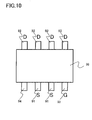
- FIG. 10 is an external view of the semiconductor device of this embodiment. A state in which the power module illustrated in FIG. 9 is stored in one semiconductor package is illustrated.
- the semiconductor package is formed of a sealing unit 99 formed of resin and the like, the source lead wire 91, the drain lead wire 92, the gate lead wire 93, and the lead wire 94 for discharge.
- the normally-off transistor 10, the normally-on transistor 20, and the Zener diode 70 are mounted in the sealing unit 99.
- This embodiment is the semiconductor package in which the lead wire 94 for discharge is adjacent to the source lead wire 91.
- the lead wire 94 for discharge may be connected to the power source 500 as illustrated in FIG. 8 .
- the lead wire 94 for discharge and the adjacent source lead wire 91 may be short-circuited.
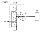
- a semiconductor device of this embodiment is similar to that of the seventh embodiment except that a diode including a second anode connected to a first anode and a second cathode connected to a discharge terminal is further provided between a Zener diode and the discharge terminal.
- a diode including a second anode connected to a first anode and a second cathode connected to a discharge terminal is further provided between a Zener diode and the discharge terminal.
- FIG. 11 is a circuit diagram of the semiconductor device of this embodiment.
- a diode 80 is provided between a discharge terminal 400 and a Zener diode 70.
- devices in a dotted frame in FIG. 11 may be made one semiconductor package.
Landscapes
- Junction Field-Effect Transistors (AREA)
- Semiconductor Integrated Circuits (AREA)
- Electronic Switches (AREA)
Abstract
Description
- This application is based upon and claims the benefit of priority from Japanese Patent Application No.
2013-058840, filed on March 21, 2013 - Embodiments described herein relate generally to a semiconductor device.
- A group-III nitride semiconductor, for example, a GaN (gallium nitride)-based semiconductor is expected as a material of a next-generation power semiconductor device. A GaN-based semiconductor device has a band gap wider than that of a Si (silicon) semiconductor and this may realize higher withstand voltage and lower loss than those of the Si semiconductor device.
- In a GaN-based transistor, a HEMT (high electron mobility transistor) structure using two-dimensional electron gas (2DEG) as a carrier is provided in general. A normal HEMT is a normally-on transistor conducting even when a voltage is not applied to a gate. Therefore, there is a problem that it is difficult to realize a normally-off transistor conducting only when the voltage is applied to the gate.
- In a power source circuit and the like handling a large amount of power of several hundreds to one thousand volts, normally-off operation is required with emphasis on safety. Therefore, a circuit configuration to realize the normally-off operation by cascode connection of a normally-on GaN-based transistor and a normally-off Si transistor is proposed.
- However, in such circuit configuration, there is a problem of a break and deterioration in property of a device when an overvoltage is generated at a connection between the two transistors.
-
-
FIG. 1 is a circuit diagram of a semiconductor device of a first embodiment; -
FIG. 2 is a circuit diagram of a semiconductor device of a second embodiment; -
FIG. 3 is a circuit diagram of a semiconductor device of a third embodiment; -
FIG. 4 is a schematic cross-sectional view of a normally-on transistor of a fourth embodiment; -
FIG. 5 is a view illustrating parasitic capacitances of a GFP and a SFP; -
FIG. 6 is a circuit diagram of a semiconductor device of a fifth embodiment; -
FIG. 7 is a top schematic view of a semiconductor device of a sixth embodiment; -
FIG. 8 is a circuit diagram of a semiconductor device of a seventh embodiment; -
FIG. 9 is a top schematic view of a semiconductor device of an eighth embodiment; -
FIG. 10 is an external view of the semiconductor device of the eighth embodiment; and -
FIG. 11 is a circuit diagram of a semiconductor device of a ninth embodiment. - A semiconductor device of an embodiment is provided with a normally-off transistor including a first source connected to a source terminal, a first drain, and a first gate connected to a gate terminal and a normally-on transistor including a second source connected to the first drain, a second drain connected to a drain terminal, and a second gate connected to the source terminal. A withstand voltage between the first source and the first drain when the normally-off transistor is turned off is lower than a withstand voltage between the second source and the second gate of the normally-on transistor.
- Hereinafter, embodiments of the disclosure are described with reference to the drawings. Meanwhile, in the following description, the same reference numeral is assigned to the same member and the like and the description of the member and the like once described is appropriately omitted.
- In this specification, the semiconductor device is a concept including a power module in which a plurality of devices such as a discrete semiconductor are combined, an intelligent power module in which a driver circuit which drives the devices and a self-protection function are incorporated in a plurality of devices such as the discrete semiconductor, or an entire system provided with the power module and the intelligent power module.
- A semiconductor device of this embodiment is provided with a source terminal, a drain terminal, a gate terminal, a normally-off transistor including a first source connected to the source terminal, a first drain, and a first gate connected to the gate terminal, and a normally-on transistor including a second source connected to the first drain, a second drain connected to the drain terminal, and a second gate connected to the source terminal. A withstand voltage between the first source and the first drain when the normally-off transistor is turned off is lower than a withstand voltage between the second source and the second gate of the normally-on transistor.
-
FIG. 1 is a circuit diagram of the semiconductor device of this embodiment. The semiconductor device of this embodiment is a power module having a rated voltage of 600 V or 1200 V, for example. - In the semiconductor device of this embodiment, a normally-off
transistor 10 and a normally-ontransistor 20 are cascode connected to form the power module. The normally-offtransistor 10 is a Si (silicon)-vertical MOSFET (metal oxide semiconductor field effect transistor), for example. The normally-ontransistor 20 is a GaN (gallium nitride)-based HEMT, for example. The normally-ontransistor 20 is provided with a gate insulation film. - Meanwhile, the normally-off
transistor 10 includes a parasitic body diode not illustrated. - The normally-off
transistor 10 has a device withstand voltage lower than that of the normally-ontransistor 20. The device withstand voltage of the normally-offtransistor 10 is 10 to 30 V, for example. The device withstand voltage of the normally-ontransistor 20 is 600 to 1200 V, for example. - The semiconductor device is provided with a
source terminal 100, adrain terminal 200, and agate terminal 300. The normally-offtransistor 10 includes afirst source 11 connected to thesource terminal 100, afirst drain 12, and afirst gate 13 connected to thegate terminal 300. The normally-ontransistor 20 includes asecond source 21 connected to thefirst drain 12, asecond drain 22 connected to thedrain terminal 200, and asecond gate 23 connected to thesource terminal 100. - The semiconductor device of this embodiment serves as a normally-off transistor provided with the
source terminal 100, thedrain terminal 200, and thegate terminal 300 by the above-described configuration. - In the semiconductor device of this embodiment, the withstand voltage between the
first source 11 and thefirst drain 12 when the normally-offtransistor 10 is turned off is lower than the withstand voltage between thesecond source 21 and thesecond gate 23 of the normally-ontransistor 20. Specifically, an avalanche breakdown voltage of the normally-offtransistor 10 is designed to be lower than a withstand voltage of the gate insulation film of the normally-ontransistor 20. - The avalanche breakdown voltage of the normally-off
transistor 10 is specified by a withstand voltage of the parasitic body diode of the normally-offtransistor 10 or a punch-through withstand voltage of a channel unit. It is possible to adjust the avalanche breakdown voltage of the normally-offtransistor 10 by adjusting impurity concentration and an impurity profile of an impurity layer forming the normally-offtransistor 10, for example. - It is possible to directly estimate the avalanche breakdown voltage of the normally-off
transistor 10 and the withstand voltage of the gate insulation film of the normally-ontransistor 20 by putting a measuring needle on an electrode of the normally-offtransistor 10 and that of the normally-ontransistor 20, for example. - In a circuit configuration in which the normally-off
transistor 10 and the normally-ontransistor 20 are cascode connected, an overvoltage might be generated during device operation at a connection between the normally-offtransistor 10 and the normally-on transistor 20 (hereinafter, also simply referred to as a connection), that is to say, thefirst drain 12 of the normally-offtransistor 10 or thesecond source 21 of the normally-ontransistor 20. The overvoltage might be generated by voltage dividing of a high voltage applied between thesource terminal 100 and thedrain terminal 200 at a parasitic capacitance ratio between the normally-offtransistor 10 and the normally-ontransistor 20 when the semiconductor device shifts from an on-state to an off-state, for example. Alternatively, this might be generated by the voltage dividing of the high voltage applied between thesource terminal 100 and thedrain terminal 200 at a leakage current ratio between the normally-offtransistor 10 and the normally-ontransistor 20 when the semiconductor device is turned off. - When the overvoltage is generated, a high voltage is applied between the
second source 21 and thesecond gate 23 of the normally-ontransistor 20. When the high voltage becomes equal to or higher than the withstand voltage of the gate insulation film, a leakage current of the gate insulation film of the normally-ontransistor 20 might increase or the gate insulation film might be broken. When the leakage current of the gate insulation film of the normally-ontransistor 20 increases or when the gate insulation film is broken, this brings operation failure of the semiconductor device. Therefore, reliability of the semiconductor device is deteriorated. - Even when the gate insulation film has no problem, since the over voltage is applied between the
second source 21 and thesecond gate 23 of the normally-ontransistor 20, a charge is trapped on a side of thesecond source 21. According to this, a current collapse might occur. When the current collapse occurs, an on-state current decreases and the operation failure arises. Therefore, the reliability of the semiconductor device is deteriorated. - In this embodiment, the avalanche breakdown voltage of the normally-off
transistor 10 is designed to be lower than the withstand voltage of the gate insulation film of the normally-ontransistor 20. According to this, the withstand voltage between the first source and the first drain when the normally-off transistor is turned off is made lower than the withstand voltage between the second source and the second gate of the normally-on transistor. - Therefore, even when the overvoltage is generated at the connection, an avalanche breakdown of the normally-
off transistor 10 occurs, so that it is possible to release the charge at the connection. Therefore, it becomes possible to make the voltage applied between thesecond source 21 and thesecond gate 23 of the normally-ontransistor 20 lower than the withstand voltage of the gate insulation film of the normally-ontransistor 20. Therefore, an increase in the leakage current of the gate insulation film of the normally-ontransistor 20 and a break of the gate insulation film are prevented. The current collapse is also prevented. Therefore, the reliability of the semiconductor device is improved. - Meanwhile, the withstand voltage of the gate insulation film of the normally-on
transistor 20 is higher than 30 V in general. Therefore, the avalanche breakdown voltage of the normally-off transistor 10 is desirably not higher than 30 V. - The avalanche breakdown voltage is desirably sufficiently higher than an absolute value of a threshold (Vth) of the normally-on
transistor 20. This is for surely turning off the normally-ontransistor 20. From this point of view, the avalanche breakdown voltage of the normally-off transistor 10 is desirably not lower than an absolute value of the threshold (Vth) of the normally-ontransistor 20 + 5 V. If Vth = -10 V is satisfied, the avalanche breakdown voltage of the normally-off transistor 10 is desirably not lower than 15 V. - A product of an on-resistance and a rated current of the normally-
off transistor 10 is desirably not higher than 2 V. If the product is 2 V or so, it is possible to sufficiently inhibit a decrease in gate bias of the normally-ontransistor 20 by a voltage drop occurring in the normally-off transistor 10. Therefore, current loss due to the decrease in the gate bias may be minimized. - A semiconductor device of this embodiment is different from that of the first embodiment in that a Zener diode including a first anode connected to a first source and a first cathode connected to a first drain and a second source having a Zener voltage lower than an avalanche breakdown voltage of a normally-off transistor is further provided. The description of contents overlapped with those of the first embodiment is not repeated.
-
FIG. 2 is a circuit diagram of the semiconductor device of this embodiment. In the semiconductor device of this embodiment, aZener diode 30 is provided in parallel with a normally-off transistor 10. - The
Zener diode 30 includes afirst anode 31 and afirst cathode 32. Thefirst anode 31 is connected to afirst source 11. Thefirst cathode 32 is connected to afirst drain 12 and asecond source 21. - The Zener voltage of the
Zener diode 30 is set to be lower than the avalanche breakdown voltage of the normally-off transistor 10. The Zener voltage is also set to be lower than a withstand voltage of a gate insulation film of a normally-ontransistor 20. According to this, a withstand voltage between thefirst source 11 and thefirst drain 12 when the normally-off transistor 10 is turned off becomes lower than a withstand voltage between thesecond source 21 and asecond gate 23 of the normally-ontransistor 20. - In the semiconductor device of this embodiment, when an overvoltage is generated at a connection between the normally-
off transistor 10 and the normally-ontransistor 20, a charge is released to theZener diode 30 to pass through thesource terminal 100 when the overvoltage reaches the Zener voltage. Therefore, an increase in voltage at the connection is inhibited and an increase in leakage current of the gate insulation film of the normally-ontransistor 20 and a break of the gate insulation film are prevented. A current collapse is also prevented. Therefore, reliability of the semiconductor device is improved. - The Zener voltage of the
Zener diode 30 may be controlled with higher accuracy as compared to the avalanche breakdown voltage of the normally-off transistor 10. Therefore, in the semiconductor device of this embodiment, it becomes possible to inhibit the overvoltage at the connection in a more stable manner than in the first embodiment by using theZener diode 30. Even when an unexpected high voltage such as noise is applied to thefirst drain 12 of the normally-off transistor 10, the charge may be released by theZener diode 30, so that this also contributes to protect the normally-off transistor 10. - A semiconductor device of this embodiment is different from that of the second embodiment in that a diode including a second anode connected to a first drain and a second source and a second cathode connected to a first cathode provided between the first drain and the second source, and a Zener diode and a capacitor provided between the first cathode and the second cathode, and a first source in parallel with the Zener diode are further provided. The description of contents overlapped with those of the second embodiment is not repeated.
-
FIG. 3 is a circuit diagram of the semiconductor device of this embodiment. In the semiconductor device of this embodiment, adiode 40 is provided on a side of a drain of a normally-off transistor 10. AZener diode 30 is provided in parallel with the normally-off transistor 10. Further, acapacitor 50 is provided in parallel with theZener diode 30. - The
diode 40 is provided between afirst drain 12 and asecond source 21, and theZener diode 30. Thediode 40 includes asecond anode 41 and asecond cathode 42. The second anode is connected to thefirst drain 12 and thesecond source 21. Thesecond cathode 42 is connected to afirst cathode 32. - The
capacitor 50 is provided between thefirst cathode 32 and thesecond cathode 42, and afirst source 11 in parallel with theZener diode 30. - The
diode 40 prevents backflow of a charge from a side of thecapacitor 50. Thediode 40 is a PiN diode or a Schottky barrier diode, for example. - According to this embodiment, when an overvoltage is generated at a connection between the normally-
off transistor 10 and a normally-ontransistor 20, the charge is temporarily accumulated in thecapacitor 50. Then, the accumulated charge is released to a side of asource terminal 100 by theZener diode 30. According to this, an increase in voltage at the connection is inhibited and an increase in leakage current of a gate insulation film of the normally-ontransistor 20 and a break of the gate insulation film are prevented. A current collapse is also prevented. Therefore, reliability of the semiconductor device is improved. - In this embodiment, since the charge is temporarily accumulated in the
capacitor 50, theZener diode 30 may be an inexpensive diode having a small parasitic capacitance. Therefore, an inexpensive semiconductor device may be realized. - A capacitance of the
capacitor 50 is connected in series to a capacitance of thediode 40 between thefirst source 11 and thefirst drain 12 of the normally-off transistor 10. A type having a parasitic capacitance significantly smaller than that of theZener diode 30 may be selected as thediode 40 for a current required for absorbing the charge. Therefore, the capacitance of thecapacitor 50 contributes little as a parasitic capacitance of the normally-off transistor 10 by making the capacitance of thediode 40 sufficiently smaller than the capacitance of thecapacitor 50. Therefore, a decrease in operation speed of the normally-off transistor 10 and an increase in loss due to an increase in the parasitic capacitance may be inhibited. - In a semiconductor device of this embodiment, a normally-on transistor includes a gate field plate (hereinafter, also referred to as GFP). Other configuration is similar to that of the first embodiment. Therefore, the description of contents overlapped with those of the first embodiment is not repeated.
-
FIG. 4 is a schematic cross-sectional view of the normally-on transistor of this embodiment. The normally-on transistor is a GaN (gallium nitride)-based HEMT provided with a gate insulation film. - A normally-on transistor 20 (
FIG. 1 ) is formed on anitride semiconductor layer 161 on asubstrate 160. Thesubstrate 160 is formed of silicon (Si), for example. - A buffer layer (not illustrated) is provided between the
substrate 160 and thenitride semiconductor layer 161. The buffer layer serves to reduce lattice mismatch between thesubstrate 160 and thenitride semiconductor layer 161. The buffer layer is formed of a multilayer structure of aluminum gallium nitride (AlxGa1-xN (0 < x < 1)), for example. - The
nitride semiconductor layer 161 is provided with a laminated structure of an operation layer (channel layer) 161 a and a barrier layer (electron supply layer) 161 b. Theoperation layer 161 a is formed of gallium nitride (GaN), for example, and thebarrier layer 161b is formed of aluminum gallium nitride (AlGaN), for example. - A heterojunction interface is formed between the
operation layer 161 a and thebarrier layer 161b. - A
gate electrode 164 is formed on thenitride semiconductor layer 161 with a firstsilicon nitride film 162 interposed therebetween. The firstsilicon nitride film 162 serves as a gate insulation film. Thegate electrode 164 is, for example, a metal electrode. The metal electrode is, for example, a nickel (Ni) electrode, a titanium (Ti) electrode, or an aluminum (Al) electrode. - A
source electrode 166 and adrain electrode 168 are provided on thenitride semiconductor layer 161 with thegate electrode 164 interposed therebetween. Each of thesource electrode 166 and thedrain electrode 168 is separated from thegate electrode 164. - A second
silicon nitride film 170 is formed between thesource electrode 166 and thegate electrode 164 and between thedrain electrode 168 and thegate electrode 164 on thenitride semiconductor layer 161. The secondsilicon nitride film 170 is formed so as to be in contact with a surface of thenitride semiconductor layer 161. The secondsilicon nitride film 170 serves as a surface protection film (or a passivation film) which protects the surface of thenitride semiconductor layer 161 between thegate electrode 164 and thesource electrode 166 and between thegate electrode 164 and thedrain electrode 168. - The
gate electrode 164 extends to a side of thedrain electrode 168 on the secondsilicon nitride film 170. A part extended to thedrain electrode 168 side of thegate electrode 164 serves as so-called the gate field plate. Meanwhile, a length (d in the drawing) of the part extended to thedrain electrode 168 side of thegate electrode 164, that is to say, the part extended to thedrain electrode 168 side from a lower end on thedrain electrode 168 side of thegate electrode 164 is not shorter than 1 µm. - The gate field plate serves to reduce an electric field in a drain region between the
gate electrode 164 and thedrain electrode 168 to inhibit a current collapse. There is a source field plate (hereinafter, also referred to as SFP) obtained by extending thesource electrode 166 to thedrain electrode 168 side as a structure to provide a similar function. -
FIG. 5 is a view illustrating parasitic capacitances of the GFP and the SFP. A source-drain capacitance (Cds), a source-gate capacitance (Cgs), and a drain-gate capacitance (Cgd) of the GFP and those of the SFP are compared. A capacitance simulation result is illustrated. In the drawing, a solid line indicates the GFP and a dotted line indicates the SFP. - As is clear from
FIG. 5 , in the GFP, although the drain-gate capacitance (Cgd) is larger than that in the SFP, the source-drain capacitance (Cds) and the source-gate capacitance (Cgs) are smaller than those in the SFP. - In general, the parasitic capacitance of the transistor is desirably small from a viewpoint of avoiding a decrease in operation speed and an increase in loss. Especially, the drain-gate capacitance (Cgd) has a large effect on parasitic oscillation and a switching speed, so that this is desirably small.
- In the semiconductor device of this embodiment, a
second gate 23 of the normally-ontransistor 20 is connected to afirst source 11 of a normally-off transistor 10 as illustrated in the circuit diagram inFIG. 1 . Transistor operation is performed by raising a voltage of asecond source 21 of the normally-ontransistor 20, so that charge/discharge of thesecond gate 23 is not directly performed during the operation. Therefore, it is possible to eliminate the effect of the drain-gate capacitance (Cgd) on the operation. - Therefore, in the semiconductor device of this embodiment, that is to say, in a configuration in which the normally-
off transistor 10 and the normally-ontransistor 20 are cascode connected, the GFP having small source-drain capacitance (Cds) and source-gate capacitance (Cgs) is desirable as a structure to realize a reduction in collapse as compared to the SFP. - According to this embodiment, in addition to an effect of improving reliability similar to that of the first embodiment, it becomes possible to inhibit the current collapse by inhibiting the effect of the parasitic capacitance on a device property by the GFP. Therefore, the semiconductor device with further improved reliability is realized.
- Meanwhile, as for the GFP, although the structure in which the gate electrode itself extends to the drain side is described as an example, a configuration in which a GFP electrode having same potential as the gate electrode is provided on an upper layer and the like of the gate electrode separately from the gate electrode is also possible.
- A semiconductor device of this embodiment is different from the semiconductor device of the second embodiment in that a Schottky barrier diode including a third anode connected to a first source and a third cathode connected to a first drain and a second source having a forward drop voltage lower than a forward drop voltage of a parasitic body diode of a normally-off transistor provided between the first drain and the second source, and the first source in parallel with a Zener diode is further provided. Hereinafter, the description of contents overlapped with those of the first and second embodiments is not repeated.
-
FIG. 6 is a circuit diagram of the semiconductor device of this embodiment. In the semiconductor device of this embodiment, aZener diode 30 is provided in parallel with a normally-off transistor 10. Further, aSchottky barrier diode 60 is provided in parallel with theZener diode 30. - The
Schottky barrier diode 60 is provided with athird anode 61 and athird cathode 62. Thethird anode 61 is connected to afirst source 11. Thethird cathode 62 is connected to afirst drain 12 and asecond source 21. - A forward drop voltage (Vf) of the
Schottky barrier diode 60 is lower than a forward drop voltage (Vf) of the parasitic body diode (not illustrated) of the normally-off transistor. TheSchottky barrier diode 60 is provided between thefirst drain 12 and thesecond source 21, and thefirst source 11 in parallel with theZener diode 30. - When the
Schottky barrier diode 60 is not provided, a current flows through the parasitic body diode of the normally-off transistor 10 in a reflux mode in which asource terminal 100 has a positive voltage relative to adrain terminal 200. In this embodiment, theSchottky barrier diode 60 having the forward drop voltage (Vf) lower than the forward drop voltage (Vf) of the parasitic body diode of the normally-off transistor 10 is provided. According to this, the current flows through theSchottky barrier diode 60 in the reflux mode. - Different from a PiN diode, the Schottky barrier diode operates by using only a majority carrier. Therefore, this is excellent in recovery property as compared to the PiN diode. Therefore, in addition to the effects of the first and second embodiments, it becomes possible to improve the recovery property in the reflux mode in this embodiment. Therefore, the semiconductor device excellent in reliability and recovery property may be realized. A normally-on
transistor 20 bears a large part of a withstand voltage, so that a low withstand voltage type may be selected as theSchottky barrier diode 60. According to this, it is possible to realize high withstand voltage body diode operation with a Vf property and the recovery property similar to those of the low withstand voltage type. - Since the forward drop voltage (Vf) is small, it is also possible to reduce conduction loss and switching loss in the reflux mode. Application of an overvoltage at a connection is inhibited by a parasitic capacitance of the
Schottky barrier diode 60. Since it is possible to release a charge from the connection by a leakage current of theSchottky barrier diode 60, the application of the overvoltage at the connection is inhibited. Therefore, the semiconductor device with further improved reliability is realized. - Meanwhile, since the Schottky barrier diode is not an avalanche-proof Schottky barrier diode, the withstand voltage of the
Schottky barrier diode 60 is desirably higher than an avalanche breakdown voltage of the normally-off transistor 10. - A semiconductor device of this embodiment is further provided with a substrate, a source lead wire, a drain lead wire, and a gate lead wire. A normally-off transistor, a normally-on transistor, a Zener diode, and a Schottky barrier diode are mounted on the substrate. The Schottky barrier diode, the Zener diode, and the normally-on transistor are arranged in this order from a side of the source lead wire to a side of the drain lead wire. The normally-off transistor and the normally-on transistor are arranged in this order from the side of the source lead wire to the side of the drain lead wire. The source lead wire is connected to a third anode and a first source and the drain lead wire is connected to a second drain.
- This embodiment is obtained by embodying the circuit configuration of the fifth embodiment as a power module. Hereinafter, the description of contents overlapped with those of the fifth embodiment is not repeated.
-
FIG. 7 is a top schematic view of the semiconductor device of this embodiment. - The semiconductor device of this embodiment is provided with a
substrate 90, asource lead wire 91, adrain lead wire 92, and agate lead wire 93. Thesource lead wire 91, thedrain lead wire 92, and thegate lead wire 93 correspond to asource terminal 100, adrain terminal 200, and agate terminal 300, respectively. - A metal
conductive material 95, for example, is present on at least a surface of thesubstrate 90. A normally-off transistor 10, a normally-ontransistor 20, aZener diode 30, and aSchottky barrier diode 60 are mounted on thesubstrate 90. Each of the normally-off transistor 10, the normally-ontransistor 20, theZener diode 30, and theSchottky barrier diode 60 is a semiconductor chip, for example, and is mounted on theconductive material 95 of the substrate with conductive paste and soldering, for example. - The
Schottky barrier diode 60, theZener diode 30, and the normally-ontransistor 20 are arranged in this order from a side of thesource lead wire 91 to a side of thedrain lead wire 92. The normally-off transistor 10 and the normally-ontransistor 20 are arranged in this order from the side of thesource lead wire 91 to the side of thedrain lead wire 92 on thesubstrate 90. - The
source lead wire 91 is connected to athird anode 61 and afirst source 11 and thedrain lead wire 92 is connected to asecond drain 22. Each connection is performed by wire bonding, for example. A material such as copper (Cu) and aluminum (Al) is used, for example, in the wire bonding. - According to this embodiment, the normally-
off transistor 10 and the normally-ontransistor 20 are arranged in this order from the side of thesource lead wire 91 to the side of thedrain lead wire 92. According to this, a pathway through which an on-state current flows of the semiconductor device may be shortened. This arrangement eliminates parasitic inductance of the pathway of the on-state current as far as possible to decrease conduction loss. - By arranging the
Schottky barrier diode 60 and the normally-ontransistor 20 in this order from the side of thesource lead wire 91 to the side of thedrain lead wire 92, it becomes possible to shorten the pathway of the current flowing through the pathway from thesource lead wire 91 through theSchottky barrier diode 60 and the normally-ontransistor 20 to thedrain lead wire 92 in a reflux mode. Therefore, it becomes possible to decrease the conduction loss in the reflux mode. - In the Schottky barrier diode, a leakage current has large temperature dependency. The normally-on
transistor 20 being a GaN-based HEMT emits heat the most in the semiconductor device of this embodiment. Therefore, it is possible to increase a distance between theSchottky barrier diode 60 and the normally-ontransistor 20 by arranging theZener diode 30 between theSchottky barrier diode 60 and the normally-ontransistor 20. Therefore, property fluctuation of theSchottky barrier diode 60 may be inhibited. - The
Zener diode 30 which inhibits an overvoltage at a connection is provided so as to be adjacent to the normally-off transistor 10 and thefirst source 11 and thefirst anode 31 are directly bonded. According to this, a pathway to release a charge from the connection becomes shorter and application of the overvoltage may be efficiently inhibited. - As described above, according to this embodiment, in addition to the effect of the fifth embodiment, it is possible to realize the semiconductor device excellent in property by appropriately arranging and connecting each device.
- A semiconductor device of this embodiment is provided with a source terminal, a drain terminal, a gate terminal, a discharge terminal, a normally-off transistor including a first source connected to the source terminal, a first drain, and a first gate connected to the gate terminal, a normally-on transistor including a second source connected to the first drain, a second drain connected to the drain terminal, and a second gate connected to the source terminal, and a Zener diode including a first anode connected to the discharge terminal and a first cathode connected to the first drain and the second source having a Zener voltage lower than a withstand voltage between the second source and the second gate of the normally-on transistor and lower than an avalanche breakdown voltage of the normally-off transistor.
-
FIG. 8 is a circuit diagram of the semiconductor device of this embodiment. This is similar to that of the first embodiment in that a normally-off transistor 10 and a normally-ontransistor 20 are cascode connected to form a power module. Hereinafter, the description of contents overlapped with those of the first embodiment is not repeated. - The semiconductor device of this embodiment is provided with a
source terminal 100, adrain terminal 200, agate terminal 300, and adischarge terminal 400. The normally-off transistor 10 includes afirst source 11 connected to thesource terminal 100, afirst drain 12, and afirst gate 13 connected to thegate terminal 300. The normally-ontransistor 20 includes asecond source 21 connected to thefirst drain 12, asecond drain 22 connected to thedrain terminal 200, and asecond gate 23 connected to thesource terminal 100. - A
Zener diode 70 having the Zener voltage lower than the withstand voltage between the second source and the second gate of the normally-ontransistor 20 is provided. The Zener voltage is also lower than the avalanche breakdown voltage of the normally-off transistor 10. - The
Zener diode 70 includes afirst anode 71 and a first cathode 72. Thefirst anode 71 is connected to thedischarge terminal 400. The first cathode 72 is connected to thefirst drain 12 and thesecond source 21. - A
power source 500 is connected to thedischarge terminal 400 through adiode 80. Thesecond diode 80 includes asecond anode 81 and asecond cathode 82. Thesecond diode 80 is a PiN diode, for example. Thepower source 500 is a power source of a control circuit which controls the cascode connected normally-off transistor 10 and normally-ontransistor 20, for example. - The
second anode 81 of thesecond diode 80 is connected to thedischarge terminal 400. Thesecond cathode 82 is connected to thepower source 500. Thediode 80 inhibits a current from flowing from a side of thepower source 500 to a connection. - According to this embodiment, when an overvoltage is generated at the connection between the normally-
off transistor 10 and the normally-ontransistor 20, a charge is released to theZener diode 70 to pass through thedischarge terminal 400 when the overvoltage reaches the Zener voltage. Therefore, an increase in voltage at the connection is inhibited and an increase in leakage current of a gate insulation film of the normally-ontransistor 20 and a break of the gate insulation film are prevented. A current collapse is also prevented. Therefore, reliability of the semiconductor device is improved. Since the charge generated at the connection by the overvoltage is put into thepower source 500 for regeneration, energy saving of an entire system of the semiconductor device is realized. - Meanwhile, the Zener voltage is desirably optimized by a voltage of the
power source 500 and a voltage value allowed at the connection. For example, when the voltage of thepower source 500 is 5 V and the voltage allowed at the connection is 20 V, the Zener voltage may be adjusted to approximately 15 V. - A semiconductor device of this embodiment is provided with a substrate, a source lead wire, a drain lead wire, a gate lead wire, and a lead wire for discharge adjacent to the gate lead wire. A normally-off transistor, a normally-on transistor, and a Zener diode are mounted on the substrate. A first source is connected to the source lead wire, a second drain is connected to the drain lead wire, a first gate is connected to the gate lead wire, and a first anode is connected to the lead wire for discharge.
- This embodiment is obtained by embodying the circuit configuration of the seventh embodiment as a power module on which a device is mounted. Hereinafter, the description of contents overlapped with those of the seventh embodiment is not repeated.
-
FIG. 9 is a top schematic view of the semiconductor device of this embodiment.FIG. 9 illustrates a state in which devices in a dotted frame inFIG. 8 is mounted. - A
source lead wire 91, adrain lead wire 92, agate lead wire 93, alead wire 94 for discharge adjacent to thesource lead wire 91, and asubstrate 90 are provided. A normally-off transistor 10, a normally-ontransistor 20, and aZener diode 70 are mounted on thesubstrate 90, afirst source 11 is connected to thesource lead wire 91, asecond drain 22 is connected to thedrain lead wire 92, afirst gate 13 is connected to thegate lead wire 93, and afirst anode 71 is connected to thelead wire 94 for discharge. -
FIG. 10 is an external view of the semiconductor device of this embodiment. A state in which the power module illustrated inFIG. 9 is stored in one semiconductor package is illustrated. - The semiconductor package is formed of a sealing
unit 99 formed of resin and the like, thesource lead wire 91, thedrain lead wire 92, thegate lead wire 93, and thelead wire 94 for discharge. The normally-off transistor 10, the normally-ontransistor 20, and theZener diode 70 are mounted in the sealingunit 99. - This embodiment is the semiconductor package in which the
lead wire 94 for discharge is adjacent to thesource lead wire 91. In the semiconductor package of this embodiment, when a charge generated by an overvoltage at a connection between the normally-off transistor 10 and the normally-ontransistor 20 is wanted to be regenerated, thelead wire 94 for discharge may be connected to thepower source 500 as illustrated inFIG. 8 . On the other hand, when it is wanted to release the charge generated by the overvoltage at the connection to a side of thesource terminal 100 as illustrated in the second embodiment, thelead wire 94 for discharge and the adjacentsource lead wire 91 may be short-circuited. - According to this embodiment, it is possible to provide the semiconductor package capable of easily realizing an appropriate circuit configuration depending on intended usage.
- A semiconductor device of this embodiment is similar to that of the seventh embodiment except that a diode including a second anode connected to a first anode and a second cathode connected to a discharge terminal is further provided between a Zener diode and the discharge terminal. Hereinafter, the description of contents overlapped with those of the seventh embodiment is not repeated.
-
FIG. 11 is a circuit diagram of the semiconductor device of this embodiment. - Different from the seventh embodiment, in the semiconductor device of this embodiment, a
diode 80 is provided between adischarge terminal 400 and aZener diode 70. For example, devices in a dotted frame inFIG. 11 may be made one semiconductor package. - It is possible to obtain an effect similar to that of the seventh embodiment also by this embodiment. Additionally, by mounting the
diode 80 for preventing backflow in the semiconductor package, it becomes possible to realize a more compact system. - While certain embodiments have been described, these embodiments have been presented by way of example only, and are not intended to limit the scope of the inventions. Indeed, the semiconductor device described herein may be embodied in a variety of other forms; furthermore, various omissions, substitutions and changes in the form of the devices and methods described herein may be made without departing from the spirit of the inventions. The accompanying claims and their equivalents are intended to cover such forms or modifications as would fall within the scope and spirit of the inventions.
Claims (12)
- A semiconductor device, comprising:a normally-off transistor having a first source connected to a source terminal, a first drain, and a first gate connected to a gate terminal; anda normally-on transistor having a second source connected to the first drain, a second drain connected to a drain terminal, and a second gate connected to the source terminal, whereina withstand voltage between the first source and the first drain when the normally-off transistor is turned off is lower than the withstand voltage between the second source and the second gate of the normally-on transistor.
- The device according to claim 1, wherein the normally-on transistor is a GaN-based HEMT.
- The device according to claim 1, further comprising a Zener diode having a first anode connected to the first source and a first cathode connected to the first drain and the second source, the Zener diode having a Zener voltage lower than an avalanche breakdown voltage of the normally-off transistor.
- The device according to claim 3, further comprising
a diode provided between the first drain and the Zener diode, the diode having a second anode connected to the first drain and a second cathode connected to the first cathode, and
a capacitor provided between the first cathode and the second cathode, and the first source in parallel with the Zener diode. - The device according to claim 2, wherein the normally-on transistor has a gate field plate.
- The device according to claim 3, further comprising a Schottky barrier diode having a third anode connected to the first source and a third cathode connected to the first drain, the Schottky barrier diode having a forward drop voltage lower than a forward drop voltage of a parasitic body diode of the normally-off transistor, the parasitic body diode provided between the first drain and the first source in parallel with the Zener diode.
- The device according to claim 6, further comprising
a substrate, a source lead wire, a drain lead wire, and a gate lead wire, wherein
the Schottky barrier diode, the Zener diode, and the normally-on transistor are arranged in this order on the substrate from a side of the source lead wire to a side of the drain lead wire,
the normally-off transistor and the normally-on transistor are arranged in this order from the side of the source lead wire to the side of the drain lead wire,
the source lead wire is connected to the third anode and the first source, and
the drain lead wire is connected to the second drain. - The device according to claim 1, wherein the normally-off transistor is a Si-vertical MOSFET.
- A semiconductor device, comprising:a normally-off transistor having a first source connected to a source terminal, a first drain, and a first gate connected to a gate terminal;a normally-on transistor having a second source connected to the first drain, a second drain connected to a drain terminal, and a second gate connected to the source terminal,and a Zener diode having a first anode connected to a discharge terminal and a first cathode connected to the first drain, the Zener diode having a Zener voltage lower than a withstand voltage between the second source and the second gate of the normally-on transistor and lower than an avalanche breakdown voltage of the normally-off transistor.
- The device according to claim 9, further comprising a diode having a second anode connected to the first anode and a second cathode connected to the discharge terminal between the Zener diode and the discharge terminal.
- The device according to claim 9, wherein the discharge terminal is connected to a power source.
- The device according to claim 9, further comprising
a substrate, a source lead wire, a drain lead wire, a gate lead wire, and a lead wire for discharge adjacent to the gate lead wire,
wherein the normally-off transistor, the normally-on transistor, and the Zener diode are mounted on the substrate,
the first source is connected to the source lead wire,
the second drain is connected to the drain lead wire,
the first gate is connected to the gate lead wire, and
the first anode is connected to the lead wire for discharge.
Applications Claiming Priority (1)
| Application Number | Priority Date | Filing Date | Title |
|---|---|---|---|
| JP2013058840A JP6113542B2 (en) | 2013-03-21 | 2013-03-21 | Semiconductor device |
Publications (3)
| Publication Number | Publication Date |
|---|---|
| EP2811518A2 true EP2811518A2 (en) | 2014-12-10 |
| EP2811518A3 EP2811518A3 (en) | 2015-03-25 |
| EP2811518B1 EP2811518B1 (en) | 2018-03-28 |
Family
ID=50112824
Family Applications (1)
| Application Number | Title | Priority Date | Filing Date |
|---|---|---|---|
| EP14155485.7A Active EP2811518B1 (en) | 2013-03-21 | 2014-02-17 | Semiconductor device |
Country Status (3)
| Country | Link |
|---|---|
| US (1) | US9123536B2 (en) |
| EP (1) | EP2811518B1 (en) |
| JP (1) | JP6113542B2 (en) |
Cited By (1)
| Publication number | Priority date | Publication date | Assignee | Title |
|---|---|---|---|---|
| CN106571799A (en) * | 2015-08-27 | 2017-04-19 | 耐智亚有限公司 | Semiconductor device and associated method |
Families Citing this family (14)
| Publication number | Priority date | Publication date | Assignee | Title |
|---|---|---|---|---|
| JP2016139996A (en) | 2015-01-28 | 2016-08-04 | 株式会社東芝 | Semiconductor device |
| JP2016139997A (en) * | 2015-01-28 | 2016-08-04 | 株式会社東芝 | Semiconductor device |
| US10050620B2 (en) | 2015-02-27 | 2018-08-14 | Renesas Electronics America Inc. | Cascode connected SiC-JFET with SiC-SBD and enhancement device |
| US10756084B2 (en) * | 2015-03-26 | 2020-08-25 | Wen-Jang Jiang | Group-III nitride semiconductor device and method for fabricating the same |
| JP6604125B2 (en) * | 2015-10-02 | 2019-11-13 | サンケン電気株式会社 | Cascode normally-off circuit |
| JP6685870B2 (en) * | 2016-09-15 | 2020-04-22 | 株式会社東芝 | Semiconductor device |
| JP6991776B2 (en) * | 2017-08-02 | 2022-01-13 | ローム株式会社 | Semiconductor device |
| JP6953234B2 (en) | 2017-08-28 | 2021-10-27 | ラピスセミコンダクタ株式会社 | Semiconductor devices and methods for manufacturing semiconductor devices |
| US10840798B1 (en) | 2018-09-28 | 2020-11-17 | Dialog Semiconductor (Uk) Limited | Bidirectional signaling method for high-voltage floating circuits |
| TWI696339B (en) * | 2019-05-21 | 2020-06-11 | 莊陳英 | Switching power converter circuit and cascoded transistor circuit thereof |
| FR3097682B1 (en) * | 2019-06-19 | 2023-01-13 | St Microelectronics Gmbh | Monolithic component comprising a gallium nitride power transistor |
| JP7455604B2 (en) * | 2020-02-14 | 2024-03-26 | 株式会社東芝 | Normally-on transistor drive circuit and drive method |
| JP7374486B2 (en) * | 2020-05-27 | 2023-11-07 | 株式会社パウデック | semiconductor circuit |
| JP2024046114A (en) | 2022-09-22 | 2024-04-03 | 株式会社東芝 | semiconductor equipment |
Family Cites Families (26)
| Publication number | Priority date | Publication date | Assignee | Title |
|---|---|---|---|---|
| FR2678772B1 (en) * | 1991-07-03 | 1997-05-30 | Dassault Electronique | REGULATED SUPPLY DEVICE WITH ACTIVE CIRCUIT, PARTICULARLY FOR TUBES WITH PROGRESSIVE WAVES. |
| JP2002175894A (en) * | 2000-12-08 | 2002-06-21 | Toshiba Lighting & Technology Corp | Power supply unit, discharge lamp lighting device and lighting equipment |
| DE10157250C1 (en) * | 2001-11-22 | 2002-12-05 | Siemens Ag | Semiconducting switch module has circuit for protection against overvoltages arranged in housing and on substrate and electrically connected and thermally coupled to semiconducting body |
| US7202528B2 (en) * | 2004-12-01 | 2007-04-10 | Semisouth Laboratories, Inc. | Normally-off integrated JFET power switches in wide bandgap semiconductors and methods of making |
| US7928702B2 (en) * | 2005-04-13 | 2011-04-19 | International Rectifier Corporation | Driving circuit for use with high voltage depletion-mode semiconductor switches |
| JP4844007B2 (en) * | 2005-05-18 | 2011-12-21 | 富士電機株式会社 | Composite type semiconductor device |
| US7965126B2 (en) * | 2008-02-12 | 2011-06-21 | Transphorm Inc. | Bridge circuits and their components |
| US8084783B2 (en) * | 2008-11-10 | 2011-12-27 | International Rectifier Corporation | GaN-based device cascoded with an integrated FET/Schottky diode device |
| US8816497B2 (en) * | 2010-01-08 | 2014-08-26 | Transphorm Inc. | Electronic devices and components for high efficiency power circuits |
| US8530904B2 (en) * | 2010-03-19 | 2013-09-10 | Infineon Technologies Austria Ag | Semiconductor device including a normally-on transistor and a normally-off transistor |
| US8896131B2 (en) * | 2011-02-03 | 2014-11-25 | Alpha And Omega Semiconductor Incorporated | Cascode scheme for improved device switching behavior |
| WO2012111393A1 (en) * | 2011-02-15 | 2012-08-23 | シャープ株式会社 | Semiconductor device |
| US9859882B2 (en) * | 2011-03-21 | 2018-01-02 | Infineon Technologies Americas Corp. | High voltage composite semiconductor device with protection for a low voltage device |
| US8766375B2 (en) * | 2011-03-21 | 2014-07-01 | International Rectifier Corporation | Composite semiconductor device with active oscillation prevention |
| US8987833B2 (en) * | 2011-04-11 | 2015-03-24 | International Rectifier Corporation | Stacked composite device including a group III-V transistor and a group IV lateral transistor |
| US9343440B2 (en) * | 2011-04-11 | 2016-05-17 | Infineon Technologies Americas Corp. | Stacked composite device including a group III-V transistor and a group IV vertical transistor |
| US20120262220A1 (en) * | 2011-04-13 | 2012-10-18 | Semisouth Laboratories, Inc. | Cascode switches including normally-off and normally-on devices and circuits comprising the switches |
| JP5270713B2 (en) * | 2011-04-19 | 2013-08-21 | シャープ株式会社 | Switching power supply |
| US8598937B2 (en) * | 2011-10-07 | 2013-12-03 | Transphorm Inc. | High power semiconductor electronic components with increased reliability |
| US20140029152A1 (en) * | 2012-03-30 | 2014-01-30 | Semisouth Laboratories, Inc. | Solid-state circuit breakers |
| US20130264654A1 (en) * | 2012-04-06 | 2013-10-10 | Infineon Technologies Dresden Gmbh | Integrated Switching Device with Parallel Rectifier Element |
| JP5996465B2 (en) * | 2013-03-21 | 2016-09-21 | 株式会社東芝 | Semiconductor device |
| JP6201422B2 (en) * | 2013-05-22 | 2017-09-27 | 富士電機株式会社 | Semiconductor device |
| JP6211829B2 (en) * | 2013-06-25 | 2017-10-11 | 株式会社東芝 | Semiconductor device |
| JP6223729B2 (en) * | 2013-06-25 | 2017-11-01 | 株式会社東芝 | Semiconductor device |
| US8958189B1 (en) * | 2013-08-09 | 2015-02-17 | Infineon Technologies Austria Ag | High-voltage semiconductor switch and method for switching high voltages |
-
2013
- 2013-03-21 JP JP2013058840A patent/JP6113542B2/en active Active
-
2014
- 2014-02-17 EP EP14155485.7A patent/EP2811518B1/en active Active
- 2014-02-19 US US14/183,698 patent/US9123536B2/en active Active
Non-Patent Citations (1)
| Title |
|---|
| None |
Cited By (1)
| Publication number | Priority date | Publication date | Assignee | Title |
|---|---|---|---|---|
| CN106571799A (en) * | 2015-08-27 | 2017-04-19 | 耐智亚有限公司 | Semiconductor device and associated method |
Also Published As
| Publication number | Publication date |
|---|---|
| EP2811518B1 (en) | 2018-03-28 |
| JP2014187059A (en) | 2014-10-02 |
| US9123536B2 (en) | 2015-09-01 |
| US20140284655A1 (en) | 2014-09-25 |
| EP2811518A3 (en) | 2015-03-25 |
| JP6113542B2 (en) | 2017-04-12 |
Similar Documents
| Publication | Publication Date | Title |
|---|---|---|
| US9123536B2 (en) | Semiconductor device | |
| JP6223729B2 (en) | Semiconductor device | |
| US9653449B2 (en) | Cascoded semiconductor device | |
| JP6211829B2 (en) | Semiconductor device | |
| US9679880B2 (en) | Cascode power transistors | |
| US10084442B2 (en) | Semiconductor device | |
| US9431391B2 (en) | Gallium nitride hemt device with a mosfet in series coupled to diodes for protection of high-voltage | |
| US8860090B2 (en) | Nitride semiconductor device | |
| CN111415916A (en) | Semiconductor device and semiconductor package | |
| EP2511953A1 (en) | Stacked composite device including a group III-V transistor and a group IV lateral transistor | |
| US20160248422A1 (en) | Switching circuit, semiconductor switching arrangement and method | |
| TWI584562B (en) | Semiconductor device |
Legal Events
| Date | Code | Title | Description |
|---|---|---|---|
| PUAI | Public reference made under article 153(3) epc to a published international application that has entered the european phase |
Free format text: ORIGINAL CODE: 0009012 |
|
| 17P | Request for examination filed |
Effective date: 20140217 |
|
| AK | Designated contracting states |
Kind code of ref document: A2 Designated state(s): AL AT BE BG CH CY CZ DE DK EE ES FI FR GB GR HR HU IE IS IT LI LT LU LV MC MK MT NL NO PL PT RO RS SE SI SK SM TR |
|
| AX | Request for extension of the european patent |
Extension state: BA ME |
|
| PUAL | Search report despatched |
Free format text: ORIGINAL CODE: 0009013 |
|
| AK | Designated contracting states |
Kind code of ref document: A3 Designated state(s): AL AT BE BG CH CY CZ DE DK EE ES FI FR GB GR HR HU IE IS IT LI LT LU LV MC MK MT NL NO PL PT RO RS SE SI SK SM TR |
|
| AX | Request for extension of the european patent |
Extension state: BA ME |
|
| RIC1 | Information provided on ipc code assigned before grant |
Ipc: H03K 17/567 20060101ALI20150217BHEP Ipc: H01L 27/06 20060101ALN20150217BHEP Ipc: H01L 25/18 20060101AFI20150217BHEP Ipc: H01L 27/085 20060101ALN20150217BHEP |
|
| GRAP | Despatch of communication of intention to grant a patent |
Free format text: ORIGINAL CODE: EPIDOSNIGR1 |
|
| STAA | Information on the status of an ep patent application or granted ep patent |
Free format text: STATUS: GRANT OF PATENT IS INTENDED |
|
| RIC1 | Information provided on ipc code assigned before grant |
Ipc: H01L 27/06 20060101ALN20170913BHEP Ipc: H01L 25/18 20060101AFI20170913BHEP Ipc: H01L 27/085 20060101ALN20170913BHEP Ipc: H01L 27/02 20060101ALI20170913BHEP Ipc: H03K 17/567 20060101ALI20170913BHEP |
|
| INTG | Intention to grant announced |
Effective date: 20171018 |
|
| GRAS | Grant fee paid |
Free format text: ORIGINAL CODE: EPIDOSNIGR3 |
|
| GRAA | (expected) grant |
Free format text: ORIGINAL CODE: 0009210 |
|
| STAA | Information on the status of an ep patent application or granted ep patent |
Free format text: STATUS: THE PATENT HAS BEEN GRANTED |
|
| AK | Designated contracting states |
Kind code of ref document: B1 Designated state(s): AL AT BE BG CH CY CZ DE DK EE ES FI FR GB GR HR HU IE IS IT LI LT LU LV MC MK MT NL NO PL PT RO RS SE SI SK SM TR |
|
| REG | Reference to a national code |
Ref country code: GB Ref legal event code: FG4D |
|
| REG | Reference to a national code |
Ref country code: CH Ref legal event code: EP |
|
| REG | Reference to a national code |
Ref country code: AT Ref legal event code: REF Ref document number: 984130 Country of ref document: AT Kind code of ref document: T Effective date: 20180415 |
|
| REG | Reference to a national code |
Ref country code: IE Ref legal event code: FG4D |
|
| REG | Reference to a national code |
Ref country code: DE Ref legal event code: R096 Ref document number: 602014022880 Country of ref document: DE |
|
| PG25 | Lapsed in a contracting state [announced via postgrant information from national office to epo] |
Ref country code: HR Free format text: LAPSE BECAUSE OF FAILURE TO SUBMIT A TRANSLATION OF THE DESCRIPTION OR TO PAY THE FEE WITHIN THE PRESCRIBED TIME-LIMIT Effective date: 20180328 Ref country code: NO Free format text: LAPSE BECAUSE OF FAILURE TO SUBMIT A TRANSLATION OF THE DESCRIPTION OR TO PAY THE FEE WITHIN THE PRESCRIBED TIME-LIMIT Effective date: 20180628 Ref country code: FI Free format text: LAPSE BECAUSE OF FAILURE TO SUBMIT A TRANSLATION OF THE DESCRIPTION OR TO PAY THE FEE WITHIN THE PRESCRIBED TIME-LIMIT Effective date: 20180328 Ref country code: LT Free format text: LAPSE BECAUSE OF FAILURE TO SUBMIT A TRANSLATION OF THE DESCRIPTION OR TO PAY THE FEE WITHIN THE PRESCRIBED TIME-LIMIT Effective date: 20180328 |
|
| REG | Reference to a national code |
Ref country code: NL Ref legal event code: MP Effective date: 20180328 |
|
| REG | Reference to a national code |
Ref country code: LT Ref legal event code: MG4D |
|
| PG25 | Lapsed in a contracting state [announced via postgrant information from national office to epo] |
Ref country code: SE Free format text: LAPSE BECAUSE OF FAILURE TO SUBMIT A TRANSLATION OF THE DESCRIPTION OR TO PAY THE FEE WITHIN THE PRESCRIBED TIME-LIMIT Effective date: 20180328 Ref country code: LV Free format text: LAPSE BECAUSE OF FAILURE TO SUBMIT A TRANSLATION OF THE DESCRIPTION OR TO PAY THE FEE WITHIN THE PRESCRIBED TIME-LIMIT Effective date: 20180328 Ref country code: GR Free format text: LAPSE BECAUSE OF FAILURE TO SUBMIT A TRANSLATION OF THE DESCRIPTION OR TO PAY THE FEE WITHIN THE PRESCRIBED TIME-LIMIT Effective date: 20180629 Ref country code: RS Free format text: LAPSE BECAUSE OF FAILURE TO SUBMIT A TRANSLATION OF THE DESCRIPTION OR TO PAY THE FEE WITHIN THE PRESCRIBED TIME-LIMIT Effective date: 20180328 Ref country code: BG Free format text: LAPSE BECAUSE OF FAILURE TO SUBMIT A TRANSLATION OF THE DESCRIPTION OR TO PAY THE FEE WITHIN THE PRESCRIBED TIME-LIMIT Effective date: 20180628 |
|
| PG25 | Lapsed in a contracting state [announced via postgrant information from national office to epo] |
Ref country code: RO Free format text: LAPSE BECAUSE OF FAILURE TO SUBMIT A TRANSLATION OF THE DESCRIPTION OR TO PAY THE FEE WITHIN THE PRESCRIBED TIME-LIMIT Effective date: 20180328 Ref country code: AL Free format text: LAPSE BECAUSE OF FAILURE TO SUBMIT A TRANSLATION OF THE DESCRIPTION OR TO PAY THE FEE WITHIN THE PRESCRIBED TIME-LIMIT Effective date: 20180328 Ref country code: NL Free format text: LAPSE BECAUSE OF FAILURE TO SUBMIT A TRANSLATION OF THE DESCRIPTION OR TO PAY THE FEE WITHIN THE PRESCRIBED TIME-LIMIT Effective date: 20180328 Ref country code: PL Free format text: LAPSE BECAUSE OF FAILURE TO SUBMIT A TRANSLATION OF THE DESCRIPTION OR TO PAY THE FEE WITHIN THE PRESCRIBED TIME-LIMIT Effective date: 20180328 Ref country code: EE Free format text: LAPSE BECAUSE OF FAILURE TO SUBMIT A TRANSLATION OF THE DESCRIPTION OR TO PAY THE FEE WITHIN THE PRESCRIBED TIME-LIMIT Effective date: 20180328 Ref country code: ES Free format text: LAPSE BECAUSE OF FAILURE TO SUBMIT A TRANSLATION OF THE DESCRIPTION OR TO PAY THE FEE WITHIN THE PRESCRIBED TIME-LIMIT Effective date: 20180328 |
|
| PG25 | Lapsed in a contracting state [announced via postgrant information from national office to epo] |
Ref country code: SM Free format text: LAPSE BECAUSE OF FAILURE TO SUBMIT A TRANSLATION OF THE DESCRIPTION OR TO PAY THE FEE WITHIN THE PRESCRIBED TIME-LIMIT Effective date: 20180328 Ref country code: CZ Free format text: LAPSE BECAUSE OF FAILURE TO SUBMIT A TRANSLATION OF THE DESCRIPTION OR TO PAY THE FEE WITHIN THE PRESCRIBED TIME-LIMIT Effective date: 20180328 Ref country code: SK Free format text: LAPSE BECAUSE OF FAILURE TO SUBMIT A TRANSLATION OF THE DESCRIPTION OR TO PAY THE FEE WITHIN THE PRESCRIBED TIME-LIMIT Effective date: 20180328 |
|
| REG | Reference to a national code |
Ref country code: AT Ref legal event code: MK05 Ref document number: 984130 Country of ref document: AT Kind code of ref document: T Effective date: 20180328 |
|
| PG25 | Lapsed in a contracting state [announced via postgrant information from national office to epo] |
Ref country code: PT Free format text: LAPSE BECAUSE OF FAILURE TO SUBMIT A TRANSLATION OF THE DESCRIPTION OR TO PAY THE FEE WITHIN THE PRESCRIBED TIME-LIMIT Effective date: 20180730 |
|
| REG | Reference to a national code |
Ref country code: DE Ref legal event code: R097 Ref document number: 602014022880 Country of ref document: DE |
|
| PG25 | Lapsed in a contracting state [announced via postgrant information from national office to epo] |
Ref country code: DK Free format text: LAPSE BECAUSE OF FAILURE TO SUBMIT A TRANSLATION OF THE DESCRIPTION OR TO PAY THE FEE WITHIN THE PRESCRIBED TIME-LIMIT Effective date: 20180328 Ref country code: AT Free format text: LAPSE BECAUSE OF FAILURE TO SUBMIT A TRANSLATION OF THE DESCRIPTION OR TO PAY THE FEE WITHIN THE PRESCRIBED TIME-LIMIT Effective date: 20180328 |
|
| PLBE | No opposition filed within time limit |
Free format text: ORIGINAL CODE: 0009261 |
|
| STAA | Information on the status of an ep patent application or granted ep patent |
Free format text: STATUS: NO OPPOSITION FILED WITHIN TIME LIMIT |
|
| PG25 | Lapsed in a contracting state [announced via postgrant information from national office to epo] |
Ref country code: IT Free format text: LAPSE BECAUSE OF FAILURE TO SUBMIT A TRANSLATION OF THE DESCRIPTION OR TO PAY THE FEE WITHIN THE PRESCRIBED TIME-LIMIT Effective date: 20180328 |
|
| 26N | No opposition filed |
Effective date: 20190103 |
|
| PG25 | Lapsed in a contracting state [announced via postgrant information from national office to epo] |
Ref country code: SI Free format text: LAPSE BECAUSE OF FAILURE TO SUBMIT A TRANSLATION OF THE DESCRIPTION OR TO PAY THE FEE WITHIN THE PRESCRIBED TIME-LIMIT Effective date: 20180328 |
|
| REG | Reference to a national code |
Ref country code: CH Ref legal event code: PL |
|
| PG25 | Lapsed in a contracting state [announced via postgrant information from national office to epo] |
Ref country code: LU Free format text: LAPSE BECAUSE OF NON-PAYMENT OF DUE FEES Effective date: 20190217 Ref country code: MC Free format text: LAPSE BECAUSE OF FAILURE TO SUBMIT A TRANSLATION OF THE DESCRIPTION OR TO PAY THE FEE WITHIN THE PRESCRIBED TIME-LIMIT Effective date: 20180328 |
|
| REG | Reference to a national code |
Ref country code: BE Ref legal event code: MM Effective date: 20190228 |
|
| REG | Reference to a national code |
Ref country code: IE Ref legal event code: MM4A |
|
| PG25 | Lapsed in a contracting state [announced via postgrant information from national office to epo] |
Ref country code: CH Free format text: LAPSE BECAUSE OF NON-PAYMENT OF DUE FEES Effective date: 20190228 Ref country code: LI Free format text: LAPSE BECAUSE OF NON-PAYMENT OF DUE FEES Effective date: 20190228 |
|
| PG25 | Lapsed in a contracting state [announced via postgrant information from national office to epo] |
Ref country code: IE Free format text: LAPSE BECAUSE OF NON-PAYMENT OF DUE FEES Effective date: 20190217 |
|
| PG25 | Lapsed in a contracting state [announced via postgrant information from national office to epo] |
Ref country code: BE Free format text: LAPSE BECAUSE OF NON-PAYMENT OF DUE FEES Effective date: 20190228 |
|
| PG25 | Lapsed in a contracting state [announced via postgrant information from national office to epo] |
Ref country code: TR Free format text: LAPSE BECAUSE OF FAILURE TO SUBMIT A TRANSLATION OF THE DESCRIPTION OR TO PAY THE FEE WITHIN THE PRESCRIBED TIME-LIMIT Effective date: 20180328 |
|
| PG25 | Lapsed in a contracting state [announced via postgrant information from national office to epo] |
Ref country code: MT Free format text: LAPSE BECAUSE OF NON-PAYMENT OF DUE FEES Effective date: 20190217 |
|
| PG25 | Lapsed in a contracting state [announced via postgrant information from national office to epo] |
Ref country code: CY Free format text: LAPSE BECAUSE OF FAILURE TO SUBMIT A TRANSLATION OF THE DESCRIPTION OR TO PAY THE FEE WITHIN THE PRESCRIBED TIME-LIMIT Effective date: 20180328 |
|
| PG25 | Lapsed in a contracting state [announced via postgrant information from national office to epo] |
Ref country code: IS Free format text: LAPSE BECAUSE OF FAILURE TO SUBMIT A TRANSLATION OF THE DESCRIPTION OR TO PAY THE FEE WITHIN THE PRESCRIBED TIME-LIMIT Effective date: 20180728 |
|
| PG25 | Lapsed in a contracting state [announced via postgrant information from national office to epo] |
Ref country code: HU Free format text: LAPSE BECAUSE OF FAILURE TO SUBMIT A TRANSLATION OF THE DESCRIPTION OR TO PAY THE FEE WITHIN THE PRESCRIBED TIME-LIMIT; INVALID AB INITIO Effective date: 20140217 |
|
| PG25 | Lapsed in a contracting state [announced via postgrant information from national office to epo] |
Ref country code: MK Free format text: LAPSE BECAUSE OF FAILURE TO SUBMIT A TRANSLATION OF THE DESCRIPTION OR TO PAY THE FEE WITHIN THE PRESCRIBED TIME-LIMIT Effective date: 20180328 |
|
| REG | Reference to a national code |
Ref country code: DE Ref legal event code: R079 Ref document number: 602014022880 Country of ref document: DE Free format text: PREVIOUS MAIN CLASS: H01L0025180000 Ipc: H10W0090000000 |
|
| PGFP | Annual fee paid to national office [announced via postgrant information from national office to epo] |
Ref country code: FR Payment date: 20251208 Year of fee payment: 13 |
|
| PGFP | Annual fee paid to national office [announced via postgrant information from national office to epo] |
Ref country code: GB Payment date: 20260106 Year of fee payment: 13 |
|
| PGFP | Annual fee paid to national office [announced via postgrant information from national office to epo] |
Ref country code: DE Payment date: 20251224 Year of fee payment: 13 |