EP2810364B1 - Convertisseur ca-ca à intensité et tension réglables indépendamment - Google Patents
Convertisseur ca-ca à intensité et tension réglables indépendamment Download PDFInfo
- Publication number
- EP2810364B1 EP2810364B1 EP13743958.4A EP13743958A EP2810364B1 EP 2810364 B1 EP2810364 B1 EP 2810364B1 EP 13743958 A EP13743958 A EP 13743958A EP 2810364 B1 EP2810364 B1 EP 2810364B1
- Authority
- EP
- European Patent Office
- Prior art keywords
- switch
- switches
- voltage level
- module
- power
- Prior art date
- Legal status (The legal status is an assumption and is not a legal conclusion. Google has not performed a legal analysis and makes no representation as to the accuracy of the status listed.)
- Active
Links
- 238000000034 method Methods 0.000 claims description 41
- 230000008859 change Effects 0.000 claims description 17
- 238000004891 communication Methods 0.000 claims description 11
- 238000012544 monitoring process Methods 0.000 claims description 6
- 230000004044 response Effects 0.000 claims description 5
- 230000003068 static effect Effects 0.000 claims description 3
- 230000006870 function Effects 0.000 description 10
- 238000010586 diagram Methods 0.000 description 7
- 230000001066 destructive effect Effects 0.000 description 3
- 238000006243 chemical reaction Methods 0.000 description 2
- 230000001939 inductive effect Effects 0.000 description 2
- 230000004048 modification Effects 0.000 description 2
- 238000012986 modification Methods 0.000 description 2
- 230000008569 process Effects 0.000 description 2
- 230000000295 complement effect Effects 0.000 description 1
- 230000001276 controlling effect Effects 0.000 description 1
- 238000001914 filtration Methods 0.000 description 1
- 238000002955 isolation Methods 0.000 description 1
- 230000003287 optical effect Effects 0.000 description 1
- 230000001105 regulatory effect Effects 0.000 description 1
- 239000011800 void material Substances 0.000 description 1
Images


Classifications
-
- H—ELECTRICITY
- H05—ELECTRIC TECHNIQUES NOT OTHERWISE PROVIDED FOR
- H05B—ELECTRIC HEATING; ELECTRIC LIGHT SOURCES NOT OTHERWISE PROVIDED FOR; CIRCUIT ARRANGEMENTS FOR ELECTRIC LIGHT SOURCES, IN GENERAL
- H05B47/00—Circuit arrangements for operating light sources in general, i.e. where the type of light source is not relevant
- H05B47/10—Controlling the light source
-
- H—ELECTRICITY
- H02—GENERATION; CONVERSION OR DISTRIBUTION OF ELECTRIC POWER
- H02M—APPARATUS FOR CONVERSION BETWEEN AC AND AC, BETWEEN AC AND DC, OR BETWEEN DC AND DC, AND FOR USE WITH MAINS OR SIMILAR POWER SUPPLY SYSTEMS; CONVERSION OF DC OR AC INPUT POWER INTO SURGE OUTPUT POWER; CONTROL OR REGULATION THEREOF
- H02M1/00—Details of apparatus for conversion
- H02M1/42—Circuits or arrangements for compensating for or adjusting power factor in converters or inverters
-
- H—ELECTRICITY
- H02—GENERATION; CONVERSION OR DISTRIBUTION OF ELECTRIC POWER
- H02M—APPARATUS FOR CONVERSION BETWEEN AC AND AC, BETWEEN AC AND DC, OR BETWEEN DC AND DC, AND FOR USE WITH MAINS OR SIMILAR POWER SUPPLY SYSTEMS; CONVERSION OF DC OR AC INPUT POWER INTO SURGE OUTPUT POWER; CONTROL OR REGULATION THEREOF
- H02M5/00—Conversion of ac power input into ac power output, e.g. for change of voltage, for change of frequency, for change of number of phases
- H02M5/02—Conversion of ac power input into ac power output, e.g. for change of voltage, for change of frequency, for change of number of phases without intermediate conversion into dc
- H02M5/04—Conversion of ac power input into ac power output, e.g. for change of voltage, for change of frequency, for change of number of phases without intermediate conversion into dc by static converters
- H02M5/22—Conversion of ac power input into ac power output, e.g. for change of voltage, for change of frequency, for change of number of phases without intermediate conversion into dc by static converters using discharge tubes with control electrode or semiconductor devices with control electrode
- H02M5/275—Conversion of ac power input into ac power output, e.g. for change of voltage, for change of frequency, for change of number of phases without intermediate conversion into dc by static converters using discharge tubes with control electrode or semiconductor devices with control electrode using devices of a triode or transistor type requiring continuous application of a control signal
- H02M5/293—Conversion of ac power input into ac power output, e.g. for change of voltage, for change of frequency, for change of number of phases without intermediate conversion into dc by static converters using discharge tubes with control electrode or semiconductor devices with control electrode using devices of a triode or transistor type requiring continuous application of a control signal using semiconductor devices only
-
- H—ELECTRICITY
- H05—ELECTRIC TECHNIQUES NOT OTHERWISE PROVIDED FOR
- H05B—ELECTRIC HEATING; ELECTRIC LIGHT SOURCES NOT OTHERWISE PROVIDED FOR; CIRCUIT ARRANGEMENTS FOR ELECTRIC LIGHT SOURCES, IN GENERAL
- H05B41/00—Circuit arrangements or apparatus for igniting or operating discharge lamps
- H05B41/14—Circuit arrangements
- H05B41/24—Circuit arrangements in which the lamp is fed by high frequency ac, or with separate oscillator frequency
-
- H—ELECTRICITY
- H05—ELECTRIC TECHNIQUES NOT OTHERWISE PROVIDED FOR
- H05B—ELECTRIC HEATING; ELECTRIC LIGHT SOURCES NOT OTHERWISE PROVIDED FOR; CIRCUIT ARRANGEMENTS FOR ELECTRIC LIGHT SOURCES, IN GENERAL
- H05B47/00—Circuit arrangements for operating light sources in general, i.e. where the type of light source is not relevant
- H05B47/10—Controlling the light source
- H05B47/175—Controlling the light source by remote control
-
- H—ELECTRICITY
- H02—GENERATION; CONVERSION OR DISTRIBUTION OF ELECTRIC POWER
- H02M—APPARATUS FOR CONVERSION BETWEEN AC AND AC, BETWEEN AC AND DC, OR BETWEEN DC AND DC, AND FOR USE WITH MAINS OR SIMILAR POWER SUPPLY SYSTEMS; CONVERSION OF DC OR AC INPUT POWER INTO SURGE OUTPUT POWER; CONTROL OR REGULATION THEREOF
- H02M1/00—Details of apparatus for conversion
- H02M1/12—Arrangements for reducing harmonics from ac input or output
-
- H—ELECTRICITY
- H02—GENERATION; CONVERSION OR DISTRIBUTION OF ELECTRIC POWER
- H02M—APPARATUS FOR CONVERSION BETWEEN AC AND AC, BETWEEN AC AND DC, OR BETWEEN DC AND DC, AND FOR USE WITH MAINS OR SIMILAR POWER SUPPLY SYSTEMS; CONVERSION OF DC OR AC INPUT POWER INTO SURGE OUTPUT POWER; CONTROL OR REGULATION THEREOF
- H02M1/00—Details of apparatus for conversion
- H02M1/42—Circuits or arrangements for compensating for or adjusting power factor in converters or inverters
- H02M1/4208—Arrangements for improving power factor of AC input
- H02M1/4225—Arrangements for improving power factor of AC input using a non-isolated boost converter
-
- Y—GENERAL TAGGING OF NEW TECHNOLOGICAL DEVELOPMENTS; GENERAL TAGGING OF CROSS-SECTIONAL TECHNOLOGIES SPANNING OVER SEVERAL SECTIONS OF THE IPC; TECHNICAL SUBJECTS COVERED BY FORMER USPC CROSS-REFERENCE ART COLLECTIONS [XRACs] AND DIGESTS
- Y02—TECHNOLOGIES OR APPLICATIONS FOR MITIGATION OR ADAPTATION AGAINST CLIMATE CHANGE
- Y02B—CLIMATE CHANGE MITIGATION TECHNOLOGIES RELATED TO BUILDINGS, e.g. HOUSING, HOUSE APPLIANCES OR RELATED END-USER APPLICATIONS
- Y02B70/00—Technologies for an efficient end-user side electric power management and consumption
- Y02B70/10—Technologies improving the efficiency by using switched-mode power supplies [SMPS], i.e. efficient power electronics conversion e.g. power factor correction or reduction of losses in power supplies or efficient standby modes
Definitions
- street light fixtures may be modified internally. However, such modification may void the manufacturer's warranty on the street light fixture. In addition, the street light fixture may not provide enough space for all of the components that would be required to provide dimming control.
- US 6,346,778 describes a power converter in which a switching device is operable to switch between a first and second state, the first state being 'on' and the second state being 'off', and wherein a controller causes the switching device to be in the first state responsive to a detected difference in polarity between signals to thereby dissipate a residual energy in the power converter.
- the present disclosure provides an alternating current (AC) to AC converter circuit for independently adjusting a current and voltage to adjust a light output of a light operating on AC power.
- the AC to AC converter circuit comprises a microprocessor, a first switch coupled to the microprocessor, a power factor controller (PFC) module coupled to the first switch, wherein the first switch is controlled by the microprocessor in accordance with a desired power output, one or more boost switches coupled to the PFC module, wherein the one or more boost switches are controlled by the PFC module as a function of an operation of the first switch and one or more load switches coupled to the one or more boost switches, wherein the one or more load switches are controlled by the microprocessor in accordance with the desired power output.
- PFC power factor controller
- the present disclosure provides a method for adjusting a light output of a light operating on alternating current (AC) power.
- the method comprises receiving a control signal to change an amount of power delivered to the light, wherein the power is delivered from an AC power source, operating one or more load switches in accordance with the amount of power, monitoring a current level and a voltage level while the one or more load switches are operating and sending a signal to a switch coupled to a power factor controller (PFC) module if the light is operating at a non-optimal voltage level, wherein the PFC adjusts the voltage level in accordance with an operation of the switch.
- PFC power factor controller
- the present disclosure provides a tangible computer-readable medium to store a plurality of instructions which, when executed by a processor, cause the processor to perform operations for adjusting a light output of a light operating on alternating current (AC) power.
- the operations include receiving a control signal to change an amount of power delivered to the light, wherein the power is delivered from an AC power source, operating one or more load switches in accordance with the amount of power, monitoring a current level and a voltage level while the one or more load switches are operating and sending a signal to a switch coupled to a power factor controller (PFC) module if the light is operating at a non-optimal voltage level, wherein the PFC adjusts the voltage level in accordance with an operation of the switch.
- PFC power factor controller
- One embodiment of the present disclosure provides an AC to AC converter circuit for independently adjusting a current and voltage to adjust a light output of a light operating on AC power.
- the AC power does not need to be first converted into DC power for adjustment.
- the circuit may fit in an existing photocontroller housing.
- the standard three prong outlet receptacle may be maintained on existing street light fixtures. Said another way, the present disclosure provides a "plug and play" solution that provides dimming control of a light source operating on AC power without the need for any AC to DC and/or DC to AC conversion.
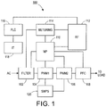
- FIG. 1 illustrates a high level block diagram of one embodiment of an AC to AC converter circuit 100.
- the circuit 100 includes an optional filter 102, a first pulse width modulation module (PWM1) 104, a second PWM2 106, a power factor controller (PFC) module 108, a microprocessor (MP) 110, a radio frequency (RF) communication module 112, a metering module 114, a power line communication (PLC) 116, an isolation transformer (IT) 118 and a switch mode power supply (SMPS) 120.
- PWM1 pulse width modulation module
- PFC power factor controller
- MP microprocessor
- RF radio frequency
- metering module 114
- PLC power line communication
- I isolation transformer
- SMPS switch mode power supply
- the RF communication module 112, the PLC module 116 and the IT 118 provide remote control by one of various network protocols.
- control signals may be sent from a remotely located control server over a wired or wireless connection via a wide area network (WAN).
- WAN wide area network
- the operation of the light source or brightness of a light source may be controlled remotely via the RF communication module 112 or the PLC module 116.
- the metering module 114 may be a module or device capable of monitoring a voltage level and a current level in the circuit. In one embodiment, the metering module 114 may be deployed as a metering system on a chip (M-SOC), multiple M-SOCs, an external metering module in communication with the MP 110, a sensor array with raw data input and the like. The metering module 114 may provide the voltage level and the current level to the MP 110.
- M-SOC metering system on a chip
- the MP 110 may use the measured voltage level and the current level to send control signals to the PWM2 106 and/or the PFC 108 to adjust the voltage level to change the intensity level or a level of light output of the AC powered light source. This is discussed in further detail below.
- the SMPS 120 may be an isolated SMPS.
- the SMPS may convert the AC power to DC power to operate and power various devices and modules within the circuit 100.
- the SMPS is not used to convert the AC power to DC power that is delivered to the light source.
- the filter 102 uses a combination of capacitance, resistance and inductance to filter destructive harmonic wave forms or switching noise in the circuit 100.
- the filter 102 may be controlled by the combination of feed forward and feedback circuits to effectively adapt the changing load and line conditions by adding or subtracting inductance, capacitance or resistance in any number of circuit configurations. The adjustments may be controlled by the microprocessor 110.
- the filter 102 may be a dynamic filter. In other words, the filter 102 may be configured to change the levels for which the destructive harmonic wave forms or switching noise are filtered out. In another embodiment, the filter 102 may be static. In other words, the filter 102 may be set for a worst case scenario without any adjustments in response to the changing load and line conditions.
- the PWM1 104 may perform voltage boost functions.
- the PWM1 104 may be controlled by the PFC 108 via feed forward and feedback loops.
- the PWM1 104 may be operated based upon a variable power level detected from the PWM2 106.
- the PWM1 104 operates in a variety of circuit configurations to perform the operation of boosting the line voltage.
- the PWM1 104 enables the power to be delivered to the load at the variable power level and a variable voltage level that can be adjustable in a disjoint or independent manner.
- the PWM2 106 may adjust a filtered AC power by altering a duty cycle or frequency of a chopped PWM AC sine wave.
- the PWM2 106 may operate in two stages. In the first stage, the PWM2 106 may feed power to a load. In the second stage, the PWM2 may interrupt the current path imposing a dead time creating an open circuit condition. The dead time provides a freewheeling safe commutation path complementary to the load for reactive inductive loads. This freewheeling circuitry bridge-less circuitry establishes a path for the commutation current for eliminating the destructive voltage spikes in the switches without the power losses of convention snubber circuits.
- the operation of the PWM1 104 and the PWM2 106 as controlled by the PFC 108 and the MP 110, respectively, alters the AC power input to produce a desired current output.
- the output voltage can be proportional to a lower current output or can be boosted by the PWM2 106.
- control signals from the MP 110 may be adapted to the changing desired voltage and current levels to provide a regulated linearly adjustable power source for a variety of loads both resistive and inductive in conjunction with the feedback from the PFC module 108.
- the MP 110 can continuously change the control signals sent to the PFC module 108 and the PWM2 104 based upon the changing voltage and current levels in the circuit 100 and the desired light output or desired intensity level.
- the PFC module 108 may continuously change the control signals sent to the PWM1 106 to adjust the line voltage.
- control of various loads in many cases may be customized for the correct operation of the individual load. This may be accomplished through the start procedure in unison to and with the feed-forward, feedback response and predetermined values stored in the MP 110. Furthermore, the MP 110 can be enhanced with additional storage capability and can then adapt to an even wider range of products.
- FIG. 2 illustrates a more detailed diagram of one embodiment of the example AC to AC converter circuit 100.
- the PWM1 104 illustrated by dashed lines may comprise a switch S1, a switch S2 and one or more inductors 204 and 206.
- the switches S1 and S2 may be one or more boost switches.
- the inductors 204 and 206 may store voltage that may be eventually released to the PWM2 106 as the switches S1 and S2 are activated.
- the two switches S1 and S2 are provided to operate in alternating fashion depending on a direction of the AC wave signal or sine wave.
- the switch S1 may operate during a first portion of the AC wave signal and the switch S2 may operate during a second portion of the AC wave signal as controlled by the PFC module 108 in accordance with a desired power output.
- the duty cycle or frequency of the switches S1 and S2 may be based upon control signals sent from the PFC module 108.
- a duty cycle may be defined as a time period for one on cycle and one off cycle.
- the frequency may be defined as how many duty cycles occur within a predefined period of time (e.g., 5 duty cycles per second).
- the PWM2 106 illustrated by dashed lines may comprise switches S3, S4, S5, S6 and S7.
- the switches S3 and S6 may be one or more load switches.
- the switches S4 and S5 grouped by dashed lines 210 may be one or more commutation switches.
- the switches S3, S4, S5 and S6 are driven by a driver 202.
- the load switches S3 and S6 and the commutation switches S4 and S5 may be operated and controlled by the MP 110.
- the MP 110 may control the duty cycle or frequency of the load switches S3 and S6 based upon a desired power output or an amount of power that is to be delivered to a load 208.
- the MP 110 may send a control signal 218 (e.g., a PWM signal) containing the appropriate duty cycle or frequency to the driver 202.
- the MP 110 may operate and activate the commutation switches S4 and S5 to re-circulate voltage left in the load 208 to avoid harmful voltage spikes.
- the switch S7 may be controlled by the MP 110 to regulate the voltage level via the PFC module 108.
- the MP 110 may send a control signal 214 (e.g., a PWM signal) containing the appropriate duty cycle or frequency to the switch S7.
- the switch S7 may receive feedback via a feedback signal 216. Operation of the switch S7 is discussed by example below.
- the control signal 214 and 218 sent by the MP 110 may be based upon a current level and a voltage level of the circuit 100 measured by a current sense resistor 212.
- the current sense resistor 212 may be coupled to the metering module 114 (e.g., illustrated as M-SOC 114 in FIG. 2 ).
- the metering module 114 may continuously monitor the current level and the voltage level measured by the current sense resistor 212 and provide the information to the MP 110 to calculate the necessary duty cycles for operating the switches S3, S6 and S7.
- the filter 102 illustrated by dashed lines may comprise a switch S8 and a switch S9. If the filter 102 is a dynamic filter, the switches S8 and S9 may operate at a duty cycle that is proportional to the desired light output or intensity level. The level of switching noise that is filtered out may change as the desired power output changes. In another embodiment, if the filter 102 is a static filter, the level of filtering may be set at a worst case scenario level.
- switches may be deployed. For example, depending on the application, more or less switches may be deployed. In addition, depending on how each module is configured, for example the PWM1 104, the PWM2 106 and the filter 102, more or less switches may be deployed.
- circuit 100 may be implemented using any suitable circuitry.
- slight modifications may be made to the circuit 100 to achieve the same functions discussed herein that are still within the scope of the present disclosure.
- present disclosure encompasses the use of additional feedback circuits or feed forward circuits between various modules within the circuit depending on a particular application.
- the load 208 e.g., a light source, a street light fixture, an LED based street light fixture, and the like
- the MP 110 may send a control signal 218 to the driver 202 to keep the switches S3 and S6 in an on state 100% of the time.
- the MP 110 may also send a control signal 214 to the switch S7 to maintain the switch S7 on a mostly on state. In other words, the switch S7 may be operating on a extremely low duty cycle.
- a control signal may be sent to the MP 110 from a remote server that instructs circuit 100 to operate the load 208 at 50% intensity or light output.
- the control signal may be received by the PLC module 116 or wirelessly over the RF communication module 112.
- the MP 110 may send a control signal 218 to the driver 202 to operate the switches S3 and S6 at a 50% duty cycle. However, such operation may cause a drop in voltage across the load.
- the current sense resistor 212 may measure the current level and the voltage level in the circuit 100.
- the metering module 114 may provide the measured current level and voltage level to the MP 110.
- the MP 110 may determine if the load 208 is operating in an optimal voltage or non-optimal voltage. If the load 208 is not operating at an optimal voltage, the MP 110 may determine how much the voltage level (e.g., an outgoing voltage level) must be adjusted (e.g., more or less) to operate the load 208 at an optimal voltage.
- an operating profile or dimming curve profile of the load 208 e.g., a current vs. voltage profile of a light source
- the MP 110 may determine if the load 208 is operating in an optimal voltage or non-optimal voltage. If the load 208 is not operating at an optimal voltage, the MP 110 may determine how much the voltage level (e.g., an outgoing voltage level) must be adjusted (e.g., more or less) to operate the load 208 at an optimal voltage.
- the MP 110 may send a control signal 214 to the switch S7 to operate a specified duty cycle to obtain a proper voltage adjustment.
- the PFC module 108 may detect the duty cycle of the switch S7 and respond by operating the switches S1 and S2 at a duty cycle in as a function of an operation of the switch S7. For example, the switches S1 and S2 may be operated proportional to the duty cycle the switch S7. The operation of the switches S1 and S2 adjust the voltage which is supplied by the switches S3 and S6.
- the current sense resistor 212 may measure the updated current level and updated voltage level.
- the metering module 114 may provide this information to the MP 110 and if the load 208 is not operating in an optimal state for 50% intensity or light output, the entire process may be repeated until the load 208 is operating at an optimal state.
- V o may represent an output voltage
- V i may represent an input voltage
- V t may represent a target output voltage
- V d may represent a change in voltage for 1% duty cycle change
- V n may represent a difference between original input voltage and target voltage.
- the target output voltage V t may be set to a desired value based upon the operating profile of the load 208.
- the AC power supply may be turned on and the algorithm may operate as follows:
- switches S3 and S6 When a dimming control signal is received to adjust the intensity or light output of the load 208 the switches S3 and S6 may be manipulated to achieve the desired dimming level. Then the steps 1-5 above may be repeated.
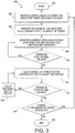
- FIG. 3 illustrates an example flowchart of one embodiment of a method 300 for automatically controlling an impedance of a circuit.
- the steps, functions, or operations of the method 300 may be performed by the MP 110 in the AC to AC converter circuit 100 or a general purpose computer illustrated in FIG. 4 and discussed below.
- the method 300 begins at step 302.
- the method 300 receives a control signal to change an amount of power delivered to a light.
- the control signal may be received, over either a wired connection or a wireless connection, from a remote or centralized control server over a WAN network via a PLC module or an RF communications module.
- the control signal may be to change an intensity level or a light output level of the light, e.g., from 100% to 50%. As a result, the amount of power delivered to the light may be reduced by 50%.
- the method 300 operates one or more load switches in accordance with the amount of power.
- the MP may send a control signal to the driver of one or more load switches (e.g., switches S3 and S6 in FIG. 2 ) to operate the one or more load switches in accordance with the desired power output.
- the load switches may be operated at a 50% duty cycle to reduce the amount of power by 50%.
- the method 300 monitors a current level and a voltage level while the one or more load switches are operating.
- a current sense resistor may be used to measure a current level and a voltage level in the circuit.
- the current level e.g., an output current to the load
- voltage level e.g., an output voltage to the load
- the method 300 determines if the light is operating at an optimal voltage. For example, if the measured voltage level is equal to or within a predefined threshold of the target voltage (e.g., +/- 5%), the MP may determine that the light is operating at an optimal voltage. If the answer to step 310 is yes, the method 300 may then return to step 308 to continue monitoring the current level and the voltage level.
- a predefined threshold of the target voltage e.g., +/- 5%
- the method 300 may proceed to step 312.
- the method 300 may send a signal to a PFC to adjust the voltage.
- the percentage change in duty cycle may be calculated based upon the algorithm discussed above.
- the change in duty cycle may then be sent to a switch coupled to the PFC and the MP (e.g., the switch S7 in FIG. 2 ) to operate the switch in accordance with a desired power output.
- the duty cycle may be adjusted to obtain the needed target voltage.
- the PFC may then modify the operation of one or more boost switches (e.g., switches S1 and S2 in FIG. 2 ) to adjust the voltage as a function of an operation of the switch coupled to the PFC and the MP.
- the boost switches may either provide more or less voltage depending on the amount of power to be delivered to the light and the change in duty cycle of the switch coupled to the PFC and the MP.
- the method 300 may determine if the light is operating at an optimal voltage. Similar to step 310 for example, if the measured voltage level is equal to or within a predefined threshold of the target voltage (e.g., +/- 5%), the MP may determine that the light is operating at an optimal voltage. At step 314 if the answer to step 314 is no, the method 300 may proceed to step 316.
- a predefined threshold of the target voltage e.g., +/- 5%
- the method 300 adjusts the control signal sent to the PFC.
- the MP may calculate the additional change in duty cycle needed to operate the switch coupled to the PFC and the MP to obtain the needed target voltage. The method 300 then proceeds to step 312 again.
- step 318 the method 300 determines if there is a change in the amount of power requested. For example, the central controller or server may send a control signal to the MP to increase the intensity of the light back to 100% from 50%.
- step 318 If the answer to step 318 is yes, the method 300 may proceed to step 304. However, if the answer to step 318 is no, the method 300 may proceed to step 320. The method 300 ends at step 320.
- one or more steps or operations of the method 300 described above may include a storing, displaying and/or outputting step as required for a particular application.
- any data, records, fields, and/or intermediate results discussed in the methods can be stored, displayed, and/or outputted to another device as required for a particular application.
- steps, operations or blocks in FIG. 3 that recite a determining operation, or involve a decision do not necessarily require that both branches of the determining operation be practiced. In other words, one of the branches of the determining operation can be deemed as an optional step.
- operations, steps or blocks of the above described methods can be combined, separated, and/or performed in a different order from that described above, without departing from the example embodiments of the present disclosure.
- FIG. 4 depicts a high-level block diagram of a general-purpose computer suitable for use in performing the functions described herein.
- the system 400 comprises a hardware processor element 402 (e.g., a CPU), a memory 404, e.g., random access memory (RAM) and/or read only memory (ROM), a module 405 for adjusting a light output of a light operating on alternating current (AC) power, and various input/output devices 406, e.g., a camera, a video camera, storage devices, including but not limited to, a tape drive, a floppy drive, a hard disk drive or a compact disk drive, a receiver, a transmitter, a speaker, a display, a speech synthesizer, an output port, and a user input device (such as a keyboard, a keypad, a mouse, and the like).
- a hardware processor element 402 e.g., a CPU
- memory 404 e.g., random access memory (RAM) and/
- the present disclosure can be implemented in software and/or in a combination of software and hardware, e.g., using application specific integrated circuits (ASIC), a general purpose computer or any other hardware equivalents, e.g., computer readable instructions pertaining to the method(s) discussed above can be used to configure a hardware processor to perform the steps functions and/or operations of the above disclosed methods.
- the present module or process 405 for adjusting a light output of a light operating on alternating current (AC) power can be implemented as computer-executable instructions (e.g., a software program comprising computer-executable instructions) and loaded into memory 404 and executed by hardware processor 402 to implement the functions as discussed above.
- the present method 405 for adjusting a light output of a light operating on alternating current (AC) power as discussed above in method 300 (including associated data structures) of the present disclosure can be stored on a non-transitory (e.g., tangible or physical) computer readable storage medium, e.g., RAM memory, magnetic or optical drive or diskette and the like.
- a non-transitory e.g., tangible or physical
- computer readable storage medium e.g., RAM memory, magnetic or optical drive or diskette and the like.
Claims (15)
- Circuit de convertisseur de courant alternatif à courant alternatif, CA-CA, (100), pour ajuster indépendamment une intensité et une tension en vue d'ajuster une sortie de lumière d'une lumière fonctionnant sur courant alternatif, comprenant :un microprocesseur (110) ; etun premier commutateur (S7) couplé au microprocesseur (110) en vue de recevoir un premier signal de commande (214) en provenance du microprocesseur ;caractérisé en ce que ledit circuit de convertisseur comporte en outre :un module de contrôleur de facteur de puissance (PFC) (108) couplé au premier commutateur, dans lequel le premier commutateur est commandé par le microprocesseur (110) selon le premier signal de commande en vue de réguler une sortie de puissance souhaitée par l'intermédiaire du module de contrôleur PFC ;un ou plusieurs commutateurs-amplificateurs (S1, S2) couplés au module de contrôleur PFC (108) en vue de recevoir des signaux de commande respectifs en provenance du module de contrôleur PFC, dans lequel ledit un ou lesdits plusieurs commutateurs-amplificateurs (S1, S2) sont commandés par le module de contrôleur PFC (108) en fonction d'une opération du premier commutateur visant à ajuster un niveau de tension ; etun ou plusieurs commutateurs de charge (S3, S6) couplés audit un ou auxdits plusieurs commutateurs-amplificateurs (S1, S2), dans lequel ledit un ou lesdits plusieurs commutateurs de charge (S3, S6) reçoivent ledit niveau de tension et sont commandés par le microprocesseur (110) selon la sortie de puissance souhaitée.
- Circuit de convertisseur CA-CA selon la revendication 1, comprenant en outre :un module de mesure couplé au microprocesseur (110), dans lequel le module de mesure surveille un niveau d'intensité et un niveau de tension et fournit le niveau d'intensité et le niveau de tension au microprocesseur (110).
- Circuit de convertisseur CA-CA selon la revendication 2, comprenant en outre :une résistance couplée au module de mesure en vue de mesurer le niveau d'intensité.
- Circuit de convertisseur CA-CA selon la revendication 1, comprenant en outre :un filtre couplé au module de contrôleur PFC (108) et audit un ou auxdits plusieurs commutateurs de charge (S3, S6).
- Circuit de convertisseur CA-CA selon la revendication 4, dans lequel le filtre est un filtre dynamique.
- Circuit de convertisseur CA-CA selon la revendication 4, dans lequel le filtre est un filtre statique.
- Circuit de convertisseur CA-CA selon la revendication 1, comprenant en outre :un ou plusieurs modules de communication couplés au microprocesseur (110).
- Circuit de convertisseur CA-CA selon la revendication 7, dans lequel ledit un ou lesdits plusieurs modules de communication comportent au moins l'un parmi : un module de communication par ligne électrique (PLC) ou un module de communication radiofréquence (RF).
- Circuit de convertisseur CA-CA selon la revendication 1, dans lequel ledit un ou lesdits plusieurs commutateurs-amplificateurs (S1, S2) comportent un premier commutateur-amplificateur et un second commutateur-amplificateur, dans lequel le premier commutateur-amplificateur fonctionne au cours d'une première partie d'un signal d'onde CA et le second commutateur-amplificateur fonctionne au cours d'une seconde partie du signal d'onde CA, tel que commandé par le module de contrôleur PFC (108) selon la sortie de puissance souhaitée.
- Circuit de convertisseur CA-CA selon la revendication 1, comprenant en outre :un ou plusieurs commutateurs de communication couplés audit un ou auxdits plusieurs commutateurs de charge (S3, S6).
- Procédé d'ajustement d'une sortie de lumière d'une lumière fonctionnant sur courant alternatif (CA), comprenant l'étape ci-dessous consistant à :recevoir, au niveau d'un microprocesseur, un signal de commande en provenance d'un serveur de commande distant, visant à modifier une quantité de puissance délivrée à la lumière, dans lequel la puissance est délivrée par une source de courant alternatif ;ledit procédé étant caractérisé en ce qu'il comporte en outre les étapes ci-dessous consistant à :exploiter un pilote couplé à un ou plusieurs commutateurs de charge (S3, S6) en réponse au signal de commande, en vue d'exploiter ledit un ou lesdits plusieurs commutateurs de charge selon la quantité de puissance ;surveiller un niveau d'intensité et un niveau de tension par le biais d'une résistance de détection de courant tandis que ledit un ou lesdits plusieurs commutateurs de charge (S3, S6) fonctionnent ; etenvoyer un signal à un commutateur couplé à un module de contrôleur de facteur de puissance (PFC) (108) si la lumière fonctionne à un niveau de tension non optimal, et commander ledit commutateur par le biais dudit microprocesseur, dans lequel le contrôleur PFC (108) est couplé à un ou plusieurs commutateurs-amplificateurs et ajuste le niveau de tension délivré par ledit un ou lesdits plusieurs commutateurs de charge par le biais d'une commande dudit un ou desdits plusieurs commutateurs-amplificateurs selon une opération du commutateur.
- Procédé selon la revendication 11, dans lequel le signal comporte un signal de modulation d'impulsion en durée (PWM).
- Procédé selon la revendication 12, dans lequel le signal de modulation PWM détermine un premier cycle de service du commutateur couplé au module de contrôleur PFC (108), dans lequel le premier cycle de service est déterminé sur la base d'une augmentation du niveau de tension qui est nécessaire en vue d'exploiter la lumière à un niveau de tension optimal.
- Procédé selon la revendication 13, dans lequel le contrôleur PFC (108) ajuste le niveau de tension selon l'opération du commutateur en exploitant un premier commutateur-amplificateur et un second commutateur-amplificateur à un second cycle de service, dans lequel le second cycle de service est déterminé sur la base de l'augmentation du niveau de tension qui est nécessaire en vue d'exploiter la lumière au niveau de tension optimal.
- Procédé selon la revendication 11, comprenant en outre l'étape ci-dessous consistant à :surveiller le niveau d'intensité et le niveau de tension, une fois le niveau de tension ajusté par le module de contrôleur PFC (108), en vue de déterminer si le signal envoyé au module de contrôleur PFC (108) doit être ajusté.
Applications Claiming Priority (2)
| Application Number | Priority Date | Filing Date | Title |
|---|---|---|---|
| US201261593413P | 2012-02-01 | 2012-02-01 | |
| PCT/US2013/023907 WO2013116374A1 (fr) | 2012-02-01 | 2013-01-30 | Convertisseur ca-ca à intensité et tension réglables indépendamment |
Publications (3)
| Publication Number | Publication Date |
|---|---|
| EP2810364A1 EP2810364A1 (fr) | 2014-12-10 |
| EP2810364A4 EP2810364A4 (fr) | 2016-03-23 |
| EP2810364B1 true EP2810364B1 (fr) | 2017-07-12 |
Family
ID=48869638
Family Applications (1)
| Application Number | Title | Priority Date | Filing Date |
|---|---|---|---|
| EP13743958.4A Active EP2810364B1 (fr) | 2012-02-01 | 2013-01-30 | Convertisseur ca-ca à intensité et tension réglables indépendamment |
Country Status (7)
| Country | Link |
|---|---|
| US (2) | US9380676B2 (fr) |
| EP (1) | EP2810364B1 (fr) |
| AU (1) | AU2013215245B2 (fr) |
| BR (1) | BR112014019143A8 (fr) |
| CA (1) | CA2863592C (fr) |
| TW (1) | TW201351864A (fr) |
| WO (1) | WO2013116374A1 (fr) |
Families Citing this family (6)
| Publication number | Priority date | Publication date | Assignee | Title |
|---|---|---|---|---|
| US9380676B2 (en) * | 2012-02-01 | 2016-06-28 | Dialight Corporation | Independently adjustable current and voltage AC-AC converter |
| US9693428B2 (en) | 2014-10-15 | 2017-06-27 | Abl Ip Holding Llc | Lighting control with automated activation process |
| US9781814B2 (en) | 2014-10-15 | 2017-10-03 | Abl Ip Holding Llc | Lighting control with integral dimming |
| US9829899B2 (en) | 2014-11-10 | 2017-11-28 | Duke Energy Corporation | Apparatuses including utility meter, power electronics, and communications circuitry, and related methods of operation |
| CN108509372B (zh) * | 2018-02-27 | 2022-04-01 | 晶晨半导体(上海)股份有限公司 | 一种片上系统芯片 |
| EP3847433B1 (fr) | 2018-09-04 | 2023-07-05 | SeeScan, Inc. | Systèmes d'inspection vidéo de canalisation par vidéo auxquels sont intégrées des données de capteurs supplémentaires |
Family Cites Families (14)
| Publication number | Priority date | Publication date | Assignee | Title |
|---|---|---|---|---|
| SG44798A1 (en) * | 1994-02-10 | 1997-12-19 | Philips Electronics Nv | High frequency ac/ac converter with power factor correction |
| JPH11500861A (ja) * | 1995-12-08 | 1999-01-19 | フィリップス、エレクトロニクス、ネムローゼ、フェンノートシャップ | バラスト・システム |
| US6346778B1 (en) | 1998-01-20 | 2002-02-12 | Bytecraft Pty Ltd | AC power converter |
| US6963178B1 (en) * | 1998-12-07 | 2005-11-08 | Systel Development And Industries Ltd. | Apparatus for controlling operation of gas discharge devices |
| US6525490B1 (en) | 2000-10-02 | 2003-02-25 | Patricia Ann Bailey | Power saving circuitry |
| US7009348B2 (en) * | 2002-06-03 | 2006-03-07 | Systel Development & Industries Ltd. | Multiple channel ballast and networkable topology and system including power line carrier applications |
| US7906872B2 (en) * | 2005-12-20 | 2011-03-15 | Crompton Greaves Limited | Dynamic harmonic filter for an AC power system |
| US7310254B2 (en) * | 2006-02-15 | 2007-12-18 | Rockwell Automation Technologies, Inc. | AC-to-AC (frequency) converter with three switches per leg |
| WO2008156015A1 (fr) * | 2007-06-20 | 2008-12-24 | Panasonic Electric Works Co., Ltd. | Dispositif de commande d'une lampe à décharge, dispositif d'éclairage, et dispositif d'affichage à cristaux liquides |
| TW201024591A (en) | 2008-12-31 | 2010-07-01 | Ind Tech Res Inst | Lamps module |
| US8084949B2 (en) | 2009-07-09 | 2011-12-27 | General Electric Company | Fluorescent ballast with inherent end-of-life protection |
| US8288958B2 (en) * | 2010-02-16 | 2012-10-16 | Vito Rinaldi | Dynamic application of cut-out pulses in alternating current power |
| TWM412313U (en) | 2011-03-04 | 2011-09-21 | Wen-Wang Ke | Energy-saving control device of illumination circuit of LED lamp |
| US9380676B2 (en) * | 2012-02-01 | 2016-06-28 | Dialight Corporation | Independently adjustable current and voltage AC-AC converter |
-
2013
- 2013-01-30 US US13/754,321 patent/US9380676B2/en active Active
- 2013-01-30 EP EP13743958.4A patent/EP2810364B1/fr active Active
- 2013-01-30 WO PCT/US2013/023907 patent/WO2013116374A1/fr active Application Filing
- 2013-01-30 CA CA2863592A patent/CA2863592C/fr active Active
- 2013-01-30 AU AU2013215245A patent/AU2013215245B2/en active Active
- 2013-01-30 BR BR112014019143A patent/BR112014019143A8/pt not_active IP Right Cessation
- 2013-01-31 TW TW102103761A patent/TW201351864A/zh unknown
-
2016
- 2016-06-27 US US15/193,758 patent/US9967951B2/en active Active
Non-Patent Citations (1)
| Title |
|---|
| None * |
Also Published As
| Publication number | Publication date |
|---|---|
| EP2810364A4 (fr) | 2016-03-23 |
| EP2810364A1 (fr) | 2014-12-10 |
| US20160309563A1 (en) | 2016-10-20 |
| BR112014019143A2 (fr) | 2017-06-20 |
| CA2863592C (fr) | 2017-01-10 |
| US9380676B2 (en) | 2016-06-28 |
| US9967951B2 (en) | 2018-05-08 |
| TW201351864A (zh) | 2013-12-16 |
| AU2013215245B2 (en) | 2017-06-01 |
| CA2863592A1 (fr) | 2013-08-08 |
| WO2013116374A1 (fr) | 2013-08-08 |
| AU2013215245A1 (en) | 2014-08-28 |
| US20130193868A1 (en) | 2013-08-01 |
| BR112014019143A8 (pt) | 2017-07-11 |
Similar Documents
| Publication | Publication Date | Title |
|---|---|---|
| US9967951B2 (en) | Independently adjustable current and voltage AC-AC converter | |
| TWI528856B (zh) | Led調光驅動器 | |
| US8294388B2 (en) | Driving system with inductor pre-charging for LED systems with PWM dimming control or other loads | |
| US20150312981A1 (en) | Current adjusting device and adjustment method thereof | |
| US8872438B2 (en) | LED light dimming with a target brightness | |
| US9681503B2 (en) | Transformer for a lamp, LED converter, and transformer operation method | |
| CN103582239B (zh) | 调光控制器、光源驱动电路及控制光源调光的方法 | |
| US20100141178A1 (en) | Dimmer control leakage pull down using main power device in flyback converter | |
| US20100141173A1 (en) | Linearity in led dimmer control | |
| US9320103B2 (en) | Light-emitting diode (LED) driver, LED lighting apparatus, and method of operating LED lighting apparatus | |
| US20130241433A1 (en) | Method, apparatus and system for controlling light source | |
| US9693411B1 (en) | LED driver configuration and dimming interface for dynamic adjustment of driver operating parameters | |
| CN104640300A (zh) | 光源驱动电路、色温控制器及控制光源色温的方法 | |
| US20130214756A1 (en) | Wide input voltage range power factor correction circuit | |
| JP6704911B2 (ja) | ドライバ回路及び方法 | |
| EP2519080B1 (fr) | Appareil et procédé d'éclairage | |
| EP3560086B1 (fr) | Convertisseur synchrone | |
| US9648678B1 (en) | LED driver circuit with dimming control and programming interfaces | |
| US9629209B1 (en) | Offline tuning interface for LED drivers | |
| EP3076758B1 (fr) | Optimisation d'allumage | |
| CN110168837A (zh) | 包括电力备用装置的照明系统 | |
| CN111096077B (zh) | 用于电气负载的操作设备和方法 | |
| US9386645B2 (en) | LED drive circuitry with disconnect switch | |
| US10015867B2 (en) | Low-voltage controller with dimming function and method | |
| US9420665B2 (en) | Systems and methods for continuous adjustment of reference signal to control chip |
Legal Events
| Date | Code | Title | Description |
|---|---|---|---|
| PUAI | Public reference made under article 153(3) epc to a published international application that has entered the european phase |
Free format text: ORIGINAL CODE: 0009012 |
|
| 17P | Request for examination filed |
Effective date: 20140821 |
|
| AK | Designated contracting states |
Kind code of ref document: A1 Designated state(s): AL AT BE BG CH CY CZ DE DK EE ES FI FR GB GR HR HU IE IS IT LI LT LU LV MC MK MT NL NO PL PT RO RS SE SI SK SM TR |
|
| AX | Request for extension of the european patent |
Extension state: BA ME |
|
| DAX | Request for extension of the european patent (deleted) | ||
| RA4 | Supplementary search report drawn up and despatched (corrected) |
Effective date: 20160224 |
|
| RIC1 | Information provided on ipc code assigned before grant |
Ipc: H02M 5/00 20060101AFI20160218BHEP Ipc: H05B 37/02 20060101ALI20160218BHEP Ipc: H02M 5/275 20060101ALI20160218BHEP |
|
| STAA | Information on the status of an ep patent application or granted ep patent |
Free format text: STATUS: EXAMINATION IS IN PROGRESS |
|
| RIC1 | Information provided on ipc code assigned before grant |
Ipc: H02M 5/00 20060101AFI20161025BHEP Ipc: H05B 37/02 20060101ALI20161025BHEP Ipc: H02M 5/275 20060101ALI20161025BHEP |
|
| 17Q | First examination report despatched |
Effective date: 20161125 |
|
| GRAJ | Information related to disapproval of communication of intention to grant by the applicant or resumption of examination proceedings by the epo deleted |
Free format text: ORIGINAL CODE: EPIDOSDIGR1 |
|
| GRAP | Despatch of communication of intention to grant a patent |
Free format text: ORIGINAL CODE: EPIDOSNIGR1 |
|
| GRAP | Despatch of communication of intention to grant a patent |
Free format text: ORIGINAL CODE: EPIDOSNIGR1 |
|
| STAA | Information on the status of an ep patent application or granted ep patent |
Free format text: STATUS: GRANT OF PATENT IS INTENDED |
|
| INTG | Intention to grant announced |
Effective date: 20170208 |
|
| GRAS | Grant fee paid |
Free format text: ORIGINAL CODE: EPIDOSNIGR3 |
|
| GRAA | (expected) grant |
Free format text: ORIGINAL CODE: 0009210 |
|
| STAA | Information on the status of an ep patent application or granted ep patent |
Free format text: STATUS: THE PATENT HAS BEEN GRANTED |
|
| AK | Designated contracting states |
Kind code of ref document: B1 Designated state(s): AL AT BE BG CH CY CZ DE DK EE ES FI FR GB GR HR HU IE IS IT LI LT LU LV MC MK MT NL NO PL PT RO RS SE SI SK SM TR |
|
| REG | Reference to a national code |
Ref country code: GB Ref legal event code: FG4D |
|
| REG | Reference to a national code |
Ref country code: CH Ref legal event code: EP |
|
| REG | Reference to a national code |
Ref country code: AT Ref legal event code: REF Ref document number: 909195 Country of ref document: AT Kind code of ref document: T Effective date: 20170715 |
|
| REG | Reference to a national code |
Ref country code: IE Ref legal event code: FG4D |
|
| REG | Reference to a national code |
Ref country code: DE Ref legal event code: R096 Ref document number: 602013023434 Country of ref document: DE |
|
| REG | Reference to a national code |
Ref country code: NL Ref legal event code: MP Effective date: 20170712 |
|
| REG | Reference to a national code |
Ref country code: LT Ref legal event code: MG4D |
|
| REG | Reference to a national code |
Ref country code: AT Ref legal event code: MK05 Ref document number: 909195 Country of ref document: AT Kind code of ref document: T Effective date: 20170712 |
|
| REG | Reference to a national code |
Ref country code: FR Ref legal event code: PLFP Year of fee payment: 6 |
|
| PG25 | Lapsed in a contracting state [announced via postgrant information from national office to epo] |
Ref country code: HR Free format text: LAPSE BECAUSE OF FAILURE TO SUBMIT A TRANSLATION OF THE DESCRIPTION OR TO PAY THE FEE WITHIN THE PRESCRIBED TIME-LIMIT Effective date: 20170712 Ref country code: NL Free format text: LAPSE BECAUSE OF FAILURE TO SUBMIT A TRANSLATION OF THE DESCRIPTION OR TO PAY THE FEE WITHIN THE PRESCRIBED TIME-LIMIT Effective date: 20170712 Ref country code: LT Free format text: LAPSE BECAUSE OF FAILURE TO SUBMIT A TRANSLATION OF THE DESCRIPTION OR TO PAY THE FEE WITHIN THE PRESCRIBED TIME-LIMIT Effective date: 20170712 Ref country code: FI Free format text: LAPSE BECAUSE OF FAILURE TO SUBMIT A TRANSLATION OF THE DESCRIPTION OR TO PAY THE FEE WITHIN THE PRESCRIBED TIME-LIMIT Effective date: 20170712 Ref country code: NO Free format text: LAPSE BECAUSE OF FAILURE TO SUBMIT A TRANSLATION OF THE DESCRIPTION OR TO PAY THE FEE WITHIN THE PRESCRIBED TIME-LIMIT Effective date: 20171012 Ref country code: SE Free format text: LAPSE BECAUSE OF FAILURE TO SUBMIT A TRANSLATION OF THE DESCRIPTION OR TO PAY THE FEE WITHIN THE PRESCRIBED TIME-LIMIT Effective date: 20170712 Ref country code: AT Free format text: LAPSE BECAUSE OF FAILURE TO SUBMIT A TRANSLATION OF THE DESCRIPTION OR TO PAY THE FEE WITHIN THE PRESCRIBED TIME-LIMIT Effective date: 20170712 |
|
| PG25 | Lapsed in a contracting state [announced via postgrant information from national office to epo] |
Ref country code: GR Free format text: LAPSE BECAUSE OF FAILURE TO SUBMIT A TRANSLATION OF THE DESCRIPTION OR TO PAY THE FEE WITHIN THE PRESCRIBED TIME-LIMIT Effective date: 20171013 Ref country code: RS Free format text: LAPSE BECAUSE OF FAILURE TO SUBMIT A TRANSLATION OF THE DESCRIPTION OR TO PAY THE FEE WITHIN THE PRESCRIBED TIME-LIMIT Effective date: 20170712 Ref country code: BG Free format text: LAPSE BECAUSE OF FAILURE TO SUBMIT A TRANSLATION OF THE DESCRIPTION OR TO PAY THE FEE WITHIN THE PRESCRIBED TIME-LIMIT Effective date: 20171012 Ref country code: IS Free format text: LAPSE BECAUSE OF FAILURE TO SUBMIT A TRANSLATION OF THE DESCRIPTION OR TO PAY THE FEE WITHIN THE PRESCRIBED TIME-LIMIT Effective date: 20171112 Ref country code: LV Free format text: LAPSE BECAUSE OF FAILURE TO SUBMIT A TRANSLATION OF THE DESCRIPTION OR TO PAY THE FEE WITHIN THE PRESCRIBED TIME-LIMIT Effective date: 20170712 Ref country code: PL Free format text: LAPSE BECAUSE OF FAILURE TO SUBMIT A TRANSLATION OF THE DESCRIPTION OR TO PAY THE FEE WITHIN THE PRESCRIBED TIME-LIMIT Effective date: 20170712 Ref country code: ES Free format text: LAPSE BECAUSE OF FAILURE TO SUBMIT A TRANSLATION OF THE DESCRIPTION OR TO PAY THE FEE WITHIN THE PRESCRIBED TIME-LIMIT Effective date: 20170712 |
|
| REG | Reference to a national code |
Ref country code: DE Ref legal event code: R097 Ref document number: 602013023434 Country of ref document: DE |
|
| PG25 | Lapsed in a contracting state [announced via postgrant information from national office to epo] |
Ref country code: RO Free format text: LAPSE BECAUSE OF FAILURE TO SUBMIT A TRANSLATION OF THE DESCRIPTION OR TO PAY THE FEE WITHIN THE PRESCRIBED TIME-LIMIT Effective date: 20170712 Ref country code: CZ Free format text: LAPSE BECAUSE OF FAILURE TO SUBMIT A TRANSLATION OF THE DESCRIPTION OR TO PAY THE FEE WITHIN THE PRESCRIBED TIME-LIMIT Effective date: 20170712 Ref country code: DK Free format text: LAPSE BECAUSE OF FAILURE TO SUBMIT A TRANSLATION OF THE DESCRIPTION OR TO PAY THE FEE WITHIN THE PRESCRIBED TIME-LIMIT Effective date: 20170712 |
|
| PLBE | No opposition filed within time limit |
Free format text: ORIGINAL CODE: 0009261 |
|
| STAA | Information on the status of an ep patent application or granted ep patent |
Free format text: STATUS: NO OPPOSITION FILED WITHIN TIME LIMIT |
|
| PG25 | Lapsed in a contracting state [announced via postgrant information from national office to epo] |
Ref country code: SM Free format text: LAPSE BECAUSE OF FAILURE TO SUBMIT A TRANSLATION OF THE DESCRIPTION OR TO PAY THE FEE WITHIN THE PRESCRIBED TIME-LIMIT Effective date: 20170712 Ref country code: IT Free format text: LAPSE BECAUSE OF FAILURE TO SUBMIT A TRANSLATION OF THE DESCRIPTION OR TO PAY THE FEE WITHIN THE PRESCRIBED TIME-LIMIT Effective date: 20170712 Ref country code: SK Free format text: LAPSE BECAUSE OF FAILURE TO SUBMIT A TRANSLATION OF THE DESCRIPTION OR TO PAY THE FEE WITHIN THE PRESCRIBED TIME-LIMIT Effective date: 20170712 Ref country code: EE Free format text: LAPSE BECAUSE OF FAILURE TO SUBMIT A TRANSLATION OF THE DESCRIPTION OR TO PAY THE FEE WITHIN THE PRESCRIBED TIME-LIMIT Effective date: 20170712 |
|
| 26N | No opposition filed |
Effective date: 20180413 |
|
| PG25 | Lapsed in a contracting state [announced via postgrant information from national office to epo] |
Ref country code: SI Free format text: LAPSE BECAUSE OF FAILURE TO SUBMIT A TRANSLATION OF THE DESCRIPTION OR TO PAY THE FEE WITHIN THE PRESCRIBED TIME-LIMIT Effective date: 20170712 |
|
| REG | Reference to a national code |
Ref country code: CH Ref legal event code: PL |
|
| PG25 | Lapsed in a contracting state [announced via postgrant information from national office to epo] |
Ref country code: LU Free format text: LAPSE BECAUSE OF NON-PAYMENT OF DUE FEES Effective date: 20180130 |
|
| REG | Reference to a national code |
Ref country code: IE Ref legal event code: MM4A |
|
| REG | Reference to a national code |
Ref country code: BE Ref legal event code: MM Effective date: 20180131 |
|
| PG25 | Lapsed in a contracting state [announced via postgrant information from national office to epo] |
Ref country code: BE Free format text: LAPSE BECAUSE OF NON-PAYMENT OF DUE FEES Effective date: 20180131 Ref country code: LI Free format text: LAPSE BECAUSE OF NON-PAYMENT OF DUE FEES Effective date: 20180131 Ref country code: CH Free format text: LAPSE BECAUSE OF NON-PAYMENT OF DUE FEES Effective date: 20180131 |
|
| PG25 | Lapsed in a contracting state [announced via postgrant information from national office to epo] |
Ref country code: IE Free format text: LAPSE BECAUSE OF NON-PAYMENT OF DUE FEES Effective date: 20180130 |
|
| PG25 | Lapsed in a contracting state [announced via postgrant information from national office to epo] |
Ref country code: MC Free format text: LAPSE BECAUSE OF FAILURE TO SUBMIT A TRANSLATION OF THE DESCRIPTION OR TO PAY THE FEE WITHIN THE PRESCRIBED TIME-LIMIT Effective date: 20170712 |
|
| PG25 | Lapsed in a contracting state [announced via postgrant information from national office to epo] |
Ref country code: MT Free format text: LAPSE BECAUSE OF NON-PAYMENT OF DUE FEES Effective date: 20180130 |
|
| PG25 | Lapsed in a contracting state [announced via postgrant information from national office to epo] |
Ref country code: TR Free format text: LAPSE BECAUSE OF FAILURE TO SUBMIT A TRANSLATION OF THE DESCRIPTION OR TO PAY THE FEE WITHIN THE PRESCRIBED TIME-LIMIT Effective date: 20170712 |
|
| PG25 | Lapsed in a contracting state [announced via postgrant information from national office to epo] |
Ref country code: PT Free format text: LAPSE BECAUSE OF FAILURE TO SUBMIT A TRANSLATION OF THE DESCRIPTION OR TO PAY THE FEE WITHIN THE PRESCRIBED TIME-LIMIT Effective date: 20170712 Ref country code: HU Free format text: LAPSE BECAUSE OF FAILURE TO SUBMIT A TRANSLATION OF THE DESCRIPTION OR TO PAY THE FEE WITHIN THE PRESCRIBED TIME-LIMIT; INVALID AB INITIO Effective date: 20130130 |
|
| PG25 | Lapsed in a contracting state [announced via postgrant information from national office to epo] |
Ref country code: CY Free format text: LAPSE BECAUSE OF FAILURE TO SUBMIT A TRANSLATION OF THE DESCRIPTION OR TO PAY THE FEE WITHIN THE PRESCRIBED TIME-LIMIT Effective date: 20170712 Ref country code: MK Free format text: LAPSE BECAUSE OF NON-PAYMENT OF DUE FEES Effective date: 20170712 |
|
| PG25 | Lapsed in a contracting state [announced via postgrant information from national office to epo] |
Ref country code: AL Free format text: LAPSE BECAUSE OF FAILURE TO SUBMIT A TRANSLATION OF THE DESCRIPTION OR TO PAY THE FEE WITHIN THE PRESCRIBED TIME-LIMIT Effective date: 20170712 |
|
| PGFP | Annual fee paid to national office [announced via postgrant information from national office to epo] |
Ref country code: DE Payment date: 20221215 Year of fee payment: 11 |
|
| P01 | Opt-out of the competence of the unified patent court (upc) registered |
Effective date: 20230524 |
|
| PGFP | Annual fee paid to national office [announced via postgrant information from national office to epo] |
Ref country code: GB Payment date: 20231218 Year of fee payment: 12 |
|
| PGFP | Annual fee paid to national office [announced via postgrant information from national office to epo] |
Ref country code: FR Payment date: 20231214 Year of fee payment: 12 |