EP2808885B1 - Precursor for planar deprocessing of semiconductor devices using a focused ion beam - Google Patents
Precursor for planar deprocessing of semiconductor devices using a focused ion beam Download PDFInfo
- Publication number
- EP2808885B1 EP2808885B1 EP14169930.6A EP14169930A EP2808885B1 EP 2808885 B1 EP2808885 B1 EP 2808885B1 EP 14169930 A EP14169930 A EP 14169930A EP 2808885 B1 EP2808885 B1 EP 2808885B1
- Authority
- EP
- European Patent Office
- Prior art keywords
- dielectric
- ion beam
- target area
- copper
- focused ion
- Prior art date
- Legal status (The legal status is an assumption and is not a legal conclusion. Google has not performed a legal analysis and makes no representation as to the accuracy of the status listed.)
- Active
Links
- 238000010884 ion-beam technique Methods 0.000 title claims description 70
- 239000002243 precursor Substances 0.000 title claims description 45
- 239000004065 semiconductor Substances 0.000 title claims description 26
- RYGMFSIKBFXOCR-UHFFFAOYSA-N Copper Chemical compound [Cu] RYGMFSIKBFXOCR-UHFFFAOYSA-N 0.000 claims description 63
- 239000010949 copper Substances 0.000 claims description 63
- 229910052802 copper Inorganic materials 0.000 claims description 63
- 238000000034 method Methods 0.000 claims description 48
- VYPSYNLAJGMNEJ-UHFFFAOYSA-N Silicium dioxide Chemical compound O=[Si]=O VYPSYNLAJGMNEJ-UHFFFAOYSA-N 0.000 claims description 37
- 238000003801 milling Methods 0.000 claims description 35
- 150000002500 ions Chemical class 0.000 claims description 32
- XEKOWRVHYACXOJ-UHFFFAOYSA-N Ethyl acetate Chemical compound CCOC(C)=O XEKOWRVHYACXOJ-UHFFFAOYSA-N 0.000 claims description 30
- 239000000463 material Substances 0.000 claims description 30
- 239000000377 silicon dioxide Substances 0.000 claims description 22
- 235000012239 silicon dioxide Nutrition 0.000 claims description 21
- ZCDNRPPFBQDQHR-SSYATKPKSA-N Syrosingopine Chemical compound C1=C(OC)C(OC(=O)OCC)=C(OC)C=C1C(=O)O[C@H]1[C@H](OC)[C@@H](C(=O)OC)[C@H]2C[C@@H]3C(NC=4C5=CC=C(OC)C=4)=C5CCN3C[C@H]2C1 ZCDNRPPFBQDQHR-SSYATKPKSA-N 0.000 claims description 16
- JJKWHOSQTYYFAE-UHFFFAOYSA-N 2-methoxyacetyl chloride Chemical compound COCC(Cl)=O JJKWHOSQTYYFAE-UHFFFAOYSA-N 0.000 claims description 10
- ICPWFHKNYYRBSZ-UHFFFAOYSA-M 2-methoxypropanoate Chemical compound COC(C)C([O-])=O ICPWFHKNYYRBSZ-UHFFFAOYSA-M 0.000 claims description 10
- WFOWWWKKYONWQY-UHFFFAOYSA-N 2-nitroethyl acetate Chemical compound CC(=O)OCC[N+]([O-])=O WFOWWWKKYONWQY-UHFFFAOYSA-N 0.000 claims description 10
- XBDQKXXYIPTUBI-UHFFFAOYSA-M Propionate Chemical compound CCC([O-])=O XBDQKXXYIPTUBI-UHFFFAOYSA-M 0.000 claims description 10
- KXKVLQRXCPHEJC-UHFFFAOYSA-N acetic acid trimethyl ester Natural products COC(C)=O KXKVLQRXCPHEJC-UHFFFAOYSA-N 0.000 claims description 10
- FTKASJMIPSSXBP-UHFFFAOYSA-N ethyl 2-nitroacetate Chemical compound CCOC(=O)C[N+]([O-])=O FTKASJMIPSSXBP-UHFFFAOYSA-N 0.000 claims description 10
- YKYONYBAUNKHLG-UHFFFAOYSA-N n-Propyl acetate Natural products CCCOC(C)=O YKYONYBAUNKHLG-UHFFFAOYSA-N 0.000 claims description 10
- XQMNREAJJOSXMH-UHFFFAOYSA-N propyl 2-nitroacetate Chemical compound CCCOC(=O)C[N+]([O-])=O XQMNREAJJOSXMH-UHFFFAOYSA-N 0.000 claims description 10
- 229940090181 propyl acetate Drugs 0.000 claims description 10
- NQPDZGIKBAWPEJ-UHFFFAOYSA-N valeric acid Chemical compound CCCCC(O)=O NQPDZGIKBAWPEJ-UHFFFAOYSA-N 0.000 claims description 10
- 229910021426 porous silicon Inorganic materials 0.000 claims description 7
- 238000002347 injection Methods 0.000 claims description 5
- 239000007924 injection Substances 0.000 claims description 5
- HBMJWWWQQXIZIP-UHFFFAOYSA-N silicon carbide Chemical compound [Si+]#[C-] HBMJWWWQQXIZIP-UHFFFAOYSA-N 0.000 claims description 5
- 239000010410 layer Substances 0.000 description 61
- 239000007789 gas Substances 0.000 description 52
- 239000000523 sample Substances 0.000 description 14
- 239000004020 conductor Substances 0.000 description 13
- 239000003989 dielectric material Substances 0.000 description 9
- 239000002245 particle Substances 0.000 description 8
- 238000004458 analytical method Methods 0.000 description 5
- 238000013461 design Methods 0.000 description 5
- 238000004519 manufacturing process Methods 0.000 description 5
- 150000001875 compounds Chemical class 0.000 description 4
- 229910001338 liquidmetal Inorganic materials 0.000 description 4
- 238000012545 processing Methods 0.000 description 4
- 239000002184 metal Substances 0.000 description 3
- 229910052751 metal Inorganic materials 0.000 description 3
- 239000002344 surface layer Substances 0.000 description 3
- 238000012360 testing method Methods 0.000 description 3
- OKTJSMMVPCPJKN-UHFFFAOYSA-N Carbon Chemical compound [C] OKTJSMMVPCPJKN-UHFFFAOYSA-N 0.000 description 2
- QVGXLLKOCUKJST-UHFFFAOYSA-N atomic oxygen Chemical compound [O] QVGXLLKOCUKJST-UHFFFAOYSA-N 0.000 description 2
- 229910052799 carbon Inorganic materials 0.000 description 2
- 238000000151 deposition Methods 0.000 description 2
- 230000008021 deposition Effects 0.000 description 2
- 238000011161 development Methods 0.000 description 2
- 238000005530 etching Methods 0.000 description 2
- 238000003384 imaging method Methods 0.000 description 2
- 239000001301 oxygen Substances 0.000 description 2
- 229910052760 oxygen Inorganic materials 0.000 description 2
- 238000004544 sputter deposition Methods 0.000 description 2
- 239000000758 substrate Substances 0.000 description 2
- ZCYVEMRRCGMTRW-UHFFFAOYSA-N 7553-56-2 Chemical compound [I] ZCYVEMRRCGMTRW-UHFFFAOYSA-N 0.000 description 1
- QTBSBXVTEAMEQO-UHFFFAOYSA-M Acetate Chemical compound CC([O-])=O QTBSBXVTEAMEQO-UHFFFAOYSA-M 0.000 description 1
- WKBOTKDWSSQWDR-UHFFFAOYSA-N Bromine atom Chemical compound [Br] WKBOTKDWSSQWDR-UHFFFAOYSA-N 0.000 description 1
- ZAMOUSCENKQFHK-UHFFFAOYSA-N Chlorine atom Chemical compound [Cl] ZAMOUSCENKQFHK-UHFFFAOYSA-N 0.000 description 1
- GYHNNYVSQQEPJS-UHFFFAOYSA-N Gallium Chemical compound [Ga] GYHNNYVSQQEPJS-UHFFFAOYSA-N 0.000 description 1
- 108010083687 Ion Pumps Proteins 0.000 description 1
- 229910052581 Si3N4 Inorganic materials 0.000 description 1
- 230000001133 acceleration Effects 0.000 description 1
- 230000004075 alteration Effects 0.000 description 1
- 238000009835 boiling Methods 0.000 description 1
- GDTBXPJZTBHREO-UHFFFAOYSA-N bromine Substances BrBr GDTBXPJZTBHREO-UHFFFAOYSA-N 0.000 description 1
- 229910052794 bromium Inorganic materials 0.000 description 1
- 229910052801 chlorine Inorganic materials 0.000 description 1
- 239000000460 chlorine Substances 0.000 description 1
- 229910052681 coesite Inorganic materials 0.000 description 1
- 229910052906 cristobalite Inorganic materials 0.000 description 1
- 230000000694 effects Effects 0.000 description 1
- 230000003090 exacerbative effect Effects 0.000 description 1
- 239000012530 fluid Substances 0.000 description 1
- 229910052733 gallium Inorganic materials 0.000 description 1
- 229930195733 hydrocarbon Natural products 0.000 description 1
- 150000002430 hydrocarbons Chemical class 0.000 description 1
- 239000011630 iodine Substances 0.000 description 1
- 229910052740 iodine Inorganic materials 0.000 description 1
- 238000001659 ion-beam spectroscopy Methods 0.000 description 1
- 238000002955 isolation Methods 0.000 description 1
- 239000011533 mixed conductor Substances 0.000 description 1
- 239000000203 mixture Substances 0.000 description 1
- JCZMXVGQBBATMY-UHFFFAOYSA-N nitro acetate Chemical compound CC(=O)O[N+]([O-])=O JCZMXVGQBBATMY-UHFFFAOYSA-N 0.000 description 1
- 125000000449 nitro group Chemical group [O-][N+](*)=O 0.000 description 1
- 230000003287 optical effect Effects 0.000 description 1
- 239000007800 oxidant agent Substances 0.000 description 1
- 230000003647 oxidation Effects 0.000 description 1
- 238000007254 oxidation reaction Methods 0.000 description 1
- 238000002161 passivation Methods 0.000 description 1
- 238000005086 pumping Methods 0.000 description 1
- 229910052710 silicon Inorganic materials 0.000 description 1
- 239000010703 silicon Substances 0.000 description 1
- 229910010271 silicon carbide Inorganic materials 0.000 description 1
- 238000000992 sputter etching Methods 0.000 description 1
- 229910052682 stishovite Inorganic materials 0.000 description 1
- 238000006467 substitution reaction Methods 0.000 description 1
- 238000012546 transfer Methods 0.000 description 1
- 229910052905 tridymite Inorganic materials 0.000 description 1
- XLYOFNOQVPJJNP-UHFFFAOYSA-N water Substances O XLYOFNOQVPJJNP-UHFFFAOYSA-N 0.000 description 1
- 229910052724 xenon Inorganic materials 0.000 description 1
- FHNFHKCVQCLJFQ-UHFFFAOYSA-N xenon atom Chemical compound [Xe] FHNFHKCVQCLJFQ-UHFFFAOYSA-N 0.000 description 1
Images

Classifications
-
- H—ELECTRICITY
- H01—ELECTRIC ELEMENTS
- H01J—ELECTRIC DISCHARGE TUBES OR DISCHARGE LAMPS
- H01J37/00—Discharge tubes with provision for introducing objects or material to be exposed to the discharge, e.g. for the purpose of examination or processing thereof
- H01J37/30—Electron-beam or ion-beam tubes for localised treatment of objects
- H01J37/305—Electron-beam or ion-beam tubes for localised treatment of objects for casting, melting, evaporating, or etching
- H01J37/3053—Electron-beam or ion-beam tubes for localised treatment of objects for casting, melting, evaporating, or etching for evaporating or etching
- H01J37/3056—Electron-beam or ion-beam tubes for localised treatment of objects for casting, melting, evaporating, or etching for evaporating or etching for microworking, e. g. etching of gratings or trimming of electrical components
-
- H—ELECTRICITY
- H01—ELECTRIC ELEMENTS
- H01L—SEMICONDUCTOR DEVICES NOT COVERED BY CLASS H10
- H01L21/00—Processes or apparatus adapted for the manufacture or treatment of semiconductor or solid state devices or of parts thereof
- H01L21/67—Apparatus specially adapted for handling semiconductor or electric solid state devices during manufacture or treatment thereof; Apparatus specially adapted for handling wafers during manufacture or treatment of semiconductor or electric solid state devices or components ; Apparatus not specifically provided for elsewhere
- H01L21/67005—Apparatus not specifically provided for elsewhere
- H01L21/67011—Apparatus for manufacture or treatment
- H01L21/67017—Apparatus for fluid treatment
- H01L21/67063—Apparatus for fluid treatment for etching
- H01L21/67069—Apparatus for fluid treatment for etching for drying etching
-
- H—ELECTRICITY
- H01—ELECTRIC ELEMENTS
- H01J—ELECTRIC DISCHARGE TUBES OR DISCHARGE LAMPS
- H01J37/00—Discharge tubes with provision for introducing objects or material to be exposed to the discharge, e.g. for the purpose of examination or processing thereof
- H01J37/32—Gas-filled discharge tubes
- H01J37/32009—Arrangements for generation of plasma specially adapted for examination or treatment of objects, e.g. plasma sources
- H01J37/32321—Discharge generated by other radiation
- H01J37/3233—Discharge generated by other radiation using charged particles
-
- H—ELECTRICITY
- H01—ELECTRIC ELEMENTS
- H01J—ELECTRIC DISCHARGE TUBES OR DISCHARGE LAMPS
- H01J37/00—Discharge tubes with provision for introducing objects or material to be exposed to the discharge, e.g. for the purpose of examination or processing thereof
- H01J37/32—Gas-filled discharge tubes
- H01J37/32431—Constructional details of the reactor
- H01J37/3244—Gas supply means
-
- H—ELECTRICITY
- H01—ELECTRIC ELEMENTS
- H01L—SEMICONDUCTOR DEVICES NOT COVERED BY CLASS H10
- H01L21/00—Processes or apparatus adapted for the manufacture or treatment of semiconductor or solid state devices or of parts thereof
- H01L21/02—Manufacture or treatment of semiconductor devices or of parts thereof
- H01L21/04—Manufacture or treatment of semiconductor devices or of parts thereof the devices having potential barriers, e.g. a PN junction, depletion layer or carrier concentration layer
- H01L21/18—Manufacture or treatment of semiconductor devices or of parts thereof the devices having potential barriers, e.g. a PN junction, depletion layer or carrier concentration layer the devices having semiconductor bodies comprising elements of Group IV of the Periodic Table or AIIIBV compounds with or without impurities, e.g. doping materials
- H01L21/30—Treatment of semiconductor bodies using processes or apparatus not provided for in groups H01L21/20 - H01L21/26
- H01L21/302—Treatment of semiconductor bodies using processes or apparatus not provided for in groups H01L21/20 - H01L21/26 to change their surface-physical characteristics or shape, e.g. etching, polishing, cutting
- H01L21/306—Chemical or electrical treatment, e.g. electrolytic etching
- H01L21/3065—Plasma etching; Reactive-ion etching
-
- H—ELECTRICITY
- H01—ELECTRIC ELEMENTS
- H01L—SEMICONDUCTOR DEVICES NOT COVERED BY CLASS H10
- H01L21/00—Processes or apparatus adapted for the manufacture or treatment of semiconductor or solid state devices or of parts thereof
- H01L21/02—Manufacture or treatment of semiconductor devices or of parts thereof
- H01L21/04—Manufacture or treatment of semiconductor devices or of parts thereof the devices having potential barriers, e.g. a PN junction, depletion layer or carrier concentration layer
- H01L21/18—Manufacture or treatment of semiconductor devices or of parts thereof the devices having potential barriers, e.g. a PN junction, depletion layer or carrier concentration layer the devices having semiconductor bodies comprising elements of Group IV of the Periodic Table or AIIIBV compounds with or without impurities, e.g. doping materials
- H01L21/30—Treatment of semiconductor bodies using processes or apparatus not provided for in groups H01L21/20 - H01L21/26
- H01L21/31—Treatment of semiconductor bodies using processes or apparatus not provided for in groups H01L21/20 - H01L21/26 to form insulating layers thereon, e.g. for masking or by using photolithographic techniques; After treatment of these layers; Selection of materials for these layers
- H01L21/3105—After-treatment
- H01L21/311—Etching the insulating layers by chemical or physical means
- H01L21/31105—Etching inorganic layers
- H01L21/31111—Etching inorganic layers by chemical means
- H01L21/31116—Etching inorganic layers by chemical means by dry-etching
-
- H—ELECTRICITY
- H01—ELECTRIC ELEMENTS
- H01L—SEMICONDUCTOR DEVICES NOT COVERED BY CLASS H10
- H01L21/00—Processes or apparatus adapted for the manufacture or treatment of semiconductor or solid state devices or of parts thereof
- H01L21/02—Manufacture or treatment of semiconductor devices or of parts thereof
- H01L21/04—Manufacture or treatment of semiconductor devices or of parts thereof the devices having potential barriers, e.g. a PN junction, depletion layer or carrier concentration layer
- H01L21/18—Manufacture or treatment of semiconductor devices or of parts thereof the devices having potential barriers, e.g. a PN junction, depletion layer or carrier concentration layer the devices having semiconductor bodies comprising elements of Group IV of the Periodic Table or AIIIBV compounds with or without impurities, e.g. doping materials
- H01L21/30—Treatment of semiconductor bodies using processes or apparatus not provided for in groups H01L21/20 - H01L21/26
- H01L21/31—Treatment of semiconductor bodies using processes or apparatus not provided for in groups H01L21/20 - H01L21/26 to form insulating layers thereon, e.g. for masking or by using photolithographic techniques; After treatment of these layers; Selection of materials for these layers
- H01L21/3205—Deposition of non-insulating-, e.g. conductive- or resistive-, layers on insulating layers; After-treatment of these layers
- H01L21/321—After treatment
- H01L21/3213—Physical or chemical etching of the layers, e.g. to produce a patterned layer from a pre-deposited extensive layer
- H01L21/32131—Physical or chemical etching of the layers, e.g. to produce a patterned layer from a pre-deposited extensive layer by physical means only
-
- H—ELECTRICITY
- H01—ELECTRIC ELEMENTS
- H01L—SEMICONDUCTOR DEVICES NOT COVERED BY CLASS H10
- H01L21/00—Processes or apparatus adapted for the manufacture or treatment of semiconductor or solid state devices or of parts thereof
- H01L21/02—Manufacture or treatment of semiconductor devices or of parts thereof
- H01L21/04—Manufacture or treatment of semiconductor devices or of parts thereof the devices having potential barriers, e.g. a PN junction, depletion layer or carrier concentration layer
- H01L21/18—Manufacture or treatment of semiconductor devices or of parts thereof the devices having potential barriers, e.g. a PN junction, depletion layer or carrier concentration layer the devices having semiconductor bodies comprising elements of Group IV of the Periodic Table or AIIIBV compounds with or without impurities, e.g. doping materials
- H01L21/30—Treatment of semiconductor bodies using processes or apparatus not provided for in groups H01L21/20 - H01L21/26
- H01L21/31—Treatment of semiconductor bodies using processes or apparatus not provided for in groups H01L21/20 - H01L21/26 to form insulating layers thereon, e.g. for masking or by using photolithographic techniques; After treatment of these layers; Selection of materials for these layers
- H01L21/3205—Deposition of non-insulating-, e.g. conductive- or resistive-, layers on insulating layers; After-treatment of these layers
- H01L21/321—After treatment
- H01L21/3213—Physical or chemical etching of the layers, e.g. to produce a patterned layer from a pre-deposited extensive layer
- H01L21/32133—Physical or chemical etching of the layers, e.g. to produce a patterned layer from a pre-deposited extensive layer by chemical means only
- H01L21/32135—Physical or chemical etching of the layers, e.g. to produce a patterned layer from a pre-deposited extensive layer by chemical means only by vapour etching only
- H01L21/32136—Physical or chemical etching of the layers, e.g. to produce a patterned layer from a pre-deposited extensive layer by chemical means only by vapour etching only using plasmas
-
- H—ELECTRICITY
- H01—ELECTRIC ELEMENTS
- H01L—SEMICONDUCTOR DEVICES NOT COVERED BY CLASS H10
- H01L21/00—Processes or apparatus adapted for the manufacture or treatment of semiconductor or solid state devices or of parts thereof
- H01L21/70—Manufacture or treatment of devices consisting of a plurality of solid state components formed in or on a common substrate or of parts thereof; Manufacture of integrated circuit devices or of parts thereof
- H01L21/71—Manufacture of specific parts of devices defined in group H01L21/70
- H01L21/768—Applying interconnections to be used for carrying current between separate components within a device comprising conductors and dielectrics
- H01L21/76838—Applying interconnections to be used for carrying current between separate components within a device comprising conductors and dielectrics characterised by the formation and the after-treatment of the conductors
- H01L21/76886—Modifying permanently or temporarily the pattern or the conductivity of conductive members, e.g. formation of alloys, reduction of contact resistances
- H01L21/76892—Modifying permanently or temporarily the pattern or the conductivity of conductive members, e.g. formation of alloys, reduction of contact resistances modifying the pattern
-
- H—ELECTRICITY
- H01—ELECTRIC ELEMENTS
- H01J—ELECTRIC DISCHARGE TUBES OR DISCHARGE LAMPS
- H01J2237/00—Discharge tubes exposing object to beam, e.g. for analysis treatment, etching, imaging
- H01J2237/30—Electron or ion beam tubes for processing objects
- H01J2237/31—Processing objects on a macro-scale
- H01J2237/3151—Etching
-
- H—ELECTRICITY
- H01—ELECTRIC ELEMENTS
- H01J—ELECTRIC DISCHARGE TUBES OR DISCHARGE LAMPS
- H01J2237/00—Discharge tubes exposing object to beam, e.g. for analysis treatment, etching, imaging
- H01J2237/30—Electron or ion beam tubes for processing objects
- H01J2237/317—Processing objects on a microscale
- H01J2237/3174—Etching microareas
- H01J2237/31742—Etching microareas for repairing masks
- H01J2237/31744—Etching microareas for repairing masks introducing gas in vicinity of workpiece
-
- H—ELECTRICITY
- H01—ELECTRIC ELEMENTS
- H01J—ELECTRIC DISCHARGE TUBES OR DISCHARGE LAMPS
- H01J2237/00—Discharge tubes exposing object to beam, e.g. for analysis treatment, etching, imaging
- H01J2237/30—Electron or ion beam tubes for processing objects
- H01J2237/317—Processing objects on a microscale
- H01J2237/31749—Focused ion beam
-
- H—ELECTRICITY
- H01—ELECTRIC ELEMENTS
- H01J—ELECTRIC DISCHARGE TUBES OR DISCHARGE LAMPS
- H01J2237/00—Discharge tubes exposing object to beam, e.g. for analysis treatment, etching, imaging
- H01J2237/32—Processing objects by plasma generation
- H01J2237/33—Processing objects by plasma generation characterised by the type of processing
- H01J2237/334—Etching
Definitions
- the present invention relates to the field of charged particle beam processing and, in particular, to a method for uniformly removing multiple layers of conductor and dielectric from semiconductor circuits using a focused ion beam.
- Semiconductor devices such as microprocessors can be made up of millions of transistors, each interconnected by thin metallic lines branching over several levels and isolated electrically from each other by layers of dielectric materials.
- a new semiconductor design is first produced in a semiconductor fabrication facility, it is typical to find that the design does not operate exactly as expected. It is then necessary for the engineers who designed the device to test their design and "rewire" it to achieve the desired functionality. Due to the complexity of building a semiconductor device in the semiconductor fabrication facility, it typically takes weeks or months to have the redesigned device produced. Further, the changes implemented frequently do not solve the problem or expose a yet further difficulty in the design. The process of testing, re-designing and re-fabrication can significantly lengthen the time to market new semiconductor devices.
- the feature to be modified is buried under other material, such as insulating layers, and, in the case of "flip chips," semiconductor layers. Therefore it is typically necessary to mill down through these layers of materials to reach the metal feature of interest without damaging adjacent circuit features.
- deprocessing is not limited to circuit editing applications. Deprocessing can be used in other applications where access to buried features located under other material is required. For example, FIB-based Failure Analysis (FA) might require deprocessing to allow access to hidden, lower metal layers for the purpose of fault isolation using passive voltage contrast, or to expose features for electrical probing.
- FA FIB-based Failure Analysis
- FIB Focused Ion Beam
- FIB systems produce a narrow, focused beam of charged particles (hereinafter referred to as ions) which is typically scanned across a specimen in a raster fashion, similar to a cathode ray tube.
- Commercial FIB systems typically use positively charged ions from liquid metal ion sources or plasma ion sources.
- Modern FIB systems can be used to form an image of a sample surface much like an electron microscope. The intensity at each point of the image is determined by the current of secondary electrons or other particles ejected by the ion beam at the corresponding point on the substrate.
- the ion beam can also be used to remove material from the sample surface or to deposit material (typically by using a gas that decomposes in the presence of the ion beam and deposits material onto the surface.).
- the ions in the focused ion beam physically eject atoms or molecules from the surface by sputtering, that is, by a transfer of momentum from the incoming ions to the atoms at the surface.
- FIB instruments can be used to mill away a target area of a semiconductor device to expose the layers buried within the device.
- the target area typically comprising mixed layers of conductor and dielectric, can be milled by rastering a beam of ions across the area of interest.
- the beam is typically scanned across the area to be milled using digital electronics that step the beam from point to point.
- the distance between points is referred to as the pixel spacing.
- Pixel spacing is typically less than the beam spot size, that is, each subsequent beam position overlaps the previous position in an attempt to obtain a uniform cut and a smooth finish. This method is referred to as 'Default Milling'. Milling methods have been well documented, for example, in U.S. Pat. No. 5,188,705 to Swanson , et. al. for "Method of Semiconductor Device Manufacture".
- U.S. Patent No. 7,883,630 relates to chemistries for copper removal but emphasizes the selective removal of copper relative to dielectrics, rather than the 1:1 removal rates that are ideal for planar deprocessing.
- Water can be used for planar deprocessing on semiconductor devices with Si 3 N 4 etch stops, but it is not effective on modern devices with SiC capping layers.
- EP1465243 discloses a method for uniformly removing multiple layers of conductor and dielectric, such as the removal of multiple layers consisting of dummy copper pads and SiO 2 on a semiconductor device.
- Variable Pixel Milling is first used to more uniformly remove most of a layer of conductor and dielectric.
- an oxygen containing gas such as H 2 O vapor or oxygen
- 20050072756 discloses an apparatus and processes for milling copper adjacent to an organic low-k dielectric on a substrate by directing a charged-particle beam at a portion of the copper and exposing the copper to a precursor sufficient to enhance removal of the copper relative to removal of the dielectric.
- the precursor contains an oxidizing agent, has a high sticking coefficient and a long residence time on the copper, contains atoms of at least one of carbon and silicon in amount sufficient to stop oxidation of the dielectric, and contains no atoms of chlorine, bromine or iodine.
- An object of the invention is to provide a method for more uniformly removing multiple layers of conductor and dielectric-such as the removal of multiple layers consisting of copper and a low k dielectric-in a manner allowing access to active features buried underneath these layers for applications including, but not limited to, circuit editing and failure analysis.
- An embodiment of the present invention is directed to a method of removing one or more mixed copper and dielectric layers from an area of a target.
- the method comprises defining a target area to be removed, the target area including at least a portion of a mixed copper and dielectric layer of a semiconductor device; directing a precursor gas toward the target area; and directing a focused ion beam toward the target area in the presence of the precursor gas, thereby removing at least a portion of a first mixed copper and dielectric layer and producing a uniformly smooth floor in the milled target area.
- the precursor gas causes the focused ion beam to mill the copper at substantially the same rate as the dielectric.
- the precursor gas is selected from a group comprising: methyl acetate, methyl nitroacetate, ethyl acetate, ethyl nitroacetate, propyl acetate, propyl nitroacetate, nitro ethyl acetate, methyl methoxyacetate, or methoxy acetylchloride.
- the precursor gas comprises methyl nitroacetate.
- Another embodiment of the present invention is directed to a focused ion beam system for removing multiple layers of material.
- the system comprises an ion source; an ion beam focusing column for directing a focused ion beam from the ion source toward a target area on a semiconductor device, the ion beam focusing column being programmed to direct the focused ion beam to mill away at least a portion of the target area to produce a milling floor having a substantially planar, uniform surface; a precursor gas; and a gas injection system for directing the precursor gas toward the target area.
- the ion beam when used to mill the target area of the semiconductor device that includes a mixed layer of copper and dielectric in the presence of the precursor gas, causes the copper to be milled at substantially the same rate as the dielectric, thereby producing a milling floor having a substantially planar, uniform surface.
- the precursor gas is selected from a group comprising: methyl acetate, methyl nitroacetate, ethyl acetate, ethyl nitroacetate, propyl acetate, propyl nitroacetate, nitro ethyl acetate, methyl methoxyacetate, or methoxy acetylchloride.
- the precursor gas comprises methyl nitroacetate.
- a preferred embodiment of this invention provides a method for uniformly removing multiple layers of mixed conductor and dielectric-such as the removal of multiple layers consisting of copper and low k dielectric-in a manner allowing access to the active features buried underneath these layers for applications including, but not limited to, circuit editing and failure analysis.
- Preferred embodiments of the present invention are directed to a method used for milling of materials, particularly copper-based features within semiconductor devices. Although much of the following description is directed toward copper milling and specifically copper milling within semiconductor devices, the apparatus and methods of the present invention could equally be utilized in the milling of other materials. The techniques described herein can be used by themselves or in combination with other techniques. Hence, the scope of the present invention should not be limited to simply the milling of copper-based structures.
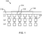
- FIG. 1 is a cross sectional view showing schematically a portion of a typical integrated circuit 110.
- integrated circuit 110 includes multiple layers L1-L3.
- Each layer L1-L3 includes a plurality of copper conductors 112 separated by a dielectric material 114.
- the surface of integrated circuit 110 is covered by capping layer 116.
- Vias 117 connect conductors 112 of one layer to conductors 112 of an adjacent layer.
- Target box 118 shows two dimensions of an area of mixed metal and dielectric to be removed (for example, width and depth). The third dimension of target box 118 (in this case, length) extends into the page and is not shown in FIG. 1 .
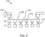
- FIG. 2 is a cross sectional view showing schematically a portion of an integrated circuit following a successful deprocessing event. Only conductors 112 and dielectric 114 within target box 118 were removed during deprocessing (as well as the portion of passivation layer 116 that was within target box 118). No conductors 112 outside of target box 118 were affected by the deprocessing. Milling floor 210 is smooth and uniform, without substantial surface variations in the vertical direction of the cross section, enabling a clear view of the exposed features in layer L2.
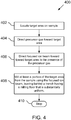
- FIG. 3 is a cross sectional view showing schematically a portion of an integrated circuit following an unsuccessful deprocessing event.
- a portion of conductors 112 outside of target box 118, as well as a portion of dielectric 114 outside of target box 118 was removed during deprocessing.
- milling floor 310 is neither smooth nor uniform.
- the non-uniformity makes visualizing and identifying the structures within the layer more difficult.
- the non-uniformity also increases the difficulty of electrically probing the circuit elements, increasing the likelihood of errors such as probing the wrong element and/or shorting the probe on one of the peaks in the non-uniform milling floor.
- target box 118 is selected to that the layer L1 is milled to expose features of layer L2.
- the non-uniform milling causes a portion of layer L2 to be completely removed (which is supposed to be examined) and a portion of layer L3 to be exposed (which is not supposed to be examined).
- Deprocessing a target area comprising different materials using conventional focused ion beam milling results in non-uniform milling floors and unsuccessful deprocessing events such as the one shown in FIG. 3 .
- the non-uniform milling floor is due to the fact that the different materials are milled at different rates under the influence of the ion beam (i.e., the materials have different sputter rates).
- etch-assisting gases makes the problem worse because known etch-assisting gases enhance the removal of one material in the presence of other materials.
- the selective milling of known etch-assisting gases exacerbates the problem of non-uniform ion beam milling of a target area comprising different materials.
- Using precursor gas that causes different materials in the target area to be milled at the same rate under the influence of the ion beam would result in a more uniform milling floor and more successful deprocessing events, such as the example shown in FIG. 2 .
- Applicants have found that using compounds containing short-chain hydrocarbons and acetate/nitroacetate as a precursor gas causes a focused ion beam to mill copper conductors and low-k dielectrics at substantially similar mill rates.
- the molecular size and carbon content of these compounds is at the threshold of deposition, which slows down the mill rate of the dielectric so that the mill rate of the dielectric is substantially similar to the mill rate of the copper.
- the nitro functional group (NO 2 ) increases the boiling point and reduces the vapor pressure of the compound, making the compound more suitable for use in the vacuum chamber of the ion beam system.
- the precursor gas is selected from a group comprising: methyl acetate, methyl nitroacetate, ethyl acetate, ethyl nitroacetate, propyl acetate, propyl nitroacetate, nitro ethyl acetate, methyl methoxyacetate, or methoxy acetylchloride.
- MNA methyl nitroacetate
- IC integrated circuit
- SiC silicon carbide
- the MNA reduces the selectivity of FIB milling towards copper and dielectric materials, enabling the FIB to mill the different materials at substantially similar mill rates and thereby producing a more uniform milling floor.
- Exemplary low-k dielectric materials include, but are not limited to, carbon-doped silicon dioxide, porous silicon dioxide, and porous carbon-doped silicon dioxide.
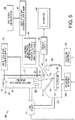
- FIG. 4 is a flowchart 400 showing the steps involved in a preferred embodiment of the present invention which could be used to mill away multiple layers of mixed field materials.
- a target area to be milled is located on the sample.
- the target area will comprise a repair box sufficiently large to expose the appropriate buried active feature for editing.
- the initial target area would preferably be defined as a repair box larger than the final desired repair box.
- the initial target area would preferably be defined as a repair box larger than 20 ⁇ m x 20 ⁇ m.
- the repair box can be reduced by 2-3 ⁇ m to eliminate edge enhancement for the final 20 ⁇ m x 20 ⁇ m repair box.
- the initial repair box could be 30 ⁇ m x 30 ⁇ m.
- the repair box could be reduced by 2-3 ⁇ m so that the final repair box (used when removing the eighth dummy copper layer) could be 20 ⁇ m x 20 ⁇ m.
- the precursor gas is directed toward the target area.
- the gas can be directed at the target area using a gas injection system (GIS).
- GIS gas injection system
- the nozzle of the GIS can precisely direct the flow of the gas in the location of the target area.
- MNA methyl nitroacetate
- methyl acetate, ethyl acetate, ethyl nitroacetate, propyl acetate, propyl nitroacetate, nitro ethyl acetate, methyl methoxyacetate, or methoxy acetylchloride can be used as the precursor gas.
- the focused ion beam is directed toward the target area in the presence of the precursor gas.
- the precursor gas causes the ion beam to mill the dielectric layer more slowly, reducing the mill rate of the dielectric such that the mill rate of the dielectric is substantially similar to the mill rate of the copper.
- the focused ion beam mills at least a portion of the target area from the sample in the presence of the precursor gas, leaving behind a trench having a milling floor that is substantially uniform.
- a typical milling floor is 50 ⁇ m x 50 ⁇ m, but the size can vary as detailed above with respect to multiple layers.
- the method ends at terminator 410.
- FIG. 5 shows a typical focused ion beam system 10 used to implement the present invention.
- Focused ion beam system 10 includes an evacuated envelope 11 having an upper neck portion 12 within which are located a liquid metal ion source 14 and a focusing column 16 including extractor electrodes and an electrostatic optical system.
- Ion beam 18 passes from source 14 through column 16 and between electrostatic deflection means schematically indicated at 20 toward sample 22, which comprises, for example, a semiconductor device positioned on movable X-Y stage 24 within lower chamber 26.
- An ion pump 28 is employed for evacuating neck portion 12.
- the chamber 26 is evacuated with turbomolecular and mechanical pumping system 30 under the control of vacuum controller 32.
- the vacuum system provides within chamber 26 a vacuum of between approximately 1 x 10 -7 Torr and 5 x 10 -4 Torr. When using the precursor gas, the chamber background pressure may rise, typically to about 1 x 10 -5 Torr.
- High voltage power supply 34 is connected to liquid metal ion source 14 as well as to appropriate electrodes in focusing column 16 for forming an approximately 1 keV to 60 keV ion beam 18 and directing the same downwardly.
- Deflection controller and amplifier 36 operated in accordance with a prescribed pattern provided by pattern generator 38, is coupled to deflection plates 20 whereby beam 18 may be controlled to trace out a corresponding pattern on the upper surface of sample 22.
- the deflection plates are placed before the final lens, as is well known in the art.
- the source 14 provides the ions used in the ion beam.
- a plasma ion source such as a Xenon (Xe + ) ion source
- a liquid metal ion source such as a Gallium (Ga + ) ion source
- the source typically is capable of being focused into a sub one-tenth micron wide beam at sample 22 for either modifying the sample 22 by ion milling, enhanced etch, material deposition, or for the purpose of imaging the sample 22.
- a charged particle multiplier 40 used for detecting secondary ion or electron emission for imaging is connected to video circuit and amplifier 42, the latter supplying drive for video monitor 44 also receiving deflection signals from controller 36.
- a charged particle multiplier 40 can be coaxial with the ion beam and include a hole for allowing the ion beam to pass.
- a scanning electron microscope 41, along with its power supply and controls 45, are optionally provided with the FIB system 10.
- a gas delivery system 46 extends into lower chamber 26 for introducing and directing a gaseous vapor toward sample 22.
- Another gas delivery system is described in U.S. Pat. No. 5,435,850 to Rasmussen for a "Gas Injection System,” also assigned to the assignee of the present invention.
- Gas delivery system 46 directs the precursor gas toward the target area.
- a door 60 is opened for inserting sample 22 onto stage 24, which may be heated or cooled, and also for servicing an internal gas supply reservoir, if one is used.
- the door is interlocked so that it cannot be opened if the system is under vacuum.
- the high voltage power supply provides an appropriate acceleration voltage to electrodes in ion beam column 16 for energizing and focusing ion beam 18.
- material is sputtered, that is physically ejected, from the sample. Focused ion beam systems are commercially available, for example, from FEI Company, Hillsboro, Oregon, the assignee of the present application.
- Embodiments of the present invention are directed to a method of removing one or more mixed copper and dielectric layers from an area of a target.
- the method comprises: defining a target area to be removed, the target area including at least a portion of a mixed copper and dielectric layer of a semiconductor device; directing a precursor gas toward the target area; and directing a focused ion beam toward the target area in the presence of the precursor gas, thereby removing at least a portion of a first mixed copper and dielectric layer and producing a uniformly smooth floor in the milled target area; in which the precursor gas causes the focused ion beam to mill the copper at substantially the same rate as the dielectric.
- the method includes a precursor gas selected from a group comprising: methyl acetate, methyl nitroacetate, ethyl acetate, ethyl nitroacetate, propyl acetate, propyl nitroacetate, nitro ethyl acetate, methyl methoxyacetate, and methoxy acetylchloride.
- the method can include removing two or more mixed copper and dielectric layers.
- the two or more mixed copper and dielectric layers can be separated by a layer of dielectric.
- Each mixed copper and dielectric layer can be removed, producing a substantially uniform floor in the milled target area, before the next mixed copper and dielectric layer is milled.
- the method can include a dielectric comprising a low-k dielectric.
- the dielectric is selected from a group comprising: carbon-doped silicon dioxide, porous silicon dioxide, and porous carbon-doped silicon dioxide.
- the method can include milling so that the floor of the milled target area is at least 50 micrometers in length by 50 micrometers in width.
- the method can include a target area that includes a silicon carbide (SiC) capping layer.
- SiC silicon carbide
- inventions of the present invention are directed to a focused ion beam system for removing multiple layers of material.
- the system comprises: an ion source; an ion column including, the ion beam column directing a focused beam of ions from the ion source toward a target area on a semiconductor device, the ion beam column being programmed to direct the focused ion beam to mill away at least a portion of the target area, producing a milling floor having a substantially planar, uniform surface; and a gas injection system for directing a precursor gas toward the target area, the precursor gas causing the focused ion beam to mill, in a mixed layer of copper and dielectric, the copper and the dielectric at substantially the same rate.
- the focused ion beam system can include an ion source that is a plasma ion source.
- the focused ion beam system can include ions in the ion beam which are selected from a group comprising: Xe + , Ga + , Ar + , Kr + , O + , O 2 + , N + , NO + , NO 2 + , Au + , Bi+, Si+, Ge + .
- the focused ion beam system according to the invention includes a precursor gas that is selected from a group comprising: methyl acetate, methyl nitroacetate, ethyl acetate, ethyl nitroacetate, propyl acetate, propyl nitroacetate, nitro ethyl acetate, methyl methoxyacetate, or methoxy acetylchloride.
- the focused ion beam system can include a dielectric comprising a low-k dielectric.
- the dielectric can be selected from a group comprising: carbon-doped silicon dioxide, porous silicon dioxide, and porous carbon-doped silicon dioxide.
- the present invention thus comprises a method of removing one or more mixed copper and dielectric layers from an area of a target as defined by claim 1.
- the method comprises: defining a target area to be removed, the target area including at least a portion of a mixed copper and dielectric layer of a semiconductor device; directing a precursor gas toward the target area; and directing a focused ion beam toward the target area in the presence of the precursor gas; characterized in that at least a portion of a first mixed copper and dielectric layer is removed and a uniformly smooth floor (210) in the milled target area is produced; and the precursor gas causes the focused ion beam to mill the copper at substantially the same rate as the dielectric.
- the method according to the invention includes a precursor gas selected from a group comprising: methyl acetate, methyl nitroacetate, ethyl acetate, ethyl nitroacetate, propyl acetate, propyl nitroacetate, nitro ethyl acetate, methyl methoxyacetate, and methoxy acetylchloride.
- the method can include removing two or more mixed copper and dielectric layers.
- the two or more mixed copper and dielectric layers can be separated by a layer of dielectric.
- Each mixed copper and dielectric layer can be removed, producing a substantially uniform floor in the milled target area, before the next mixed copper and dielectric layer is milled.
- the method can include a dielectric comprising a low-k dielectric.
- the dielectric is selected from a group comprising: carbon-doped silicon dioxide, porous silicon dioxide, and porous carbon-doped silicon dioxide.
- the method can include milling so that the floor of the milled target area is at least 50 micrometers in length by 50 micrometers in width.
- the method can include a target area that includes a silicon carbide (SiC) capping layer.
- SiC silicon carbide
- the invention further provides a focused ion beam system for removing multiple layers of material as defined in claim 9.
- the focused ion beam system can include an ion source that is a plasma ion source.
- the focused ion beam system can include ions in the ion beam which are selected from a group comprising: Xe + , Ga + , Ar + , Kr + , O + , O 2 + , N + , NO + , NO 2 + , Au + , Bi + , Si + , Ge + .
- the focused ion beam system according to the invention comprises a precursor gas that is selected from a group comprising: methyl acetate, methyl nitroacetate, ethyl acetate, ethyl nitroacetate, propyl acetate, propyl nitroacetate, nitro ethyl acetate, methyl methoxyacetate, or methoxy acetylchloride.
- the focused ion beam system can include a dielectric comprising a low-k dielectric.
- the dielectric can be selected from a group comprising: carbon-doped silicon dioxide, porous silicon dioxide, and porous carbon-doped silicon dioxide.
Landscapes
- Engineering & Computer Science (AREA)
- Physics & Mathematics (AREA)
- Chemical & Material Sciences (AREA)
- Power Engineering (AREA)
- Condensed Matter Physics & Semiconductors (AREA)
- General Physics & Mathematics (AREA)
- Manufacturing & Machinery (AREA)
- Computer Hardware Design (AREA)
- Microelectronics & Electronic Packaging (AREA)
- Plasma & Fusion (AREA)
- Analytical Chemistry (AREA)
- Inorganic Chemistry (AREA)
- Chemical Kinetics & Catalysis (AREA)
- General Chemical & Material Sciences (AREA)
- Drying Of Semiconductors (AREA)
- Internal Circuitry In Semiconductor Integrated Circuit Devices (AREA)
Description
- The present invention relates to the field of charged particle beam processing and, in particular, to a method for uniformly removing multiple layers of conductor and dielectric from semiconductor circuits using a focused ion beam.
- Semiconductor devices such as microprocessors can be made up of millions of transistors, each interconnected by thin metallic lines branching over several levels and isolated electrically from each other by layers of dielectric materials. When a new semiconductor design is first produced in a semiconductor fabrication facility, it is typical to find that the design does not operate exactly as expected. It is then necessary for the engineers who designed the device to test their design and "rewire" it to achieve the desired functionality. Due to the complexity of building a semiconductor device in the semiconductor fabrication facility, it typically takes weeks or months to have the redesigned device produced. Further, the changes implemented frequently do not solve the problem or expose a yet further difficulty in the design. The process of testing, re-designing and re-fabrication can significantly lengthen the time to market new semiconductor devices.
- Circuit editing-the process of modifying a circuit during its development without having to remanufacture the whole circuit-provides tremendous economic benefits by reducing both processing costs and development cycle times. In most cases, the feature to be modified is buried under other material, such as insulating layers, and, in the case of "flip chips," semiconductor layers. Therefore it is typically necessary to mill down through these layers of materials to reach the metal feature of interest without damaging adjacent circuit features. This is known as deprocessing. Deprocessing is not limited to circuit editing applications. Deprocessing can be used in other applications where access to buried features located under other material is required. For example, FIB-based Failure Analysis (FA) might require deprocessing to allow access to hidden, lower metal layers for the purpose of fault isolation using passive voltage contrast, or to expose features for electrical probing.
- Over the past decade, techniques have been developed to allow Focused Ion Beam (FIB) systems to reduce the time required for this procedure of perfecting a design. FIB systems produce a narrow, focused beam of charged particles (hereinafter referred to as ions) which is typically scanned across a specimen in a raster fashion, similar to a cathode ray tube. Commercial FIB systems typically use positively charged ions from liquid metal ion sources or plasma ion sources. Modern FIB systems can be used to form an image of a sample surface much like an electron microscope. The intensity at each point of the image is determined by the current of secondary electrons or other particles ejected by the ion beam at the corresponding point on the substrate. The ion beam can also be used to remove material from the sample surface or to deposit material (typically by using a gas that decomposes in the presence of the ion beam and deposits material onto the surface.). When used to remove material, the ions in the focused ion beam physically eject atoms or molecules from the surface by sputtering, that is, by a transfer of momentum from the incoming ions to the atoms at the surface.
- FIB instruments can be used to mill away a target area of a semiconductor device to expose the layers buried within the device. The target area, typically comprising mixed layers of conductor and dielectric, can be milled by rastering a beam of ions across the area of interest. The beam is typically scanned across the area to be milled using digital electronics that step the beam from point to point. The distance between points is referred to as the pixel spacing. Pixel spacing is typically less than the beam spot size, that is, each subsequent beam position overlaps the previous position in an attempt to obtain a uniform cut and a smooth finish. This method is referred to as 'Default Milling'. Milling methods have been well documented, for example, in
U.S. Pat. No. 5,188,705 to Swanson , et. al. for "Method of Semiconductor Device Manufacture". - During FIB processing for circuit editing or failure analysis (FA), it is common to have to deprocess a relatively large area of multiple layers, each layer having copper and dielectric materials embedded in the same layer. When these types of mixed layers are sputtered by a FIB, the difference in sputtering rate between copper and the dielectric material also tends to result in a non-uniform milling floor.
- Chemistries have been developed that selectively attack certain materials, causing it to sputter more quickly in the presence of certain gases than with just the ion beam alone. This process is well-known within the art and is commonly referred to as Gas Assisted Etching (GAE). Because it speeds up the removal process, GAE can be used, for example, to mill relatively large areas of a surface layer or layers to expose underlying layers for observation and testing. However, one drawback with using GAE to mill relatively large areas of a surface layer comprising mixed materials is that the chemistries used to assist FIB milling typically enhance the removal of one material in the presence of other materials. One material is selectively etched at a higher rate than the other, exacerbating the problem of a non-uniform milling floor. For example,
U.S. Patent No. 7,883,630 relates to chemistries for copper removal but emphasizes the selective removal of copper relative to dielectrics, rather than the 1:1 removal rates that are ideal for planar deprocessing. Water can be used for planar deprocessing on semiconductor devices with Si3N4 etch stops, but it is not effective on modern devices with SiC capping layers. - Although several techniques to improve the uniformity of copper milling are known, none of these techniques adequately solve the problems of milling through mixed copper and dielectric layers. Hence, there is a need for an improved technique to allow more uniform milling through multiple layers of mixed copper and dielectric for planar deprocessing with a focused ion beam.
- To aid in understanding embodiments of the invention, the following documents may serve as useful background information.
EP1465243 discloses a method for uniformly removing multiple layers of conductor and dielectric, such as the removal of multiple layers consisting of dummy copper pads and SiO2 on a semiconductor device. Variable Pixel Milling is first used to more uniformly remove most of a layer of conductor and dielectric. Focused ion beam sputtering in conjunction with an oxygen containing gas, such as H2O vapor or oxygen, is then used to smooth out the trench floor before the next layer is removed. Pat. App. Pub.20050072756 - An object of the invention, therefore, is to provide a method for more uniformly removing multiple layers of conductor and dielectric-such as the removal of multiple layers consisting of copper and a low k dielectric-in a manner allowing access to active features buried underneath these layers for applications including, but not limited to, circuit editing and failure analysis. An embodiment of the present invention is directed to a method of removing one or more mixed copper and dielectric layers from an area of a target. The method comprises defining a target area to be removed, the target area including at least a portion of a mixed copper and dielectric layer of a semiconductor device; directing a precursor gas toward the target area; and directing a focused ion beam toward the target area in the presence of the precursor gas, thereby removing at least a portion of a first mixed copper and dielectric layer and producing a uniformly smooth floor in the milled target area. The precursor gas causes the focused ion beam to mill the copper at substantially the same rate as the dielectric. According to the invention the precursor gas is selected from a group comprising: methyl acetate, methyl nitroacetate, ethyl acetate, ethyl nitroacetate, propyl acetate, propyl nitroacetate, nitro ethyl acetate, methyl methoxyacetate, or methoxy acetylchloride. In a preferred embodiment, the precursor gas comprises methyl nitroacetate.
- Another embodiment of the present invention is directed to a focused ion beam system for removing multiple layers of material. The system comprises an ion source; an ion beam focusing column for directing a focused ion beam from the ion source toward a target area on a semiconductor device, the ion beam focusing column being programmed to direct the focused ion beam to mill away at least a portion of the target area to produce a milling floor having a substantially planar, uniform surface; a precursor gas; and a gas injection system for directing the precursor gas toward the target area. The ion beam, when used to mill the target area of the semiconductor device that includes a mixed layer of copper and dielectric in the presence of the precursor gas, causes the copper to be milled at substantially the same rate as the dielectric, thereby producing a milling floor having a substantially planar, uniform surface. According to the invention the precursor gas is selected from a group comprising: methyl acetate, methyl nitroacetate, ethyl acetate, ethyl nitroacetate, propyl acetate, propyl nitroacetate, nitro ethyl acetate, methyl methoxyacetate, or methoxy acetylchloride. In a preferred embodiment, the precursor gas comprises methyl nitroacetate.
- The foregoing has outlined rather broadly the features and technical advantages of the present invention in order that the detailed description of the invention that follows may be better understood. Additional features and advantages of the invention will be described hereinafter.
- For a more complete understanding of the present invention, and the advantages thereof, reference is now made to the following descriptions taken in conjunction with the accompanying drawings, in which:
-
FIG. 1 is a cross sectional view showing schematically a portion of a typicalintegrated circuit 110; -
FIG. 2 is a cross sectional view showing schematically a portion of an integrated circuit following a successful deprocessing event; -
FIG. 3 is a cross sectional view showing schematically a portion of an integrated circuit following an unsuccessful deprocessing event; -
FIG. 4 is a flowchart showing the steps of a preferred embodiment of the present invention; -
FIG. 5 shows schematically a typical focused ion beam system used in a preferred embodiment of the invention; - A preferred embodiment of this invention provides a method for uniformly removing multiple layers of mixed conductor and dielectric-such as the removal of multiple layers consisting of copper and low k dielectric-in a manner allowing access to the active features buried underneath these layers for applications including, but not limited to, circuit editing and failure analysis.
- Preferred embodiments of the present invention are directed to a method used for milling of materials, particularly copper-based features within semiconductor devices. Although much of the following description is directed toward copper milling and specifically copper milling within semiconductor devices, the apparatus and methods of the present invention could equally be utilized in the milling of other materials. The techniques described herein can be used by themselves or in combination with other techniques. Hence, the scope of the present invention should not be limited to simply the milling of copper-based structures.
-
FIG. 1 is a cross sectional view showing schematically a portion of a typicalintegrated circuit 110. As shown inFIG. 1 , integratedcircuit 110 includes multiple layers L1-L3. Each layer L1-L3 includes a plurality ofcopper conductors 112 separated by adielectric material 114. The surface ofintegrated circuit 110 is covered by cappinglayer 116.Vias 117 connectconductors 112 of one layer toconductors 112 of an adjacent layer.Target box 118 shows two dimensions of an area of mixed metal and dielectric to be removed (for example, width and depth). The third dimension of target box 118 (in this case, length) extends into the page and is not shown inFIG. 1 . -
FIG. 2 is a cross sectional view showing schematically a portion of an integrated circuit following a successful deprocessing event.Only conductors 112 and dielectric 114 withintarget box 118 were removed during deprocessing (as well as the portion ofpassivation layer 116 that was within target box 118). Noconductors 112 outside oftarget box 118 were affected by the deprocessing. Millingfloor 210 is smooth and uniform, without substantial surface variations in the vertical direction of the cross section, enabling a clear view of the exposed features in layer L2. -
FIG. 3 is a cross sectional view showing schematically a portion of an integrated circuit following an unsuccessful deprocessing event. A portion ofconductors 112 outside oftarget box 118, as well as a portion ofdielectric 114 outside oftarget box 118 was removed during deprocessing. In addition, millingfloor 310 is neither smooth nor uniform. The non-uniformity makes visualizing and identifying the structures within the layer more difficult. The non-uniformity also increases the difficulty of electrically probing the circuit elements, increasing the likelihood of errors such as probing the wrong element and/or shorting the probe on one of the peaks in the non-uniform milling floor. Additionally,target box 118 is selected to that the layer L1 is milled to expose features of layer L2. In an unsuccessful deprocessing event such as the one shown inFIG. 3 , the non-uniform milling causes a portion of layer L2 to be completely removed (which is supposed to be examined) and a portion of layer L3 to be exposed (which is not supposed to be examined). - Deprocessing a target area comprising different materials using conventional focused ion beam milling results in non-uniform milling floors and unsuccessful deprocessing events such as the one shown in
FIG. 3 . The non-uniform milling floor is due to the fact that the different materials are milled at different rates under the influence of the ion beam (i.e., the materials have different sputter rates). Using known etch-assisting gases makes the problem worse because known etch-assisting gases enhance the removal of one material in the presence of other materials. The selective milling of known etch-assisting gases exacerbates the problem of non-uniform ion beam milling of a target area comprising different materials. - Using precursor gas that causes different materials in the target area to be milled at the same rate under the influence of the ion beam would result in a more uniform milling floor and more successful deprocessing events, such as the example shown in
FIG. 2 . For target areas comprising a mixed layer of copper conductors and low-k dielectric, Applicants have found that using compounds containing short-chain hydrocarbons and acetate/nitroacetate as a precursor gas causes a focused ion beam to mill copper conductors and low-k dielectrics at substantially similar mill rates. The molecular size and carbon content of these compounds is at the threshold of deposition, which slows down the mill rate of the dielectric so that the mill rate of the dielectric is substantially similar to the mill rate of the copper. The nitro functional group (NO2) increases the boiling point and reduces the vapor pressure of the compound, making the compound more suitable for use in the vacuum chamber of the ion beam system. - According to the invention the precursor gas is selected from a group comprising: methyl acetate, methyl nitroacetate, ethyl acetate, ethyl nitroacetate, propyl acetate, propyl nitroacetate, nitro ethyl acetate, methyl methoxyacetate, or methoxy acetylchloride. In preferred embodiments of the present invention, methyl nitroacetate (MNA) is used as a precursor gas for the removal of "mixed field materials" on integrated circuit (IC) devices comprising copper in porous, ultra low-k dielectric materials with silicon carbide (SiC) capping layers. The MNA reduces the selectivity of FIB milling towards copper and dielectric materials, enabling the FIB to mill the different materials at substantially similar mill rates and thereby producing a more uniform milling floor. Exemplary low-k dielectric materials include, but are not limited to, carbon-doped silicon dioxide, porous silicon dioxide, and porous carbon-doped silicon dioxide.
-
FIG. 4 is aflowchart 400 showing the steps involved in a preferred embodiment of the present invention which could be used to mill away multiple layers of mixed field materials. Instep 402, a target area to be milled is located on the sample. Typically, where one or more layers of copper and dielectric must be removed from a semiconductor device to allow circuit editing or failure analysis activities, the target area will comprise a repair box sufficiently large to expose the appropriate buried active feature for editing. Further, where more than two layers of copper and dielectric must be removed, the initial target area would preferably be defined as a repair box larger than the final desired repair box. If, for example, a 20□m x 20□m repair box is required for the final layer, the initial target area would preferably be defined as a repair box larger than 20□m x 20□m. In order to compensate for undesirable over-etching that occurs at the edges of a repair box, for every two layers to be removed, the repair box can be reduced by 2-3□□m to eliminate edge enhancement for the final 20□m x 20□m repair box. To illustrate, if eight layers are to be removed, the initial repair box could be 30□m x 30□m. For every two layers removed, the repair box could be reduced by 2-3□□m so that the final repair box (used when removing the eighth dummy copper layer) could be 20□m x 20□m. - In
step 404, the precursor gas is directed toward the target area. The gas can be directed at the target area using a gas injection system (GIS). The nozzle of the GIS can precisely direct the flow of the gas in the location of the target area. As mentioned above, in preferred embodiments of the present invention, methyl nitroacetate (MNA) is used as the precursor gas. In alternative embodiments, methyl acetate, ethyl acetate, ethyl nitroacetate, propyl acetate, propyl nitroacetate, nitro ethyl acetate, methyl methoxyacetate, or methoxy acetylchloride can be used as the precursor gas. Instep 406, the focused ion beam is directed toward the target area in the presence of the precursor gas. The precursor gas causes the ion beam to mill the dielectric layer more slowly, reducing the mill rate of the dielectric such that the mill rate of the dielectric is substantially similar to the mill rate of the copper. Instep 408, the focused ion beam mills at least a portion of the target area from the sample in the presence of the precursor gas, leaving behind a trench having a milling floor that is substantially uniform. A typical milling floor is 50□m x 50□m, but the size can vary as detailed above with respect to multiple layers. The method ends atterminator 410. -
FIG. 5 shows a typical focusedion beam system 10 used to implement the present invention. Focusedion beam system 10 includes an evacuatedenvelope 11 having anupper neck portion 12 within which are located a liquidmetal ion source 14 and a focusingcolumn 16 including extractor electrodes and an electrostatic optical system.Ion beam 18 passes fromsource 14 throughcolumn 16 and between electrostatic deflection means schematically indicated at 20 towardsample 22, which comprises, for example, a semiconductor device positioned on movableX-Y stage 24 withinlower chamber 26. An ion pump 28 is employed for evacuatingneck portion 12. Thechamber 26 is evacuated with turbomolecular andmechanical pumping system 30 under the control ofvacuum controller 32. The vacuum system provides within chamber 26 a vacuum of between approximately 1 x 10⁻⁷ Torr and 5 x 10⁻⁴ Torr. When using the precursor gas, the chamber background pressure may rise, typically to about 1 x 10⁻⁵ Torr. - High
voltage power supply 34 is connected to liquidmetal ion source 14 as well as to appropriate electrodes in focusingcolumn 16 for forming an approximately 1 keV to 60keV ion beam 18 and directing the same downwardly. Deflection controller andamplifier 36, operated in accordance with a prescribed pattern provided bypattern generator 38, is coupled todeflection plates 20 wherebybeam 18 may be controlled to trace out a corresponding pattern on the upper surface ofsample 22. In some systems the deflection plates are placed before the final lens, as is well known in the art. - The
source 14 provides the ions used in the ion beam. In preferred embodiments of the present invention, a plasma ion source, such as a Xenon (Xe+) ion source, is used. In alternative embodiments, a liquid metal ion source, such as a Gallium (Ga+) ion source, is used. The source typically is capable of being focused into a sub one-tenth micron wide beam atsample 22 for either modifying thesample 22 by ion milling, enhanced etch, material deposition, or for the purpose of imaging thesample 22. A chargedparticle multiplier 40 used for detecting secondary ion or electron emission for imaging is connected to video circuit andamplifier 42, the latter supplying drive for video monitor 44 also receiving deflection signals fromcontroller 36. The location of chargedparticle multiplier 40 withinchamber 26 can vary in different embodiments. For example, a chargedparticle multiplier 40 can be coaxial with the ion beam and include a hole for allowing the ion beam to pass. Ascanning electron microscope 41, along with its power supply and controls 45, are optionally provided with theFIB system 10. - A
gas delivery system 46 extends intolower chamber 26 for introducing and directing a gaseous vapor towardsample 22.U.S. Pat. No. 5,851,413 to Casella et al. for "Gas Delivery Systems For Particle Beam Processing," assigned to the assignee of the present invention, describes a suitablefluid delivery system 46. Another gas delivery system is described inU.S. Pat. No. 5,435,850 to Rasmussen for a "Gas Injection System," also assigned to the assignee of the present invention.Gas delivery system 46 directs the precursor gas toward the target area. - A
door 60 is opened for insertingsample 22 ontostage 24, which may be heated or cooled, and also for servicing an internal gas supply reservoir, if one is used. The door is interlocked so that it cannot be opened if the system is under vacuum. The high voltage power supply provides an appropriate acceleration voltage to electrodes inion beam column 16 for energizing and focusingion beam 18. When it strikessample 22, material is sputtered, that is physically ejected, from the sample. Focused ion beam systems are commercially available, for example, from FEI Company, Hillsboro, Oregon, the assignee of the present application. - Embodiments of the present invention are directed to a method of removing one or more mixed copper and dielectric layers from an area of a target. The method comprises: defining a target area to be removed, the target area including at least a portion of a mixed copper and dielectric layer of a semiconductor device; directing a precursor gas toward the target area; and directing a focused ion beam toward the target area in the presence of the precursor gas, thereby removing at least a portion of a first mixed copper and dielectric layer and producing a uniformly smooth floor in the milled target area; in which the precursor gas causes the focused ion beam to mill the copper at substantially the same rate as the dielectric.
- The method includes a precursor gas selected from a group comprising: methyl acetate, methyl nitroacetate, ethyl acetate, ethyl nitroacetate, propyl acetate, propyl nitroacetate, nitro ethyl acetate, methyl methoxyacetate, and methoxy acetylchloride.
- The method can include removing two or more mixed copper and dielectric layers. The two or more mixed copper and dielectric layers can be separated by a layer of dielectric. Each mixed copper and dielectric layer can be removed, producing a substantially uniform floor in the milled target area, before the next mixed copper and dielectric layer is milled.
- The method can include a dielectric comprising a low-k dielectric. The dielectric is selected from a group comprising: carbon-doped silicon dioxide, porous silicon dioxide, and porous carbon-doped silicon dioxide.
- The method can include milling so that the floor of the milled target area is at least 50 micrometers in length by 50 micrometers in width.
- The method can include a target area that includes a silicon carbide (SiC) capping layer.
- Other embodiments of the present invention are directed to a focused ion beam system for removing multiple layers of material. The system comprises: an ion source; an ion column including, the ion beam column directing a focused beam of ions from the ion source toward a target area on a semiconductor device, the ion beam column being programmed to direct the focused ion beam to mill away at least a portion of the target area, producing a milling floor having a substantially planar, uniform surface; and a gas injection system for directing a precursor gas toward the target area, the precursor gas causing the focused ion beam to mill, in a mixed layer of copper and dielectric, the copper and the dielectric at substantially the same rate.
- The focused ion beam system can include an ion source that is a plasma ion source.
- The focused ion beam system can include ions in the ion beam which are selected from a group comprising: Xe+, Ga+, Ar+, Kr+, O+, O2 +, N+, NO+, NO2 +, Au+, Bi+, Si+, Ge+. The focused ion beam system according to the invention includes a precursor gas that is selected from a group comprising: methyl acetate, methyl nitroacetate, ethyl acetate, ethyl nitroacetate, propyl acetate, propyl nitroacetate, nitro ethyl acetate, methyl methoxyacetate, or methoxy acetylchloride.
- The focused ion beam system can include a dielectric comprising a low-k dielectric. The dielectric can be selected from a group comprising: carbon-doped silicon dioxide, porous silicon dioxide, and porous carbon-doped silicon dioxide.
- The present invention thus comprises a method of removing one or more mixed copper and dielectric layers from an area of a target as defined by claim 1. The method comprises: defining a target area to be removed, the target area including at least a portion of a mixed copper and dielectric layer of a semiconductor device; directing a precursor gas toward the target area; and directing a focused ion beam toward the target area in the presence of the precursor gas; characterized in that at least a portion of a first mixed copper and dielectric layer is removed and a uniformly smooth floor (210) in the milled target area is produced; and the precursor gas causes the focused ion beam to mill the copper at substantially the same rate as the dielectric.
- The method according to the invention includes a precursor gas selected from a group comprising: methyl acetate, methyl nitroacetate, ethyl acetate, ethyl nitroacetate, propyl acetate, propyl nitroacetate, nitro ethyl acetate, methyl methoxyacetate, and methoxy acetylchloride.
- The method can include removing two or more mixed copper and dielectric layers. The two or more mixed copper and dielectric layers can be separated by a layer of dielectric. Each mixed copper and dielectric layer can be removed, producing a substantially uniform floor in the milled target area, before the next mixed copper and dielectric layer is milled.
- The method can include a dielectric comprising a low-k dielectric. The dielectric is selected from a group comprising: carbon-doped silicon dioxide, porous silicon dioxide, and porous carbon-doped silicon dioxide.
- The method can include milling so that the floor of the milled target area is at least 50 micrometers in length by 50 micrometers in width.
- The method can include a target area that includes a silicon carbide (SiC) capping layer.
- The invention further provides a focused ion beam system for removing multiple layers of material as defined in claim 9.
- The focused ion beam system can include an ion source that is a plasma ion source.
- The focused ion beam system can include ions in the ion beam which are selected from a group comprising: Xe+, Ga+, Ar+, Kr+, O+, O2 +, N+, NO+, NO2 +, Au+, Bi+, Si+, Ge+. The focused ion beam system according to the invention comprises a precursor gas that is selected from a group comprising: methyl acetate, methyl nitroacetate, ethyl acetate, ethyl nitroacetate, propyl acetate, propyl nitroacetate, nitro ethyl acetate, methyl methoxyacetate, or methoxy acetylchloride.
- The focused ion beam system can include a dielectric comprising a low-k dielectric. The dielectric can be selected from a group comprising: carbon-doped silicon dioxide, porous silicon dioxide, and porous carbon-doped silicon dioxide.
- Although the present invention and its advantages have been described in detail, it should be understood that various changes, substitutions and alterations can be made to the embodiments described herein without departing from the scope of the invention as defined by the appended claims. Moreover, the scope of the present application is not intended to be limited to the particular embodiments of the process, machine, manufacture, composition of matter, means, methods and steps described in the specification.
Claims (13)
- A method of removing one or more mixed copper and dielectric layers from an area of a target, the method comprising:defining a target area (118) to be removed, the target area including at least a portion of a mixed copper and dielectric layer of a semiconductor device;directing a precursor gas toward the target area; anddirecting a focused ion beam (18) toward the target area in the presence of the precursor gas;characterized in that at least a portion of a first mixed copper and dielectric layer is removed and a uniformly smooth floor (210) in the milled target area is produced;in which the precursor gas is selected from a group comprising: methyl acetate, methyl nitroacetate, ethyl acetate, ethyl nitroacetate, propyl acetate, propyl nitroacetate, nitro ethyl acetate, methyl methoxyacetate, and methoxy acetylchloride; andthe precursor gas causes the focused ion beam to mill the copper at substantially the same rate as the dielectric.
- The method of claim 1 in which two or more mixed copper and dielectric layers are removed.
- The method of claim 2 in which said two or more mixed copper and dielectric layers are separated by a layer of dielectric.
- The method of claim 2 in which each mixed copper and dielectric layer is removed producing a substantially uniform floor (210) in the milled target area before the next mixed copper and dielectric layer is milled.
- The method of claim 1 in which the dielectric comprises a low-k dielectric.
- The method of claim 1 in which the dielectric is selected from a group comprising: carbon-doped silicon dioxide, porous silicon dioxide, and porous carbon-doped silicon dioxide.
- The method of claim 1 in which the floor of the milled target area is at least 50 micrometers in length by 50 micrometers in width.
- The method of claim 1 in which the target area includes a silicon carbide (SiC) capping layer.
- A focused ion beam system for removing multiple layers of material, the system comprising:an ion source (14);an ion beam focusing column (16) for directing a focused ion beam (18) from the ion source toward a target area (118) on a semiconductor device (22), the ion beam focusing column being programmed to direct the focused ion beam to mill away at least a portion of the target area;a precursor gas; anda gas injection system (46) for directing the precursor gas toward the target area;characterized in that:the ion beam (18), when used to mill the target area (118) of the semiconductor device (22) that includes a mixed layer of copper and dielectric in the presence of the precursor gas, causes the copper to be milled at substantially the same rate as the dielectric, thereby producing a milling floor (210) having a substantially planar, uniform surface,the precursor gas being selected from a group comprising: methyl acetate, methyl nitroacetate, ethyl acetate, ethyl nitroacetate, propyl acetate, propyl nitroacetate, nitro ethyl acetate, methyl methoxyacetate, and methoxy acetylchloride.
- The focused ion beam system of claim 9, in which the ion source is a plasma ion source.
- The focused ion beam system of claim 9 or claim 10, in which the ions in the ion beam are selected from a group comprising: Xe+, Ga+, Ar+, Kr+, O+, O2 +, N+, NO+, NO2 +, Au+, Bi+, Si+, Ge+.
- The focused ion beam system of claim 9 or claim 10, in which the dielectric comprises a low-k dielectric.
- The focused ion beam system of claim 9 or claim 10, in which the dielectric is selected from a group comprising: carbon-doped silicon dioxide, porous silicon dioxide, and porous carbon-doped silicon dioxide.
Applications Claiming Priority (2)
| Application Number | Priority Date | Filing Date | Title |
|---|---|---|---|
| US201361828128P | 2013-05-28 | 2013-05-28 | |
| US13/910,761 US9064811B2 (en) | 2013-05-28 | 2013-06-05 | Precursor for planar deprocessing of semiconductor devices using a focused ion beam |
Publications (2)
| Publication Number | Publication Date |
|---|---|
| EP2808885A1 EP2808885A1 (en) | 2014-12-03 |
| EP2808885B1 true EP2808885B1 (en) | 2018-09-12 |
Family
ID=50774752
Family Applications (1)
| Application Number | Title | Priority Date | Filing Date |
|---|---|---|---|
| EP14169930.6A Active EP2808885B1 (en) | 2013-05-28 | 2014-05-27 | Precursor for planar deprocessing of semiconductor devices using a focused ion beam |
Country Status (4)
| Country | Link |
|---|---|
| US (2) | US9064811B2 (en) |
| EP (1) | EP2808885B1 (en) |
| JP (1) | JP6393446B2 (en) |
| CN (1) | CN104217912B (en) |
Families Citing this family (15)
| Publication number | Priority date | Publication date | Assignee | Title |
|---|---|---|---|---|
| US9123506B2 (en) | 2013-06-10 | 2015-09-01 | Fei Company | Electron beam-induced etching |
| US9978586B2 (en) | 2015-11-06 | 2018-05-22 | Fei Company | Method of material deposition |
| US10103008B2 (en) * | 2016-01-12 | 2018-10-16 | Fei Company | Charged particle beam-induced etching |
| US10347463B2 (en) * | 2016-12-09 | 2019-07-09 | Fei Company | Enhanced charged particle beam processes for carbon removal |
| EP3607578B1 (en) * | 2017-04-04 | 2023-07-19 | TESCAN Brno, s.r.o. | A method of etching one or more of mixed metal and dielectric layer of a semiconductor device |
| US10546719B2 (en) * | 2017-06-02 | 2020-01-28 | Fei Company | Face-on, gas-assisted etching for plan-view lamellae preparation |
| CZ310048B6 (en) * | 2017-07-25 | 2024-06-19 | Tescan Group, A.S. | A method of material removal |
| FR3079963A1 (en) * | 2018-04-04 | 2019-10-11 | Tescan Brno, S.R.O. | METHOD FOR ETCHING ONE OR MORE MIXED METAL AND DIELECTRIC LAYERS OF A SEMICONDUCTOR DEVICE |
| ES2738911A1 (en) * | 2018-07-25 | 2020-01-27 | Consejo Superior Investigacion | PROCEDURE FOR DEPOSITING ELEMENTS ON A SUBSTRATE OF INTEREST AND DEVICE (Machine-translation by Google Translate, not legally binding) |
| US10811219B2 (en) | 2018-08-07 | 2020-10-20 | Applied Materials Israel Ltd. | Method for evaluating a region of an object |
| CN109148315B (en) * | 2018-08-27 | 2020-11-10 | 苏州芯联成软件有限公司 | Method for distinguishing through hole connection between two metal layers in chip |
| EP3884264A4 (en) * | 2018-11-21 | 2022-08-03 | Techinsights Inc. | Ion beam delayering system and method, topographically enhanced delayered sample produced thereby, and imaging methods and systems related thereto |
| KR102613856B1 (en) * | 2019-06-21 | 2023-12-14 | 에프이아이 컴파니 | Perimeter trench formation and delineation etch delayering |
| US11636997B2 (en) | 2020-07-01 | 2023-04-25 | Applied Materials Israel Ltd. | Uniform milling of adjacent materials using parallel scanning fib |
| CZ202363A3 (en) | 2023-02-19 | 2024-10-09 | Tescan Group, A.S. | An equipment with focused beam of charged particles and a method of processing or displaying samples |
Citations (2)
| Publication number | Priority date | Publication date | Assignee | Title |
|---|---|---|---|---|
| US6083840A (en) * | 1998-11-25 | 2000-07-04 | Arch Specialty Chemicals, Inc. | Slurry compositions and method for the chemical-mechanical polishing of copper and copper alloys |
| US20080257862A1 (en) * | 2005-01-25 | 2008-10-23 | Irina Belov | Method of chemical mechanical polishing of a copper structure using a slurry having a multifunctional activator |
Family Cites Families (17)
| Publication number | Priority date | Publication date | Assignee | Title |
|---|---|---|---|---|
| US5188705A (en) | 1991-04-15 | 1993-02-23 | Fei Company | Method of semiconductor device manufacture |
| US5435850A (en) | 1993-09-17 | 1995-07-25 | Fei Company | Gas injection system |
| US5851413A (en) | 1996-06-19 | 1998-12-22 | Micrion Corporation | Gas delivery systems for particle beam processing |
| US6268608B1 (en) | 1998-10-09 | 2001-07-31 | Fei Company | Method and apparatus for selective in-situ etching of inter dielectric layers |
| US6514866B2 (en) * | 2001-01-12 | 2003-02-04 | North Carolina State University | Chemically enhanced focused ion beam micro-machining of copper |
| US6824655B2 (en) * | 2001-08-27 | 2004-11-30 | Credence Systems Corporation | Process for charged particle beam micro-machining of copper |
| US7008803B2 (en) * | 2002-10-24 | 2006-03-07 | International Business Machines Corporation | Method of reworking structures incorporating low-k dielectric materials |
| US6863787B2 (en) | 2003-04-02 | 2005-03-08 | Fei Company | Dummy copper deprocessing |
| US7060196B2 (en) | 2003-10-03 | 2006-06-13 | Credence Systems Corporation | FIB milling of copper over organic dielectrics |
| US7670956B2 (en) | 2005-04-08 | 2010-03-02 | Fei Company | Beam-induced etching |
| US20080113455A1 (en) * | 2006-11-11 | 2008-05-15 | Rajesh Jain | Planar etching of dissimilar materials |
| JP2009043973A (en) * | 2007-08-09 | 2009-02-26 | Tokyo Electron Ltd | Manufacturing method of semiconductor device, treatment device of semiconductor substrate, and storage medium |
| US8778804B2 (en) | 2009-01-30 | 2014-07-15 | Fei Company | High selectivity, low damage electron-beam delineation etch |
| US20110048931A1 (en) * | 2009-08-25 | 2011-03-03 | Makarov Vladimir V | FIB Process for Selective and Clean Etching of Copper |
| KR101967853B1 (en) * | 2011-09-12 | 2019-04-10 | 에프이아이 컴파니 | Glancing angle mill |
| CA2791249C (en) * | 2011-11-10 | 2014-02-25 | Semiconductor Insights Inc. | Method and system for ion beam delayering of a sample and control thereof |
| US9443697B2 (en) | 2012-01-31 | 2016-09-13 | Fei Company | Low energy ion beam etch |
-
2013
- 2013-06-05 US US13/910,761 patent/US9064811B2/en active Active
-
2014
- 2014-05-26 JP JP2014107733A patent/JP6393446B2/en active Active
- 2014-05-27 CN CN201410227896.7A patent/CN104217912B/en active Active
- 2014-05-27 EP EP14169930.6A patent/EP2808885B1/en active Active
-
2015
- 2015-06-23 US US14/747,491 patent/US9761467B2/en active Active
Patent Citations (2)
| Publication number | Priority date | Publication date | Assignee | Title |
|---|---|---|---|---|
| US6083840A (en) * | 1998-11-25 | 2000-07-04 | Arch Specialty Chemicals, Inc. | Slurry compositions and method for the chemical-mechanical polishing of copper and copper alloys |
| US20080257862A1 (en) * | 2005-01-25 | 2008-10-23 | Irina Belov | Method of chemical mechanical polishing of a copper structure using a slurry having a multifunctional activator |
Also Published As
| Publication number | Publication date |
|---|---|
| US20140357088A1 (en) | 2014-12-04 |
| US9064811B2 (en) | 2015-06-23 |
| US9761467B2 (en) | 2017-09-12 |
| JP2014232876A (en) | 2014-12-11 |
| CN104217912A (en) | 2014-12-17 |
| US20150294885A1 (en) | 2015-10-15 |
| JP6393446B2 (en) | 2018-09-19 |
| CN104217912B (en) | 2018-02-06 |
| EP2808885A1 (en) | 2014-12-03 |
Similar Documents
| Publication | Publication Date | Title |
|---|---|---|
| EP2808885B1 (en) | Precursor for planar deprocessing of semiconductor devices using a focused ion beam | |
| US10529538B2 (en) | Endpointing for focused ion beam processing | |
| US6322672B1 (en) | Method and apparatus for milling copper interconnects in a charged particle beam system | |
| KR102273042B1 (en) | Face-on, gas-assisted etching for plan-view lamellae preparation | |
| US8778804B2 (en) | High selectivity, low damage electron-beam delineation etch | |
| US7858936B2 (en) | Slice and view with decoration | |
| US9443697B2 (en) | Low energy ion beam etch | |
| US20060219949A1 (en) | Fib milling of copper over organic dielectrics | |
| US6863787B2 (en) | Dummy copper deprocessing | |
| Xia et al. | Enhancement of XeF2-assisted gallium ion beam etching of silicon layer and endpoint detection from backside in circuit editing | |
| EP1048071A1 (en) | Integrated circuit rewiring using gas-assisted fib etching | |
| US10347463B2 (en) | Enhanced charged particle beam processes for carbon removal | |
| US20040132287A1 (en) | Dry etch process for copper | |
| Wang et al. | Focused ion beam analysis technology | |
| JP2007142453A (en) | Cross section observation method and cross section observation device of semiconductor device | |
| KR20060076893A (en) | Method for reducing the charge-up ion of focused ion beam apparatu |
Legal Events
| Date | Code | Title | Description |
|---|---|---|---|
| PUAI | Public reference made under article 153(3) epc to a published international application that has entered the european phase |
Free format text: ORIGINAL CODE: 0009012 |
|
| 17P | Request for examination filed |
Effective date: 20140527 |
|
| AK | Designated contracting states |
Kind code of ref document: A1 Designated state(s): AL AT BE BG CH CY CZ DE DK EE ES FI FR GB GR HR HU IE IS IT LI LT LU LV MC MK MT NL NO PL PT RO RS SE SI SK SM TR |
|
| AX | Request for extension of the european patent |
Extension state: BA ME |
|
| R17P | Request for examination filed (corrected) |
Effective date: 20150528 |
|
| RBV | Designated contracting states (corrected) |
Designated state(s): AL AT BE BG CH CY CZ DE DK EE ES FI FR GB GR HR HU IE IS IT LI LT LU LV MC MK MT NL NO PL PT RO RS SE SI SK SM TR |
|
| STAA | Information on the status of an ep patent application or granted ep patent |
Free format text: STATUS: EXAMINATION IS IN PROGRESS |
|
| 17Q | First examination report despatched |
Effective date: 20170713 |
|
| GRAP | Despatch of communication of intention to grant a patent |
Free format text: ORIGINAL CODE: EPIDOSNIGR1 |
|
| STAA | Information on the status of an ep patent application or granted ep patent |
Free format text: STATUS: GRANT OF PATENT IS INTENDED |
|
| GRAJ | Information related to disapproval of communication of intention to grant by the applicant or resumption of examination proceedings by the epo deleted |
Free format text: ORIGINAL CODE: EPIDOSDIGR1 |
|
| STAA | Information on the status of an ep patent application or granted ep patent |
Free format text: STATUS: EXAMINATION IS IN PROGRESS |
|
| INTG | Intention to grant announced |
Effective date: 20180507 |
|
| GRAP | Despatch of communication of intention to grant a patent |
Free format text: ORIGINAL CODE: EPIDOSNIGR1 |
|
| STAA | Information on the status of an ep patent application or granted ep patent |
Free format text: STATUS: GRANT OF PATENT IS INTENDED |
|
| INTC | Intention to grant announced (deleted) | ||
| INTG | Intention to grant announced |
Effective date: 20180613 |
|
| GRAS | Grant fee paid |
Free format text: ORIGINAL CODE: EPIDOSNIGR3 |
|
| GRAA | (expected) grant |
Free format text: ORIGINAL CODE: 0009210 |
|
| STAA | Information on the status of an ep patent application or granted ep patent |
Free format text: STATUS: THE PATENT HAS BEEN GRANTED |
|
| AK | Designated contracting states |
Kind code of ref document: B1 Designated state(s): AL AT BE BG CH CY CZ DE DK EE ES FI FR GB GR HR HU IE IS IT LI LT LU LV MC MK MT NL NO PL PT RO RS SE SI SK SM TR |
|
| REG | Reference to a national code |
Ref country code: GB Ref legal event code: FG4D |
|
| REG | Reference to a national code |
Ref country code: CH Ref legal event code: EP |
|
| REG | Reference to a national code |
Ref country code: IE Ref legal event code: FG4D |
|
| REG | Reference to a national code |
Ref country code: AT Ref legal event code: REF Ref document number: 1041572 Country of ref document: AT Kind code of ref document: T Effective date: 20181015 |
|
| REG | Reference to a national code |
Ref country code: DE Ref legal event code: R096 Ref document number: 602014032140 Country of ref document: DE |
|
| REG | Reference to a national code |
Ref country code: NL Ref legal event code: MP Effective date: 20180912 |
|
| REG | Reference to a national code |
Ref country code: LT Ref legal event code: MG4D |
|
| PG25 | Lapsed in a contracting state [announced via postgrant information from national office to epo] |
Ref country code: NO Free format text: LAPSE BECAUSE OF FAILURE TO SUBMIT A TRANSLATION OF THE DESCRIPTION OR TO PAY THE FEE WITHIN THE PRESCRIBED TIME-LIMIT Effective date: 20181212 Ref country code: GR Free format text: LAPSE BECAUSE OF FAILURE TO SUBMIT A TRANSLATION OF THE DESCRIPTION OR TO PAY THE FEE WITHIN THE PRESCRIBED TIME-LIMIT Effective date: 20181213 Ref country code: LT Free format text: LAPSE BECAUSE OF FAILURE TO SUBMIT A TRANSLATION OF THE DESCRIPTION OR TO PAY THE FEE WITHIN THE PRESCRIBED TIME-LIMIT Effective date: 20180912 Ref country code: BG Free format text: LAPSE BECAUSE OF FAILURE TO SUBMIT A TRANSLATION OF THE DESCRIPTION OR TO PAY THE FEE WITHIN THE PRESCRIBED TIME-LIMIT Effective date: 20181212 Ref country code: FI Free format text: LAPSE BECAUSE OF FAILURE TO SUBMIT A TRANSLATION OF THE DESCRIPTION OR TO PAY THE FEE WITHIN THE PRESCRIBED TIME-LIMIT Effective date: 20180912 Ref country code: RS Free format text: LAPSE BECAUSE OF FAILURE TO SUBMIT A TRANSLATION OF THE DESCRIPTION OR TO PAY THE FEE WITHIN THE PRESCRIBED TIME-LIMIT Effective date: 20180912 Ref country code: SE Free format text: LAPSE BECAUSE OF FAILURE TO SUBMIT A TRANSLATION OF THE DESCRIPTION OR TO PAY THE FEE WITHIN THE PRESCRIBED TIME-LIMIT Effective date: 20180912 |
|
| PG25 | Lapsed in a contracting state [announced via postgrant information from national office to epo] |
Ref country code: LV Free format text: LAPSE BECAUSE OF FAILURE TO SUBMIT A TRANSLATION OF THE DESCRIPTION OR TO PAY THE FEE WITHIN THE PRESCRIBED TIME-LIMIT Effective date: 20180912 Ref country code: AL Free format text: LAPSE BECAUSE OF FAILURE TO SUBMIT A TRANSLATION OF THE DESCRIPTION OR TO PAY THE FEE WITHIN THE PRESCRIBED TIME-LIMIT Effective date: 20180912 Ref country code: HR Free format text: LAPSE BECAUSE OF FAILURE TO SUBMIT A TRANSLATION OF THE DESCRIPTION OR TO PAY THE FEE WITHIN THE PRESCRIBED TIME-LIMIT Effective date: 20180912 |
|
| REG | Reference to a national code |
Ref country code: AT Ref legal event code: MK05 Ref document number: 1041572 Country of ref document: AT Kind code of ref document: T Effective date: 20180912 |
|
| PG25 | Lapsed in a contracting state [announced via postgrant information from national office to epo] |
Ref country code: EE Free format text: LAPSE BECAUSE OF FAILURE TO SUBMIT A TRANSLATION OF THE DESCRIPTION OR TO PAY THE FEE WITHIN THE PRESCRIBED TIME-LIMIT Effective date: 20180912 Ref country code: PL Free format text: LAPSE BECAUSE OF FAILURE TO SUBMIT A TRANSLATION OF THE DESCRIPTION OR TO PAY THE FEE WITHIN THE PRESCRIBED TIME-LIMIT Effective date: 20180912 Ref country code: IT Free format text: LAPSE BECAUSE OF FAILURE TO SUBMIT A TRANSLATION OF THE DESCRIPTION OR TO PAY THE FEE WITHIN THE PRESCRIBED TIME-LIMIT Effective date: 20180912 Ref country code: IS Free format text: LAPSE BECAUSE OF FAILURE TO SUBMIT A TRANSLATION OF THE DESCRIPTION OR TO PAY THE FEE WITHIN THE PRESCRIBED TIME-LIMIT Effective date: 20190112 Ref country code: ES Free format text: LAPSE BECAUSE OF FAILURE TO SUBMIT A TRANSLATION OF THE DESCRIPTION OR TO PAY THE FEE WITHIN THE PRESCRIBED TIME-LIMIT Effective date: 20180912 Ref country code: AT Free format text: LAPSE BECAUSE OF FAILURE TO SUBMIT A TRANSLATION OF THE DESCRIPTION OR TO PAY THE FEE WITHIN THE PRESCRIBED TIME-LIMIT Effective date: 20180912 Ref country code: CZ Free format text: LAPSE BECAUSE OF FAILURE TO SUBMIT A TRANSLATION OF THE DESCRIPTION OR TO PAY THE FEE WITHIN THE PRESCRIBED TIME-LIMIT Effective date: 20180912 Ref country code: NL Free format text: LAPSE BECAUSE OF FAILURE TO SUBMIT A TRANSLATION OF THE DESCRIPTION OR TO PAY THE FEE WITHIN THE PRESCRIBED TIME-LIMIT Effective date: 20180912 Ref country code: RO Free format text: LAPSE BECAUSE OF FAILURE TO SUBMIT A TRANSLATION OF THE DESCRIPTION OR TO PAY THE FEE WITHIN THE PRESCRIBED TIME-LIMIT Effective date: 20180912 |
|
| PG25 | Lapsed in a contracting state [announced via postgrant information from national office to epo] |
Ref country code: SM Free format text: LAPSE BECAUSE OF FAILURE TO SUBMIT A TRANSLATION OF THE DESCRIPTION OR TO PAY THE FEE WITHIN THE PRESCRIBED TIME-LIMIT Effective date: 20180912 Ref country code: PT Free format text: LAPSE BECAUSE OF FAILURE TO SUBMIT A TRANSLATION OF THE DESCRIPTION OR TO PAY THE FEE WITHIN THE PRESCRIBED TIME-LIMIT Effective date: 20190112 Ref country code: SK Free format text: LAPSE BECAUSE OF FAILURE TO SUBMIT A TRANSLATION OF THE DESCRIPTION OR TO PAY THE FEE WITHIN THE PRESCRIBED TIME-LIMIT Effective date: 20180912 |
|
| REG | Reference to a national code |
Ref country code: DE Ref legal event code: R097 Ref document number: 602014032140 Country of ref document: DE |
|
| PLBE | No opposition filed within time limit |
Free format text: ORIGINAL CODE: 0009261 |
|
| STAA | Information on the status of an ep patent application or granted ep patent |
Free format text: STATUS: NO OPPOSITION FILED WITHIN TIME LIMIT |
|
| PG25 | Lapsed in a contracting state [announced via postgrant information from national office to epo] |
Ref country code: DK Free format text: LAPSE BECAUSE OF FAILURE TO SUBMIT A TRANSLATION OF THE DESCRIPTION OR TO PAY THE FEE WITHIN THE PRESCRIBED TIME-LIMIT Effective date: 20180912 |
|
| 26N | No opposition filed |
Effective date: 20190613 |
|
| PG25 | Lapsed in a contracting state [announced via postgrant information from national office to epo] |
Ref country code: SI Free format text: LAPSE BECAUSE OF FAILURE TO SUBMIT A TRANSLATION OF THE DESCRIPTION OR TO PAY THE FEE WITHIN THE PRESCRIBED TIME-LIMIT Effective date: 20180912 |
|
| REG | Reference to a national code |
Ref country code: CH Ref legal event code: PL |
|
| GBPC | Gb: european patent ceased through non-payment of renewal fee |
Effective date: 20190527 |
|
| PG25 | Lapsed in a contracting state [announced via postgrant information from national office to epo] |
Ref country code: CH Free format text: LAPSE BECAUSE OF NON-PAYMENT OF DUE FEES Effective date: 20190531 Ref country code: MC Free format text: LAPSE BECAUSE OF FAILURE TO SUBMIT A TRANSLATION OF THE DESCRIPTION OR TO PAY THE FEE WITHIN THE PRESCRIBED TIME-LIMIT Effective date: 20180912 Ref country code: LI Free format text: LAPSE BECAUSE OF NON-PAYMENT OF DUE FEES Effective date: 20190531 |
|
| REG | Reference to a national code |
Ref country code: BE Ref legal event code: MM Effective date: 20190531 |
|
| PG25 | Lapsed in a contracting state [announced via postgrant information from national office to epo] |
Ref country code: LU Free format text: LAPSE BECAUSE OF NON-PAYMENT OF DUE FEES Effective date: 20190527 |
|
| PG25 | Lapsed in a contracting state [announced via postgrant information from national office to epo] |
Ref country code: TR Free format text: LAPSE BECAUSE OF FAILURE TO SUBMIT A TRANSLATION OF THE DESCRIPTION OR TO PAY THE FEE WITHIN THE PRESCRIBED TIME-LIMIT Effective date: 20180912 |
|
| PG25 | Lapsed in a contracting state [announced via postgrant information from national office to epo] |
Ref country code: IE Free format text: LAPSE BECAUSE OF NON-PAYMENT OF DUE FEES Effective date: 20190527 Ref country code: GB Free format text: LAPSE BECAUSE OF NON-PAYMENT OF DUE FEES Effective date: 20190527 |
|
| PG25 | Lapsed in a contracting state [announced via postgrant information from national office to epo] |
Ref country code: BE Free format text: LAPSE BECAUSE OF NON-PAYMENT OF DUE FEES Effective date: 20190531 |
|
| PG25 | Lapsed in a contracting state [announced via postgrant information from national office to epo] |
Ref country code: FR Free format text: LAPSE BECAUSE OF NON-PAYMENT OF DUE FEES Effective date: 20190531 |
|
| PG25 | Lapsed in a contracting state [announced via postgrant information from national office to epo] |
Ref country code: CY Free format text: LAPSE BECAUSE OF FAILURE TO SUBMIT A TRANSLATION OF THE DESCRIPTION OR TO PAY THE FEE WITHIN THE PRESCRIBED TIME-LIMIT Effective date: 20180912 |
|
| PG25 | Lapsed in a contracting state [announced via postgrant information from national office to epo] |
Ref country code: HU Free format text: LAPSE BECAUSE OF FAILURE TO SUBMIT A TRANSLATION OF THE DESCRIPTION OR TO PAY THE FEE WITHIN THE PRESCRIBED TIME-LIMIT; INVALID AB INITIO Effective date: 20140527 Ref country code: MT Free format text: LAPSE BECAUSE OF FAILURE TO SUBMIT A TRANSLATION OF THE DESCRIPTION OR TO PAY THE FEE WITHIN THE PRESCRIBED TIME-LIMIT Effective date: 20180912 |
|
| PG25 | Lapsed in a contracting state [announced via postgrant information from national office to epo] |
Ref country code: MK Free format text: LAPSE BECAUSE OF FAILURE TO SUBMIT A TRANSLATION OF THE DESCRIPTION OR TO PAY THE FEE WITHIN THE PRESCRIBED TIME-LIMIT Effective date: 20180912 |
|
| PGFP | Annual fee paid to national office [announced via postgrant information from national office to epo] |
Ref country code: DE Payment date: 20240430 Year of fee payment: 11 |