EP2807569B1 - Transaction ordering to avoid bus deadlocks - Google Patents
Transaction ordering to avoid bus deadlocks Download PDFInfo
- Publication number
- EP2807569B1 EP2807569B1 EP13707467.0A EP13707467A EP2807569B1 EP 2807569 B1 EP2807569 B1 EP 2807569B1 EP 13707467 A EP13707467 A EP 13707467A EP 2807569 B1 EP2807569 B1 EP 2807569B1
- Authority
- EP
- European Patent Office
- Prior art keywords
- request
- slave device
- interconnect
- write data
- remote
- Prior art date
- Legal status (The legal status is an assumption and is not a legal conclusion. Google has not performed a legal analysis and makes no representation as to the accuracy of the status listed.)
- Not-in-force
Links
Images

Classifications
-
- G—PHYSICS
- G06—COMPUTING OR CALCULATING; COUNTING
- G06F—ELECTRIC DIGITAL DATA PROCESSING
- G06F13/00—Interconnection of, or transfer of information or other signals between, memories, input/output devices or central processing units
- G06F13/38—Information transfer, e.g. on bus
- G06F13/40—Bus structure
- G06F13/4004—Coupling between buses
- G06F13/4027—Coupling between buses using bus bridges
- G06F13/4031—Coupling between buses using bus bridges with arbitration
- G06F13/4036—Coupling between buses using bus bridges with arbitration and deadlock prevention
Definitions
- This disclosure relates generally to electronics, and more specifically, but not exclusively, to apparatus and methods for transaction ordering to mitigate bus deadlocks.
- SoC mobile systems-on-a-chip
- a SoC integrated circuit is a system in which a group of circuits performing related functions are integrated onto, and fabricated upon, a single die or substrate.
- a SoC IC generally includes functional blocks of circuitry, such as, for example, microprocessors, digital signal processors, memory arrays, buffers, and so on. These functional blocks of circuitry are sometimes referred to as cores.
- the functional blocks are each electrically connected to an interconnect bus, within the SoC IC, over which the functional blocks exchange data with each other and any other devices connected to the bus.
- masters i.e., initiators
- slaves targets
- the interconnect bus i.e., a network-on-a-chip (NoC), interconnect, bus, etc.
- Masters issue requests for data (e.g., a request address) and receive requested data in response to the requests (e.g., write data).
- An example of a master is a processor core.
- Slaves receive the requests for data and provide the requested data to the requesting masters.
- slaves include a slave processor, a display device (e.g., a graphics processor), a memory (e.g., a cache memory), a memory interface, a peripheral, a peripheral interface, a user input and/or output device, a user input, and/or output device interface (e.g., a Universal Serial Bus port).
- a display device e.g., a graphics processor
- a memory e.g., a cache memory
- memory interface e.g., a peripheral, a peripheral interface, a user input and/or output device, a user input, and/or output device interface (e.g., a Universal Serial Bus port).
- Contention between data transfers via the interconnect bus occurs when two or more masters and/or slaves attempt to place data on, or retrieve data from, the interconnect bus.
- conventional techniques incorporate a bus controller within the SoC IC. It is common in a SoC to have multiple masters and multiple slaves communicating with each other via a single interconnect bus or interlinked NoCs.
- the bus controller typically includes an arbiter that selects which master is granted access to a slave at any given time.
- the order in which data is written to a slave always follows a numerical order of the addresses.
- a bus deadlock occurs when multiple data transfers have circular dependencies and/or conflicting priorities.
- the bus deadlock locks-up at least a part of the interconnect bus, leaving the affected part of the interconnect bus unable to transfer the locked-up data, unable to accept new request addresses, and/or unable to accept write data.
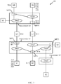
- FIG. 1 depicts concerns about conventional methods and apparatus.
- data and data transport devices are represented by an alphanumeric code (e.g., W17, A16).
- the abbreviations used herein are defined by the following key:
- interconnects X0, X1, and X3 operate independently, thus there is no coordination between interconnects X0, X1, and X3 to order transactions initiated on each interconnect bus with respect to each other. Requests from a master that target a remote slave have to go through at least one round of arbitration at each of the several interconnects located between the master and the remote slave. In the exemplary transactions depicted in FIG. 1 , a bus deadlock stemming from a circular dependency occurs when conventional arbitration techniques are applied to the following sequence of data transfers.
- Master M0 sends requests having addresses A00, A01 , A02, and A03 to slave SI via master port MPT0, arbiter ARB2, interconnect X0, link L0, master port MPT4, arbiter ARB 1, and interconnect XI. Master M0 also sends a request having the addresses A04 to slave SO via master port MPT0, arbiter ARB0, and interconnect X0. Request address A00 of master M0 wins a first stage of arbitration in arbiter ARB 2 at interconnect X0, yet address A00 must go through a second stage of arbitration in arbiter ARB 1 at interconnect XI.
- Master M1 sends requests having addresses A19 to slave SI via master port MPT1, arbiter ARB1, and interconnect X1. Master M1 also sends a request having address A15, A16, A17 and A18 to slave SO via master port MPT1, arbiter ARB3, interconnect XI, link LI , master port MPT5, arbiter ARB0, and interconnect X0.
- the request having address A19 is ahead of requests having addresses A00, A01 , A02, and A03 at the slave S 1. Further, the request having the address A04 is ahead of requests having addresses A15, A16, A17, and A18 at the slave S0.
- Master M0 attempts to send data having addresses WO0, WO1, W02, and W03 to slave S1 via master port MPT0, arbiter ARB2, interconnect X0, link L0, master port MPT4, arbiter ARB1, and interconnect X1. Master M0 also attempts to send data having the address W04 to slave SO via master port MPT0, arbiter ARB0, and interconnect X0.
- write data W04 is stuck behind data having addresses WO0, WO1, W02, and W03 in the master M0, thus the corresponding request having address A04 at slave SO cannot be fulfilled.
- Master M1 attempts to send data having addresses W15, W16, W17, and W18 to slave SO via master port MPT1, arbiter ARB1, and interconnect X1. Master M1 also attempts to send data having address W19 to slave S1 via master port MPT1, arbiter ARB3, interconnect X1, link L1, master port MPT5, arbiter ARB0, and interconnect X0.
- write data W19 is stuck behind data having addresses W15, W16, W17, and W18 in the master M1, thus the corresponding request having address A19 at slave SI cannot be fulfilled.
- applying conventional arbitration techniques results in a bus deadlock stemming from a circular dependency.
- US 2011/035523 A1 discloses a communication infrastructure for a data processing apparatus.
- WO 99/50753 A1 discloses method and apparatus for arbitrating access to multiple buses in a data processing system.
- An exemplary method includes defining a customized routing rule for data transport between a plurality of masters and a plurality of slaves via a plurality of interconnects, based on a network topology and a traffic profile.
- the defining of the customized routing table can be static or dynamic.
- the customized rule can allow a request address to arbitrate in a first phase of arbitration at an interconnect in the plurality of interconnects prior to receiving write data associated with the request address at the interconnect, and does not allow the request address to arbitrate during a subsequent second phase of arbitration unless the request address has corresponding write data.
- the customized rule can allow a first request address and a second request address to arbitrate at an interconnect in the plurality of interconnects prior to receiving respective write data associated with the first and second request addresses at the interconnect, where the first and second request addresses both target remote slaves. Further, the customized rule can block a local slave request address targeting a local slave until remote slave write data has been removed from a respective master port of an interconnect in the plurality of interconnects, if a remote slave address request targets a remote slave and the local slave address request is subsequent to the remote slave address request.
- the customized rule blocks a remote slave address request until after a local slave's write data is removed from a respective master port on an interconnect in the plurality of interconnects, if a local slave address request associated with the local slave's write data targets a local slave, the remote slave address request targets a remote slave, and the remote slave address request is received subsequent to the local slave address request.
- a non-transitory computer-readable medium comprising instructions stored thereon that, if executed by a processor, cause the processor to execute at least a part of the aforementioned method.
- the non-transitory computer-readable medium can be integrated with a device, such as a mobile device, a music player, a video player, an entertainment unit, a navigation device, a communications device, a personal digital assistant (PDA), a fixed location data unit, and/or a computer.
- a device such as a mobile device, a music player, a video player, an entertainment unit, a navigation device, a communications device, a personal digital assistant (PDA), a fixed location data unit, and/or a computer.
- PDA personal digital assistant
- an apparatus configured to mitigate bus deadlocks.
- the apparatus includes means for defining a customized routing rule for data transport between a plurality of masters and a plurality of slaves via a plurality of interconnects, based on a network topology and a traffic profile.
- the defining of the customized routing table can be static or dynamic.
- the customized rule can allow a request address to arbitrate in a first phase of arbitration at an interconnect in the plurality of interconnects prior to receiving write data associated with the request address at the interconnect, and does not allow the request address to arbitrate during a subsequent second phase of arbitration unless the request address has corresponding write data.
- the customized rule can allow a first request address and a second request address to arbitrate at an interconnect in the plurality of interconnects prior to receiving respective write data associated with the first and second request addresses at the interconnect, where the first and second request addresses both target remote slaves.
- the customized rule can block a local slave request address targeting a local slave until remote slave write data has been removed from a respective master port of an interconnect in the plurality of interconnects, if a remote slave address request targets a remote slave and the local slave address request is subsequent to the remote slave address request.
- the customized rule blocks a remote slave address request until after a local slave's write data is removed from a respective master port on an interconnect in the plurality of interconnects, if a local slave address request associated with the local slave's write data targets a local slave, the remote slave address request targets a remote slave, and the remote slave address request is received subsequent to the local slave address request.
- At least a part of the apparatus can be integrated in a semiconductor die. Further, at least a part of the apparatus can be integrated with at least one of a device, such as a mobile device, a set top box, a music player, a video player, an entertainment unit, a navigation device, a communications device, a personal digital assistant (PDA), a fixed location data unit, a computer, an application specific integrated circuit, a part of a system on a chip (SoC) integrated circuit, a base station, a micro-controller, and/or a data processing device.
- a non-transitory computer-readable medium comprising instructions stored thereon that, if executed by a lithographic device, cause the lithographic device to fabricate at least a part of the apparatus.
- an apparatus configured to mitigate bus deadlocks.
- the apparatus includes a processor configured to define a customized routing rule for data transport between a plurality of masters and a plurality of slaves via a plurality of interconnects, based on a network topology and a traffic profile.
- the defining of the customized routing table can be static or dynamic.
- the customized rule can allow a request address to arbitrate in a first phase of arbitration at a first interconnect in the plurality of interconnects prior to receiving write data associated with the request address at a second interconnect in the plurality of interconnects, and does not allow the request address to arbitrate during a subsequent second phase of arbitration unless the request address beats other competing address requests.
- the customized rule can allow a first request address and a second request address to arbitrate at an interconnect in the plurality of interconnects prior to receiving respective write data associated with the first and second request addresses at the interconnect, where the first and second request addresses both target remote slaves.
- the customized rule can block a local slave request address targeting a local slave until remote slave write data has been removed from a respective master port of an interconnect in the plurality of interconnects, if a remote slave address request targets a remote slave and the local slave address request is subsequent to the remote slave address request.
- the customized rule blocks a remote slave address request until after a local slave's write data is removed from a respective master port on an interconnect in the plurality of interconnects, if a local slave address request associated with the local slave's write data targets a local slave, the remote slave address request targets a remote slave, and the remote slave address request is received subsequent to the local slave address request.
- the apparatus can be integrated with at least one of an application specific integrated circuit, a part of a system on a chip (SoC) integrated circuit, a base station, a micro-controller, and/or a data processing device.
- SoC system on a chip
- At least a part of the apparatus can be integrated in a semiconductor die. Further, at least a part of the apparatus can be integrated with at least one of a device, such as a mobile device, a set top box, a music player, a video player, an entertainment unit, a navigation device, a communications device, a personal digital assistant (PDA), a fixed location data unit, a computer, an application specific integrated circuit, a part of a system on a chip (SoC) integrated circuit, a base station, a micro-controller, and/or a data processing device.
- a device such as a mobile device, a set top box, a music player, a video player, an entertainment unit, a navigation device, a communications device, a personal digital assistant (PDA), a fixed location data unit, a computer, an application specific integrated circuit, a part of a system on a chip (SoC) integrated circuit, a base station, a micro-controller, and/or a data processing device.
- a device such
- a non-transitory computer-readable medium comprising instructions stored thereon that, if executed by a lithographic device, cause the lithographic device to fabricate at least a part of the apparatus, such as an integrated circuit comprising a processor configured to dynamically defining a customized routing rule for data transport between a plurality of masters and a plurality of slaves via a plurality of interconnects, based on a network topology and traffic profile.
- An advantage provided by the exemplary apparatuses and methods disclosed herein is a reduction in bus deadlocks over conventional devices.
- a further advantage is that the exemplary apparatuses and methods disclosed herein mitigate the effects of bus deadlocks over conventional devices.
- any reference herein to a feature using a designation such as “first,” “second,” and so forth does not limit a quantity and/or order of those features. Rather, these designations are used as a convenient method of distinguishing between two or more features and/or instances of an feature. Thus, a reference to first and second features does not require that only two features can be employed, or that the first feature must necessarily precede the second feature. Also, unless stated otherwise, a set of features can comprise one or more features. In addition, terminology of the form “at least one of: A, B, or C" used in the description or the claims can be interpreted as "A or B or C or any combination of these features.”
- the term "exemplary” means “serving as an example, instance, or illustration.” Any embodiment described as “exemplary” is not necessarily to be construed as preferred or advantageous over other embodiments. Likewise, the term “embodiments of the invention” does not require that all embodiments of the invention include the discussed feature, advantage, or mode of operation. Use of the terms “in one example,” “an example,” “in one feature,” and/or “a feature” in this specification does not necessarily refer to the same feature and/or example. Furthermore, a particular feature and/or structure can be combined with one or more other features and/or structures.
- connection means any connection or coupling, either direct or indirect, between two or more elements, and can encompass a presence of one or more intermediate elements between two elements that are “connected” or “coupled” together.
- the coupling or connection between the elements can be physical, logical, or a combination thereof.
- two elements can be considered to be “connected” or “coupled” together by the use of one or more wires, cables, and/or printed electrical connections, as well as by the use of electromagnetic energy, such as electromagnetic energy having wavelengths in the radio frequency region, the microwave region and/or the optical (both visible and invisible) region, as several non-limiting and non-exhaustive examples.
- signal can include any signal such as a data signal, audio signal, video signal, and/or a multimedia signal.
- Information and signals can be represented using any of a variety of different technologies and techniques. For example, data, instructions, process step, commands, information, signals, bits, symbols, and/or chips that are referenced in this description can be represented by voltages, currents, electromagnetic waves, magnetic fields or particles, optical fields or particles, and any combination thereof.
- mobile device includes, and is not limited to, a mobile phone, a mobile communication device, a personal digital assistant, a mobile palm-held computer, a wireless device, and/or other types of portable electronic devices typically carried by a person and/or having some form of communication capabilities (e.g., wireless, infrared, short-range radio, etc.).
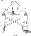
- FIG. 2 depicts an exemplary wireless communication system 200 in which an embodiment of the disclosure may be advantageously employed.
- FIG. 2 shows three remote units 220, 230, and 250, as well as two base stations 240.
- the wireless communication system 200 can have many more remote units and/or more base stations.
- the remote units 220, 230, and 250 include at least a part of an embodiment 225A-C of the disclosure as discussed further herein.
- FIG. 2 also shows forward link signals 280 from the base stations 240 to the remote units 220, 230, and 250, as well as reverse link signals 290 from the remote units 220, 230, and 250 to the base stations 240.
- the remote unit 220 is shown as a mobile telephone
- the remote unit 230 is shown as a portable computer
- the remote unit 250 is shown as a fixed location remote unit in a wireless local loop system.
- the remote unit 230 can be a mobile phone, a hand-held personal communication systems (PCS) unit, a portable data unit such as a personal data assistant, a GPS-enabled device, a navigation device, a settop box, a music player, a mobile device, a video player, an entertainment unit, any other device that stores and/or retrieves data or computer instructions, and/or any combination thereof.
- FIG. 2 illustrates remote units according to the teachings of the disclosure, the disclosure is not limited to these exemplary illustrated units. Embodiments of the disclosure may be suitably employed in any device that experiences the problems of the conventional techniques and/or can benefit from the advantages of the disclosed methods and devices.
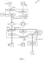
- FIG. 3 depicts an exemplary method and apparatus for transaction ordering to mitigate bus deadlocks.
- Mitigating bus deadlocks requires routing requests in an order different from that of the conventional technique. Routing requests and data from a master on one interconnect bus to a slave on another interconnect bus benefits from the transaction ordering rules described herein. Based on a topology and traffic profile, defining custom rules for each master/slave provides advantages of improving bus performance and mitigating bus deadlocks.
- one solution to address the problems of the conventional techniques is to use a customized routing rule to direct each master port coupled to an interconnect to route traffic based on a slave crossing.
- the customized routing rule can require that a master port must always block a current request from a respective master if the current request targets a different slave than a previous request from that respective master. The current request is blocked until the previous request's associated write data has been removed from the master port. This ensures requests do not get routed far on a path to the slave, in an absence of a clear path for routing the associated data to the slave. Further, no blocking of requests is done if consecutive requests target the same slave.
- request and data steering is performed by distinguishing between local slaves and remote slaves.
- slave SO is a local slave to master M0, since both local slave SO and master M0 perform data transfers to each other via the same interconnect X0 without having to transfer data via a second interconnect (e.g., interconnect X1).
- slave S1 is a remote slave for master M0, since data transfers between master M0 and slave S1 require transfer via more than one interconnect.
- slave S1 is a local slave to master M1 and slave S0 is remote slave for master M1.
- a master port MPT# e.g., a respective master port MPT for a master M#
- the request address A00 can be sent to interconnect X1 via link L0 without write data W00 in master port MPT0, but when the request address A00 reaches master port MPT4, the request address A00 must wait for the write data W00 to be available in the master port MPT4 before the request address A00 can be arbitrated (via arbiter ARB1) to be sent to slave S1.
- Two consecutive requests targeting the same or different remote slaves need not be blocked during the first phase of arbitration.
- master M3 can ping-pong consecutive requests between slave SO and slave S2 without waiting for corresponding write data to beat other queued data in arbitration.
- a master that frequently (or always) targets local slaves and/or that frequently (or always) targets remote slaves is required to follow the above rules and can dispatch requests without waiting for data to be available in a respective interconnect MPT.
- rules can be defined per master, but all rules will not always apply. In certain cases, relaxing some rules for a master and/or a slave can improve throughput.
- Hardware configured to perform the techniques described herein can self-detect network topology, traffic profiles, and data flow, and change the rule set dynamically. Defining different rules and/or sets of rules gives software flexibility to change a mode of operation.
- a master can dynamically switch ordering rules to improve network performance and mitigate bus deadlocks.
- An exemplary apparatus includes a processor coupled to at least one device depicted in FIG. 3 .
- the processor can be configured to perform at least a portion of a method described herein.
- FIG. 4 depicts an exemplary method 400 for mitigating bus deadlocks.
- the method for mitigating bus deadlocks can be performed by the apparatus described hereby, such as the apparatus depicted in FIG. 3 .
- a customized routing rule for data transport between a plurality of masters and a plurality of slaves via a plurality of interconnects is dynamically defined, based on a network topology and traffic profile.
- the customized routing rule can be at least one of the routing rules detailed herein (and can exclude conventional techniques).
- step 410 the data is routed between the plurality of interconnects using the customized routing rule.
- a circuit configured to perform at least a portion of a method described herein can be integrated with at least one of an application specific integrated circuit (ASIC), a part of a system on a chip (SoC) integrated circuit, a base station, a mobile device, a micro-controller, a data processing device, and/or a computer.
- ASIC application specific integrated circuit
- SoC system on a chip
- the teachings herein can be employed in a multiple-access system capable of supporting communication with multiple users by sharing the available system resources (e.g., by specifying one or more of bandwidth, transmit power, coding, interleaving, and so on).
- the teachings herein can be applied to any one or combinations of the following technologies: Code Division Multiple Access (CDMA) systems, Multiple-Carrier CDMA (MCCDMA), Wideband CDMA (W-CDMA), HighSpeed Packet Access (HSPA, HSPA+) systems, Time Division Multiple Access (TDMA) systems, Frequency Division Multiple Access (FDMA) systems, Single-Carrier FDMA (SC-FDMA) systems, Orthogonal Frequency Division Multiple Access (OFDMA) systems, or other multiple access techniques.
- CDMA Code Division Multiple Access
- MCCDMA Multiple-Carrier CDMA
- W-CDMA Wideband CDMA
- TDMA Time Division Multiple Access
- FDMA Frequency Division Multiple Access
- SC-FDMA Single-Carrier FDMA
- a wireless communication system employing the teachings herein can be designed to implement one or more standards, such as IS-95, cdma2000, IS-856, W-CDMA, TDSCDMA, and other standards.
- a CDMA network can implement a radio technology such as Universal Terrestrial Radio Access (UTRA), cdma2000, or some other technology.
- UTRA includes W-CDMA and Low Chip Rate (LCR).
- LCR Low Chip Rate
- the cdma2000 technology covers IS-2000, IS-95 and IS-856 standards.
- a TDMA network can implement a radio technology such as Global System for Mobile Communications (GSM).
- GSM Global System for Mobile Communications
- An OFDMA network can implement a radio technology such as Evolved UTRA (E-UTRA), IEEE 802.11, IEEE 802.16, IEEE 802.20, Flash-OFDM.RTM., etc.
- E-UTRA Evolved UTRA
- GSM are part of Universal Mobile Telecommunication System (UMTS).
- the teachings herein can be implemented in a 3GPP Long Term Evolution (LTE) system, an Ultra-Mobile Broadband (UMB) system, and other types of systems.
- LTE is a release of UMTS that uses E-UTRA.
- UTRA, E-UTRA, GSM, UMTS and LTE are described in documents from an organization named "3rd Generation Partnership Project” (3GPP), while cdma2000 is described in documents from an organization named “3rd Generation Partnership Project 2" (3GPP2).
- 3GPP 3rd Generation Partnership Project
- 3GPP2 3rd Generation Partnership Project2
- the techniques can be used in emerging and future networks and interfaces, including Long Term Evolution (LTE).
- a processor includes multiple discrete hardware components.
- a software module may reside in RAM memory, flash memory, ROM memory, EPROM memory, EEPROM memory, registers, hard disk, a removable disk, a CD-ROM, and/or any other form of storage medium known in the art.
- An exemplary storage medium can be coupled to a processor such that the processor can read information from, and write information to, the storage medium. In an alternative, the storage medium can be integral with the processor.
- An embodiment of the invention can include a computer readable media embodying a method described herein.
- Embodiments can include a machine-readable media and/or a computer-readable media embodying instructions which, when executed by a processor, transform a processor and any other cooperating devices into a machine for performing a function described hereby.
- the disclosed devices and methods can be designed and can be configured into a computer-executable file that is in a Graphic Database System Two (GDSII) compatible format, an Open Artwork System Interchange Standard (OASIS) compatible format, and/or a GERBER (e.g., RS-274D, RS-274X, etc.) compatible format, which are stored on a computer-readable media.
- the file can be provided to a fabrication handler who uses the file to fabricate an integrated device with a lithographic device.
- the integrated device is fabricated on a semiconductor wafer.
- the semiconductor wafer can be cut into a semiconductor die and packaged into a semiconductor chip.
- the semiconductor chip can be employed in a device described herein (e.g., a mobile device).
Landscapes
- Engineering & Computer Science (AREA)
- General Engineering & Computer Science (AREA)
- Theoretical Computer Science (AREA)
- Computer Hardware Design (AREA)
- Physics & Mathematics (AREA)
- General Physics & Mathematics (AREA)
- Multi Processors (AREA)
- Bus Control (AREA)
- Mobile Radio Communication Systems (AREA)
- Information Transfer Systems (AREA)
- Small-Scale Networks (AREA)
Priority Applications (1)
| Application Number | Priority Date | Filing Date | Title |
|---|---|---|---|
| EP15158870.4A EP2899642A1 (en) | 2012-01-23 | 2013-01-23 | Transaction ordering to avoid bus deadlocks |
Applications Claiming Priority (3)
| Application Number | Priority Date | Filing Date | Title |
|---|---|---|---|
| US201261589582P | 2012-01-23 | 2012-01-23 | |
| US13/669,629 US20130191572A1 (en) | 2012-01-23 | 2012-11-06 | Transaction ordering to avoid bus deadlocks |
| PCT/US2013/022785 WO2013112612A1 (en) | 2012-01-23 | 2013-01-23 | Transaction ordering to avoid bus deadlocks |
Related Child Applications (2)
| Application Number | Title | Priority Date | Filing Date |
|---|---|---|---|
| EP15158870.4A Division-Into EP2899642A1 (en) | 2012-01-23 | 2013-01-23 | Transaction ordering to avoid bus deadlocks |
| EP15158870.4A Division EP2899642A1 (en) | 2012-01-23 | 2013-01-23 | Transaction ordering to avoid bus deadlocks |
Publications (2)
| Publication Number | Publication Date |
|---|---|
| EP2807569A1 EP2807569A1 (en) | 2014-12-03 |
| EP2807569B1 true EP2807569B1 (en) | 2017-09-13 |
Family
ID=48798191
Family Applications (2)
| Application Number | Title | Priority Date | Filing Date |
|---|---|---|---|
| EP13707467.0A Not-in-force EP2807569B1 (en) | 2012-01-23 | 2013-01-23 | Transaction ordering to avoid bus deadlocks |
| EP15158870.4A Withdrawn EP2899642A1 (en) | 2012-01-23 | 2013-01-23 | Transaction ordering to avoid bus deadlocks |
Family Applications After (1)
| Application Number | Title | Priority Date | Filing Date |
|---|---|---|---|
| EP15158870.4A Withdrawn EP2899642A1 (en) | 2012-01-23 | 2013-01-23 | Transaction ordering to avoid bus deadlocks |
Country Status (7)
| Country | Link |
|---|---|
| US (1) | US20130191572A1 (OSRAM) |
| EP (2) | EP2807569B1 (OSRAM) |
| JP (1) | JP2015508193A (OSRAM) |
| KR (1) | KR20140125391A (OSRAM) |
| CN (1) | CN104067250A (OSRAM) |
| TW (1) | TWI489288B (OSRAM) |
| WO (1) | WO2013112612A1 (OSRAM) |
Families Citing this family (36)
| Publication number | Priority date | Publication date | Assignee | Title |
|---|---|---|---|---|
| US8885510B2 (en) | 2012-10-09 | 2014-11-11 | Netspeed Systems | Heterogeneous channel capacities in an interconnect |
| DE112014001621T5 (de) * | 2013-03-25 | 2015-12-24 | Mitsubishi Electric Corporation | Bus-Master, Bussystem und Bussteuerungsverfahren |
| US9471726B2 (en) | 2013-07-25 | 2016-10-18 | Netspeed Systems | System level simulation in network on chip architecture |
| US9473388B2 (en) | 2013-08-07 | 2016-10-18 | Netspeed Systems | Supporting multicast in NOC interconnect |
| US9294354B2 (en) * | 2013-10-24 | 2016-03-22 | Netspeed Systems | Using multiple traffic profiles to design a network on chip |
| US9699079B2 (en) | 2013-12-30 | 2017-07-04 | Netspeed Systems | Streaming bridge design with host interfaces and network on chip (NoC) layers |
| US9473415B2 (en) | 2014-02-20 | 2016-10-18 | Netspeed Systems | QoS in a system with end-to-end flow control and QoS aware buffer allocation |
| US9742630B2 (en) | 2014-09-22 | 2017-08-22 | Netspeed Systems | Configurable router for a network on chip (NoC) |
| US9571341B1 (en) | 2014-10-01 | 2017-02-14 | Netspeed Systems | Clock gating for system-on-chip elements |
| US9602464B2 (en) * | 2014-12-12 | 2017-03-21 | Intel Corporation | Apparatus, system and method for allocating identifiers to components of a control system |
| US9660942B2 (en) | 2015-02-03 | 2017-05-23 | Netspeed Systems | Automatic buffer sizing for optimal network-on-chip design |
| US9444702B1 (en) | 2015-02-06 | 2016-09-13 | Netspeed Systems | System and method for visualization of NoC performance based on simulation output |
| US9928204B2 (en) | 2015-02-12 | 2018-03-27 | Netspeed Systems, Inc. | Transaction expansion for NoC simulation and NoC design |
| US9568970B1 (en) | 2015-02-12 | 2017-02-14 | Netspeed Systems, Inc. | Hardware and software enabled implementation of power profile management instructions in system on chip |
| US10050843B2 (en) | 2015-02-18 | 2018-08-14 | Netspeed Systems | Generation of network-on-chip layout based on user specified topological constraints |
| US10348563B2 (en) | 2015-02-18 | 2019-07-09 | Netspeed Systems, Inc. | System-on-chip (SoC) optimization through transformation and generation of a network-on-chip (NoC) topology |
| US9864728B2 (en) | 2015-05-29 | 2018-01-09 | Netspeed Systems, Inc. | Automatic generation of physically aware aggregation/distribution networks |
| US9825809B2 (en) | 2015-05-29 | 2017-11-21 | Netspeed Systems | Dynamically configuring store-and-forward channels and cut-through channels in a network-on-chip |
| US10218580B2 (en) | 2015-06-18 | 2019-02-26 | Netspeed Systems | Generating physically aware network-on-chip design from a physical system-on-chip specification |
| US10025741B2 (en) * | 2016-01-13 | 2018-07-17 | Samsung Electronics Co., Ltd. | System-on-chip, mobile terminal, and method for operating the system-on-chip |
| US10452124B2 (en) | 2016-09-12 | 2019-10-22 | Netspeed Systems, Inc. | Systems and methods for facilitating low power on a network-on-chip |
| KR20180062807A (ko) | 2016-12-01 | 2018-06-11 | 삼성전자주식회사 | 시스템 인터커넥트 및 이를 포함하는 시스템 온 칩 |
| US20180159786A1 (en) | 2016-12-02 | 2018-06-07 | Netspeed Systems, Inc. | Interface virtualization and fast path for network on chip |
| US10313269B2 (en) | 2016-12-26 | 2019-06-04 | Netspeed Systems, Inc. | System and method for network on chip construction through machine learning |
| US10063496B2 (en) | 2017-01-10 | 2018-08-28 | Netspeed Systems Inc. | Buffer sizing of a NoC through machine learning |
| US10084725B2 (en) | 2017-01-11 | 2018-09-25 | Netspeed Systems, Inc. | Extracting features from a NoC for machine learning construction |
| US10469337B2 (en) | 2017-02-01 | 2019-11-05 | Netspeed Systems, Inc. | Cost management against requirements for the generation of a NoC |
| US10298485B2 (en) | 2017-02-06 | 2019-05-21 | Netspeed Systems, Inc. | Systems and methods for NoC construction |
| US20190020586A1 (en) * | 2017-07-14 | 2019-01-17 | Qualcomm Incorporated | Selective insertion of a deadlock recovery buffer in a bus interconnect for deadlock recovery |
| US10896476B2 (en) | 2018-02-22 | 2021-01-19 | Netspeed Systems, Inc. | Repository of integration description of hardware intellectual property for NoC construction and SoC integration |
| US10547514B2 (en) | 2018-02-22 | 2020-01-28 | Netspeed Systems, Inc. | Automatic crossbar generation and router connections for network-on-chip (NOC) topology generation |
| US11144457B2 (en) | 2018-02-22 | 2021-10-12 | Netspeed Systems, Inc. | Enhanced page locality in network-on-chip (NoC) architectures |
| US10983910B2 (en) | 2018-02-22 | 2021-04-20 | Netspeed Systems, Inc. | Bandwidth weighting mechanism based network-on-chip (NoC) configuration |
| US11176302B2 (en) | 2018-02-23 | 2021-11-16 | Netspeed Systems, Inc. | System on chip (SoC) builder |
| US11023377B2 (en) | 2018-02-23 | 2021-06-01 | Netspeed Systems, Inc. | Application mapping on hardened network-on-chip (NoC) of field-programmable gate array (FPGA) |
| FR3094810B1 (fr) | 2019-04-03 | 2023-01-13 | Thales Sa | Système sur puce comprenant une pluralité de ressources maitre |
Family Cites Families (11)
| Publication number | Priority date | Publication date | Assignee | Title |
|---|---|---|---|---|
| EP0535822B1 (en) * | 1991-09-27 | 1997-11-26 | Sun Microsystems, Inc. | Methods and apparatus for locking arbitration on a remote bus |
| US5673399A (en) * | 1995-11-02 | 1997-09-30 | International Business Machines, Corporation | System and method for enhancement of system bus to mezzanine bus transactions |
| US6260093B1 (en) * | 1998-03-31 | 2001-07-10 | Lsi Logic Corporation | Method and apparatus for arbitrating access to multiple buses in a data processing system |
| US6745272B2 (en) * | 2001-04-04 | 2004-06-01 | Advanced Micro Devices, Inc. | System and method of increasing bandwidth for issuing ordered transactions into a distributed communication system |
| US7743223B2 (en) * | 2003-08-18 | 2010-06-22 | Cray Inc. | Decoupling of write address from its associated write data in a store to a shared memory in a multiprocessor system |
| CN100538881C (zh) * | 2005-04-29 | 2009-09-09 | 台湾积体电路制造股份有限公司 | 可配置逻辑存储块 |
| US8082426B2 (en) * | 2008-11-06 | 2011-12-20 | Via Technologies, Inc. | Support of a plurality of graphic processing units |
| NL2003699A (en) * | 2008-12-18 | 2010-06-21 | Brion Tech Inc | Method and system for lithography process-window-maximixing optical proximity correction. |
| US8698823B2 (en) * | 2009-04-08 | 2014-04-15 | Nvidia Corporation | System and method for deadlock-free pipelining |
| US8285912B2 (en) * | 2009-08-07 | 2012-10-09 | Arm Limited | Communication infrastructure for a data processing apparatus and a method of operation of such a communication infrastructure |
| US20130054852A1 (en) * | 2011-08-24 | 2013-02-28 | Charles Fuoco | Deadlock Avoidance in a Multi-Node System |
-
2012
- 2012-11-06 US US13/669,629 patent/US20130191572A1/en not_active Abandoned
-
2013
- 2013-01-23 KR KR1020147023269A patent/KR20140125391A/ko not_active Withdrawn
- 2013-01-23 EP EP13707467.0A patent/EP2807569B1/en not_active Not-in-force
- 2013-01-23 TW TW102102519A patent/TWI489288B/zh not_active IP Right Cessation
- 2013-01-23 JP JP2014553538A patent/JP2015508193A/ja active Pending
- 2013-01-23 WO PCT/US2013/022785 patent/WO2013112612A1/en not_active Ceased
- 2013-01-23 EP EP15158870.4A patent/EP2899642A1/en not_active Withdrawn
- 2013-01-23 CN CN201380006136.7A patent/CN104067250A/zh active Pending
Non-Patent Citations (1)
| Title |
|---|
| None * |
Also Published As
| Publication number | Publication date |
|---|---|
| WO2013112612A1 (en) | 2013-08-01 |
| TWI489288B (zh) | 2015-06-21 |
| CN104067250A (zh) | 2014-09-24 |
| US20130191572A1 (en) | 2013-07-25 |
| EP2899642A1 (en) | 2015-07-29 |
| JP2015508193A (ja) | 2015-03-16 |
| TW201346575A (zh) | 2013-11-16 |
| EP2807569A1 (en) | 2014-12-03 |
| KR20140125391A (ko) | 2014-10-28 |
Similar Documents
| Publication | Publication Date | Title |
|---|---|---|
| EP2807569B1 (en) | Transaction ordering to avoid bus deadlocks | |
| AU2014318238B2 (en) | Ascertaining command completion in flash memories | |
| US9053058B2 (en) | QoS inband upgrade | |
| EP1645968A1 (en) | Multi-threaded DMA | |
| WO2003001388A1 (en) | System and method for controlling bus arbitration during cache memory burst cycles | |
| US9984014B2 (en) | Semiconductor device | |
| US10019380B2 (en) | Providing memory management functionality using aggregated memory management units (MMUs) | |
| JP2002073527A (ja) | Dmaコントローラ | |
| CN112470120A (zh) | 在基于矢量处理器的设备中提供对处理元件(pe)的可重构融合 | |
| EP3191971B1 (en) | Bridging strongly ordered write transactions to devices in weakly ordered domains, and related apparatuses, methods, and computer-readable media | |
| US10185684B2 (en) | System interconnect and operating method of system interconnect | |
| JP2006195746A (ja) | マルチレイヤバスシステム | |
| US7930456B1 (en) | Data packet arbitration system | |
| JPH09153009A (ja) | 階層構成バスのアービトレーション方法 | |
| US9916243B2 (en) | Method and apparatus for performing a bus lock and translation lookaside buffer invalidation | |
| US11782834B2 (en) | System and method for round robin arbiters in a network-on-chip (NoC) | |
| CN121002484A (zh) | 为基于处理器的设备中的时间敏感仲裁决策提供多请求仲裁授权策略 | |
| CN103201728B (zh) | 基于与流事务有关的信息来仲裁流事务 | |
| Purantra et al. | A Novel Approach to Solve Deadlock Problem in On-Chip BUS Communication | |
| WO2007052181A1 (en) | System-on-chip apparatus with time shareable memory and method for operating such an apparatus | |
| JPH02144751A (ja) | ダイレクトメモリアクセス回路 | |
| HK1222239B (en) | Ascertaining command completion in flash memories |
Legal Events
| Date | Code | Title | Description |
|---|---|---|---|
| PUAI | Public reference made under article 153(3) epc to a published international application that has entered the european phase |
Free format text: ORIGINAL CODE: 0009012 |
|
| 17P | Request for examination filed |
Effective date: 20140620 |
|
| AK | Designated contracting states |
Kind code of ref document: A1 Designated state(s): AL AT BE BG CH CY CZ DE DK EE ES FI FR GB GR HR HU IE IS IT LI LT LU LV MC MK MT NL NO PL PT RO RS SE SI SK SM TR |
|
| DAX | Request for extension of the european patent (deleted) | ||
| 17Q | First examination report despatched |
Effective date: 20150623 |
|
| GRAP | Despatch of communication of intention to grant a patent |
Free format text: ORIGINAL CODE: EPIDOSNIGR1 |
|
| INTG | Intention to grant announced |
Effective date: 20170324 |
|
| GRAJ | Information related to disapproval of communication of intention to grant by the applicant or resumption of examination proceedings by the epo deleted |
Free format text: ORIGINAL CODE: EPIDOSDIGR1 |
|
| GRAL | Information related to payment of fee for publishing/printing deleted |
Free format text: ORIGINAL CODE: EPIDOSDIGR3 |
|
| GRAS | Grant fee paid |
Free format text: ORIGINAL CODE: EPIDOSNIGR3 |
|
| GRAR | Information related to intention to grant a patent recorded |
Free format text: ORIGINAL CODE: EPIDOSNIGR71 |
|
| INTC | Intention to grant announced (deleted) | ||
| GRAA | (expected) grant |
Free format text: ORIGINAL CODE: 0009210 |
|
| INTG | Intention to grant announced |
Effective date: 20170802 |
|
| AK | Designated contracting states |
Kind code of ref document: B1 Designated state(s): AL AT BE BG CH CY CZ DE DK EE ES FI FR GB GR HR HU IE IS IT LI LT LU LV MC MK MT NL NO PL PT RO RS SE SI SK SM TR |
|
| REG | Reference to a national code |
Ref country code: GB Ref legal event code: FG4D |
|
| REG | Reference to a national code |
Ref country code: CH Ref legal event code: EP |
|
| REG | Reference to a national code |
Ref country code: IE Ref legal event code: FG4D |
|
| REG | Reference to a national code |
Ref country code: AT Ref legal event code: REF Ref document number: 928804 Country of ref document: AT Kind code of ref document: T Effective date: 20171015 |
|
| REG | Reference to a national code |
Ref country code: DE Ref legal event code: R096 Ref document number: 602013026505 Country of ref document: DE |
|
| REG | Reference to a national code |
Ref country code: NL Ref legal event code: MP Effective date: 20170913 |
|
| REG | Reference to a national code |
Ref country code: FR Ref legal event code: PLFP Year of fee payment: 6 |
|
| REG | Reference to a national code |
Ref country code: LT Ref legal event code: MG4D |
|
| PG25 | Lapsed in a contracting state [announced via postgrant information from national office to epo] |
Ref country code: SE Free format text: LAPSE BECAUSE OF FAILURE TO SUBMIT A TRANSLATION OF THE DESCRIPTION OR TO PAY THE FEE WITHIN THE PRESCRIBED TIME-LIMIT Effective date: 20170913 Ref country code: FI Free format text: LAPSE BECAUSE OF FAILURE TO SUBMIT A TRANSLATION OF THE DESCRIPTION OR TO PAY THE FEE WITHIN THE PRESCRIBED TIME-LIMIT Effective date: 20170913 Ref country code: HR Free format text: LAPSE BECAUSE OF FAILURE TO SUBMIT A TRANSLATION OF THE DESCRIPTION OR TO PAY THE FEE WITHIN THE PRESCRIBED TIME-LIMIT Effective date: 20170913 Ref country code: LT Free format text: LAPSE BECAUSE OF FAILURE TO SUBMIT A TRANSLATION OF THE DESCRIPTION OR TO PAY THE FEE WITHIN THE PRESCRIBED TIME-LIMIT Effective date: 20170913 Ref country code: NO Free format text: LAPSE BECAUSE OF FAILURE TO SUBMIT A TRANSLATION OF THE DESCRIPTION OR TO PAY THE FEE WITHIN THE PRESCRIBED TIME-LIMIT Effective date: 20171213 |
|
| REG | Reference to a national code |
Ref country code: AT Ref legal event code: MK05 Ref document number: 928804 Country of ref document: AT Kind code of ref document: T Effective date: 20170913 |
|
| PG25 | Lapsed in a contracting state [announced via postgrant information from national office to epo] |
Ref country code: LV Free format text: LAPSE BECAUSE OF FAILURE TO SUBMIT A TRANSLATION OF THE DESCRIPTION OR TO PAY THE FEE WITHIN THE PRESCRIBED TIME-LIMIT Effective date: 20170913 Ref country code: GR Free format text: LAPSE BECAUSE OF FAILURE TO SUBMIT A TRANSLATION OF THE DESCRIPTION OR TO PAY THE FEE WITHIN THE PRESCRIBED TIME-LIMIT Effective date: 20171214 Ref country code: ES Free format text: LAPSE BECAUSE OF FAILURE TO SUBMIT A TRANSLATION OF THE DESCRIPTION OR TO PAY THE FEE WITHIN THE PRESCRIBED TIME-LIMIT Effective date: 20170913 Ref country code: RS Free format text: LAPSE BECAUSE OF FAILURE TO SUBMIT A TRANSLATION OF THE DESCRIPTION OR TO PAY THE FEE WITHIN THE PRESCRIBED TIME-LIMIT Effective date: 20170913 Ref country code: BG Free format text: LAPSE BECAUSE OF FAILURE TO SUBMIT A TRANSLATION OF THE DESCRIPTION OR TO PAY THE FEE WITHIN THE PRESCRIBED TIME-LIMIT Effective date: 20171213 |
|
| PG25 | Lapsed in a contracting state [announced via postgrant information from national office to epo] |
Ref country code: NL Free format text: LAPSE BECAUSE OF FAILURE TO SUBMIT A TRANSLATION OF THE DESCRIPTION OR TO PAY THE FEE WITHIN THE PRESCRIBED TIME-LIMIT Effective date: 20170913 |
|
| PG25 | Lapsed in a contracting state [announced via postgrant information from national office to epo] |
Ref country code: CZ Free format text: LAPSE BECAUSE OF FAILURE TO SUBMIT A TRANSLATION OF THE DESCRIPTION OR TO PAY THE FEE WITHIN THE PRESCRIBED TIME-LIMIT Effective date: 20170913 Ref country code: RO Free format text: LAPSE BECAUSE OF FAILURE TO SUBMIT A TRANSLATION OF THE DESCRIPTION OR TO PAY THE FEE WITHIN THE PRESCRIBED TIME-LIMIT Effective date: 20170913 Ref country code: PL Free format text: LAPSE BECAUSE OF FAILURE TO SUBMIT A TRANSLATION OF THE DESCRIPTION OR TO PAY THE FEE WITHIN THE PRESCRIBED TIME-LIMIT Effective date: 20170913 |
|
| PGFP | Annual fee paid to national office [announced via postgrant information from national office to epo] |
Ref country code: GB Payment date: 20180123 Year of fee payment: 6 Ref country code: DE Payment date: 20180123 Year of fee payment: 6 |
|
| PG25 | Lapsed in a contracting state [announced via postgrant information from national office to epo] |
Ref country code: EE Free format text: LAPSE BECAUSE OF FAILURE TO SUBMIT A TRANSLATION OF THE DESCRIPTION OR TO PAY THE FEE WITHIN THE PRESCRIBED TIME-LIMIT Effective date: 20170913 Ref country code: SM Free format text: LAPSE BECAUSE OF FAILURE TO SUBMIT A TRANSLATION OF THE DESCRIPTION OR TO PAY THE FEE WITHIN THE PRESCRIBED TIME-LIMIT Effective date: 20170913 Ref country code: AT Free format text: LAPSE BECAUSE OF FAILURE TO SUBMIT A TRANSLATION OF THE DESCRIPTION OR TO PAY THE FEE WITHIN THE PRESCRIBED TIME-LIMIT Effective date: 20170913 Ref country code: SK Free format text: LAPSE BECAUSE OF FAILURE TO SUBMIT A TRANSLATION OF THE DESCRIPTION OR TO PAY THE FEE WITHIN THE PRESCRIBED TIME-LIMIT Effective date: 20170913 Ref country code: IT Free format text: LAPSE BECAUSE OF FAILURE TO SUBMIT A TRANSLATION OF THE DESCRIPTION OR TO PAY THE FEE WITHIN THE PRESCRIBED TIME-LIMIT Effective date: 20170913 Ref country code: IS Free format text: LAPSE BECAUSE OF FAILURE TO SUBMIT A TRANSLATION OF THE DESCRIPTION OR TO PAY THE FEE WITHIN THE PRESCRIBED TIME-LIMIT Effective date: 20180113 |
|
| PGFP | Annual fee paid to national office [announced via postgrant information from national office to epo] |
Ref country code: FR Payment date: 20180123 Year of fee payment: 6 |
|
| REG | Reference to a national code |
Ref country code: DE Ref legal event code: R097 Ref document number: 602013026505 Country of ref document: DE |
|
| PLBE | No opposition filed within time limit |
Free format text: ORIGINAL CODE: 0009261 |
|
| STAA | Information on the status of an ep patent application or granted ep patent |
Free format text: STATUS: NO OPPOSITION FILED WITHIN TIME LIMIT |
|
| PG25 | Lapsed in a contracting state [announced via postgrant information from national office to epo] |
Ref country code: DK Free format text: LAPSE BECAUSE OF FAILURE TO SUBMIT A TRANSLATION OF THE DESCRIPTION OR TO PAY THE FEE WITHIN THE PRESCRIBED TIME-LIMIT Effective date: 20170913 |
|
| 26N | No opposition filed |
Effective date: 20180614 |
|
| REG | Reference to a national code |
Ref country code: CH Ref legal event code: PL |
|
| PG25 | Lapsed in a contracting state [announced via postgrant information from national office to epo] |
Ref country code: LU Free format text: LAPSE BECAUSE OF NON-PAYMENT OF DUE FEES Effective date: 20180123 |
|
| REG | Reference to a national code |
Ref country code: IE Ref legal event code: MM4A |
|
| REG | Reference to a national code |
Ref country code: BE Ref legal event code: MM Effective date: 20180131 |
|
| PG25 | Lapsed in a contracting state [announced via postgrant information from national office to epo] |
Ref country code: BE Free format text: LAPSE BECAUSE OF NON-PAYMENT OF DUE FEES Effective date: 20180131 Ref country code: LI Free format text: LAPSE BECAUSE OF NON-PAYMENT OF DUE FEES Effective date: 20180131 Ref country code: SI Free format text: LAPSE BECAUSE OF FAILURE TO SUBMIT A TRANSLATION OF THE DESCRIPTION OR TO PAY THE FEE WITHIN THE PRESCRIBED TIME-LIMIT Effective date: 20170913 Ref country code: CH Free format text: LAPSE BECAUSE OF NON-PAYMENT OF DUE FEES Effective date: 20180131 |
|
| PG25 | Lapsed in a contracting state [announced via postgrant information from national office to epo] |
Ref country code: IE Free format text: LAPSE BECAUSE OF NON-PAYMENT OF DUE FEES Effective date: 20180123 |
|
| PG25 | Lapsed in a contracting state [announced via postgrant information from national office to epo] |
Ref country code: MC Free format text: LAPSE BECAUSE OF FAILURE TO SUBMIT A TRANSLATION OF THE DESCRIPTION OR TO PAY THE FEE WITHIN THE PRESCRIBED TIME-LIMIT Effective date: 20170913 |
|
| REG | Reference to a national code |
Ref country code: DE Ref legal event code: R119 Ref document number: 602013026505 Country of ref document: DE |
|
| GBPC | Gb: european patent ceased through non-payment of renewal fee |
Effective date: 20190123 |
|
| PG25 | Lapsed in a contracting state [announced via postgrant information from national office to epo] |
Ref country code: FR Free format text: LAPSE BECAUSE OF NON-PAYMENT OF DUE FEES Effective date: 20190131 Ref country code: DE Free format text: LAPSE BECAUSE OF NON-PAYMENT OF DUE FEES Effective date: 20190801 |
|
| PG25 | Lapsed in a contracting state [announced via postgrant information from national office to epo] |
Ref country code: GB Free format text: LAPSE BECAUSE OF NON-PAYMENT OF DUE FEES Effective date: 20190123 |
|
| PG25 | Lapsed in a contracting state [announced via postgrant information from national office to epo] |
Ref country code: MT Free format text: LAPSE BECAUSE OF NON-PAYMENT OF DUE FEES Effective date: 20180123 |
|
| PG25 | Lapsed in a contracting state [announced via postgrant information from national office to epo] |
Ref country code: TR Free format text: LAPSE BECAUSE OF FAILURE TO SUBMIT A TRANSLATION OF THE DESCRIPTION OR TO PAY THE FEE WITHIN THE PRESCRIBED TIME-LIMIT Effective date: 20170913 |
|
| PG25 | Lapsed in a contracting state [announced via postgrant information from national office to epo] |
Ref country code: PT Free format text: LAPSE BECAUSE OF FAILURE TO SUBMIT A TRANSLATION OF THE DESCRIPTION OR TO PAY THE FEE WITHIN THE PRESCRIBED TIME-LIMIT Effective date: 20170913 Ref country code: HU Free format text: LAPSE BECAUSE OF FAILURE TO SUBMIT A TRANSLATION OF THE DESCRIPTION OR TO PAY THE FEE WITHIN THE PRESCRIBED TIME-LIMIT; INVALID AB INITIO Effective date: 20130123 |
|
| PG25 | Lapsed in a contracting state [announced via postgrant information from national office to epo] |
Ref country code: CY Free format text: LAPSE BECAUSE OF FAILURE TO SUBMIT A TRANSLATION OF THE DESCRIPTION OR TO PAY THE FEE WITHIN THE PRESCRIBED TIME-LIMIT Effective date: 20170913 Ref country code: MK Free format text: LAPSE BECAUSE OF NON-PAYMENT OF DUE FEES Effective date: 20170913 |
|
| PG25 | Lapsed in a contracting state [announced via postgrant information from national office to epo] |
Ref country code: AL Free format text: LAPSE BECAUSE OF FAILURE TO SUBMIT A TRANSLATION OF THE DESCRIPTION OR TO PAY THE FEE WITHIN THE PRESCRIBED TIME-LIMIT Effective date: 20170913 |