EP2807568B1 - Verfahren zur verwaltung von speicherzugriffsanforderungen und datenspeichersystem - Google Patents
Verfahren zur verwaltung von speicherzugriffsanforderungen und datenspeichersystem Download PDFInfo
- Publication number
- EP2807568B1 EP2807568B1 EP13702618.3A EP13702618A EP2807568B1 EP 2807568 B1 EP2807568 B1 EP 2807568B1 EP 13702618 A EP13702618 A EP 13702618A EP 2807568 B1 EP2807568 B1 EP 2807568B1
- Authority
- EP
- European Patent Office
- Prior art keywords
- request
- requests
- processing stage
- clock cycle
- new
- Prior art date
- Legal status (The legal status is an assumption and is not a legal conclusion. Google has not performed a legal analysis and makes no representation as to the accuracy of the status listed.)
- Active
Links
Images
Classifications
-
- G—PHYSICS
- G11—INFORMATION STORAGE
- G11C—STATIC STORES
- G11C7/00—Arrangements for writing information into, or reading information out from, a digital store
- G11C7/10—Input/output [I/O] data interface arrangements, e.g. I/O data control circuits, I/O data buffers
- G11C7/1072—Input/output [I/O] data interface arrangements, e.g. I/O data control circuits, I/O data buffers for memories with random access ports synchronised on clock signal pulse trains, e.g. synchronous memories, self timed memories
-
- G—PHYSICS
- G06—COMPUTING OR CALCULATING; COUNTING
- G06F—ELECTRIC DIGITAL DATA PROCESSING
- G06F12/00—Accessing, addressing or allocating within memory systems or architectures
- G06F12/02—Addressing or allocation; Relocation
- G06F12/06—Addressing a physical block of locations, e.g. base addressing, module addressing, memory dedication
-
- G—PHYSICS
- G06—COMPUTING OR CALCULATING; COUNTING
- G06F—ELECTRIC DIGITAL DATA PROCESSING
- G06F12/00—Accessing, addressing or allocating within memory systems or architectures
- G06F12/02—Addressing or allocation; Relocation
- G06F12/08—Addressing or allocation; Relocation in hierarchically structured memory systems, e.g. virtual memory systems
- G06F12/0802—Addressing of a memory level in which the access to the desired data or data block requires associative addressing means, e.g. caches
- G06F12/0844—Multiple simultaneous or quasi-simultaneous cache accessing
-
- G—PHYSICS
- G06—COMPUTING OR CALCULATING; COUNTING
- G06F—ELECTRIC DIGITAL DATA PROCESSING
- G06F12/00—Accessing, addressing or allocating within memory systems or architectures
- G06F12/02—Addressing or allocation; Relocation
- G06F12/08—Addressing or allocation; Relocation in hierarchically structured memory systems, e.g. virtual memory systems
- G06F12/0802—Addressing of a memory level in which the access to the desired data or data block requires associative addressing means, e.g. caches
- G06F12/0844—Multiple simultaneous or quasi-simultaneous cache accessing
- G06F12/0855—Overlapped cache accessing, e.g. pipeline
-
- G—PHYSICS
- G06—COMPUTING OR CALCULATING; COUNTING
- G06F—ELECTRIC DIGITAL DATA PROCESSING
- G06F13/00—Interconnection of, or transfer of information or other signals between, memories, input/output devices or central processing units
- G06F13/14—Handling requests for interconnection or transfer
- G06F13/16—Handling requests for interconnection or transfer for access to memory bus
- G06F13/1605—Handling requests for interconnection or transfer for access to memory bus based on arbitration
- G06F13/161—Handling requests for interconnection or transfer for access to memory bus based on arbitration with latency improvement
- G06F13/1615—Handling requests for interconnection or transfer for access to memory bus based on arbitration with latency improvement using a concurrent pipeline structrure
-
- G—PHYSICS
- G06—COMPUTING OR CALCULATING; COUNTING
- G06F—ELECTRIC DIGITAL DATA PROCESSING
- G06F9/00—Arrangements for program control, e.g. control units
- G06F9/06—Arrangements for program control, e.g. control units using stored programs, i.e. using an internal store of processing equipment to receive or retain programs
- G06F9/30—Arrangements for executing machine instructions, e.g. instruction decode
- G06F9/38—Concurrent instruction execution, e.g. pipeline or look ahead
- G06F9/3836—Instruction issuing, e.g. dynamic instruction scheduling or out of order instruction execution
-
- G—PHYSICS
- G06—COMPUTING OR CALCULATING; COUNTING
- G06F—ELECTRIC DIGITAL DATA PROCESSING
- G06F2212/00—Indexing scheme relating to accessing, addressing or allocation within memory systems or architectures
- G06F2212/10—Providing a specific technical effect
- G06F2212/1016—Performance improvement
- G06F2212/1024—Latency reduction
Definitions
- the present invention relates to a method for managing access requests to memories and a data storage system.
- DSPs digital signal processors
- SIMD single-statement processors on multiple data
- LIW Long Instruction Word
- vector processors that is, designed to perform operations on multiple numbers (representing vectors or matrices) during a single clock cycle.
- Such processors need to be able to read and write a set of data at the same time as quickly as possible.
- Each memory has a number of input and output ports. Each input port is intended to receive a request to access one of the memory locations, identified by its address, called local address, in the memory.
- the memory is for receiving local requests at each clock cycle and responding to them in a predetermined number of clock cycles.
- the memory is also intended to present, at the end of this or these clock cycles, the possible responses on its output ports.
- a memory can receive a limited number of local requests per clock cycle, at most equal to the number of input ports of this memory.
- a typical type of memory is for example a random access memory (called “Random Access Memory” or RAM in English) simple port (an input port and an associated output port) or dual ports (two ports of entry and two associated output ports).
- Random Access Memory Random Access Memory
- simple port an input port and an associated output port
- dual ports two ports of entry and two associated output ports
- the storage system further includes input ports and one or more output ports. Each input port is intended to receive, at each clock cycle, a request for access to a location of one of the memories.
- This query indicates a structured global address as if the storage system constituted a single memory. It is thus known to use a mapping function that associates each global address with one of the memories and with a local address in this memory.
- the storage system receives on its input ports a number of access requests to the same memory greater than this memory can receive on its ports. 'Entrance. There is therefore a conflict because the memory will not be able to receive all these requests in the same clock cycle.
- the document US 6,788,585 B1 discloses a memory array having a clock, a sense amplifier control gate, and a sense amplifier.
- the memory array receives a request from a processor and this request is transmitted to the memory array.
- the sense amplifier control gate uses a read activation input to selectively enable or disable the sense amplifier to control whether new read data propagates from the memory array.
- the storage system 100 firstly includes a clock signal input CLK for receiving a timing clock signal from the storage system 100.
- the clock signal defines successive clock cycles.
- Each memory 102 n has one or more input ports generally designated 104 n and one or more output ports generally designated 106 n .
- Each input port 104 n of each memory 102 n is intended to receive, at each clock cycle, at most one access request to the memory 102 n .
- This request is in the form of a local request indicating in particular an address of the memory 102 n where the access is intended to be realized.
- Each input port 104 is for receiving n of read access requests and write, or specialized to receive only read access requests or as write access requests.
- Each output port 106 n of each memory 102 n is associated with a single input port 104 n and is intended to present, at each clock cycle, at most one response to a request obtained from the input port 104 not associated. In the example described, only the read requests are intended to give rise to a response, but not the write requests. Thus, an output port 106 n is associated with each input port 104 n for receiving at least one of read access requests, but there are no associated output port to the input ports 104 n specialized in writing.
- Each memory 102 n is thus intended, at each clock cycle, to obtain requests from its input ports 104 n, to perform, and to provide its output ports 106 n possible responses. Since the input ports 104 n are in limited number, each memory 102 n is able to obtain only a limited number of requests at each clock cycle, which will be called thereafter "capacity" of the memory .
- the execution of the requests takes several clock cycles.
- the storage system 100 further comprises at least two input ports generally designated 108 and one or more output ports generally designated 110.
- Each input port 108 is intended to receive, at each clock cycle, at most one access request to one of the memories 102 n .
- This request is in the form of a global query indicating in particular a structured global address as if the storage system 100 was a single memory.
- Each input port 108 is intended to receive requests for read and write access, or specialized to receive only read access requests or write access requests.
- Each output port 110 is associated with a single input port 108 and is intended to present, at each clock cycle, at most one response to a request obtained from the associated input port 108. In the example described, only the read requests are intended to give rise to a response, but not the write requests. Thus, an output port 110 is associated with each input port 108 intended to receive at least read access requests, but there is no output port associated with the input ports 108 specialized in writing .
- the storage system 100 further comprises one or more processing stages for successively processing the requests obtained from the input ports 108, to realize them and, if necessary, to provide a response.
- the treatment stage or stages are intended to be successively traversed so as to form a processing line (translation of the English " pipeline ").
- each processing stage is intended to process the data it receives in a clock cycle.
- it is intended to receive, at each clock cycle, input data and to provide the output data corresponding to the input data before the next clock cycle.
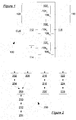
- the storage system 100 comprises three processing stages: a request processing stage 112, an intermediate stage 114 grouping the memories 102 n and an output stage 116 for processing the responses.
- the input stage 112 is intended, at each clock cycle, to carry out the steps which will be detailed with reference to the figure 2 .
- the input stage 112 is intended to obtain requests from the input ports 108, to select some of them, and to provide the selected requests to the intermediate stage 114, that is to say to the input ports 104 n of memories 102 n .
- the requests are provided in the form of local requests indicating a local address in the memory 102 n where the reading or writing is intended to be performed.
- the input stage 112 includes a correspondence function F associating each possible global address to one of the memories 102 n and to a local address in this memory 102 n .
- the output stage 116 is intended, at each clock cycle, to carry out the steps which will be detailed with reference to the figure 2 .
- the output stage 116 is intended to obtain from the output ports 106 n of the memories 102 n the possible responses provided by the memories 102 n , to determine, for each possible response, the output port 110 on which the response is intended to be provided, and to provide this response on this output port 110.
- the storage system 100 is realized only with hardware components, and not with software components such as processors executing instructions stored on a storage medium.
- a priority request is a request placed on hold at each of the last L clock cycles starting from the previous clock cycle, L being a predetermined number greater than or equal to two.
- the input stage 112 determines, by means of the addressing function F, the memory 102 n and the local address in this memory referred to by the new request. .
- the input stage 112 abstains from obtaining new requests.
- the input stage 112 selects, from among the possible pending requests and the possible new request or requests, at least one request intended to be provided to the intermediate stage 114.
- the selection of at least one request is made according to the capacity of each memory 102 n to obtain requests. In particular, for each memory 102 n , a number of requests less than or equal to the number of input port 104 n of the memory 102 n is selected.
- the selection is made so as to select the largest possible number of requests that the memory will be able to receive the next clock cycle.
- the selection of at least one request is made by giving priority to the oldest queued requests, that is to say the queries queued for the largest number of clock cycles.
- the input stage 112 selects at least one new request.
- the input stage 112 selects at least one pending request and no new request (since no new request has been received in the cycle of delay). current clock).
- the input stage 112 supplies each selected request to an input port 104 n of the memory 102 n targeted by this request.
- the request is provided in the form of a local request indicating in particular the targeted local address.
- the input stage 112 puts on hold the unselected request (s).
- this new request is put on hold.
- the input stage 112 determines the existence or not of at least one request put on hold since at least L clock cycles, including the current clock cycle, c that is, put on hold at each of the last L clock cycles, including the current clock cycle.
- L is a predetermined number greater than or equal to two.
- Such a request is qualified as a priority.
- the storage system 100 is then in a situation called conflict.
- the input stage 112 suspends obtaining new requests for the next clock cycle.
- the input stage 112 also prevents the computer device (not shown) providing the requests to the storage system 100 of this conflict situation, so that the latter, for example, suspends the sending of requests to the system. storage 100 for the next clock cycle.
- each memory 102 n obtains on its input ports 104 n the requests that were provided to it in the previous cycle in the form of a local request by the input stage 112.
- each memory 102 n processes the requests it has obtained. In particular, in the case of an access request in writing indicating data to write, the memory 102 n writes this data to the local address. In the case of a read request, the memory 102 n reads the data at the local address.
- each memory 102 n provides the possible responses on its output ports 106 n .
- the memory 102 n supplies the data read from its output port 106 n associated with the input port 104 n on which the request was obtained.
- the output stage 116 obtains, from the output ports 106 n of the memories 102 n , the possible responses provided by the memories 102 n .
- the output stage 116 determines, for each possible response, the output port 110 on which the response is intended to be provided.
- the output stage 116 provides each response on the output port 110 associated with the input port 108 on which the request corresponding to this response has been received.
- the storage system 100 comprises three input ports 108 (intended to receive read and write access requests).
- the predetermined number L is two, so that a request on hold two consecutive clock cycles becomes a priority and causes the stop of obtaining new requests.
- the left box of the first row of the table indicates the new requests obtained on the input ports 108 at the current clock cycle.
- the box on the right of the first row of the table indicates queries that are waiting, that is, put on hold at the clock cycle preceding the current clock cycle.
- the right-hand box of the second row of the table indicates the queries selected at the current clock cycle to be supplied to the intermediate stage 114.
- the left-hand box in the second row of the table indicates queries that are queued at the current clock cycle.
- a request determined as a priority at the end of the current clock cycle is indicated by an underline.
- Queries are written in the form: Xy (n) where X is a letter corresponding to the input port (A for the first port, B for the second, and C for the third), y is the number of the request and n is the index of the reference of the memory 102 n referred to by the request.
- the input stage 112 obtains new requests, provides two new requests to the intermediate stage and puts on hold a new request.
- the input stage 112 obtains new requests, selects two requests from the new requests and the pending request and provides these two requests.
- One of the two selected queries is a new query obtained in the second clock cycle.
- A3 (2), B3 (3), C3 (3) A2 (1), B2 (1) A2 (1), A3 (2), B3 (3) B2 (1) , C3 (3)
- the input stage 112 determines the existence of a priority request.
- the input stage suspends obtaining new requests, and provides the priority request and a non-priority request.
- the storage system 100 and the management method 200 it was calculated the ratio between, on the one hand, the number of clock cycles where no new request is obtained. because of the presence of at least priority request to the previous clock cycle and, secondly, the number of clock cycles where new requests are obtained because of the absence of priority request to the cycle of previous clock.
Landscapes
- Engineering & Computer Science (AREA)
- Theoretical Computer Science (AREA)
- Physics & Mathematics (AREA)
- General Engineering & Computer Science (AREA)
- General Physics & Mathematics (AREA)
- Software Systems (AREA)
- Multi Processors (AREA)
Claims (8)
- Verfahren zur Verwaltung von Anforderungen, erhalten von einem Speichersystem (100), aufweisend Speicher (102n), die jeweils einen oder mehrere Eingangsports (104n) und einen oder mehrere Ausgangsports (106n) aufweisen, einen Eingang (CLK), der zum Empfangen eines Zeitsignals bestimmt ist, das aufeinanderfolgende Zeitzyklen festlegt, und eine Verarbeitungsstufe (112), wobei das Speichersystem (100) zum Empfangen von Anforderungen bestimmt ist, die jeweils einen Zugriff auf eine Stelle einer der Speicher (102n) anfordern, wobei das Verfahren bei einem ersten Zeitzyklus aufweist:- Erhalten (202) neuer Anforderungen durch die Verarbeitungsstufe (112),- Bereitstellen (210), durch die Verarbeitungsstufe (112), von mindestens einer der neuen Anforderungen,- Versetzen in Warteposition (212), durch die Verarbeitungsstufe (112), von mindestens einer anderen der neuen Anforderungen, im Folgenden Anforderung in Warteposition genannt,wobei das Verfahren dadurch gekennzeichnet ist, dass es bei einem zweiten Zeitzyklus, der dem ersten Zeitzyklus folgt, aufweist:- Erhalten (202), durch die Verarbeitungsstufe (112), von mindestens einer neuen Anforderung,- Auswählen (208), durch die Verarbeitungsstufe (112), aus der oder den Anforderungen in Warteposition und der oder den neuen Anforderungen mindestens einer Anforderung,- Bereitstellen (210), durch die Verarbeitungsstufe, der ausgewählten Anforderung(en),und dadurch, dass es ferner aufweist:- Ermitteln (214) des Vorhandenseins oder nicht einer in Warteposition versetzten Anforderung bei jedem der L Zeitzyklen vor dem laufenden Zeitzyklus, wobei L eine bestimmte Anzahl größer oder gleich zwei ist, wobei eine derartige Anforderung prioritäre Anforderung genannt wird,wenn das Vorhandensein von mindestens einer prioritären Anforderung ermittelt ist, das Aussetzen des Erhaltens von neuen Anforderungen durch die Verarbeitungsstufe (112) für den laufenden Zeitzyklus
und wobei das Erhalten (202), durch die Verarbeitungsstufe (112), von mindestens einer neuen Anforderung durchgeführt wird, wenn das Vorhandensein keiner neuen prioritären Anforderung ermittelt ist. - Verfahren nach Anspruch 1, wobei die Anforderungen durch die Verarbeitungsstufe (112) einer folgenden Verarbeitungsstufe (114) in dem Speichersystem (100) bereitgestellt werden.
- Verfahren nach Anspruch 2, wobei die folgende Verarbeitungsstufe (114) die Speicher (102n) aufweist.
- Verfahren nach einem der Ansprüche 1 bis 3, wobei das Auswählen (208), durch die Verarbeitungsstufe (112), von mindestens einer Anforderung das Auswählen einer Anforderung in Warteposition aufweist.
- Verfahren nach einem der Ansprüche 1 bis 4, wobei das Auswählen (208), durch die Verarbeitungsstufe (112), von mindestens einer Anforderung das Auswählen einer neuen, im zweiten Zeitzyklus erhaltenen Anforderung aufweist.
- Verfahren nach einem der Ansprüche 1 bis 5, wobei, für mindestens einen Speicher (102n), das Auswählen von mindestens einer Anforderung, die zur Bereitstellung bei diesem Speicher bestimmt ist, derart durchgeführt wird, dass die größtmögliche Anzahl von Anforderungen ausgewählt wird, die der Speicher imstande ist, im nächsten Zeitzyklus zu empfangen.
- Verfahren nach einem der Ansprüche 1 bis 6, wobei, für mindestens einen Speicher (102n), das Auswählen von mindestens einer Anforderung, die zur Bereitstellung bei diesem Speicher bestimmt ist, durchgeführt wird, indem den seit der größten Anzahl von Zeitzyklen in Warteposition versetzten Anforderungen Priorität gegeben wird.
- Datenspeichersystem (100) aufweisend:- Speicher (102n), die jeweils einen oder mehrere Eingangsports (104n) und einen oder mehrere Ausgangsports (106n) aufweisen, wobei das Speichersystem (100) zum Empfangen der Anforderungen bestimmt ist, die jeweils einen Zugriff auf eine Stelle einer der Speicher (102n) anfordern,- einen Eingang (CLK), der zum Empfangen eines Zeitsignals bestimmt ist, das aufeinanderfolgende Zeitzyklen festlegt,- eine Verarbeitungsstufe (112), die bei einem ersten Zeitzyklus bestimmt ist:und dadurch, dass die Verarbeitungsstufe ferner bestimmt ist, um:- neue Anforderungen zu erhalten,- mindestens eine der neuen Anforderungen bereitzustellen,- mindestens eine andere der neuen Anforderungen, im Folgenden Anforderung in Warteposition genannt, in Warteposition zu versetzen,wobei das Speichersystem (112) dadurch gekennzeichnet ist, dass die Verarbeitungsstufe ferner bestimmt ist, bei einem zweiten Zeitzyklus, der dem ersten Zeitzyklus folgt:- mindestens eine neue Anforderung zu erhalten,- aus der oder den Anforderungen in Warteposition und der oder den neuen Anforderungen mindestens eine Anforderung auszuwählen, die bestimmt ist, bereitgestellt zu werden,- die ausgewählte(n) Anforderung(en) bereitzustellen,- das Vorhandenseins oder nicht einer in Warteposition versetzten Anforderung bei jedem der L Zeitzyklen vor dem laufenden Zeitzyklus zu ermitteln (214), wobei L eine bestimmte Anzahl größer oder gleich zwei ist, wobei eine derartige Anforderung prioritäre Anforderung genannt wird,wenn das Vorhandensein von mindestens einer prioritären Anforderung ermittelt ist, Aussetzen des Erhaltens von neuen Anforderungen durch die Verarbeitungsstufe (112) für den laufenden Zeitzyklus
und wobei das Erhalten (202), durch die Verarbeitungsstufe (112), von mindestens einer neuen Anforderung durchgeführt wird, wenn das Vorhandensein keiner prioritären Anforderung ermittelt ist.
Applications Claiming Priority (2)
| Application Number | Priority Date | Filing Date | Title |
|---|---|---|---|
| FR1200248A FR2986345B1 (fr) | 2012-01-27 | 2012-01-27 | Procede de gestion de requetes d'acces a des memoires et systeme de stockage de donnees |
| PCT/EP2013/051523 WO2013110802A1 (fr) | 2012-01-27 | 2013-01-27 | Procédé de gestion de requêtes d'accès à des mémoires et système de stockage de données |
Publications (2)
| Publication Number | Publication Date |
|---|---|
| EP2807568A1 EP2807568A1 (de) | 2014-12-03 |
| EP2807568B1 true EP2807568B1 (de) | 2019-04-03 |
Family
ID=47664273
Family Applications (1)
| Application Number | Title | Priority Date | Filing Date |
|---|---|---|---|
| EP13702618.3A Active EP2807568B1 (de) | 2012-01-27 | 2013-01-27 | Verfahren zur verwaltung von speicherzugriffsanforderungen und datenspeichersystem |
Country Status (4)
| Country | Link |
|---|---|
| US (1) | US9583158B2 (de) |
| EP (1) | EP2807568B1 (de) |
| FR (1) | FR2986345B1 (de) |
| WO (1) | WO2013110802A1 (de) |
Families Citing this family (1)
| Publication number | Priority date | Publication date | Assignee | Title |
|---|---|---|---|---|
| FR2986343B1 (fr) * | 2012-01-27 | 2015-01-23 | Simpulse | Procede de pre-compilation, procede de compilation, programme d'ordinateur et systeme informatique |
Citations (1)
| Publication number | Priority date | Publication date | Assignee | Title |
|---|---|---|---|---|
| US20040088516A1 (en) * | 2002-10-30 | 2004-05-06 | Dwyer Malcolm Ryle | Virtual memory translation unit for multimedia accelerators |
Family Cites Families (5)
| Publication number | Priority date | Publication date | Assignee | Title |
|---|---|---|---|---|
| US6788585B1 (en) * | 2002-11-27 | 2004-09-07 | Cisco Technology, Inc. | System and method for processing data in a memory array |
| US7240144B2 (en) * | 2004-04-02 | 2007-07-03 | Arm Limited | Arbitration of data transfer requests |
| US20080082707A1 (en) * | 2006-09-29 | 2008-04-03 | Synfora, Inc. | Non-blocking bus controller for a pipelined, variable latency, hierarchical bus with point-to-point first-in first-out ordering |
| US7877558B2 (en) * | 2007-08-13 | 2011-01-25 | Advanced Micro Devices, Inc. | Memory controller prioritization scheme |
| US8930641B1 (en) * | 2011-06-14 | 2015-01-06 | Altera Corporation | Systems and methods for providing memory controllers with scheduler bypassing capabilities |
-
2012
- 2012-01-27 FR FR1200248A patent/FR2986345B1/fr active Active
-
2013
- 2013-01-27 US US14/375,052 patent/US9583158B2/en not_active Expired - Fee Related
- 2013-01-27 WO PCT/EP2013/051523 patent/WO2013110802A1/fr not_active Ceased
- 2013-01-27 EP EP13702618.3A patent/EP2807568B1/de active Active
Patent Citations (1)
| Publication number | Priority date | Publication date | Assignee | Title |
|---|---|---|---|---|
| US20040088516A1 (en) * | 2002-10-30 | 2004-05-06 | Dwyer Malcolm Ryle | Virtual memory translation unit for multimedia accelerators |
Also Published As
| Publication number | Publication date |
|---|---|
| EP2807568A1 (de) | 2014-12-03 |
| FR2986345B1 (fr) | 2014-02-28 |
| FR2986345A1 (fr) | 2013-08-02 |
| US20150006842A1 (en) | 2015-01-01 |
| WO2013110802A1 (fr) | 2013-08-01 |
| US9583158B2 (en) | 2017-02-28 |
Similar Documents
| Publication | Publication Date | Title |
|---|---|---|
| US8639902B2 (en) | Methods for sequencing memory access requests | |
| US10970214B2 (en) | Selective downstream cache processing for data access | |
| US8607005B2 (en) | Monitoring program execution to learn data blocks accessed by software process for facilitating efficient prefetching | |
| WO2017101642A1 (zh) | 分布式系统的数据节点升级方法及装置 | |
| WO2021056541A1 (zh) | 处理数据的方法和设备 | |
| US20070073920A1 (en) | Method of accessing internal memory of a processor and device thereof | |
| US6880057B1 (en) | Split write data processing mechanism for memory controllers utilizing inactive periods during write data processing for other transactions | |
| US20040068615A1 (en) | Apparatus, method, and system for reducing latency of memory devices | |
| FR3020885A1 (de) | ||
| EP2044524A1 (de) | Verfahren und vorrichtung für schnelle audiosuche | |
| US9378125B2 (en) | Semiconductor chip and method of controlling memory | |
| US11636056B1 (en) | Hierarchical arbitration structure | |
| US20230289063A1 (en) | Electronic system and method for controlling burst length to access memory device of electronic system | |
| WO2013110802A1 (fr) | Procédé de gestion de requêtes d'accès à des mémoires et système de stockage de données | |
| US9483401B2 (en) | Data processing method and apparatus | |
| CN119166063A (zh) | 适应于大对象分区的分区分裂管理方法及装置 | |
| CN117608661A (zh) | 一种数组表访问指令原子性保障的方法、系统及装置 | |
| CN116841700A (zh) | 数据库事务的提交方法、装置、服务器及介质 | |
| FR2964211A1 (fr) | Dispositif de controle d'acces a des memoires simple port | |
| TW202509787A (zh) | 記憶體裝置及其操作方法及非暫時性電腦可讀儲存媒體 | |
| CN120407437B (zh) | 对多个内存库快速寻找数据新老关系的方法和装置 | |
| US9645936B1 (en) | System and method for informing hardware to limit writing in a memory hierarchy | |
| WO2019046255A1 (en) | CACHE MEMORY BUFFER | |
| US20100217941A1 (en) | Improving the efficiency of files sever requests in a computing device | |
| WO2016177083A1 (zh) | 一种数据存储方法、存储装置和计算机存储介质 |
Legal Events
| Date | Code | Title | Description |
|---|---|---|---|
| PUAI | Public reference made under article 153(3) epc to a published international application that has entered the european phase |
Free format text: ORIGINAL CODE: 0009012 |
|
| 17P | Request for examination filed |
Effective date: 20140818 |
|
| AK | Designated contracting states |
Kind code of ref document: A1 Designated state(s): AL AT BE BG CH CY CZ DE DK EE ES FI FR GB GR HR HU IE IS IT LI LT LU LV MC MK MT NL NO PL PT RO RS SE SI SK SM TR |
|
| DAX | Request for extension of the european patent (deleted) | ||
| STAA | Information on the status of an ep patent application or granted ep patent |
Free format text: STATUS: EXAMINATION IS IN PROGRESS |
|
| 17Q | First examination report despatched |
Effective date: 20170728 |
|
| REG | Reference to a national code |
Ref country code: DE Ref legal event code: R079 Ref document number: 602013053237 Country of ref document: DE Free format text: PREVIOUS MAIN CLASS: G06F0013362000 Ipc: G06F0009380000 |
|
| GRAP | Despatch of communication of intention to grant a patent |
Free format text: ORIGINAL CODE: EPIDOSNIGR1 |
|
| STAA | Information on the status of an ep patent application or granted ep patent |
Free format text: STATUS: GRANT OF PATENT IS INTENDED |
|
| RIC1 | Information provided on ipc code assigned before grant |
Ipc: G06F 12/0844 20160101ALI20180921BHEP Ipc: G06F 12/06 20060101ALI20180921BHEP Ipc: G06F 12/0855 20160101ALI20180921BHEP Ipc: G06F 9/38 20060101AFI20180921BHEP Ipc: G06F 13/16 20060101ALI20180921BHEP Ipc: G11C 7/10 20060101ALI20180921BHEP |
|
| INTG | Intention to grant announced |
Effective date: 20181018 |
|
| RIC1 | Information provided on ipc code assigned before grant |
Ipc: G06F 13/16 20060101ALI20180921BHEP Ipc: G06F 12/06 20060101ALI20180921BHEP Ipc: G06F 12/0844 20160101ALI20180921BHEP Ipc: G06F 9/38 20180101AFI20180921BHEP Ipc: G11C 7/10 20060101ALI20180921BHEP Ipc: G06F 12/0855 20160101ALI20180921BHEP |
|
| GRAS | Grant fee paid |
Free format text: ORIGINAL CODE: EPIDOSNIGR3 |
|
| GRAA | (expected) grant |
Free format text: ORIGINAL CODE: 0009210 |
|
| STAA | Information on the status of an ep patent application or granted ep patent |
Free format text: STATUS: THE PATENT HAS BEEN GRANTED |
|
| AK | Designated contracting states |
Kind code of ref document: B1 Designated state(s): AL AT BE BG CH CY CZ DE DK EE ES FI FR GB GR HR HU IE IS IT LI LT LU LV MC MK MT NL NO PL PT RO RS SE SI SK SM TR |
|
| REG | Reference to a national code |
Ref country code: GB Ref legal event code: FG4D Free format text: NOT ENGLISH |
|
| REG | Reference to a national code |
Ref country code: CH Ref legal event code: EP Ref country code: AT Ref legal event code: REF Ref document number: 1116584 Country of ref document: AT Kind code of ref document: T Effective date: 20190415 |
|
| REG | Reference to a national code |
Ref country code: DE Ref legal event code: R096 Ref document number: 602013053237 Country of ref document: DE |
|
| REG | Reference to a national code |
Ref country code: IE Ref legal event code: FG4D Free format text: LANGUAGE OF EP DOCUMENT: FRENCH |
|
| REG | Reference to a national code |
Ref country code: NL Ref legal event code: MP Effective date: 20190403 |
|
| REG | Reference to a national code |
Ref country code: LT Ref legal event code: MG4D |
|
| REG | Reference to a national code |
Ref country code: AT Ref legal event code: MK05 Ref document number: 1116584 Country of ref document: AT Kind code of ref document: T Effective date: 20190403 |
|
| PG25 | Lapsed in a contracting state [announced via postgrant information from national office to epo] |
Ref country code: NL Free format text: LAPSE BECAUSE OF FAILURE TO SUBMIT A TRANSLATION OF THE DESCRIPTION OR TO PAY THE FEE WITHIN THE PRESCRIBED TIME-LIMIT Effective date: 20190403 |
|
| PG25 | Lapsed in a contracting state [announced via postgrant information from national office to epo] |
Ref country code: CZ Free format text: LAPSE BECAUSE OF FAILURE TO SUBMIT A TRANSLATION OF THE DESCRIPTION OR TO PAY THE FEE WITHIN THE PRESCRIBED TIME-LIMIT Effective date: 20190403 Ref country code: FI Free format text: LAPSE BECAUSE OF FAILURE TO SUBMIT A TRANSLATION OF THE DESCRIPTION OR TO PAY THE FEE WITHIN THE PRESCRIBED TIME-LIMIT Effective date: 20190403 Ref country code: HR Free format text: LAPSE BECAUSE OF FAILURE TO SUBMIT A TRANSLATION OF THE DESCRIPTION OR TO PAY THE FEE WITHIN THE PRESCRIBED TIME-LIMIT Effective date: 20190403 Ref country code: SE Free format text: LAPSE BECAUSE OF FAILURE TO SUBMIT A TRANSLATION OF THE DESCRIPTION OR TO PAY THE FEE WITHIN THE PRESCRIBED TIME-LIMIT Effective date: 20190403 Ref country code: LT Free format text: LAPSE BECAUSE OF FAILURE TO SUBMIT A TRANSLATION OF THE DESCRIPTION OR TO PAY THE FEE WITHIN THE PRESCRIBED TIME-LIMIT Effective date: 20190403 Ref country code: ES Free format text: LAPSE BECAUSE OF FAILURE TO SUBMIT A TRANSLATION OF THE DESCRIPTION OR TO PAY THE FEE WITHIN THE PRESCRIBED TIME-LIMIT Effective date: 20190403 Ref country code: PT Free format text: LAPSE BECAUSE OF FAILURE TO SUBMIT A TRANSLATION OF THE DESCRIPTION OR TO PAY THE FEE WITHIN THE PRESCRIBED TIME-LIMIT Effective date: 20190803 Ref country code: NO Free format text: LAPSE BECAUSE OF FAILURE TO SUBMIT A TRANSLATION OF THE DESCRIPTION OR TO PAY THE FEE WITHIN THE PRESCRIBED TIME-LIMIT Effective date: 20190703 Ref country code: AL Free format text: LAPSE BECAUSE OF FAILURE TO SUBMIT A TRANSLATION OF THE DESCRIPTION OR TO PAY THE FEE WITHIN THE PRESCRIBED TIME-LIMIT Effective date: 20190403 |
|
| PG25 | Lapsed in a contracting state [announced via postgrant information from national office to epo] |
Ref country code: LV Free format text: LAPSE BECAUSE OF FAILURE TO SUBMIT A TRANSLATION OF THE DESCRIPTION OR TO PAY THE FEE WITHIN THE PRESCRIBED TIME-LIMIT Effective date: 20190403 Ref country code: PL Free format text: LAPSE BECAUSE OF FAILURE TO SUBMIT A TRANSLATION OF THE DESCRIPTION OR TO PAY THE FEE WITHIN THE PRESCRIBED TIME-LIMIT Effective date: 20190403 Ref country code: GR Free format text: LAPSE BECAUSE OF FAILURE TO SUBMIT A TRANSLATION OF THE DESCRIPTION OR TO PAY THE FEE WITHIN THE PRESCRIBED TIME-LIMIT Effective date: 20190704 Ref country code: RS Free format text: LAPSE BECAUSE OF FAILURE TO SUBMIT A TRANSLATION OF THE DESCRIPTION OR TO PAY THE FEE WITHIN THE PRESCRIBED TIME-LIMIT Effective date: 20190403 Ref country code: BG Free format text: LAPSE BECAUSE OF FAILURE TO SUBMIT A TRANSLATION OF THE DESCRIPTION OR TO PAY THE FEE WITHIN THE PRESCRIBED TIME-LIMIT Effective date: 20190703 |
|
| PG25 | Lapsed in a contracting state [announced via postgrant information from national office to epo] |
Ref country code: AT Free format text: LAPSE BECAUSE OF FAILURE TO SUBMIT A TRANSLATION OF THE DESCRIPTION OR TO PAY THE FEE WITHIN THE PRESCRIBED TIME-LIMIT Effective date: 20190403 Ref country code: IS Free format text: LAPSE BECAUSE OF FAILURE TO SUBMIT A TRANSLATION OF THE DESCRIPTION OR TO PAY THE FEE WITHIN THE PRESCRIBED TIME-LIMIT Effective date: 20190803 |
|
| REG | Reference to a national code |
Ref country code: DE Ref legal event code: R097 Ref document number: 602013053237 Country of ref document: DE |
|
| PG25 | Lapsed in a contracting state [announced via postgrant information from national office to epo] |
Ref country code: RO Free format text: LAPSE BECAUSE OF FAILURE TO SUBMIT A TRANSLATION OF THE DESCRIPTION OR TO PAY THE FEE WITHIN THE PRESCRIBED TIME-LIMIT Effective date: 20190403 Ref country code: DK Free format text: LAPSE BECAUSE OF FAILURE TO SUBMIT A TRANSLATION OF THE DESCRIPTION OR TO PAY THE FEE WITHIN THE PRESCRIBED TIME-LIMIT Effective date: 20190403 Ref country code: EE Free format text: LAPSE BECAUSE OF FAILURE TO SUBMIT A TRANSLATION OF THE DESCRIPTION OR TO PAY THE FEE WITHIN THE PRESCRIBED TIME-LIMIT Effective date: 20190403 Ref country code: SK Free format text: LAPSE BECAUSE OF FAILURE TO SUBMIT A TRANSLATION OF THE DESCRIPTION OR TO PAY THE FEE WITHIN THE PRESCRIBED TIME-LIMIT Effective date: 20190403 |
|
| PLBE | No opposition filed within time limit |
Free format text: ORIGINAL CODE: 0009261 |
|
| STAA | Information on the status of an ep patent application or granted ep patent |
Free format text: STATUS: NO OPPOSITION FILED WITHIN TIME LIMIT |
|
| PG25 | Lapsed in a contracting state [announced via postgrant information from national office to epo] |
Ref country code: IT Free format text: LAPSE BECAUSE OF FAILURE TO SUBMIT A TRANSLATION OF THE DESCRIPTION OR TO PAY THE FEE WITHIN THE PRESCRIBED TIME-LIMIT Effective date: 20190403 Ref country code: SM Free format text: LAPSE BECAUSE OF FAILURE TO SUBMIT A TRANSLATION OF THE DESCRIPTION OR TO PAY THE FEE WITHIN THE PRESCRIBED TIME-LIMIT Effective date: 20190403 |
|
| 26N | No opposition filed |
Effective date: 20200106 |
|
| PG25 | Lapsed in a contracting state [announced via postgrant information from national office to epo] |
Ref country code: TR Free format text: LAPSE BECAUSE OF FAILURE TO SUBMIT A TRANSLATION OF THE DESCRIPTION OR TO PAY THE FEE WITHIN THE PRESCRIBED TIME-LIMIT Effective date: 20190403 |
|
| PG25 | Lapsed in a contracting state [announced via postgrant information from national office to epo] |
Ref country code: SI Free format text: LAPSE BECAUSE OF FAILURE TO SUBMIT A TRANSLATION OF THE DESCRIPTION OR TO PAY THE FEE WITHIN THE PRESCRIBED TIME-LIMIT Effective date: 20190403 |
|
| PG25 | Lapsed in a contracting state [announced via postgrant information from national office to epo] |
Ref country code: MC Free format text: LAPSE BECAUSE OF FAILURE TO SUBMIT A TRANSLATION OF THE DESCRIPTION OR TO PAY THE FEE WITHIN THE PRESCRIBED TIME-LIMIT Effective date: 20190403 |
|
| REG | Reference to a national code |
Ref country code: BE Ref legal event code: MM Effective date: 20200131 |
|
| PG25 | Lapsed in a contracting state [announced via postgrant information from national office to epo] |
Ref country code: LU Free format text: LAPSE BECAUSE OF NON-PAYMENT OF DUE FEES Effective date: 20200127 |
|
| PG25 | Lapsed in a contracting state [announced via postgrant information from national office to epo] |
Ref country code: BE Free format text: LAPSE BECAUSE OF NON-PAYMENT OF DUE FEES Effective date: 20200131 |
|
| PG25 | Lapsed in a contracting state [announced via postgrant information from national office to epo] |
Ref country code: IE Free format text: LAPSE BECAUSE OF NON-PAYMENT OF DUE FEES Effective date: 20200127 |
|
| PGFP | Annual fee paid to national office [announced via postgrant information from national office to epo] |
Ref country code: CH Payment date: 20210122 Year of fee payment: 9 |
|
| PG25 | Lapsed in a contracting state [announced via postgrant information from national office to epo] |
Ref country code: MT Free format text: LAPSE BECAUSE OF FAILURE TO SUBMIT A TRANSLATION OF THE DESCRIPTION OR TO PAY THE FEE WITHIN THE PRESCRIBED TIME-LIMIT Effective date: 20190403 Ref country code: CY Free format text: LAPSE BECAUSE OF FAILURE TO SUBMIT A TRANSLATION OF THE DESCRIPTION OR TO PAY THE FEE WITHIN THE PRESCRIBED TIME-LIMIT Effective date: 20190403 |
|
| PG25 | Lapsed in a contracting state [announced via postgrant information from national office to epo] |
Ref country code: MK Free format text: LAPSE BECAUSE OF FAILURE TO SUBMIT A TRANSLATION OF THE DESCRIPTION OR TO PAY THE FEE WITHIN THE PRESCRIBED TIME-LIMIT Effective date: 20190403 |
|
| REG | Reference to a national code |
Ref country code: CH Ref legal event code: PL |
|
| PG25 | Lapsed in a contracting state [announced via postgrant information from national office to epo] |
Ref country code: LI Free format text: LAPSE BECAUSE OF NON-PAYMENT OF DUE FEES Effective date: 20220131 Ref country code: CH Free format text: LAPSE BECAUSE OF NON-PAYMENT OF DUE FEES Effective date: 20220131 |
|
| PGFP | Annual fee paid to national office [announced via postgrant information from national office to epo] |
Ref country code: GB Payment date: 20260219 Year of fee payment: 14 |
|
| PGFP | Annual fee paid to national office [announced via postgrant information from national office to epo] |
Ref country code: DE Payment date: 20260218 Year of fee payment: 14 |
|
| PGFP | Annual fee paid to national office [announced via postgrant information from national office to epo] |
Ref country code: FR Payment date: 20260130 Year of fee payment: 14 |