EP2806569B1 - Load-connection-state detection circuit - Google Patents
Load-connection-state detection circuit Download PDFInfo
- Publication number
- EP2806569B1 EP2806569B1 EP14168558.6A EP14168558A EP2806569B1 EP 2806569 B1 EP2806569 B1 EP 2806569B1 EP 14168558 A EP14168558 A EP 14168558A EP 2806569 B1 EP2806569 B1 EP 2806569B1
- Authority
- EP
- European Patent Office
- Prior art keywords
- circuit
- transistor
- load
- connection
- resistance
- Prior art date
- Legal status (The legal status is an assumption and is not a legal conclusion. Google has not performed a legal analysis and makes no representation as to the accuracy of the status listed.)
- Not-in-force
Links
Images

Classifications
-
- H—ELECTRICITY
- H04—ELECTRIC COMMUNICATION TECHNIQUE
- H04B—TRANSMISSION
- H04B1/00—Details of transmission systems, not covered by a single one of groups H04B3/00 - H04B13/00; Details of transmission systems not characterised by the medium used for transmission
- H04B1/06—Receivers
- H04B1/16—Circuits
- H04B1/18—Input circuits, e.g. for coupling to an antenna or a transmission line
-
- G—PHYSICS
- G01—MEASURING; TESTING
- G01R—MEASURING ELECTRIC VARIABLES; MEASURING MAGNETIC VARIABLES
- G01R31/00—Arrangements for testing electric properties; Arrangements for locating electric faults; Arrangements for electrical testing characterised by what is being tested not provided for elsewhere
- G01R31/50—Testing of electric apparatus, lines, cables or components for short-circuits, continuity, leakage current or incorrect line connections
- G01R31/66—Testing of connections, e.g. of plugs or non-disconnectable joints
Definitions
- the present invention relates to a load-connection-state detection circuit which is connected to a load circuit and which detects the connection state of the load circuit, and particularly to a load-connection-state detection circuit having a current limiting circuit.
- a load-connection-state detection circuit which detects whether or not the connection state of the load circuit is satisfactory may be installed in a receiver.
- a known load-connection-state detection circuit performs current limiting by turning off a switching element when the impedance of the load circuit is smaller than a predetermined value (for example, see Japanese Unexamined Patent Application Publication No. 2012-191381 ).
- a state in which a load circuit is satisfactorily connected refers to a state in which the impedance of a load circuit seen from the load-connection-state detection circuit is within a range of an appropriate impedance.
- Fig. 5 illustrates a load-connection-state detection circuit 900 as a first related art example described in Japanese Unexamined Patent Application Publication No. 2012-191381 .
- the load-connection-state detection circuit 900 includes an antenna detecting circuit 951, a current limiting circuit 952, a temperature compensating circuit 953, and a potential holding circuit 954.
- the load-connection-state detection circuit 900 includes a power terminal A1 supplied with a power supply voltage Vdd, and a connector B1 connected to an antenna 902.
- the load-connection-state detection circuit 900 also includes a first output terminal Out1 and a second output terminal Out2 for transmitting detection results of the connection state of the antenna 902 to the outside.
- a transistor 925 and a resistance 921 are connected in parallel to each other.
- the transistor 926 When the impedance of the antenna 902 is equal to or larger than a predetermined value, the transistor 926 is turned on, and the transistor 925 is also turned on.
- the transistor 926 when the impedance of the antenna 902 is equal to or smaller than the predetermined value, the transistor 926 is turned off, and the transistor 925 is also turned off. Therefore, when the impedance of the antenna 902 is smaller than the predetermined value, instead of passing a current through the transistor 925, a current can flow through the resistance 921. That is, a current flowing through the transistor 925 can be limited. Accordingly, damage of the transistor 925 caused by a large current can be prevented.
- the load-connection-state detection circuit 900 performs current limiting on the transistor 925. Therefore, damage of the transistor 925 caused by a large current can be prevented.
- external power such as a car battery may be accidentally connected to the connector B1 connected to the antenna 902. In such a case, an excessive current flowing from a car battery may cause damage of semiconductor devices in the load-connection-state detection circuit 900 or damage of semiconductor devices in a power supplying circuit (not illustrated) for stabling the voltage of the power from the car battery.
- a P channel FET 803a is turned on.
- the P channel FET 803a supplies power between a first node ND1 and a second node ND2. Therefore, an electronic circuit 804a operates normally by using the direct-current power supply 821.
- the P channel FET 803a is turned off.
- the P channel FET 803a interrupts power between the first node ND1 and the second node ND2, enabling the electronic circuit 804a to be protected from the reverse connection.
- the protection circuit 801 constituted by multiple elements needs to be disposed between the direct-current power supply line B and the electronic circuit 804a and between the ground power supply line GND and the electronic circuit 804a.
- the circuit size of the electronic equipment 804 is increased, and a large number of parts need to form the protection circuit 801, causing the cost of the electronic equipment 804 to be increased.
- a diode for preventing reverse connection may be disposed between a terminal T1 and the electronic circuit 804a.
- the circuit size is not increased and the cost of the electronic equipment 804 is not markedly increased.
- a diode is disposed between the terminal T1 and the electronic circuit 804a, the voltage is decreased by the forward voltage of the diode, and a power supply voltage obtained through voltage drop is supplied from the direct-current power supply 821 to the electronic circuit 804a.
- a voltage range used by the electronic circuit 804a is narrowed, causing the circuit performance of the electronic circuit 804a to be affected.
- the present invention providers a load-connection-state detection circuit, as defined in claim 1, which can perform current limiting and which can protect semiconductor devices in the circuit even when an abnormal voltage higher than a power supply voltage is applied to a connector, without increasing the circuit size.
- a load-connection-state detection circuit including a power terminal, a connector, and a current limiting circuit.
- the power terminal is supplied with power from the outside.
- the connector supplies power to a load circuit connected to the ground.
- the current limiting circuit includes a PNP first transistor having an emitter connected to the power terminal and having a collector connected to the connector, an NPN second transistor having an emitter connected to the power terminal, having a collector connected to a base of the first transistor, and having a base connected to the collector of the first transistor, and a first resistance connected between the emitter and the collector of the first transistor, in such a manner that a current flows via the first resistance when a current is limited.
- the load-connection-state detection circuit further includes a switching element having a control end, one end of the switching element is connected to the base of the second transistor, the other end of the switching element is connected to the ground, and the control end is connected to the collector of the second transistor.
- the load-connection-state detection circuit having the above-described configuration can perform current limiting and can turn off the first transistor and the second transistor when an abnormal voltage higher than a power supply voltage is applied to a connector, by adding one switching element. As a result, a current caused by the abnormal voltage applied to the connector flows through the first resistance connected between the emitter and the collector of the first transistor, enabling the semiconductor devices in the circuit to be protected. Therefore, a load-connection-state detection circuit which can protect the semiconductor devices in the circuit even when an abnormal voltage is applied to the connector is achieved without increasing the circuit size.
- the switching element which is a field effect transistor has a drain connected to the base of the second transistor and also has a source connected to the ground.
- the load-connection-state detection circuit having the above-described configuration uses a field effect transistor as a switching element, enabling the switching operation to be easily performed.
- the load-connection-state detection circuit may further include a second resistance and a comparator.
- the second resistance has one end connected to the power terminal and has the other end connected to the emitter of the first transistor.
- the comparator has an inverting input terminal connected to one end of the second resistance via a third resistance and has a non-inverting input terminal connected to the other end of the second resistance via a fourth resistance.
- a fifth resistance is connected between the inverting input terminal and an output end.
- a connection state of the load circuit is detected from an output voltage from the comparator and from a voltage of the collector of the second transistor.
- the load-connection-state detection circuit having the above-described configuration can easily detect the connection state of the load circuit connected to the connector by checking the output voltage of the comparator and the voltage of the collector of the second transistor.
- the load circuit may include a cable and an amplifying circuit.
- the load-connection-state detection circuit having the above-described configuration can easily detect the state, such as the cutoff or short-circuit of the cable connected to the connector or a failure of the amplifying circuit.
- the load-connection-state detection circuit in the present invention can perform current limiting and can turn off the first transistor and the second transistor when an abnormal voltage higher than a power supply voltage is applied to a connector, by adding one switching element. As a result, a current caused by the abnormal voltage applied to the connector flows through the first resistance connected between the emitter and the collector of the first transistor, enabling the semiconductor devices in the circuit to be protected. Therefore, a load-connection-state detection circuit which can protect the semiconductor devices in the circuit even when an abnormal voltage is applied to the connector is achieved without increasing the circuit size.
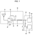
- Fig. 1 is a block diagram illustrating the connection relationship between a load-connection-state detection circuit 100 and a load circuit 50 according to the embodiment of the present invention.
- the load-connection-state detection circuit 100 is included in a GPS receiver 150 mounted in a vehicle or the like.
- the GPS receiver 150 includes a GPS receiving circuit 120 as well as the load-connection-state detection circuit 100, and performs various types of processing for GPS reception.
- the load-connection-state detection circuit 100 connected to a power terminal 22 supplies power to the load circuit 50.
- a high-frequency-signal input terminal 121 of the GPS receiving circuit 120 is connected to a connector 21 of the load-connection-state detection circuit 100, and the high-frequency-signal input terminal 121 receives a high frequency signal from the load circuit 50.
- a capacitor 122 for cutting a direct current is connected between the connector 21 and the high-frequency-signal input terminal 121.
- the load circuit 50 includes an antenna 51, an amplifying circuit 52, an inductor 53, a capacitor 54, a high-frequency-signal output terminal 55, and a cable 56.
- the cable 56 which connects the GPS receiver 150 to the amplifying circuit 52 plays a role of supplying power from the load-connection-state detection circuit 100 to the amplifying circuit 52, as well as of transmitting a high frequency signal received at the antenna 51 to the GPS receiver 150.
- the antenna 51 receives an incoming GPS signal and transmits it to the amplifying circuit 52.
- the amplifying circuit 52 amplifies the received GPS signal which is transmitted from the high-frequency-signal output terminal 55 via the cable 56 to the high-frequency-signal input terminal 121 of the GPS receiving circuit 120.
- a power terminal in the amplifying circuit 52 is connected to the cable 56 via the inductor 53 so that a high frequency signal which is output from the amplifying circuit 52 is not affected.
- An output terminal of the amplifying circuit 52 for a high frequency signal is connected to the cable 56 via the capacitor 54 so that a direct current does not flow from the load-connection-state detection circuit 100.
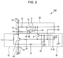
- Fig. 2 is a circuit diagram of the load-connection-state detection circuit 100 according to the embodiment of the present invention. As illustrated in Fig. 2 , the load-connection-state detection circuit 100 is constituted by a current limiting circuit 10, a load-connection-state determination circuit 20, and a switching circuit 30.
- the current limiting circuit 10 includes a first transistor 1 and a second transistor 2.
- the current limiting circuit 10 also includes a first resistance 11, a sixth resistance 16, a seventh resistance 17, and an eighth resistance 18 to connect between the transistors or between each transistor and the power terminal 22 or the connector 21.
- the load circuit 50 is connected to the connector 21.
- the power terminal 22 is supplied with a power supply voltage Vcc obtained, for example, by lowering the voltage of a battery (not illustrated) of a vehicle through a regulator (not illustrated), from the outside.
- the load-connection-state detection circuit 100 according to the embodiment of the present invention has a Vcc of 5 V.
- the first transistor 1 is a PNP bipolar transistor.
- the emitter of the first transistor 1 is connected to the power terminal 22 via a second resistance 12, and the collector is connected to the connector 21.
- the first resistance 11 is connected between the emitter and the collector of the first transistor 1.
- the current limiting circuit 10 causes a current to flow through the first resistance 11.
- the resistance value of the first resistance 11 may be, for example, 10 k ⁇ .
- the second transistor 2 which is an NPN bipolar transistor has a base connected to one end of the eighth resistance 18 in which the other end is connected to the ground, and a collector connected to the base of the first transistor 1 via the sixth resistance 16. The base of the second transistor 2 is connected to the collector of the first transistor 1 through the seventh resistance 17.
- the load-connection-state determination circuit 20 is capable of detecting the state of the load circuit 50 connected to the connector 21. Specifically, the load-connection-state determination circuit 20 includes the second resistance 12, a comparator 4, a third resistance 13, a fourth resistance 14, and a fifth resistance 15. The load-connection-state determination circuit 20 is provided with a first output terminal 41 and a second output terminal 42 for determining the load connection state.
- one end of the second resistance 12 is connected to the power terminal 22, and the other end is connected to the emitter of the first transistor 1.
- An inverting input terminal 4a (-) of the comparator 4 is connected to one end of the second resistance 12 via the third resistance 13, and a non-inverting input terminal 4b (+) is connected to the other end of the second resistance 12 via the fourth resistance 14.
- the fifth resistance 15 functioning as a feedback resistor is connected between the inverting input terminal 4a (-) and a comparator output terminal 4c.
- the first output terminal 41 is connected to the comparator output terminal 4c of the comparator 4, and the second output terminal 42 is connected to the collector of the second transistor 2 in the current limiting circuit 10.
- the second resistance 12 is connected between the power terminal 22 and the first transistor 1 in a series manner to the first transistor 1.
- the resistance value of the second resistance 12 is set so that a current according to the connection state of the load circuit 50 flows.
- the load-connection-state determination circuit 20 is capable of detecting a current flowing through the second resistance 12.
- the second resistance 12 has a predetermined resistance value for enabling the comparator 4 to detect the state of the load circuit 50 connected to the connector 21. For example, in the case where the impedance of the load circuit 50 is in a range of 100 ⁇ to 5 k ⁇ in the normal connection state, the resistance value of the second resistance 12 may be set to 4.7 ⁇ .
- the third resistance 13, the fourth resistance 14, and the fifth resistance 15 are resistances for adjusting the gain of the load-connection-state determination circuit 20.
- the resistance value of the third resistance 13 and the fourth resistance 14 may be set, for example, to 47 ⁇ , and the resistance value of the fifth resistance 15 may be set, for example, to 15 k ⁇ .
- the impedance of the load circuit 50 is smaller than a threshold which is the upper limit of the appropriate range (for example, value smaller than 5 k ⁇ )
- a current flowing through the second resistance 12 is made larger than a predetermined value. Therefore, the potential difference between the inverting input terminal 4a (-) and the non-inverting input terminal 4b (+) of the comparator 4 is made larger than a predetermined value.
- the comparator output terminal 4c of the comparator 4 that is, the first output terminal 41 has a low potential (hereinafter, referred to as a low level).
- the impedance of the load circuit 50 is larger than a threshold (for example, a value larger than 5 k ⁇ )
- a threshold for example, a value larger than 5 k ⁇
- the comparator 4 does not operate, and the comparator output terminal 4c of the comparator 4, that is, the first output terminal 41 is supplied with a high potential (hereinafter, referred to as a high level).
- the switching circuit 30 includes a field effect transistor 3a (hereinafter, referred to as a FET 3a) serving as a switching element 3.
- the gate of the FET 3a serving as a control terminal of the switching element 3 is connected to the collector of the second transistor 2, and the drain of the FET 3a serving as one end of the switching element 3 is connected to the base of the second transistor 2.
- the source of the FET 3a serving as the other end of the switching element 3 is connected to the ground.
- the load-connection-state detection circuit 100 uses the field effect transistor 3a serving as the switching element 3, enabling the switching operation to be easily performed.
- the circuit operation of the load-connection-state detection circuit 100 will be described by using Figs. 2 and 3 .
- the circuit operation of the load-connection-state detection circuit 100 at the time when normal current limiting is performed in a state in which an abnormal voltage is not applied from the outside to the connector 21 is different from one at the time when an abnormal voltage which is higher than the power supply voltage Vcc is applied from the outside in a state in which the load circuit 50 is not connected to the connector 21.
- the state in which the current limiting is performed and the state in which an abnormal voltage is applied will be separately described.
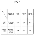
- Fig. 3 illustrates a table describing the operation states of elements by classifying the impedance states of the load circuit 50 into modes, i.e., an appropriate impedance mode, a high impedance mode, and a low impedance mode.
- the operation states of elements in each mode are the on or off states of the first transistor 1, the second transistor 2, and the FET 3a. Whether the voltages of the output terminals, i.e., the first output terminal 41 and the second output terminal 42, are in the low level or in the high level is also described.
- the high-level voltage is one which causes the first transistor 1, the second the transistor 2, or the FET 3a to turn on when the voltage is applied to each of the bases of the transistors or the gate of the FET.
- the low-level voltage is one which causes the first transistor 1, the second transistor 2, or the FET 3a to turn off when the voltage is applied to each of the bases of the transistors or the gate of the FET.
- the minimum and maximum values of the appropriate impedance of the load circuit 50 are set to predetermined values.
- the minimum value of the appropriate impedance of the load circuit 50 is set to 100 ⁇
- the maximum value of the appropriate impedance is set to 5 k ⁇ .
- the impedance of the load circuit 50 which is equal to or larger than 100 ⁇ and equal to or smaller than 5 k ⁇ refers to as the appropriate impedance; the impedance smaller than 100 ⁇ , the low impedance; and the impedance larger than 5 k ⁇ , the high impedance.
- the power supply voltage Vcc is applied from the power terminal 22 via the second resistance 12 and the first resistance 11 to the connector 21, and a current flows through the load circuit 50.
- the impedance of the load circuit 50 is the appropriate impedance, the potential difference between the inverting input terminal 4a (-) and the non-inverting input terminal 4b (+) of the comparator 4 is larger than the predetermined value, resulting in the state in which the comparator output terminal 4c of the comparator 4 is in the low level. Therefore, the emitter of the second transistor 2 is in the low level.
- a voltage is applied to the base of the second transistor 2 via the second resistance 12, the first resistance 11, and the seventh resistance 17. Therefore, the second transistor 2 is turned on.
- the second transistor 2 Since the second transistor 2 turns on, the base of the first transistor 1 is in the low level. Therefore, the first transistor 1 is turned on. At that time, since the gate of the FET 3a is also in the low level, the FET 3a is turned off. The levels of the first output terminal 41 and the second output terminal 42 at that time are in the low level.
- the first transistor 1 turns on, and the power is therefore supplied from the power terminal 22 via the first transistor 1 to the load circuit 50.
- the circuit operation states of the load-connection-state detection circuit 100 in the first mode will be described in the first mode in Fig. 3 .
- the state of the high impedance includes a state in which the connection state of the load circuit 50 is open.
- the power supply voltage Vcc is applied from the power terminal 22 via the second resistance 12 and the first resistance 11 to the connector 21, and a current flows through the load circuit 50.
- the connection state of the load circuit 50 is open, the power supply voltage Vcc is applied from the power terminal 22 via the second resistance 12 and the first resistance 11 to the connector 21.
- the impedance of the load circuit 50 is the high impedance, the potential difference between the inverting input terminal 4a (-) and the non-inverting input terminal 4b (+) of the comparator 4 is smaller than the predetermined value, and the comparator 4 therefore does not operate, resulting in the state in which the comparator output terminal 4c of the comparator 4 is in the high level.
- the emitter of the second transistor 2 is in the high level. Accordingly, the second transistor 2 is turned off. Since the second transistor 2 turns off, the base of the first transistor 1 is in the high level, and the first transistor 1 is also turned off. At that time, since the gate of the FET 3a is also in the high level, the FET 3a turns.on. The levels of the first output terminal 41 and the second output terminal 42 at that time are in the high level.
- the first transistor 1 turns off, causing the power not to be supplied from the power terminal 22 via the first transistor 1 to the load circuit 50.
- Circuit operation states of the load-connection-state detection circuit 100 in the second mode will be described in the second mode in Fig. 3 .
- the state of the low impedance includes a state in which the connection state of the load circuit 50 is shorted out to the ground.
- the power supply voltage Vcc is applied from the power terminal 22 via the second resistance 12 and the first resistance 11 to the connector 21, and a current flows through the load circuit 50.
- the impedance of the load circuit 50 is the low impedance
- the potential difference between the inverting input terminal 4a (-) and the non-inverting input terminal 4b (+) of the comparator 4 is larger than the predetermined value, resulting in the state in which the comparator output terminal 4c of the comparator 4 is in the low level. Therefore, the emitter of the second transistor 2 is in the low level.
- a voltage obtained by dividing the voltage by using the combined resistance of the second resistance 12 and the first resistance 11 and by using the impedance of the load circuit 50 is applied to the base of the second transistor 2.
- the voltage of the base of the second transistor 2 is not one which causes the second transistor 2 to turn on.
- the thresholds for the impedances of the second resistance 12, the first resistance 11, and the load circuit 50 are determined so that the second transistor 2 is not turned on. Therefore, the second transistor 2 is turned off. Since the second transistor 2 turns off, the base of the first transistor 1 is in the high level, and the first transistor 1 is turned off. At that time, the gate of the FET 3a is in the high level, and the FET 3a therefore turns on. The level of the first output terminal 41 at that time is in the low level, and the level of the second output terminal 42 is in the high level.
- Circuit operation states of the load-connection-state detection circuit 100 in the third mode are described in the third mode in Fig. 3 .
- the load-connection-state detection circuit 100 can limit a current.
- the combinations of the voltage level of the first output terminal 41 and that of the second output terminal 42 are different from each other. Therefore, by checking the voltage levels of the first output terminal 41 at which the output voltage of the comparator 4 appears and the second output terminal 42 at which the voltage of the collector of the second transistor 2 appears, the connection state of the load circuit 50 is easily detected.
- the load-connection-state detection circuit 100 can easily detect a state, such as the cutoff or short-circuit of the cable 56 or a failure of the amplifying circuit 52.
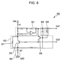
- a circuit operation of the load-connection-state detection circuit 100 performed when an abnormal voltage is applied such as when a voltage higher than the power supply voltage Vcc, for example, a voltage of a battery mounted in a vehicle, is accidentally applied from the outside in a state in which the load circuit 50 is not connected to the connector 21, will be described by using Figs. 2 and 4 .
- the state of the load-connection-state detection circuit 100 in a state in which the load circuit 50 in the appropriate impedance mode is connected to the connector 21 and in which the voltage of the connector 21 is an appropriate voltage will be described for comparison. This case is the same as the circuit operation at the time when the impedance of the load circuit 50 is the appropriate impedance, that is, in the first mode, as described above.
- the first transistor 1 turns on and the second transistor 2 also turns on in the first mode. Since the load circuit 50 has an appropriate impedance, an appropriate voltage is applied to the connector 21 via the second resistance 12 and the first transistor 1. At that time, since the voltage of the collector of the second transistor 2 is in the low level, the voltage of the gate of the FET 3a is also in the low level. Therefore, the FET 3a turns off. Accordingly, the FET 3a does not have an influence on the operation of the first transistor 1 and the second transistor 2.
- a circuit operation of the load-connection-state detection circuit 100 at the time when an abnormal voltage is applied in the case where the load circuit 50 is not connected to the connector 21 and where a voltage higher than the power supply voltage Vcc is applied from the outside (fourth mode) will be described.
- a voltage higher than the power supply voltage Vcc for example, a high voltage such as a battery voltage
- a high voltage such as a battery voltage
- the connector 21 When a voltage higher than the power supply voltage Vcc, for example, a high voltage such as a battery voltage, is applied to the connector 21, a large voltage relative to the emitter of the second transistor 2 is applied to the base of the second transistor 2. Therefore, the second transistor 2 is turned on.
- the high voltage applied to the connector 21 is applied to the emitter of the first transistor 1 via the first resistance 11, and appears at the base of the first transistor 1.
- the voltage is applied to the gate of the FET 3a. Accordingly, the voltage applied to the gate of the FET 3a becomes higher than the gate threshold voltage, the FET 3a is turned on, and the drain of the FET 3a is in the low level.
- the base of the second transistor 2 is in the low level, and the second transistor 2 is turned off. Therefore, the first transistor 1 is also turned off.
- a current caused by the abnormal voltage applied to the connector 21 does not flow through the first transistor 1, and flows through the first resistance 11 connected between the emitter and the collector of the first transistor 1, enabling the current value to be suppressed.
- the semiconductor devices in the circuit can be protected.
- a current flowing through a regulator (not illustrated) connected between the vehicle battery (not illustrated) and the power terminal 22 is also reduced, enabling the semiconductor devices in the regulator to be protected.
- Circuit operation states of the load-connection-state detection circuit 100 in the fourth mode are described in the fourth mode in Fig. 4 .
- the first transistor 1 and the second transistor 2 are turned off, preventing a large current from flowing through the first transistor 1 and the second transistor 2 and preventing the semiconductor devices from being damaged.
- the load-connection-state detection circuit 100 can limit a current and turn off the first transistor 1 and the second transistor 2 when an abnormal voltage higher than the power supply voltage Vcc is applied to the connector 21, by adding one element which is the switching element 3.
- a current caused by an abnormal voltage applied to the connector 21 flows through the first resistance 11 connected between the emitter and the collector of the first transistor 1, enabling the semiconductor devices in the circuit to be protected. Therefore, a load-connection-state detection circuit which protects the semiconductor devices in the circuit even when an abnormal voltage is applied to a connector can be achieved without increasing the circuit size.
- the present invention is not limited to the description in the above-described embodiment, and can be implemented by changing the embodiment as appropriate in such a manner that the effect is achieved.
- the load-connection-state detection circuit in the present invention includes components equivalent to those illustrated in Fig. 2 .
- Other components may be included as long as the operation is not prevented from being performed.
- a bipolar transistor or the like may be used instead of a FET.
Description
- The present invention relates to a load-connection-state detection circuit which is connected to a load circuit and which detects the connection state of the load circuit, and particularly to a load-connection-state detection circuit having a current limiting circuit.
- In receivers used in, for example, global positioning system (GPS) apparatuses mounted in vehicles or the like, it is important that a load circuit is satisfactorily connected to receive incoming radio waves optimally. To detect the connection state of a load circuit, a load-connection-state detection circuit which detects whether or not the connection state of the load circuit is satisfactory may be installed in a receiver. A known load-connection-state detection circuit performs current limiting by turning off a switching element when the impedance of the load circuit is smaller than a predetermined value (for example, see
Japanese Unexamined Patent Application Publication No. 2012-191381 -
Fig. 5 illustrates a load-connection-state detection circuit 900 as a first related art example described inJapanese Unexamined Patent Application Publication No. 2012-191381 - As illustrated in
Fig. 5 , the load-connection-state detection circuit 900 includes anantenna detecting circuit 951, a current limitingcircuit 952, atemperature compensating circuit 953, and apotential holding circuit 954. The load-connection-state detection circuit 900 includes a power terminal A1 supplied with a power supply voltage Vdd, and a connector B1 connected to anantenna 902. The load-connection-state detection circuit 900 also includes a first output terminal Out1 and a second output terminal Out2 for transmitting detection results of the connection state of theantenna 902 to the outside. - In the load-connection-
state detection circuit 900, atransistor 925 and aresistance 921 are connected in parallel to each other. When the impedance of theantenna 902 is equal to or larger than a predetermined value, thetransistor 926 is turned on, and thetransistor 925 is also turned on. In contrast, when the impedance of theantenna 902 is equal to or smaller than the predetermined value, thetransistor 926 is turned off, and thetransistor 925 is also turned off. Therefore, when the impedance of theantenna 902 is smaller than the predetermined value, instead of passing a current through thetransistor 925, a current can flow through theresistance 921. That is, a current flowing through thetransistor 925 can be limited. Accordingly, damage of thetransistor 925 caused by a large current can be prevented. - As described above, when the impedance of the
antenna 902 is smaller than the predetermined value, the load-connection-state detection circuit 900 performs current limiting on thetransistor 925. Therefore, damage of thetransistor 925 caused by a large current can be prevented. However, in a vehicle-mounted circuit such as the load-connection-state detection circuit 900, external power such as a car battery may be accidentally connected to the connector B1 connected to theantenna 902. In such a case, an excessive current flowing from a car battery may cause damage of semiconductor devices in the load-connection-state detection circuit 900 or damage of semiconductor devices in a power supplying circuit (not illustrated) for stabling the voltage of the power from the car battery. - To address such a problem, electronic equipment as described in
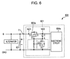
JP 2012-222885 A Electronic equipment 804 as a second related art example described inJP 2012-222885 A Fig. 6 . - In a
protection circuit 801 in theelectronic equipment 804, when a direct-current power supply 821 is satisfactorily connected, that is, when the positive electrode + of the direct-current power supply 821 is connected to a direct-current power supply line B and the negative electrode - of the direct-current power supply 821 is connected to a ground power supply line GND, aP channel FET 803a is turned on. The P channel FET 803a supplies power between a first node ND1 and a second node ND2. Therefore, anelectronic circuit 804a operates normally by using the direct-current power supply 821. - In contrast, when the direct-
current power supply 821 is connected the other way around, that is, when the positive electrode + of the direct-current power supply 821 is connected to the ground power supply line GND and the negative electrode - of the direct-current power supply 821 is connected to the direct-current power supply line B, the P channel FET 803a is turned off. TheP channel FET 803a interrupts power between the first node ND1 and the second node ND2, enabling theelectronic circuit 804a to be protected from the reverse connection. - However, in the
electronic equipment 804, theprotection circuit 801 constituted by multiple elements needs to be disposed between the direct-current power supply line B and theelectronic circuit 804a and between the ground power supply line GND and theelectronic circuit 804a. As a result, the circuit size of theelectronic equipment 804 is increased, and a large number of parts need to form theprotection circuit 801, causing the cost of theelectronic equipment 804 to be increased. - To provide a circuit substituted for the
protection circuit 801 described above, a diode for preventing reverse connection may be disposed between a terminal T1 and theelectronic circuit 804a. In this case, since the number of parts is only one, the circuit size is not increased and the cost of theelectronic equipment 804 is not markedly increased. However, when a diode is disposed between the terminal T1 and theelectronic circuit 804a, the voltage is decreased by the forward voltage of the diode, and a power supply voltage obtained through voltage drop is supplied from the direct-current power supply 821 to theelectronic circuit 804a. As a result, a voltage range used by theelectronic circuit 804a is narrowed, causing the circuit performance of theelectronic circuit 804a to be affected. - In view of these problems of the related art, the present invention providers a load-connection-state detection circuit, as defined in
claim 1, which can perform current limiting and which can protect semiconductor devices in the circuit even when an abnormal voltage higher than a power supply voltage is applied to a connector, without increasing the circuit size. - To solve these problems, there is provided a load-connection-state detection circuit including a power terminal, a connector, and a current limiting circuit. The power terminal is supplied with power from the outside. The connector supplies power to a load circuit connected to the ground. The current limiting circuit includes a PNP first transistor having an emitter connected to the power terminal and having a collector connected to the connector, an NPN second transistor having an emitter connected to the power terminal, having a collector connected to a base of the first transistor, and having a base connected to the collector of the first transistor, and a first resistance connected between the emitter and the collector of the first transistor, in such a manner that a current flows via the first resistance when a current is limited. The load-connection-state detection circuit further includes a switching element having a control end, one end of the switching element is connected to the base of the second transistor, the other end of the switching element is connected to the ground, and the control end is connected to the collector of the second transistor.
- The load-connection-state detection circuit having the above-described configuration can perform current limiting and can turn off the first transistor and the second transistor when an abnormal voltage higher than a power supply voltage is applied to a connector, by adding one switching element. As a result, a current caused by the abnormal voltage applied to the connector flows through the first resistance connected between the emitter and the collector of the first transistor, enabling the semiconductor devices in the circuit to be protected. Therefore, a load-connection-state detection circuit which can protect the semiconductor devices in the circuit even when an abnormal voltage is applied to the connector is achieved without increasing the circuit size.
- In the load-connection-state detection circuit having the above-described configuration, preferably the switching element which is a field effect transistor has a drain connected to the base of the second transistor and also has a source connected to the ground.
- The load-connection-state detection circuit having the above-described configuration uses a field effect transistor as a switching element, enabling the switching operation to be easily performed.
- In the above-described configuration, the load-connection-state detection circuit may further include a second resistance and a comparator. The second resistance has one end connected to the power terminal and has the other end connected to the emitter of the first transistor. The comparator has an inverting input terminal connected to one end of the second resistance via a third resistance and has a non-inverting input terminal connected to the other end of the second resistance via a fourth resistance. A fifth resistance is connected between the inverting input terminal and an output end. A connection state of the load circuit is detected from an output voltage from the comparator and from a voltage of the collector of the second transistor.
- The load-connection-state detection circuit having the above-described configuration can easily detect the connection state of the load circuit connected to the connector by checking the output voltage of the comparator and the voltage of the collector of the second transistor.
- In the load-connection-state detection circuit having the above-described configuration, the load circuit may include a cable and an amplifying circuit.
- The load-connection-state detection circuit having the above-described configuration can easily detect the state, such as the cutoff or short-circuit of the cable connected to the connector or a failure of the amplifying circuit.
- The load-connection-state detection circuit in the present invention can perform current limiting and can turn off the first transistor and the second transistor when an abnormal voltage higher than a power supply voltage is applied to a connector, by adding one switching element. As a result, a current caused by the abnormal voltage applied to the connector flows through the first resistance connected between the emitter and the collector of the first transistor, enabling the semiconductor devices in the circuit to be protected. Therefore, a load-connection-state detection circuit which can protect the semiconductor devices in the circuit even when an abnormal voltage is applied to the connector is achieved without increasing the circuit size.
-
-
Fig. 1 is a block diagram illustrating the connection relationship between a load-connection-state detection circuit and a load circuit according to an embodiment of the present invention; -
Fig. 2 is a circuit diagram of the load-connection-state detection circuit according to an embodiment of the present invention; -
Fig. 3 is a diagram illustrating a table for the load-connection-state detection circuit which describes the states of transistors, a FET, a first output terminal, and a second output terminal at the time when current limiting is performed, according to an embodiment of the present invention; -
Fig. 4 is a diagram illustrating a table for the load-connection-state detection circuit which describes the states of the transistors and the FET at the time when an abnormal voltage higher than a power supply voltage is applied to a connector, according to an embodiment of the present invention; -
Fig. 5 is a circuit diagram of a load-connection-state detection circuit according to a first related art example; and -
Fig. 6 is a circuit diagram of a load-connection-state detection circuit according to a second related art example. - An embodiment of the present invention will be described below with reference to the drawings.
-
Fig. 1 is a block diagram illustrating the connection relationship between a load-connection-state detection circuit 100 and aload circuit 50 according to the embodiment of the present invention. - As illustrated in
Fig. 1 , the load-connection-state detection circuit 100 according to the embodiment of the present invention is included in aGPS receiver 150 mounted in a vehicle or the like. TheGPS receiver 150 includes aGPS receiving circuit 120 as well as the load-connection-state detection circuit 100, and performs various types of processing for GPS reception. The load-connection-state detection circuit 100 connected to apower terminal 22 supplies power to theload circuit 50. A high-frequency-signal input terminal 121 of theGPS receiving circuit 120 is connected to aconnector 21 of the load-connection-state detection circuit 100, and the high-frequency-signal input terminal 121 receives a high frequency signal from theload circuit 50. Acapacitor 122 for cutting a direct current is connected between theconnector 21 and the high-frequency-signal input terminal 121. - As illustrated in
Fig. 1 , theload circuit 50 includes anantenna 51, an amplifyingcircuit 52, aninductor 53, acapacitor 54, a high-frequency-signal output terminal 55, and acable 56. Thecable 56 which connects theGPS receiver 150 to the amplifyingcircuit 52 plays a role of supplying power from the load-connection-state detection circuit 100 to the amplifyingcircuit 52, as well as of transmitting a high frequency signal received at theantenna 51 to theGPS receiver 150. Theantenna 51 receives an incoming GPS signal and transmits it to the amplifyingcircuit 52. The amplifyingcircuit 52 amplifies the received GPS signal which is transmitted from the high-frequency-signal output terminal 55 via thecable 56 to the high-frequency-signal input terminal 121 of theGPS receiving circuit 120. A power terminal in the amplifyingcircuit 52 is connected to thecable 56 via theinductor 53 so that a high frequency signal which is output from the amplifyingcircuit 52 is not affected. An output terminal of the amplifyingcircuit 52 for a high frequency signal is connected to thecable 56 via thecapacitor 54 so that a direct current does not flow from the load-connection-state detection circuit 100. - The circuit configuration of the load-connection-
state detection circuit 100 will be described.Fig. 2 is a circuit diagram of the load-connection-state detection circuit 100 according to the embodiment of the present invention. As illustrated inFig. 2 , the load-connection-state detection circuit 100 is constituted by a current limitingcircuit 10, a load-connection-state determination circuit 20, and aswitching circuit 30. - The current limiting
circuit 10 includes afirst transistor 1 and asecond transistor 2. The current limitingcircuit 10 also includes a first resistance 11, asixth resistance 16, aseventh resistance 17, and aneighth resistance 18 to connect between the transistors or between each transistor and thepower terminal 22 or theconnector 21. As described above, theload circuit 50 is connected to theconnector 21. Thepower terminal 22 is supplied with a power supply voltage Vcc obtained, for example, by lowering the voltage of a battery (not illustrated) of a vehicle through a regulator (not illustrated), from the outside. The load-connection-state detection circuit 100 according to the embodiment of the present invention has a Vcc of 5 V. - The
first transistor 1 is a PNP bipolar transistor. The emitter of thefirst transistor 1 is connected to thepower terminal 22 via asecond resistance 12, and the collector is connected to theconnector 21. The first resistance 11 is connected between the emitter and the collector of thefirst transistor 1. In the case where thefirst transistor 1 is turned off when current limiting is performed, the current limitingcircuit 10 causes a current to flow through the first resistance 11. The resistance value of the first resistance 11 may be, for example, 10 kΩ. - The
second transistor 2 which is an NPN bipolar transistor has a base connected to one end of theeighth resistance 18 in which the other end is connected to the ground, and a collector connected to the base of thefirst transistor 1 via thesixth resistance 16. The base of thesecond transistor 2 is connected to the collector of thefirst transistor 1 through theseventh resistance 17. - The load-connection-
state determination circuit 20 is capable of detecting the state of theload circuit 50 connected to theconnector 21. Specifically, the load-connection-state determination circuit 20 includes thesecond resistance 12, acomparator 4, athird resistance 13, afourth resistance 14, and afifth resistance 15. The load-connection-state determination circuit 20 is provided with afirst output terminal 41 and asecond output terminal 42 for determining the load connection state. - In the load-connection-
state determination circuit 20, one end of thesecond resistance 12 is connected to thepower terminal 22, and the other end is connected to the emitter of thefirst transistor 1. An invertinginput terminal 4a (-) of thecomparator 4 is connected to one end of thesecond resistance 12 via thethird resistance 13, and anon-inverting input terminal 4b (+) is connected to the other end of thesecond resistance 12 via thefourth resistance 14. Thefifth resistance 15 functioning as a feedback resistor is connected between the invertinginput terminal 4a (-) and acomparator output terminal 4c. Thefirst output terminal 41 is connected to thecomparator output terminal 4c of thecomparator 4, and thesecond output terminal 42 is connected to the collector of thesecond transistor 2 in the current limitingcircuit 10. - The
second resistance 12 is connected between thepower terminal 22 and thefirst transistor 1 in a series manner to thefirst transistor 1. The resistance value of thesecond resistance 12 is set so that a current according to the connection state of theload circuit 50 flows. The load-connection-state determination circuit 20 is capable of detecting a current flowing through thesecond resistance 12. Thesecond resistance 12 has a predetermined resistance value for enabling thecomparator 4 to detect the state of theload circuit 50 connected to theconnector 21. For example, in the case where the impedance of theload circuit 50 is in a range of 100 Ω to 5 kΩ in the normal connection state, the resistance value of thesecond resistance 12 may be set to 4.7 Ω. - The
third resistance 13, thefourth resistance 14, and thefifth resistance 15 are resistances for adjusting the gain of the load-connection-state determination circuit 20. The resistance value of thethird resistance 13 and thefourth resistance 14 may be set, for example, to 47 Ω, and the resistance value of thefifth resistance 15 may be set, for example, to 15 kΩ. - In the load-connection-
state determination circuit 20 having such a configuration, when the impedance of theload circuit 50 is smaller than a threshold which is the upper limit of the appropriate range (for example, value smaller than 5 kΩ), a current flowing through thesecond resistance 12 is made larger than a predetermined value. Therefore, the potential difference between the invertinginput terminal 4a (-) and thenon-inverting input terminal 4b (+) of thecomparator 4 is made larger than a predetermined value. As a result, thecomparator output terminal 4c of thecomparator 4, that is, thefirst output terminal 41 has a low potential (hereinafter, referred to as a low level). - When the impedance of the
load circuit 50 is larger than a threshold (for example, a value larger than 5 kΩ), the value of a current flowing through thesecond resistance 12 is smaller than a predetermined value, resulting in the state in which a potential difference between the invertinginput terminal 4a (-) and thenon-inverting input terminal 4b (+) of thecomparator 4 is smaller than the predetermined value. In this case, thecomparator 4 does not operate, and thecomparator output terminal 4c of thecomparator 4, that is, thefirst output terminal 41 is supplied with a high potential (hereinafter, referred to as a high level). - The switching
circuit 30 includes afield effect transistor 3a (hereinafter, referred to as aFET 3a) serving as a switching element 3. The gate of theFET 3a serving as a control terminal of the switching element 3 is connected to the collector of thesecond transistor 2, and the drain of theFET 3a serving as one end of the switching element 3 is connected to the base of thesecond transistor 2. The source of theFET 3a serving as the other end of the switching element 3 is connected to the ground. - When the gate-source voltage of the
FET 3a is equal to or larger than a threshold voltage and when the voltage is sufficiently large, theFET 3a turns on. When the gate-source voltage of theFET 3a is smaller than a threshold voltage which is a sufficiently small voltage, theFET 3a turns off. Thus, the load-connection-state detection circuit 100 uses thefield effect transistor 3a serving as the switching element 3, enabling the switching operation to be easily performed. - The circuit operation of the load-connection-
state detection circuit 100 will be described by usingFigs. 2 and3 . The circuit operation of the load-connection-state detection circuit 100 at the time when normal current limiting is performed in a state in which an abnormal voltage is not applied from the outside to theconnector 21 is different from one at the time when an abnormal voltage which is higher than the power supply voltage Vcc is applied from the outside in a state in which theload circuit 50 is not connected to theconnector 21. Thus, the state in which the current limiting is performed and the state in which an abnormal voltage is applied will be separately described. - A circuit operation in current limiting will be described.
Fig. 3 illustrates a table describing the operation states of elements by classifying the impedance states of theload circuit 50 into modes, i.e., an appropriate impedance mode, a high impedance mode, and a low impedance mode. The operation states of elements in each mode are the on or off states of thefirst transistor 1, thesecond transistor 2, and theFET 3a. Whether the voltages of the output terminals, i.e., thefirst output terminal 41 and thesecond output terminal 42, are in the low level or in the high level is also described. The high-level voltage is one which causes thefirst transistor 1, the second thetransistor 2, or theFET 3a to turn on when the voltage is applied to each of the bases of the transistors or the gate of the FET. The low-level voltage is one which causes thefirst transistor 1, thesecond transistor 2, or theFET 3a to turn off when the voltage is applied to each of the bases of the transistors or the gate of the FET. - In the load-connection-
state detection circuit 100, the minimum and maximum values of the appropriate impedance of theload circuit 50 are set to predetermined values. According to the embodiment, the minimum value of the appropriate impedance of theload circuit 50 is set to 100 Ω, whereas the maximum value of the appropriate impedance is set to 5 kΩ. Hereinafter, the impedance of theload circuit 50 which is equal to or larger than 100 Ω and equal to or smaller than 5 kΩ refers to as the appropriate impedance; the impedance smaller than 100 Ω, the low impedance; and the impedance larger than 5 kΩ, the high impedance. - A circuit operation performed when the impedance of the
load circuit 50 is the appropriate impedance, that is, in a first mode, will be described. - In the first mode, the power supply voltage Vcc is applied from the
power terminal 22 via thesecond resistance 12 and the first resistance 11 to theconnector 21, and a current flows through theload circuit 50. As described above, when the impedance of theload circuit 50 is the appropriate impedance, the potential difference between the invertinginput terminal 4a (-) and thenon-inverting input terminal 4b (+) of thecomparator 4 is larger than the predetermined value, resulting in the state in which thecomparator output terminal 4c of thecomparator 4 is in the low level. Therefore, the emitter of thesecond transistor 2 is in the low level. A voltage is applied to the base of thesecond transistor 2 via thesecond resistance 12, the first resistance 11, and theseventh resistance 17. Therefore, thesecond transistor 2 is turned on. Since thesecond transistor 2 turns on, the base of thefirst transistor 1 is in the low level. Therefore, thefirst transistor 1 is turned on. At that time, since the gate of theFET 3a is also in the low level, theFET 3a is turned off. The levels of thefirst output terminal 41 and thesecond output terminal 42 at that time are in the low level. - As a result, in the first mode in which the impedance of the
load circuit 50 is the appropriate impedance, thefirst transistor 1 turns on, and the power is therefore supplied from thepower terminal 22 via thefirst transistor 1 to theload circuit 50. The circuit operation states of the load-connection-state detection circuit 100 in the first mode will be described in the first mode inFig. 3 . - A circuit operation performed when the impedance of the
load circuit 50 is the high impedance, that is, in a second mode will be described. The state of the high impedance includes a state in which the connection state of theload circuit 50 is open. - In the second mode, the power supply voltage Vcc is applied from the
power terminal 22 via thesecond resistance 12 and the first resistance 11 to theconnector 21, and a current flows through theload circuit 50. When the connection state of theload circuit 50 is open, the power supply voltage Vcc is applied from thepower terminal 22 via thesecond resistance 12 and the first resistance 11 to theconnector 21. As described above, when the impedance of theload circuit 50 is the high impedance, the potential difference between the invertinginput terminal 4a (-) and thenon-inverting input terminal 4b (+) of thecomparator 4 is smaller than the predetermined value, and thecomparator 4 therefore does not operate, resulting in the state in which thecomparator output terminal 4c of thecomparator 4 is in the high level. Therefore, the emitter of thesecond transistor 2 is in the high level. Accordingly, thesecond transistor 2 is turned off. Since thesecond transistor 2 turns off, the base of thefirst transistor 1 is in the high level, and thefirst transistor 1 is also turned off. At that time, since the gate of theFET 3a is also in the high level, theFET 3a turns.on. The levels of thefirst output terminal 41 and thesecond output terminal 42 at that time are in the high level. - As a result, in the second mode in which the impedance of the
load circuit 50 is the high impedance, thefirst transistor 1 turns off, causing the power not to be supplied from thepower terminal 22 via thefirst transistor 1 to theload circuit 50. - Circuit operation states of the load-connection-
state detection circuit 100 in the second mode will be described in the second mode inFig. 3 . - A circuit operation performed when the impedance of the
load circuit 50 is the low impedance, that is, in a third mode, will be described. The state of the low impedance includes a state in which the connection state of theload circuit 50 is shorted out to the ground. - In the third mode, the power supply voltage Vcc is applied from the
power terminal 22 via thesecond resistance 12 and the first resistance 11 to theconnector 21, and a current flows through theload circuit 50. As described above, when the impedance of theload circuit 50 is the low impedance, the potential difference between the invertinginput terminal 4a (-) and thenon-inverting input terminal 4b (+) of thecomparator 4 is larger than the predetermined value, resulting in the state in which thecomparator output terminal 4c of thecomparator 4 is in the low level. Therefore, the emitter of thesecond transistor 2 is in the low level. A voltage obtained by dividing the voltage by using the combined resistance of thesecond resistance 12 and the first resistance 11 and by using the impedance of theload circuit 50 is applied to the base of thesecond transistor 2. Since the impedance of theload circuit 50 is the low impedance, the voltage of the base of thesecond transistor 2 is not one which causes thesecond transistor 2 to turn on. In other words, when the impedance of theload circuit 50 is the low impedance, the thresholds for the impedances of thesecond resistance 12, the first resistance 11, and theload circuit 50 are determined so that thesecond transistor 2 is not turned on. Therefore, thesecond transistor 2 is turned off. Since thesecond transistor 2 turns off, the base of thefirst transistor 1 is in the high level, and thefirst transistor 1 is turned off. At that time, the gate of theFET 3a is in the high level, and theFET 3a therefore turns on. The level of thefirst output terminal 41 at that time is in the low level, and the level of thesecond output terminal 42 is in the high level. - Circuit operation states of the load-connection-
state detection circuit 100 in the third mode are described in the third mode inFig. 3 . - As a result, in the third mode in which the impedance of the
load circuit 50 is the low impedance, thefirst transistor 1 turns off, and the power is not supplied from thepower terminal 22 via thefirst transistor 1 to theload circuit 50, whereby a current flows through theload circuit 50 via the first resistance 11. Therefore, when the impedance of theload circuit 50 is the low impedance, a large current does not flow through the semiconductor devices including thefirst transistor 1 even in the case where theload circuit 50 is shorted out to the ground, preventing the semiconductor devices from being damaged. Thus, the load-connection-state detection circuit 100 can limit a current. - States of the
first output terminal 41 and thesecond output terminal 42 for transmitting the result obtained by detecting the connection state of theload circuit 50 to the outside are described in the table inFig. 3 . According to the table, when the impedance of theload circuit 50 is the appropriate impedance, thefirst output terminal 41 is in the low level, and thesecond output terminal 42 is also in the low level. When the impedance of theload circuit 50 is the high impedance, thefirst output terminal 41 is in the high level, and thesecond output terminal 42 is also in the high level. When the impedance of theload circuit 50 is the low impedance, thefirst output terminal 41 is in the low level, and thesecond output terminal 42 is in the high level. Therefore, in the first, second, and third modes, the combinations of the voltage level of thefirst output terminal 41 and that of thesecond output terminal 42 are different from each other. Therefore, by checking the voltage levels of thefirst output terminal 41 at which the output voltage of thecomparator 4 appears and thesecond output terminal 42 at which the voltage of the collector of thesecond transistor 2 appears, the connection state of theload circuit 50 is easily detected. - For example, as illustrated in
Fig. 1 , thecable 56 and the amplifyingcircuit 52 serving as theload circuit 50 are connected to the load-connection-state detection circuit 100. Therefore, the load-connection-state detection circuit 100 can easily detect a state, such as the cutoff or short-circuit of thecable 56 or a failure of the amplifyingcircuit 52. - A circuit operation of the load-connection-
state detection circuit 100 performed when an abnormal voltage is applied, such as when a voltage higher than the power supply voltage Vcc, for example, a voltage of a battery mounted in a vehicle, is accidentally applied from the outside in a state in which theload circuit 50 is not connected to theconnector 21, will be described by usingFigs. 2 and4 . - Before the description about when an abnormal voltage is applied, the state of the load-connection-
state detection circuit 100 in a state in which theload circuit 50 in the appropriate impedance mode is connected to theconnector 21 and in which the voltage of theconnector 21 is an appropriate voltage will be described for comparison. This case is the same as the circuit operation at the time when the impedance of theload circuit 50 is the appropriate impedance, that is, in the first mode, as described above. - As illustrated in the first mode in the table in
Fig. 4 , as described above, thefirst transistor 1 turns on and thesecond transistor 2 also turns on in the first mode. Since theload circuit 50 has an appropriate impedance, an appropriate voltage is applied to theconnector 21 via thesecond resistance 12 and thefirst transistor 1. At that time, since the voltage of the collector of thesecond transistor 2 is in the low level, the voltage of the gate of theFET 3a is also in the low level. Therefore, theFET 3a turns off. Accordingly, theFET 3a does not have an influence on the operation of thefirst transistor 1 and thesecond transistor 2. - A circuit operation of the load-connection-
state detection circuit 100 at the time when an abnormal voltage is applied in the case where theload circuit 50 is not connected to theconnector 21 and where a voltage higher than the power supply voltage Vcc is applied from the outside (fourth mode) will be described. - When a voltage higher than the power supply voltage Vcc, for example, a high voltage such as a battery voltage, is applied to the
connector 21, a large voltage relative to the emitter of thesecond transistor 2 is applied to the base of thesecond transistor 2. Therefore, thesecond transistor 2 is turned on. At the same time, the high voltage applied to theconnector 21 is applied to the emitter of thefirst transistor 1 via the first resistance 11, and appears at the base of thefirst transistor 1. As a result, the voltage is applied to the gate of theFET 3a. Accordingly, the voltage applied to the gate of theFET 3a becomes higher than the gate threshold voltage, theFET 3a is turned on, and the drain of theFET 3a is in the low level. As a result, the base of thesecond transistor 2 is in the low level, and thesecond transistor 2 is turned off. Therefore, thefirst transistor 1 is also turned off. After that, a current caused by the abnormal voltage applied to theconnector 21 does not flow through thefirst transistor 1, and flows through the first resistance 11 connected between the emitter and the collector of thefirst transistor 1, enabling the current value to be suppressed. As a result, the semiconductor devices in the circuit can be protected. A current flowing through a regulator (not illustrated) connected between the vehicle battery (not illustrated) and thepower terminal 22 is also reduced, enabling the semiconductor devices in the regulator to be protected. - Circuit operation states of the load-connection-
state detection circuit 100 in the fourth mode are described in the fourth mode inFig. 4 . - As a result, in the case where a voltage higher than the power supply voltage Vcc is applied to the
connector 21 from the outside, thefirst transistor 1 and thesecond transistor 2 are turned off, preventing a large current from flowing through thefirst transistor 1 and thesecond transistor 2 and preventing the semiconductor devices from being damaged. - As described above, the load-connection-
state detection circuit 100 according to the embodiment of the present invention can limit a current and turn off thefirst transistor 1 and thesecond transistor 2 when an abnormal voltage higher than the power supply voltage Vcc is applied to theconnector 21, by adding one element which is the switching element 3. As a result, a current caused by an abnormal voltage applied to theconnector 21 flows through the first resistance 11 connected between the emitter and the collector of thefirst transistor 1, enabling the semiconductor devices in the circuit to be protected. Therefore, a load-connection-state detection circuit which protects the semiconductor devices in the circuit even when an abnormal voltage is applied to a connector can be achieved without increasing the circuit size. - The present invention is not limited to the description in the above-described embodiment, and can be implemented by changing the embodiment as appropriate in such a manner that the effect is achieved. For example, the load-connection-state detection circuit in the present invention includes components equivalent to those illustrated in
Fig. 2 . Other components may be included as long as the operation is not prevented from being performed. As a switching element, a bipolar transistor or the like may be used instead of a FET.
Claims (4)
- A load-connection-state detection circuit (100) comprising:a power terminal (22) that is supplied with power from the outside;a connector (21) that supplies power to a load circuit (50) connected to the ground; anda current limiting circuit (10),wherein the current limiting circuit (10) includes a PNP first transistor (1) having an emitter coupled to the power terminal (22) and having a collector connected to the connector (21), an NPN second transistor (2) having an emitter coupled to the power terminal (22), having a collector coupled to a base of the first transistor (1), and having a base coupled to the collector of the first transistor (1), and a first resistance (11) connected between the emitter and the collector of the first transistor (1), in such a manner that a current flows via the first resistance (11) when a current is limited,characterized in that the load-connection-state detection circuit (100) further includes a switching element (3) having a control end, one end of the switching element (3) is connected to the base of the second transistor (2), the other end of the switching element (3) is connected to the ground, and the control end is connected to the collector of the second transistor (2).
- The load-connection-state detection circuit (100) according to Claim 1,
wherein the switching element (3) which is a field effect transistor (3a) has a drain connected to the base of the second transistor (2) and also has a source connected to the ground. - The load-connection-state detection circuit (100) according to Claim 1 or 2, further comprising:a second resistance (12) having one end connected to the power terminal (22) and having the other end connected to the emitter of the first transistor (1); anda comparator (4) having an output end, an inverting input terminal connected to one end of the second resistance (12) via a third resistance (13), and having a non-inverting input terminal connected to the other end of the second resistance (12) via a fourth resistance (14), wherein a fifth resistance (15) is connected between the inverting input terminal and the output end, and wherein the output end is connected to the emitter of the second transistor (2),wherein a connection state of the load circuit (50) is detected from an output voltage from the comparator (4) and from a voltage of the collector of the second transistor (2).
- The load-connection-state detection circuit (100) according to any one of Claims 1 to 3,
wherein the load circuit (50) includes a cable and an amplifying circuit.
Applications Claiming Priority (1)
| Application Number | Priority Date | Filing Date | Title |
|---|---|---|---|
| JP2013109780A JP6004487B2 (en) | 2013-05-24 | 2013-05-24 | Load connection status detection circuit |
Publications (2)
| Publication Number | Publication Date |
|---|---|
| EP2806569A1 EP2806569A1 (en) | 2014-11-26 |
| EP2806569B1 true EP2806569B1 (en) | 2016-04-27 |
Family
ID=50828696
Family Applications (1)
| Application Number | Title | Priority Date | Filing Date |
|---|---|---|---|
| EP14168558.6A Not-in-force EP2806569B1 (en) | 2013-05-24 | 2014-05-16 | Load-connection-state detection circuit |
Country Status (2)
| Country | Link |
|---|---|
| EP (1) | EP2806569B1 (en) |
| JP (1) | JP6004487B2 (en) |
Family Cites Families (5)
| Publication number | Priority date | Publication date | Assignee | Title |
|---|---|---|---|---|
| JP2002232333A (en) * | 2001-01-30 | 2002-08-16 | Kenwood Corp | Diversity reception circuit in mobile communication |
| JP2010010755A (en) * | 2008-06-24 | 2010-01-14 | Maspro Denkoh Corp | Television broadcast signal transmission system, power supply unit and signal processing apparatus |
| JP5378737B2 (en) * | 2008-09-24 | 2013-12-25 | 富士通テン株式会社 | Load connection detection circuit, power supply circuit, and electronic equipment |
| JP5638428B2 (en) * | 2011-03-10 | 2014-12-10 | アルプス電気株式会社 | Antenna connection state detection circuit |
| JP2012222885A (en) * | 2011-04-05 | 2012-11-12 | Honda Motor Co Ltd | Protection circuit |
-
2013
- 2013-05-24 JP JP2013109780A patent/JP6004487B2/en not_active Expired - Fee Related
-
2014
- 2014-05-16 EP EP14168558.6A patent/EP2806569B1/en not_active Not-in-force
Also Published As
| Publication number | Publication date |
|---|---|
| EP2806569A1 (en) | 2014-11-26 |
| JP2014230193A (en) | 2014-12-08 |
| JP6004487B2 (en) | 2016-10-12 |
Similar Documents
| Publication | Publication Date | Title |
|---|---|---|
| US8154345B2 (en) | Apparatus and method for current sensing using a wire bond | |
| US9088256B2 (en) | Apparatus and methods for amplifier fault protection | |
| CN106484017B (en) | Semiconductor integrated circuit for voltage stabilizer | |
| US8644777B2 (en) | System and method for power amplifier over-voltage protection | |
| US9325168B2 (en) | Semiconductor device | |
| US9945895B2 (en) | Antenna checking circuit | |
| US10263571B2 (en) | Protection circuit for an RF power amplifier | |
| US10608429B2 (en) | Electro-static discharge protection circuit | |
| CN110192315B (en) | Electronic circuit for providing protection for power supply of receiving device | |
| US10505361B2 (en) | Integrated circuit with reverse current protection and power source disconnection detection | |
| KR101806947B1 (en) | Active circuit | |
| EP2806569B1 (en) | Load-connection-state detection circuit | |
| US8901918B2 (en) | Load connection state detection circuit | |
| US20210234523A1 (en) | Power amplifier circuit | |
| JP5638428B2 (en) | Antenna connection state detection circuit | |
| US20060209477A1 (en) | Input protection circuit | |
| EP2775628B1 (en) | Antenna-apparatus connection circuit | |
| US11196248B2 (en) | Bidirectional flat clamp device with shared voltage sensor circuit | |
| US20070021061A1 (en) | Current detector with variable output voltage level | |
| CN217388208U (en) | Detection control circuit and vehicle | |
| US11296490B2 (en) | Ground fault control for multiple ground paths | |
| US10291020B2 (en) | Overvoltage protection device | |
| JP6538369B2 (en) | Semiconductor device | |
| CN113994560A (en) | Semiconductor circuit for mounting on vehicle and semiconductor circuit |
Legal Events
| Date | Code | Title | Description |
|---|---|---|---|
| PUAI | Public reference made under article 153(3) epc to a published international application that has entered the european phase |
Free format text: ORIGINAL CODE: 0009012 |
|
| 17P | Request for examination filed |
Effective date: 20140516 |
|
| AK | Designated contracting states |
Kind code of ref document: A1 Designated state(s): AL AT BE BG CH CY CZ DE DK EE ES FI FR GB GR HR HU IE IS IT LI LT LU LV MC MK MT NL NO PL PT RO RS SE SI SK SM TR |
|
| AX | Request for extension of the european patent |
Extension state: BA ME |
|
| R17P | Request for examination filed (corrected) |
Effective date: 20150427 |
|
| RBV | Designated contracting states (corrected) |
Designated state(s): AL AT BE BG CH CY CZ DE DK EE ES FI FR GB GR HR HU IE IS IT LI LT LU LV MC MK MT NL NO PL PT RO RS SE SI SK SM TR |
|
| GRAP | Despatch of communication of intention to grant a patent |
Free format text: ORIGINAL CODE: EPIDOSNIGR1 |
|
| RIC1 | Information provided on ipc code assigned before grant |
Ipc: G01R 31/02 20060101ALI20151203BHEP Ipc: H04B 1/18 20060101AFI20151203BHEP Ipc: G01R 31/04 20060101ALI20151203BHEP |
|
| INTG | Intention to grant announced |
Effective date: 20160107 |
|
| RIN1 | Information on inventor provided before grant (corrected) |
Inventor name: MARUYAMA, TAKASHI |
|
| GRAS | Grant fee paid |
Free format text: ORIGINAL CODE: EPIDOSNIGR3 |
|
| GRAA | (expected) grant |
Free format text: ORIGINAL CODE: 0009210 |
|
| AK | Designated contracting states |
Kind code of ref document: B1 Designated state(s): AL AT BE BG CH CY CZ DE DK EE ES FI FR GB GR HR HU IE IS IT LI LT LU LV MC MK MT NL NO PL PT RO RS SE SI SK SM TR |
|
| REG | Reference to a national code |
Ref country code: GB Ref legal event code: FG4D |
|
| REG | Reference to a national code |
Ref country code: CH Ref legal event code: EP |
|
| REG | Reference to a national code |
Ref country code: AT Ref legal event code: REF Ref document number: 795784 Country of ref document: AT Kind code of ref document: T Effective date: 20160515 |
|
| REG | Reference to a national code |
Ref country code: IE Ref legal event code: FG4D |
|
| REG | Reference to a national code |
Ref country code: FR Ref legal event code: PLFP Year of fee payment: 3 |
|
| REG | Reference to a national code |
Ref country code: DE Ref legal event code: R096 Ref document number: 602014001652 Country of ref document: DE |
|
| REG | Reference to a national code |
Ref country code: LT Ref legal event code: MG4D |
|
| PG25 | Lapsed in a contracting state [announced via postgrant information from national office to epo] |
Ref country code: BE Free format text: LAPSE BECAUSE OF NON-PAYMENT OF DUE FEES Effective date: 20160531 |
|
| REG | Reference to a national code |
Ref country code: NL Ref legal event code: MP Effective date: 20160427 |
|
| REG | Reference to a national code |
Ref country code: AT Ref legal event code: MK05 Ref document number: 795784 Country of ref document: AT Kind code of ref document: T Effective date: 20160427 |
|
| PG25 | Lapsed in a contracting state [announced via postgrant information from national office to epo] |
Ref country code: NL Free format text: LAPSE BECAUSE OF FAILURE TO SUBMIT A TRANSLATION OF THE DESCRIPTION OR TO PAY THE FEE WITHIN THE PRESCRIBED TIME-LIMIT Effective date: 20160427 |
|
| PG25 | Lapsed in a contracting state [announced via postgrant information from national office to epo] |
Ref country code: LT Free format text: LAPSE BECAUSE OF FAILURE TO SUBMIT A TRANSLATION OF THE DESCRIPTION OR TO PAY THE FEE WITHIN THE PRESCRIBED TIME-LIMIT Effective date: 20160427 Ref country code: PL Free format text: LAPSE BECAUSE OF FAILURE TO SUBMIT A TRANSLATION OF THE DESCRIPTION OR TO PAY THE FEE WITHIN THE PRESCRIBED TIME-LIMIT Effective date: 20160427 Ref country code: FI Free format text: LAPSE BECAUSE OF FAILURE TO SUBMIT A TRANSLATION OF THE DESCRIPTION OR TO PAY THE FEE WITHIN THE PRESCRIBED TIME-LIMIT Effective date: 20160427 Ref country code: NO Free format text: LAPSE BECAUSE OF FAILURE TO SUBMIT A TRANSLATION OF THE DESCRIPTION OR TO PAY THE FEE WITHIN THE PRESCRIBED TIME-LIMIT Effective date: 20160727 |
|
| PG25 | Lapsed in a contracting state [announced via postgrant information from national office to epo] |
Ref country code: RS Free format text: LAPSE BECAUSE OF FAILURE TO SUBMIT A TRANSLATION OF THE DESCRIPTION OR TO PAY THE FEE WITHIN THE PRESCRIBED TIME-LIMIT Effective date: 20160427 Ref country code: GR Free format text: LAPSE BECAUSE OF FAILURE TO SUBMIT A TRANSLATION OF THE DESCRIPTION OR TO PAY THE FEE WITHIN THE PRESCRIBED TIME-LIMIT Effective date: 20160728 Ref country code: HR Free format text: LAPSE BECAUSE OF FAILURE TO SUBMIT A TRANSLATION OF THE DESCRIPTION OR TO PAY THE FEE WITHIN THE PRESCRIBED TIME-LIMIT Effective date: 20160427 Ref country code: ES Free format text: LAPSE BECAUSE OF FAILURE TO SUBMIT A TRANSLATION OF THE DESCRIPTION OR TO PAY THE FEE WITHIN THE PRESCRIBED TIME-LIMIT Effective date: 20160427 Ref country code: AT Free format text: LAPSE BECAUSE OF FAILURE TO SUBMIT A TRANSLATION OF THE DESCRIPTION OR TO PAY THE FEE WITHIN THE PRESCRIBED TIME-LIMIT Effective date: 20160427 Ref country code: SE Free format text: LAPSE BECAUSE OF FAILURE TO SUBMIT A TRANSLATION OF THE DESCRIPTION OR TO PAY THE FEE WITHIN THE PRESCRIBED TIME-LIMIT Effective date: 20160427 Ref country code: LV Free format text: LAPSE BECAUSE OF FAILURE TO SUBMIT A TRANSLATION OF THE DESCRIPTION OR TO PAY THE FEE WITHIN THE PRESCRIBED TIME-LIMIT Effective date: 20160427 Ref country code: PT Free format text: LAPSE BECAUSE OF FAILURE TO SUBMIT A TRANSLATION OF THE DESCRIPTION OR TO PAY THE FEE WITHIN THE PRESCRIBED TIME-LIMIT Effective date: 20160829 |
|
| PG25 | Lapsed in a contracting state [announced via postgrant information from national office to epo] |
Ref country code: IT Free format text: LAPSE BECAUSE OF FAILURE TO SUBMIT A TRANSLATION OF THE DESCRIPTION OR TO PAY THE FEE WITHIN THE PRESCRIBED TIME-LIMIT Effective date: 20160427 Ref country code: BE Free format text: LAPSE BECAUSE OF FAILURE TO SUBMIT A TRANSLATION OF THE DESCRIPTION OR TO PAY THE FEE WITHIN THE PRESCRIBED TIME-LIMIT Effective date: 20160427 |
|
| REG | Reference to a national code |
Ref country code: DE Ref legal event code: R097 Ref document number: 602014001652 Country of ref document: DE |
|
| PG25 | Lapsed in a contracting state [announced via postgrant information from national office to epo] |
Ref country code: DK Free format text: LAPSE BECAUSE OF FAILURE TO SUBMIT A TRANSLATION OF THE DESCRIPTION OR TO PAY THE FEE WITHIN THE PRESCRIBED TIME-LIMIT Effective date: 20160427 Ref country code: SK Free format text: LAPSE BECAUSE OF FAILURE TO SUBMIT A TRANSLATION OF THE DESCRIPTION OR TO PAY THE FEE WITHIN THE PRESCRIBED TIME-LIMIT Effective date: 20160427 Ref country code: MC Free format text: LAPSE BECAUSE OF FAILURE TO SUBMIT A TRANSLATION OF THE DESCRIPTION OR TO PAY THE FEE WITHIN THE PRESCRIBED TIME-LIMIT Effective date: 20160427 Ref country code: CZ Free format text: LAPSE BECAUSE OF FAILURE TO SUBMIT A TRANSLATION OF THE DESCRIPTION OR TO PAY THE FEE WITHIN THE PRESCRIBED TIME-LIMIT Effective date: 20160427 Ref country code: RO Free format text: LAPSE BECAUSE OF FAILURE TO SUBMIT A TRANSLATION OF THE DESCRIPTION OR TO PAY THE FEE WITHIN THE PRESCRIBED TIME-LIMIT Effective date: 20160427 Ref country code: EE Free format text: LAPSE BECAUSE OF FAILURE TO SUBMIT A TRANSLATION OF THE DESCRIPTION OR TO PAY THE FEE WITHIN THE PRESCRIBED TIME-LIMIT Effective date: 20160427 |
|
| REG | Reference to a national code |
Ref country code: IE Ref legal event code: MM4A |
|
| PG25 | Lapsed in a contracting state [announced via postgrant information from national office to epo] |
Ref country code: SM Free format text: LAPSE BECAUSE OF FAILURE TO SUBMIT A TRANSLATION OF THE DESCRIPTION OR TO PAY THE FEE WITHIN THE PRESCRIBED TIME-LIMIT Effective date: 20160427 |
|
| PLBE | No opposition filed within time limit |
Free format text: ORIGINAL CODE: 0009261 |
|
| STAA | Information on the status of an ep patent application or granted ep patent |
Free format text: STATUS: NO OPPOSITION FILED WITHIN TIME LIMIT |
|
| 26N | No opposition filed |
Effective date: 20170130 |
|
| REG | Reference to a national code |
Ref country code: FR Ref legal event code: PLFP Year of fee payment: 4 |
|
| PG25 | Lapsed in a contracting state [announced via postgrant information from national office to epo] |
Ref country code: SI Free format text: LAPSE BECAUSE OF FAILURE TO SUBMIT A TRANSLATION OF THE DESCRIPTION OR TO PAY THE FEE WITHIN THE PRESCRIBED TIME-LIMIT Effective date: 20160427 Ref country code: IE Free format text: LAPSE BECAUSE OF NON-PAYMENT OF DUE FEES Effective date: 20160516 |
|
| REG | Reference to a national code |
Ref country code: DE Ref legal event code: R082 Ref document number: 602014001652 Country of ref document: DE Representative=s name: SCHMITT-NILSON SCHRAUD WAIBEL WOHLFROM PATENTA, DE |
|
| REG | Reference to a national code |
Ref country code: CH Ref legal event code: PL |
|
| PG25 | Lapsed in a contracting state [announced via postgrant information from national office to epo] |
Ref country code: LI Free format text: LAPSE BECAUSE OF NON-PAYMENT OF DUE FEES Effective date: 20170531 Ref country code: CH Free format text: LAPSE BECAUSE OF NON-PAYMENT OF DUE FEES Effective date: 20170531 |
|
| REG | Reference to a national code |
Ref country code: FR Ref legal event code: PLFP Year of fee payment: 5 |
|
| PG25 | Lapsed in a contracting state [announced via postgrant information from national office to epo] |
Ref country code: HU Free format text: LAPSE BECAUSE OF FAILURE TO SUBMIT A TRANSLATION OF THE DESCRIPTION OR TO PAY THE FEE WITHIN THE PRESCRIBED TIME-LIMIT; INVALID AB INITIO Effective date: 20140516 |
|
| PG25 | Lapsed in a contracting state [announced via postgrant information from national office to epo] |
Ref country code: MT Free format text: LAPSE BECAUSE OF NON-PAYMENT OF DUE FEES Effective date: 20160531 Ref country code: LU Free format text: LAPSE BECAUSE OF NON-PAYMENT OF DUE FEES Effective date: 20160516 Ref country code: CY Free format text: LAPSE BECAUSE OF FAILURE TO SUBMIT A TRANSLATION OF THE DESCRIPTION OR TO PAY THE FEE WITHIN THE PRESCRIBED TIME-LIMIT Effective date: 20160427 Ref country code: IS Free format text: LAPSE BECAUSE OF FAILURE TO SUBMIT A TRANSLATION OF THE DESCRIPTION OR TO PAY THE FEE WITHIN THE PRESCRIBED TIME-LIMIT Effective date: 20160427 Ref country code: MK Free format text: LAPSE BECAUSE OF FAILURE TO SUBMIT A TRANSLATION OF THE DESCRIPTION OR TO PAY THE FEE WITHIN THE PRESCRIBED TIME-LIMIT Effective date: 20160427 |
|
| PG25 | Lapsed in a contracting state [announced via postgrant information from national office to epo] |
Ref country code: BG Free format text: LAPSE BECAUSE OF FAILURE TO SUBMIT A TRANSLATION OF THE DESCRIPTION OR TO PAY THE FEE WITHIN THE PRESCRIBED TIME-LIMIT Effective date: 20160427 |
|
| PG25 | Lapsed in a contracting state [announced via postgrant information from national office to epo] |
Ref country code: TR Free format text: LAPSE BECAUSE OF FAILURE TO SUBMIT A TRANSLATION OF THE DESCRIPTION OR TO PAY THE FEE WITHIN THE PRESCRIBED TIME-LIMIT Effective date: 20160427 Ref country code: AL Free format text: LAPSE BECAUSE OF FAILURE TO SUBMIT A TRANSLATION OF THE DESCRIPTION OR TO PAY THE FEE WITHIN THE PRESCRIBED TIME-LIMIT Effective date: 20160427 |
|
| REG | Reference to a national code |
Ref country code: DE Ref legal event code: R082 Ref document number: 602014001652 Country of ref document: DE Representative=s name: SCHMITT-NILSON SCHRAUD WAIBEL WOHLFROM PATENTA, DE Ref country code: DE Ref legal event code: R081 Ref document number: 602014001652 Country of ref document: DE Owner name: ALPS ALPINE CO., LTD., JP Free format text: FORMER OWNER: ALPS ELECTRIC CO., LTD., TOKYO, JP |
|
| PGFP | Annual fee paid to national office [announced via postgrant information from national office to epo] |
Ref country code: FR Payment date: 20200522 Year of fee payment: 7 Ref country code: DE Payment date: 20200520 Year of fee payment: 7 |
|
| PGFP | Annual fee paid to national office [announced via postgrant information from national office to epo] |
Ref country code: GB Payment date: 20200603 Year of fee payment: 7 |
|
| REG | Reference to a national code |
Ref country code: DE Ref legal event code: R119 Ref document number: 602014001652 Country of ref document: DE |
|
| GBPC | Gb: european patent ceased through non-payment of renewal fee |
Effective date: 20210516 |
|
| PG25 | Lapsed in a contracting state [announced via postgrant information from national office to epo] |
Ref country code: GB Free format text: LAPSE BECAUSE OF NON-PAYMENT OF DUE FEES Effective date: 20210516 Ref country code: DE Free format text: LAPSE BECAUSE OF NON-PAYMENT OF DUE FEES Effective date: 20211201 |
|
| PG25 | Lapsed in a contracting state [announced via postgrant information from national office to epo] |
Ref country code: FR Free format text: LAPSE BECAUSE OF NON-PAYMENT OF DUE FEES Effective date: 20210531 |