EP2806559B1 - Erzeugung von Signalwellenformen mit einer vordefinierten Form - Google Patents
Erzeugung von Signalwellenformen mit einer vordefinierten Form Download PDFInfo
- Publication number
- EP2806559B1 EP2806559B1 EP14169136.0A EP14169136A EP2806559B1 EP 2806559 B1 EP2806559 B1 EP 2806559B1 EP 14169136 A EP14169136 A EP 14169136A EP 2806559 B1 EP2806559 B1 EP 2806559B1
- Authority
- EP
- European Patent Office
- Prior art keywords
- transmission line
- waveform signal
- line sections
- time delay
- output waveform
- Prior art date
- Legal status (The legal status is an assumption and is not a legal conclusion. Google has not performed a legal analysis and makes no representation as to the accuracy of the status listed.)
- Active
Links
Images
Classifications
-
- H—ELECTRICITY
- H03—ELECTRONIC CIRCUITRY
- H03K—PULSE TECHNIQUE
- H03K5/00—Manipulating of pulses not covered by one of the other main groups of this subclass
- H03K5/01—Shaping pulses
- H03K5/04—Shaping pulses by increasing duration; by decreasing duration
- H03K5/06—Shaping pulses by increasing duration; by decreasing duration by the use of delay lines or other analogue delay elements
-
- H—ELECTRICITY
- H03—ELECTRONIC CIRCUITRY
- H03K—PULSE TECHNIQUE
- H03K5/00—Manipulating of pulses not covered by one of the other main groups of this subclass
- H03K5/15—Arrangements in which pulses are delivered at different times at several outputs, i.e. pulse distributors
- H03K5/15013—Arrangements in which pulses are delivered at different times at several outputs, i.e. pulse distributors with more than two outputs
- H03K5/15026—Arrangements in which pulses are delivered at different times at several outputs, i.e. pulse distributors with more than two outputs with asynchronously driven series connected output stages
- H03K5/15046—Arrangements in which pulses are delivered at different times at several outputs, i.e. pulse distributors with more than two outputs with asynchronously driven series connected output stages using a tapped delay line
Definitions
- the invention relates to an method and apparatus for generating electric signal waveforms of a predetermined format, and more specifically, to using time delays from transmission lines to generate electric signal waveforms of a predetermined format.
- US 7,116,956 relates to a radio frequency power oscillator utilizing tapped delay lines and digital buffers for shaping the operating frequency input signal to minimize unwanted harmonics and reduce electromagnetic interference.
- the invention includes, in one aspect, a method (claim 8) and apparatus (claim 1) for generating a wave shaped pulse electronic signal of a predetermined format from preferably a square pulse signal generator.
- An aspect of the invention includes applying a signal from the square pulse generator to circuitry having a plurality of transmission lines. Each transmission line has a certain length creating a certain signal time delay and signal reflection for a signal applied to the circuitry from the square pulse generator so as to create a delay pulse from each transmission line. Each delay pulse is combined from each transmission line to generate the wave shaped pulse electronic signal of a desired predetermined format.
- the foregoing method and apparatus includes transmission line sections, each having a certain length, arranged in series relative to one another and configured to create time delay signals of an input waveform signal contingent upon its length.
- Impedance components are preferably positioned in tapped off ends of transmission line sections wherein time delay signals of each transmission line section are combined via the impedance components to form an output waveform signal of a predefined form.
- each of the impedance components includes a resistive component whereby the delay signals of the transmission line sections are restively combined preferably using trapezoidal summation techniques.
- Yet additional aspects of the invention include a low band filter for smoothing the shape of the generated output waveform signal of the predefined form.
- a method for generating a wave shaped pulse of a predetermined format comprises: applying a pulse signal to circuitry having a plurality of transmission lines, each transmission line having a certain length creating a certain signal time delay and signal reflection for the pulsed signal applied to the circuitry so as to create a resulting delay pulse from each transmission line; combining each delay pulse from each transmission line to generate the wave shaped pulse of the predetermined format.
- the method further includes using trapezoidal summation to combine each delay pulse.
- At least one of the transmission lines may have a length different from the other transmission lines.
- the delay pulse from each of the transmission lines may be resistively combined.
- the present invention creates electric signal wave shaped pulses having a desired shape/form from preferably a square pulse generator source which produces an electric signal utilized to drive a series of preferably different length transmission line sections (each preferably having one or more resistors and capacitors tapped therein).
- Each transmission line creates a signal time delay and signal reflections at various points in time so as to create a delay pulse at a given time.
- the delay pulse duration is preferably determined by the length of the transmission line section.
- Each delay pulse from each transmission line section is preferably resistively combined to approximate the desired wave shape, via preferably a trapezoidal summation technique.
- the accuracy of generating a desired wave shape is determined by the number of transmission line sections used to approximate the output wave shape. It is to be further understood a larger number of consecutive serial arranged transmission line sections typically correlates to more accurate approximation of achieving a desired wave shape.
- certain transmission line sections are shown to have tapped off ends, which preferably include impedance components (e.g., a component providing a certain signal impedance value such as a resistor or capacitor), such that time delay and reflected signals from each of the transmission lines sections are combined, via the aforesaid tapped ends, to form an output waveform signal of a predefined form.
- impedance components e.g., a component providing a certain signal impedance value such as a resistor or capacitor
- a low band filter e.g., consisting of a capacitor
- an open ended or shorted section of the one or more transmission line sections may also be used to create reflected pulses where desired.
- a last transmission line section may be open ended (which corresponds to a total wave reflection) or terminated into a matched resistor to eliminate back wave reflections. It is to be understood each transmission line section may have a length common, or different, to one another (e.g., at least one of the transmission lines may have a length different from that of at least one of the other transmission lines). It is to be additionally understood a number of the transmission line sections may or may not be equal to the number of impedances/resistors (or tapped lines) provided in the circuitry.
- the wave shaping circuitry of the invention may be embodied as a digital IC (integrated circuit) with buffers. Additionally, the waveform generator may be separate from a wave shaping circuit described herein or may be integrated (for example on a same IC) with the wave shaping circuit. Thus it is to be understood and appreciated that the certain illustrated embodiments described herein may be implemented on a circuit card such as integrated circuit by using resistors and a capacitor in combination with an artwork (such as embedded transmission line sections) built into the IC.
- an advantageous feature of the present invention is its suitability for use in small, lightweight and low cost applications.
- one such application is for test verification of MIL-STD-1760E requirements, for which fast raised cosine test pulses may be generated using the embodiments described herein.
- MIL-STD-1760 Aircraft/Store Electrical Interconnection System requirements define a standardized electrical interface between a military aircraft and its carriage stores.
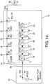
- FIG. 1a shown is a diagram of a wave shaping circuit (WSC) 10 according to a first illustrated embodiment.
- WSC wave shaping circuit
- the WSC 10 is preferably driven by a simple square wave pulse source 12, which can be a separate component (as shown in FIG. 1A ) or which may be combined with the WSC 10 for example on the same IC.
- a simple square wave pulse source 12 can be a separate component (as shown in FIG. 1A ) or which may be combined with the WSC 10 for example on the same IC.
- each of the transmission line sections 14, 16, 18 and 20 preferably has a time delay of 2.5 nanoseconds, and the last open ended transmission line section 22 has a time delay of 1.25 nanoseconds.
- resistors 24, 26, 28, 30 and 32 (which may be collectively known as impedance components for their imparted impedance values) in the tapped lines can have values, such as: 2,625 ⁇ ; 1,500 ⁇ ; 736 ⁇ ; 452 ⁇ and 663 ⁇ , respectively.
- WSC 10 preferably utilizes purely resistive components 24, 26, 28, 30 and 32, but in general they can be impedances comprising reactive components as well (capacitors and/or inductors). Additionally, WSC 10 further includes capacitor 34 determined to have a value of 50 picofarads and a load resistor 35 chosen to have 50 ⁇ resistance.
- the optimal lengths of transmission line sections and resistor values (or generally impedance) for WSC 10 may be analytically calculated by deriving equations for WSC 10. It is noted simulators, such as the MicroCap10, can provide a method to vary circuit parameters in real time while simulating for result optimization.
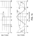
- FIG. 1b simulation results for the WSC 10 of FIG. 1a are shown.
- An input square pulse 36 (depicted as a function of time in nanoseconds) having a time duration t2-t1 is shown.
- a simulated output waveform signal 38 is also shown on the same time scale as the aforementioned input square pulse 36.
- the output waveform signal 38 starts to increase from a zero value at the time t1 (beginning of the pulse 36) to a maximum value at the time t2 (end of the pulse 36). Then it decreases to the zero value at the time t3, where t2-t1 is approximately equal to t3-t2.
- output waveform signal 38 has a desired shape of a raised cosine function.
- Cosine waveform 37 is also depicted in FIG. 1b .
- Cosine waveform 37 is simulated as A1(1+sin(2 ⁇ 20 ⁇ 10 6 (T-37.4))), where T is a time in nanoseconds, and A1 is a scaling constant.
- T is a time in nanoseconds
- A1 is a scaling constant.
- the results indicate approximation between the desired raised cosine pulse waveform 38 with the simulated curve 37 in the overlap region between t1 and t3 (with a maximum at t2). It is to be appreciated that additional transmission line sections may be added if greater waveform fidelity is required.
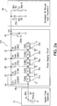
- FIG. 2a shown is a diagram of a wave shaping circuit referenced generally by numeral 200 according to another illustrated embodiment.
- a variation of the raised cosine waveform is simulated.
- This variation preferably corresponds to high bandwidth systems.
- the desired waveform in this example is a pulse having a flat top and edges that follow a raised cosine waveform shape. It is to be understood this is a variation of the example presented in conjunction with FIGS. 1a and 1b .
- WSC 200 driven by a simple square wave pulse source 12 (as was used with WSC 10 in FIG. 1B ).
- the WSC 200 preferably includes capacitor 34a for providing low band filtering to smooth the output waveform signal V 3 .
- each of the transmission lines sections 14a, 16a, 18a and 20a preferably has a time delay of 10 nanoseconds
- the last open ended transmission lines section 22a preferably has a time delay of 5 nanoseconds.
- resistors each preferably has a value of 2,625 ⁇ , 1,500 ⁇ , 736 ⁇ , 452 ⁇ and 663 ⁇ , respectively.
- capacitor 34a preferably has a value of 300 picofarads.
- the output waveform signal V 3 is shown fed to a high bandwidth (HB) circuit 40 having a high input impedance (values of resistive and reactive components are indicated in FIG. 2a using Ohm, Farad and Henry units, respectively).
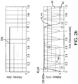
- Results for the WSC 200 of FIG. 2a are shown in FIG. 2b .
- An input square pulse, referenced by numeral 36a (and as shown as a function of time in microseconds) having duration t2 is depicted.
- a stimulated output waveform signal, referenced by numeral 42 is also depicted in FIG. 2B having the same time scale as the input square pulse 36a. It is noted the output waveform signal 42 starts increasing from a zero value at zero time (beginning of the pulse 36a) to a maximum value at the time t1 and stays constant until the time t2 (end of the pulse 36a). Pulse 36a then decreases to the zero value at the time t3. It is seen from FIG. 2b that the signal 42 has a desired shape of the variation of the raised cosine function.
- a cosine waveform 44 is also shown in FIG. 2b .
- the cosine waveform 44 is simulated as A1(1+sin(2 ⁇ 5 ⁇ 10 6 (T-54))), where T is a time in nanoseconds and A1 is a scaling constant.
- T is a time in nanoseconds
- A1 is a scaling constant.
- FIG. 2b the results indicate approximation between the desired variation of the raised cosine pulse waveform 42 with the simulated cosine waveform 44 in the overlap regions between zero and t1, and between t2 and t3. Note, that additional transmission line sections may be added if greater waveform fidelity is required.
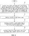
- FIG. 3 shown is a flow chart demonstrating implementation of the various illustrated embodiments. It is noted that the order of steps shown in FIG. 3 is not required, so in principle, the various steps may be performed out of the illustrated order. Also certain steps may be skipped, different steps may be added or substituted, or selected steps or groups of steps may be performed in a separate application following the embodiments described herein.
- a wave shaping circuit (WSC) and an input waveform generator are provided (which may be separate units or combined into one unit, such as an IC).
- the WSC e.g., 10, 200
- the WSC preferably includes transmission line sections consecutively arranged in series and configured to create time delay signals.
- one or more reflected signals of the input waveform signal, and impedance elements are positioned in tapped off ends of the transmission lines sections as described herein.
- the WSC receives an input waveform signal, such as a short pulse signal.
- the WSC generates an output waveform signal of a predefined form by combining, and using the aforesaid tapped off ends of the transmission lines, the time delay and reflected signals.
- a shape of the output waveform signal is preferably smoothed by low band filtering, preferably using a capacitor provided in the WSC.
Landscapes
- Physics & Mathematics (AREA)
- Nonlinear Science (AREA)
- Measurement Of Resistance Or Impedance (AREA)
Claims (15)
- Vorrichtung (10;200), umfassend:Übertragungsleitungsabschnitte (14,16,18,20,22), die in Reihe angeordnet und konfiguriert sind, um Zeitverzögerungssignale eines Eingangswellenformsignals (36) zu erzeugen;Impedanzkomponenten (24,26,28,30,32), die in Leitungen positioniert sind, die an bestimmten Enden der Übertragungsleitungsabschnitte abgegriffen sind, wodurch die Zeitverzögerungssignale jedes Übertragungsleitungsabschnitts über die Impedanzkomponenten kombiniert werden, um ein Ausgangswellenformsignal (38) mit einer vordefinierten Form (37) zu formen; dadurch gekennzeichnet, dass
mindestens einer der Übertragungsleitungsabschnitte (22) eine Länge aufweist, die sich von mindestens einem anderen der Übertragungsleitungsabschnitte (14,16,18,20,22) unterscheidet. - Vorrichtung nach Anspruch 1, wobei jede der Impedanzkomponenten eine Widerstandskomponente einschließt.
- Vorrichtung nach Anspruch 1 oder 2, wobei die Übertragungsleitungsabschnitte ferner konfiguriert sind, um ein oder mehrere reflektierte Signale zu erzeugen, sodass sowohl die Zeitverzögerungssignale als auch die einen oder mehreren reflektierten Signale kombiniert werden, um das Ausgangswellenformsignal mit der vordefinierten Form zu formen.
- Vorrichtung nach einem der vorhergehenden Ansprüche, wobei das Eingangswellenformsignal ein Rechteckimpuls ist und wobei die Vorrichtung ferner einen Rechteckimpulsgenerator (12) umfasst, der konfiguriert ist, um den Rechteckimpuls zu erzeugen.
- Vorrichtung nach einem der vorhergehenden Ansprüche, wobei ein letzter der Übertragungsleitungsabschnitte eine offen endende Übertragungsleitung ist.
- Vorrichtung nach einem der vorhergehenden Ansprüche, ferner umfassend einen Kondensator (35), der konfiguriert ist, um das Ausgangswellenformsignal mit der vordefinierten Form zu filtern, um eine Form des Ausgangswellenformsignals zu glätten.
- Vorrichtung nach einem der vorhergehenden Ansprüche, wobei die Zeitverzögerungssignale jedes Übertragungsleitungsabschnitts resistiv kombiniert werden.
- Vorrichtung nach Anspruch 7, wobei die Zeitverzögerungssignale jedes Übertragungsleitungsabschnitts resistiv kombiniert werden, um das Wellenformsignal mit einer vordefinierten Form unter Verwendung einer trapezförmigen Summierung anzunähern.
- Verfahren, umfassend:Empfangen eines Eingangswellenformsignals (36) in einer Vorrichtung (10;200);Erzeugen von Zeitverzögerungssignalen des Eingangswellenformsignals unter Verwendung von Übertragungsleitungsabschnitten (14,16,18,20,22), die in Reihe angeordnet sind;Erzeugen eines Ausgangswellenformsignals (38) mit einer vordefinierten Form (37) durch das Kombinieren der Zeitverzögerungssignale aus den Übertragungsleitungsabschnitten über Impedanzkomponenten, die in Leitungen positioniert sind, die an bestimmten Enden der Übertragungsleitungsabschnitte abgegriffen sind; unddadurch gekennzeichnet, dass
mindestens eine der Übertragungsleitungen eine Länge aufweist, die sich von den anderen Übertragungsleitungen unterscheidet. - Verfahren nach Anspruch 9, wobei jeder der Übertragungsleitungsabschnitte konfiguriert ist, um ein oder mehrere reflektierte Signale zu erzeugen, wobei sowohl die Zeitverzögerungssignale als auch die einen oder mehreren reflektierten Signale kombiniert werden, um das Ausgangswellenformsignal mit der vordefinierten Form zu formen.
- Verfahren nach Anspruch 9 oder 10, wobei jeder der Übertragungsleitungsabschnitte ein abgegriffenes Ende einschließt, das eine Impedanzkomponente (24,26,28,30,32) aufweist.
- Verfahren nach Anspruch 11, wobei jede der Impedanzkomponenten eine resistive Komponente einschließt.
- Verfahren nach Anspruch 11, wobei das Ausgangswellenformsignal mit der vordefinierten Form auf Grundlage einer Optimierung von einem oder mehreren der Längen der Übertragungsleitungsabschnitte und Werten der Impedanzkomponenten bereitgestellt wird.
- Verfahren nach einem der Ansprüche 11 bis 13, ferner einschließend die Verwendung einer trapezförmigen Summierung über die abgegriffenen Leitungen der Übertragungsleitungsabschnitte, um das Ausgangswellenformsignal mit der vordefinierten Form zu formen.
- Verfahren nach einem der Ansprüche 9 bis 14, wobei die Eingangswellenform ein Rechteckimpulssignal ist.
Applications Claiming Priority (1)
| Application Number | Priority Date | Filing Date | Title |
|---|---|---|---|
| US13/898,223 US8847650B1 (en) | 2013-05-20 | 2013-05-20 | Generating signal waveforms of a predetermined format |
Publications (2)
| Publication Number | Publication Date |
|---|---|
| EP2806559A1 EP2806559A1 (de) | 2014-11-26 |
| EP2806559B1 true EP2806559B1 (de) | 2017-03-08 |
Family
ID=50980114
Family Applications (1)
| Application Number | Title | Priority Date | Filing Date |
|---|---|---|---|
| EP14169136.0A Active EP2806559B1 (de) | 2013-05-20 | 2014-05-20 | Erzeugung von Signalwellenformen mit einer vordefinierten Form |
Country Status (2)
| Country | Link |
|---|---|
| US (1) | US8847650B1 (de) |
| EP (1) | EP2806559B1 (de) |
Family Cites Families (2)
| Publication number | Priority date | Publication date | Assignee | Title |
|---|---|---|---|---|
| JPH1174783A (ja) * | 1997-06-18 | 1999-03-16 | Mitsubishi Electric Corp | 内部クロック信号発生回路、および同期型半導体記憶装置 |
| US7116956B2 (en) * | 2001-02-16 | 2006-10-03 | Cubic Corporation | Power oscillator for control of waveshape and amplitude |
-
2013
- 2013-05-20 US US13/898,223 patent/US8847650B1/en active Active
-
2014
- 2014-05-20 EP EP14169136.0A patent/EP2806559B1/de active Active
Non-Patent Citations (1)
| Title |
|---|
| None * |
Also Published As
| Publication number | Publication date |
|---|---|
| EP2806559A1 (de) | 2014-11-26 |
| US8847650B1 (en) | 2014-09-30 |
Similar Documents
| Publication | Publication Date | Title |
|---|---|---|
| Paul | Solution of the transmission-line equations under the weak-coupling assumption | |
| Surovtsev et al. | Pulse decomposition in the turn of meander line as a new concept of protection against UWB pulses | |
| CN109901066A (zh) | 马达系统辨识方法 | |
| Gazizov et al. | Improved design of modal filter for electronics protection | |
| EP2806559B1 (de) | Erzeugung von Signalwellenformen mit einer vordefinierten Form | |
| CA2496322A1 (en) | Methods for transmitting a waveform having a controllable attenuation and propagation velocity | |
| CN114185014A (zh) | 一种应用于雷达信号处理的并行卷积方法及装置 | |
| CN103744066A (zh) | 数字正交鉴相与匹配滤波的优化方法 | |
| RU2656834C2 (ru) | Усовершенствованная линия задержки, защищающая от сверхкоротких импульсов с увеличенной длительностью | |
| Orduyılmaz et al. | Real-time pulse compression radar waveform generation and digital matched filtering | |
| CN109598060A (zh) | 一种电路板级产品辐射发射电磁兼容仿真方法 | |
| CN205992891U (zh) | 一种可调波瞬态电磁脉冲模拟器装置 | |
| Nosov et al. | Propagation of UWB pulse in two turns of meander microstrip line connected in cascade | |
| CN220543105U (zh) | 一种基于多散射中心的任意目标模拟系统 | |
| CN103543441B (zh) | 基于fpga纳秒级可编程延时电路的数字相关器 | |
| JP2006133210A (ja) | 衝撃応答スペクトルが現れる時間の差が短い衝撃波形の合成方法、及び衝撃応答内訳を求めるデジタルフィルタとそのデジタル逆フィルタ | |
| Beyene et al. | An accurate transient analysis of high-speed package interconnects using convolution technique | |
| Krzikalla et al. | SPICE simulations of uwb pulse stressed protection elements against transient interferences | |
| CN101303610A (zh) | 用于信号发生器取样步长复杂多变的信号离散方法 | |
| CN110445478A (zh) | 一种任意脉宽的脉冲发生装置 | |
| RU2597940C1 (ru) | Линия задержки, защищающая от сверхкоротких импульсов | |
| Ravelo et al. | Cable delay cancellation with low-pass NGD function | |
| CN101499809A (zh) | 接收芯片电路与通信系统 | |
| Zhang et al. | The research of analytical approach for crosstalk of multi-conductor transmission lines | |
| US20070279116A1 (en) | Pulse generator |
Legal Events
| Date | Code | Title | Description |
|---|---|---|---|
| PUAI | Public reference made under article 153(3) epc to a published international application that has entered the european phase |
Free format text: ORIGINAL CODE: 0009012 |
|
| 17P | Request for examination filed |
Effective date: 20140520 |
|
| AK | Designated contracting states |
Kind code of ref document: A1 Designated state(s): AL AT BE BG CH CY CZ DE DK EE ES FI FR GB GR HR HU IE IS IT LI LT LU LV MC MK MT NL NO PL PT RO RS SE SI SK SM TR |
|
| AX | Request for extension of the european patent |
Extension state: BA ME |
|
| R17P | Request for examination filed (corrected) |
Effective date: 20150508 |
|
| RBV | Designated contracting states (corrected) |
Designated state(s): AL AT BE BG CH CY CZ DE DK EE ES FI FR GB GR HR HU IE IS IT LI LT LU LV MC MK MT NL NO PL PT RO RS SE SI SK SM TR |
|
| 17Q | First examination report despatched |
Effective date: 20151210 |
|
| GRAP | Despatch of communication of intention to grant a patent |
Free format text: ORIGINAL CODE: EPIDOSNIGR1 |
|
| INTG | Intention to grant announced |
Effective date: 20160915 |
|
| GRAS | Grant fee paid |
Free format text: ORIGINAL CODE: EPIDOSNIGR3 |
|
| GRAA | (expected) grant |
Free format text: ORIGINAL CODE: 0009210 |
|
| AK | Designated contracting states |
Kind code of ref document: B1 Designated state(s): AL AT BE BG CH CY CZ DE DK EE ES FI FR GB GR HR HU IE IS IT LI LT LU LV MC MK MT NL NO PL PT RO RS SE SI SK SM TR |
|
| REG | Reference to a national code |
Ref country code: GB Ref legal event code: FG4D |
|
| REG | Reference to a national code |
Ref country code: CH Ref legal event code: EP Ref country code: AT Ref legal event code: REF Ref document number: 874368 Country of ref document: AT Kind code of ref document: T Effective date: 20170315 |
|
| REG | Reference to a national code |
Ref country code: IE Ref legal event code: FG4D |
|
| REG | Reference to a national code |
Ref country code: DE Ref legal event code: R096 Ref document number: 602014007299 Country of ref document: DE |
|
| REG | Reference to a national code |
Ref country code: FR Ref legal event code: PLFP Year of fee payment: 4 |
|
| REG | Reference to a national code |
Ref country code: LT Ref legal event code: MG4D |
|
| REG | Reference to a national code |
Ref country code: NL Ref legal event code: MP Effective date: 20170308 |
|
| PG25 | Lapsed in a contracting state [announced via postgrant information from national office to epo] |
Ref country code: GR Free format text: LAPSE BECAUSE OF FAILURE TO SUBMIT A TRANSLATION OF THE DESCRIPTION OR TO PAY THE FEE WITHIN THE PRESCRIBED TIME-LIMIT Effective date: 20170609 Ref country code: FI Free format text: LAPSE BECAUSE OF FAILURE TO SUBMIT A TRANSLATION OF THE DESCRIPTION OR TO PAY THE FEE WITHIN THE PRESCRIBED TIME-LIMIT Effective date: 20170308 Ref country code: HR Free format text: LAPSE BECAUSE OF FAILURE TO SUBMIT A TRANSLATION OF THE DESCRIPTION OR TO PAY THE FEE WITHIN THE PRESCRIBED TIME-LIMIT Effective date: 20170308 Ref country code: LT Free format text: LAPSE BECAUSE OF FAILURE TO SUBMIT A TRANSLATION OF THE DESCRIPTION OR TO PAY THE FEE WITHIN THE PRESCRIBED TIME-LIMIT Effective date: 20170308 Ref country code: NO Free format text: LAPSE BECAUSE OF FAILURE TO SUBMIT A TRANSLATION OF THE DESCRIPTION OR TO PAY THE FEE WITHIN THE PRESCRIBED TIME-LIMIT Effective date: 20170608 |
|
| REG | Reference to a national code |
Ref country code: AT Ref legal event code: MK05 Ref document number: 874368 Country of ref document: AT Kind code of ref document: T Effective date: 20170308 |
|
| PG25 | Lapsed in a contracting state [announced via postgrant information from national office to epo] |
Ref country code: BG Free format text: LAPSE BECAUSE OF FAILURE TO SUBMIT A TRANSLATION OF THE DESCRIPTION OR TO PAY THE FEE WITHIN THE PRESCRIBED TIME-LIMIT Effective date: 20170608 Ref country code: RS Free format text: LAPSE BECAUSE OF FAILURE TO SUBMIT A TRANSLATION OF THE DESCRIPTION OR TO PAY THE FEE WITHIN THE PRESCRIBED TIME-LIMIT Effective date: 20170308 Ref country code: ES Free format text: LAPSE BECAUSE OF FAILURE TO SUBMIT A TRANSLATION OF THE DESCRIPTION OR TO PAY THE FEE WITHIN THE PRESCRIBED TIME-LIMIT Effective date: 20170308 Ref country code: SE Free format text: LAPSE BECAUSE OF FAILURE TO SUBMIT A TRANSLATION OF THE DESCRIPTION OR TO PAY THE FEE WITHIN THE PRESCRIBED TIME-LIMIT Effective date: 20170308 Ref country code: LU Free format text: LAPSE BECAUSE OF NON-PAYMENT OF DUE FEES Effective date: 20170531 Ref country code: LV Free format text: LAPSE BECAUSE OF FAILURE TO SUBMIT A TRANSLATION OF THE DESCRIPTION OR TO PAY THE FEE WITHIN THE PRESCRIBED TIME-LIMIT Effective date: 20170308 |
|
| PG25 | Lapsed in a contracting state [announced via postgrant information from national office to epo] |
Ref country code: NL Free format text: LAPSE BECAUSE OF FAILURE TO SUBMIT A TRANSLATION OF THE DESCRIPTION OR TO PAY THE FEE WITHIN THE PRESCRIBED TIME-LIMIT Effective date: 20170308 |
|
| PG25 | Lapsed in a contracting state [announced via postgrant information from national office to epo] |
Ref country code: EE Free format text: LAPSE BECAUSE OF FAILURE TO SUBMIT A TRANSLATION OF THE DESCRIPTION OR TO PAY THE FEE WITHIN THE PRESCRIBED TIME-LIMIT Effective date: 20170308 Ref country code: SK Free format text: LAPSE BECAUSE OF FAILURE TO SUBMIT A TRANSLATION OF THE DESCRIPTION OR TO PAY THE FEE WITHIN THE PRESCRIBED TIME-LIMIT Effective date: 20170308 Ref country code: IT Free format text: LAPSE BECAUSE OF FAILURE TO SUBMIT A TRANSLATION OF THE DESCRIPTION OR TO PAY THE FEE WITHIN THE PRESCRIBED TIME-LIMIT Effective date: 20170308 Ref country code: AT Free format text: LAPSE BECAUSE OF FAILURE TO SUBMIT A TRANSLATION OF THE DESCRIPTION OR TO PAY THE FEE WITHIN THE PRESCRIBED TIME-LIMIT Effective date: 20170308 Ref country code: RO Free format text: LAPSE BECAUSE OF FAILURE TO SUBMIT A TRANSLATION OF THE DESCRIPTION OR TO PAY THE FEE WITHIN THE PRESCRIBED TIME-LIMIT Effective date: 20170308 Ref country code: CZ Free format text: LAPSE BECAUSE OF FAILURE TO SUBMIT A TRANSLATION OF THE DESCRIPTION OR TO PAY THE FEE WITHIN THE PRESCRIBED TIME-LIMIT Effective date: 20170308 |
|
| PG25 | Lapsed in a contracting state [announced via postgrant information from national office to epo] |
Ref country code: PL Free format text: LAPSE BECAUSE OF FAILURE TO SUBMIT A TRANSLATION OF THE DESCRIPTION OR TO PAY THE FEE WITHIN THE PRESCRIBED TIME-LIMIT Effective date: 20170308 Ref country code: SM Free format text: LAPSE BECAUSE OF FAILURE TO SUBMIT A TRANSLATION OF THE DESCRIPTION OR TO PAY THE FEE WITHIN THE PRESCRIBED TIME-LIMIT Effective date: 20170308 Ref country code: PT Free format text: LAPSE BECAUSE OF FAILURE TO SUBMIT A TRANSLATION OF THE DESCRIPTION OR TO PAY THE FEE WITHIN THE PRESCRIBED TIME-LIMIT Effective date: 20170710 Ref country code: IS Free format text: LAPSE BECAUSE OF FAILURE TO SUBMIT A TRANSLATION OF THE DESCRIPTION OR TO PAY THE FEE WITHIN THE PRESCRIBED TIME-LIMIT Effective date: 20170708 |
|
| REG | Reference to a national code |
Ref country code: DE Ref legal event code: R097 Ref document number: 602014007299 Country of ref document: DE |
|
| REG | Reference to a national code |
Ref country code: CH Ref legal event code: PL |
|
| PLBE | No opposition filed within time limit |
Free format text: ORIGINAL CODE: 0009261 |
|
| STAA | Information on the status of an ep patent application or granted ep patent |
Free format text: STATUS: NO OPPOSITION FILED WITHIN TIME LIMIT |
|
| PG25 | Lapsed in a contracting state [announced via postgrant information from national office to epo] |
Ref country code: DK Free format text: LAPSE BECAUSE OF FAILURE TO SUBMIT A TRANSLATION OF THE DESCRIPTION OR TO PAY THE FEE WITHIN THE PRESCRIBED TIME-LIMIT Effective date: 20170308 Ref country code: MC Free format text: LAPSE BECAUSE OF FAILURE TO SUBMIT A TRANSLATION OF THE DESCRIPTION OR TO PAY THE FEE WITHIN THE PRESCRIBED TIME-LIMIT Effective date: 20170308 |
|
| 26N | No opposition filed |
Effective date: 20171211 |
|
| REG | Reference to a national code |
Ref country code: IE Ref legal event code: MM4A |
|
| PG25 | Lapsed in a contracting state [announced via postgrant information from national office to epo] |
Ref country code: CH Free format text: LAPSE BECAUSE OF NON-PAYMENT OF DUE FEES Effective date: 20170531 Ref country code: LI Free format text: LAPSE BECAUSE OF NON-PAYMENT OF DUE FEES Effective date: 20170531 Ref country code: SI Free format text: LAPSE BECAUSE OF FAILURE TO SUBMIT A TRANSLATION OF THE DESCRIPTION OR TO PAY THE FEE WITHIN THE PRESCRIBED TIME-LIMIT Effective date: 20170308 |
|
| PG25 | Lapsed in a contracting state [announced via postgrant information from national office to epo] |
Ref country code: LU Free format text: LAPSE BECAUSE OF NON-PAYMENT OF DUE FEES Effective date: 20170520 |
|
| REG | Reference to a national code |
Ref country code: FR Ref legal event code: PLFP Year of fee payment: 5 |
|
| REG | Reference to a national code |
Ref country code: BE Ref legal event code: MM Effective date: 20170531 |
|
| PG25 | Lapsed in a contracting state [announced via postgrant information from national office to epo] |
Ref country code: IE Free format text: LAPSE BECAUSE OF NON-PAYMENT OF DUE FEES Effective date: 20170520 |
|
| PG25 | Lapsed in a contracting state [announced via postgrant information from national office to epo] |
Ref country code: BE Free format text: LAPSE BECAUSE OF NON-PAYMENT OF DUE FEES Effective date: 20170531 |
|
| PG25 | Lapsed in a contracting state [announced via postgrant information from national office to epo] |
Ref country code: MT Free format text: LAPSE BECAUSE OF NON-PAYMENT OF DUE FEES Effective date: 20170520 |
|
| PG25 | Lapsed in a contracting state [announced via postgrant information from national office to epo] |
Ref country code: HU Free format text: LAPSE BECAUSE OF FAILURE TO SUBMIT A TRANSLATION OF THE DESCRIPTION OR TO PAY THE FEE WITHIN THE PRESCRIBED TIME-LIMIT; INVALID AB INITIO Effective date: 20140520 |
|
| PG25 | Lapsed in a contracting state [announced via postgrant information from national office to epo] |
Ref country code: CY Free format text: LAPSE BECAUSE OF FAILURE TO SUBMIT A TRANSLATION OF THE DESCRIPTION OR TO PAY THE FEE WITHIN THE PRESCRIBED TIME-LIMIT Effective date: 20170308 |
|
| PG25 | Lapsed in a contracting state [announced via postgrant information from national office to epo] |
Ref country code: MK Free format text: LAPSE BECAUSE OF FAILURE TO SUBMIT A TRANSLATION OF THE DESCRIPTION OR TO PAY THE FEE WITHIN THE PRESCRIBED TIME-LIMIT Effective date: 20170308 |
|
| PG25 | Lapsed in a contracting state [announced via postgrant information from national office to epo] |
Ref country code: TR Free format text: LAPSE BECAUSE OF FAILURE TO SUBMIT A TRANSLATION OF THE DESCRIPTION OR TO PAY THE FEE WITHIN THE PRESCRIBED TIME-LIMIT Effective date: 20170308 |
|
| PG25 | Lapsed in a contracting state [announced via postgrant information from national office to epo] |
Ref country code: AL Free format text: LAPSE BECAUSE OF FAILURE TO SUBMIT A TRANSLATION OF THE DESCRIPTION OR TO PAY THE FEE WITHIN THE PRESCRIBED TIME-LIMIT Effective date: 20170308 |
|
| REG | Reference to a national code |
Ref country code: DE Ref legal event code: R082 Ref document number: 602014007299 Country of ref document: DE |
|
| P01 | Opt-out of the competence of the unified patent court (upc) registered |
Effective date: 20230522 |
|
| PGFP | Annual fee paid to national office [announced via postgrant information from national office to epo] |
Ref country code: DE Payment date: 20250423 Year of fee payment: 12 |
|
| PGFP | Annual fee paid to national office [announced via postgrant information from national office to epo] |
Ref country code: GB Payment date: 20250423 Year of fee payment: 12 |
|
| PGFP | Annual fee paid to national office [announced via postgrant information from national office to epo] |
Ref country code: FR Payment date: 20250423 Year of fee payment: 12 |