EP2806466A2 - Herstellungsverfahren für transparente leitfähige Schicht, Vorrichtung dafür und transparente leitfähige Schicht daraus - Google Patents
Herstellungsverfahren für transparente leitfähige Schicht, Vorrichtung dafür und transparente leitfähige Schicht daraus Download PDFInfo
- Publication number
- EP2806466A2 EP2806466A2 EP14168884.6A EP14168884A EP2806466A2 EP 2806466 A2 EP2806466 A2 EP 2806466A2 EP 14168884 A EP14168884 A EP 14168884A EP 2806466 A2 EP2806466 A2 EP 2806466A2
- Authority
- EP
- European Patent Office
- Prior art keywords
- transparent
- film
- pattern groove
- conductive
- transparent film
- Prior art date
- Legal status (The legal status is an assumption and is not a legal conclusion. Google has not performed a legal analysis and makes no representation as to the accuracy of the status listed.)
- Granted
Links
Images




Classifications
-
- H—ELECTRICITY
- H01—ELECTRIC ELEMENTS
- H01B—CABLES; CONDUCTORS; INSULATORS; SELECTION OF MATERIALS FOR THEIR CONDUCTIVE, INSULATING OR DIELECTRIC PROPERTIES
- H01B5/00—Non-insulated conductors or conductive bodies characterised by their form
- H01B5/14—Non-insulated conductors or conductive bodies characterised by their form comprising conductive layers or films on insulating-supports
-
- H—ELECTRICITY
- H05—ELECTRIC TECHNIQUES NOT OTHERWISE PROVIDED FOR
- H05K—PRINTED CIRCUITS; CASINGS OR CONSTRUCTIONAL DETAILS OF ELECTRIC APPARATUS; MANUFACTURE OF ASSEMBLAGES OF ELECTRICAL COMPONENTS
- H05K3/00—Apparatus or processes for manufacturing printed circuits
- H05K3/10—Apparatus or processes for manufacturing printed circuits in which conductive material is applied to the insulating support in such a manner as to form the desired conductive pattern
- H05K3/12—Apparatus or processes for manufacturing printed circuits in which conductive material is applied to the insulating support in such a manner as to form the desired conductive pattern using thick film techniques, e.g. printing techniques to apply the conductive material or similar techniques for applying conductive paste or ink patterns
- H05K3/1258—Apparatus or processes for manufacturing printed circuits in which conductive material is applied to the insulating support in such a manner as to form the desired conductive pattern using thick film techniques, e.g. printing techniques to apply the conductive material or similar techniques for applying conductive paste or ink patterns by using a substrate provided with a shape pattern, e.g. grooves, banks, resist pattern
-
- H—ELECTRICITY
- H01—ELECTRIC ELEMENTS
- H01B—CABLES; CONDUCTORS; INSULATORS; SELECTION OF MATERIALS FOR THEIR CONDUCTIVE, INSULATING OR DIELECTRIC PROPERTIES
- H01B13/00—Apparatus or processes specially adapted for manufacturing conductors or cables
-
- H—ELECTRICITY
- H05—ELECTRIC TECHNIQUES NOT OTHERWISE PROVIDED FOR
- H05K—PRINTED CIRCUITS; CASINGS OR CONSTRUCTIONAL DETAILS OF ELECTRIC APPARATUS; MANUFACTURE OF ASSEMBLAGES OF ELECTRICAL COMPONENTS
- H05K2203/00—Indexing scheme relating to apparatus or processes for manufacturing printed circuits covered by H05K3/00
- H05K2203/01—Tools for processing; Objects used during processing
- H05K2203/0104—Tools for processing; Objects used during processing for patterning or coating
- H05K2203/0108—Male die used for patterning, punching or transferring
-
- H—ELECTRICITY
- H05—ELECTRIC TECHNIQUES NOT OTHERWISE PROVIDED FOR
- H05K—PRINTED CIRCUITS; CASINGS OR CONSTRUCTIONAL DETAILS OF ELECTRIC APPARATUS; MANUFACTURE OF ASSEMBLAGES OF ELECTRICAL COMPONENTS
- H05K2203/00—Indexing scheme relating to apparatus or processes for manufacturing printed circuits covered by H05K3/00
- H05K2203/09—Treatments involving charged particles
- H05K2203/095—Plasma, e.g. for treating a substrate to improve adhesion with a conductor or for cleaning holes
-
- H—ELECTRICITY
- H05—ELECTRIC TECHNIQUES NOT OTHERWISE PROVIDED FOR
- H05K—PRINTED CIRCUITS; CASINGS OR CONSTRUCTIONAL DETAILS OF ELECTRIC APPARATUS; MANUFACTURE OF ASSEMBLAGES OF ELECTRICAL COMPONENTS
- H05K2203/00—Indexing scheme relating to apparatus or processes for manufacturing printed circuits covered by H05K3/00
- H05K2203/15—Position of the PCB during processing
- H05K2203/1545—Continuous processing, i.e. involving rolls moving a band-like or solid carrier along a continuous production path
-
- H—ELECTRICITY
- H05—ELECTRIC TECHNIQUES NOT OTHERWISE PROVIDED FOR
- H05K—PRINTED CIRCUITS; CASINGS OR CONSTRUCTIONAL DETAILS OF ELECTRIC APPARATUS; MANUFACTURE OF ASSEMBLAGES OF ELECTRICAL COMPONENTS
- H05K3/00—Apparatus or processes for manufacturing printed circuits
- H05K3/0011—Working of insulating substrates or insulating layers
- H05K3/0017—Etching of the substrate by chemical or physical means
- H05K3/0026—Etching of the substrate by chemical or physical means by laser ablation
- H05K3/0032—Etching of the substrate by chemical or physical means by laser ablation of organic insulating material
Definitions
- the present invention relates to a transparent conductive film manufacturing method which forms a minute conductive pattern on a transparent substrate, an apparatus thereof, and a transparent conductive film thereof.
- a minute pattern is formed on a transparent substrate and the minute pattern is filled with a metal paste to form a transparent conductive film.
- a concave pattern groove of the minute pattern is formed in a synthetic resin film and the pattern groove is filled with the metal paste to form a transparent electrode.
- the metal paste which is filled and smeared outside the pattern groove is removed by using a blade.
- a blade process using a blade is included so that a process of manufacturing a transparent electrode becomes complicated.
- the present invention has been made in an effort to provide a transparent conductive film manufacturing method which easily fills a metal paste in a pattern groove and simplifies the process.
- the present invention has also been made in an effort to provide an apparatus which implements the transparent conductive film manufacturing method.
- the present invention has also been made in an effort to provide a transparent conductive film manufactured by the transparent conductive film manufacturing method and the apparatus thereof.
- An exemplary embodiment of the present invention provides a transparent conductive film manufacturing method including: a first step of processing one surface of a transparent film with plasma to form a hydrophobic surface with minute protrusions and grooves; a second step of patterning a hydrophilic pattern groove on one surface of the transparent film; a third step of dispensing a conductive paste onto the pattern groove of the transparent film; and a fourth step of drying and hardening the conductive paste.
- the second step may pattern the pattern groove using a laser head by a scribing method.
- the third step may dispense the conductive paste to the pattern groove using a dispenser by a drop method.
- the second step may pattern the pattern groove using a roll imprinter by an imprinting method.
- a transparent conductive film manufacturing apparatus including: an unwinder which supplies a transparent film; a plasma processing unit which processes one surface of the transparent film which is supplied by the unwinder with plasma to form a hydrophobic surface with minute protrusions and grooves; a patterning unit which patterns a hydrophilic pattern groove on one surface of the transparent film which passes through the plasma processing unit; a dispensing unit which dispenses the conductive paste to the pattern groove of the transparent film which passes through the patterning unit; a drying unit which dries and hardens the conductive paste on the transparent film which passes through the dispensing unit; and a winder which winds the transparent conductive film which is manufactured by passing through the drying unit.
- the patterning unit may be formed as a laser head or a roll imprinter.
- a transparent conductive film including: a transparent film which includes a hydrophobic part which is formed with minute protrusions and grooves on one surface thereof by plasma processing and a hydrophilic part which is formed between the hydrophobic parts as a pattern groove; and a conductive part which is formed by a conductive paste which fills the pattern groove, wherein a lowest limit value of the line width of the conductive part is 0.6 ⁇ m.
- the lowest limit value of the line width of the conductive part may be 5 ⁇ m.
- the transparent film may be one of PI, PET, PEN, and PI
- the conductive paste may be one of Ag, Al, and a conductive polymer.
- a difference in a height between an upper edge of the protrusion and a bottom of the groove may be 1 to 10 nm.
- plasma processing is performed on one surface of the transparent film to impart hydrophobicity thereto, and the pattern groove is patterned to partially impart hydrophilicity thereto to dispense the conductive paste to the hydrophilic pattern groove while preventing the conductive paste from remaining in a hydrophobic part to dry and harden the conductive paste.
- the transparent conductive film is manufactured.
- the hydrophilic pattern groove which is enclosed by the hydrophobic part is easily filled with the metal paste and the metal paste is completely prevented from being applied in the hydrophobic part so that a blade process which removes the remaining metal paste is omitted, thereby simplifying the manufacturing process.
- FIG. 1 is a flowchart of a transparent conductive film manufacturing method according to a first exemplary embodiment of the present invention.
- a transparent conductive film manufacturing method includes a first step ST1 of processing a transparent film 1 with plasma, a second step ST2 of patterning a pattern groove 2, a third step ST3 of dispensing a conductive paste 3, and a fourth step ST4 of drying and hardening the dispensed conductive paste.
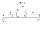
- FIG. 2 is a schematic diagram illustrating a transparent conductive film manufacturing apparatus which implements the manufacturing method of FIG. 1 .
- the transparent conductive film manufacturing apparatus 100 includes an unwinder 10, a plasma processing unit 20, a patterning unit 30, a dispensing unit 40, a drying unit 50, and a winder 60.
- plasma processing is performed on one surface of the transparent film 1 using the plasma processing unit 20 to form minute protrusions and grooves on the one surface of the transparent film 1.
- the minute protrusions and grooves impart hydrophobicity to the one surface of the transparent film 1.
- the plasma processing unit 20 may be configured as various types so as to perform plasma processing on the one surface of the transparent film 1 which is supplied to the unwinder 10.
- the first step ST1 includes a process of supplying the transparent film 1 in the unwinder 10.
- the unwinder 10 supplies the transparent film 1 to the plasma processing unit 20.
- the transparent film 1 may be formed of polyimide (PI), polyethylene terephthalate (PET), polyethylene naphthalate (PEN), or polycarbonate (PC), and may have various thicknesses depending on purposes. Further, when the transparent film 1 is processed with plasma at a predetermined intensity for 30 seconds to one minute, the transparent film 1 may have appropriate hydrophobicity. As the plasma processing is performed on a surface of the transparent film 1 for 30 seconds to one minute, a contact angle of 100 degrees or higher is formed with respect to a water droplet, so that the transparent film may have the hydrophobicity.
- PI polyimide
- PET polyethylene terephthalate
- PEN polyethylene naphthalate
- PC polycarbonate
- the protrusions and the grooves are insufficiently formed so that the transparent film 1 may not have required hydrophobicity. Further, when the plasma processing is performed on the transparent film 1 at the same intensity for three minutes or longer, the protrusions and the grooves which are formed on the surface of the transparent film 1 are removed so that the transparent film 1 may not have required hydrophobicity.
- the plasma processing unit 20 forms the minute protrusions and grooves on the surface of the transparent film 10 using a fluorine-based gas, for example, CF 4 , HF, NF 3 , or OF 2 to impart the hydrophobicity.
- a fluorine-based gas for example, CF 4 , HF, NF 3 , or OF 2 to impart the hydrophobicity.
- a difference in a height between an upper edge of the minute protrusion and a bottom of the groove, which are formed on the surface of the transparent film 10, is 1 to 10 nm.
- the difference in depth When the difference in depth is 1 nm or less, it is hard to process the surface of the transparent film 10, and when the difference in depth is 10 nm or more, the surface of the transparent film 10 may have hydrophilicity.
- the difference in depth of the upper edge of the minute protrusion and the bottom of the groove may impart the hydrophobicity to the surface of the transparent film 10 in different ranges depending on the gas that is used for the plasma processing.
- the second step ST2 patterns the pattern groove 2 on one surface of the transparent film 1 using the patterning unit 30.
- the pattern groove 2 has relative hydrophilicity as compared with other hydrophobic portions of the transparent film 1.
- the patterning unit 30 may be formed by a laser head, and the second step ST2 may pattern the pattern groove 2 using the laser head by a scribing method.
- the patterning unit 30 may be formed as various types so as to pattern the pattern groove 2 on one surface of the transparent film 1 which passes through the plasma processing unit 20.
- the pattern groove 2 is formed on the surface of the transparent film 1 having hydrophobicity so that the one surface of the transparent film 1 is divided into a hydrophobic part and a hydrophilic part having hydrophilicity. That is, the hydrophobic part is formed on the one surface of the transparent film 1 by the plasma processing as the minute protrusions and grooves, and the hydrophilic part is formed between the hydrophobic parts as the pattern groove 2.
- the pattern groove 2 may be formed to have a rectangular shape on a cross-section of the transparent film 1.
- the pattern groove 2 on the rectangle cross-section increases an amount of conductive paste 3 to fill to improve the conductivity in the transparent conductive film P1.
- the dispensing unit 40 dispenses the conductive paste 3 to the pattern groove 2 of the transparent film 1.
- the conductive paste 3 imparts the conductivity to a transparent conductive film P1.
- the dispensing unit 40 may be formed as a paste dispenser, and in the third step ST3, the dispenser dispenses the conductive paste 3 to the pattern groove 2 by a drop method.
- the dispensing unit 40 is formed to dispense the conductive paste 3 to the pattern groove 2 of the transparent film 1 which passes through the patterning unit 30.
- the conductive paste 3 may be formed of Ag, Al, or a conductive polymer.
- the conductive paste 3 may fill the pattern groove 2 to form a rectangular conductive part on the cross-section of the transparent conductive film P1.
- the transparent film 1 may form a transparent part in the transparent conductive film P1. Accordingly, the transparent conductive film may be used as a transparent electrode of a display device.
- the conductive part formed by the conductive paste 3 has a line width corresponding to a line width W of the pattern groove 3 so that the conductive part has excellent conductivity.
- the conductive paste 3 which is dispensed by a drop method fills only the pattern groove 2 which forms the hydrophilic part to be convex and then is dried and hardened to increase the density of the conductive part, but is not provided at the outside of the pattern groove which forms the hydrophilic part.
- the third step ST3 omits the blading process of the related art.
- the drying unit 50 dries and hardens the conductive paste 3.
- the transparent film 1 which forms the transparent part of the transparent conductive film P1 has heat resistance so as to not be deformed during the drying process.
- the drying unit 50 may be formed as an infrared dryer, and in the fourth step ST4, the dryer hardens and dries the conductive paste 3 which is dispensed to the pattern groove 2 by an infrared drying method.
- the drying unit 50 is formed to dry and harden the conductive paste 3 on the transparent film 1 which passes through the dispensing unit 40.
- the dried conductive paste 3 is hardened only in the pattern groove 2 which forms the hydrophilic part to be flat or concave. Accordingly, the transparent conductive film P1 is completely formed.
- the fourth step ST4 includes a process of winding the dried and hardened transparent film 1. That is, the winder 60 winds the manufactured transparent conductive film P1.
- a lowest limit value of the line width W of the conductive part formed by the pattern groove 2 and the conductive paste 3 which fills the pattern groove 3 is 0.6 ⁇ m.
- the transparent conductive film P1 has excellent translucency when the line width W of the pattern groove 3 and the conductive part is smaller.
- the pattern groove 2 needs to be formed as fine as possible so that a lowest limit value of the pattern groove 2 is meaningful.
- the lowest limit value of the pattern groove 2 is 0.6 to 30 ⁇ m.
- the line width W of the pattern groove 2 is too large, the translucency is lowered so that the transparent conductive film P1 may not fulfill its purpose.
- FIG. 3 is a flowchart of a transparent conductive film manufacturing method according to a second exemplary embodiment of the present invention
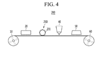
- FIG. 4 is a schematic diagram illustrating a transparent conductive film manufacturing apparatus 200 which implements the manufacturing method of FIG. 3 .
- a patterning unit 230 includes a roll imprinter.
- a pattern groove 22 is patterned on one surface of a transparent film 1 which is hydrophobically processed by an imprinting method of the roll imprinter as the plasma-processed transparent film 1 is supplied.
- the pattern groove 22 may be formed to have a triangular shape on a cross-section of the transparent film 1.
- the pattern groove 11 having a triangular cross-section may reduce an amount of consumed conductive paste 23 as compared with the rectangular cross-section having the same line width W, and allows the imprinting roll to be easily manufactured in the roll imprinter 231.
- a lowest limit value of the line width W of the pattern groove 22 may be 5 ⁇ m. That is, the roll imprinter forms the pattern groove 22 to have a larger line width than a line width of a pattern groove formed by a laser head. For example, the lowest limit value of the pattern groove 22 is 5 to 30 ⁇ m.
- the first and second exemplary embodiments exemplify the pattern grooves 2 and 22 which are formed to have a rectangular shape or a triangular shape on the cross-section of the transparent film 1. Even though not illustrated, the pattern groove may be formed to be a partial cross-section of a circle, a pentagon, or a hexagon.
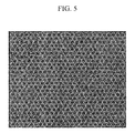
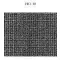
- FIGS. 5 to 10 are top plan views of transparent conductive films manufactured according to the first and second exemplary embodiments.
- a white portion indicates a conductive part of a pattern.
- a transparent conductive film P3 includes a conductive part having a circular pattern.
- a transparent conductive film P4 includes a conductive part having a triangular pattern.
- a transparent conductive film P5 includes a conductive part having a honeycomb pattern.
- a transparent conductive film P6 includes a conductive part having a comb pattern.
- a transparent conductive film P6 includes a conductive part having a cross pattern.
- a transparent conductive film P7 includes a conductive part having a mesh pattern.
- the transparent conductive films P3 to P7 may be formed such that the line width of the conductive part is 0.6, 1, 5, 10, or 30 ⁇ m depending on the conductivity of the conductive paste, and the pattern interval is 100, 200, 300, 400, or 500 ⁇ m, or 2 mm, depending on the translucency.
Landscapes
- Engineering & Computer Science (AREA)
- Manufacturing & Machinery (AREA)
- Microelectronics & Electronic Packaging (AREA)
- Manufacturing Of Electric Cables (AREA)
Applications Claiming Priority (1)
| Application Number | Priority Date | Filing Date | Title |
|---|---|---|---|
| KR1020130057253A KR101357284B1 (ko) | 2013-05-21 | 2013-05-21 | 투명전도필름 제조 방법, 그 장치 및 그 투명전도필름 |
Publications (3)
| Publication Number | Publication Date |
|---|---|
| EP2806466A2 true EP2806466A2 (de) | 2014-11-26 |
| EP2806466A3 EP2806466A3 (de) | 2015-04-29 |
| EP2806466B1 EP2806466B1 (de) | 2016-09-14 |
Family
ID=50146676
Family Applications (1)
| Application Number | Title | Priority Date | Filing Date |
|---|---|---|---|
| EP14168884.6A Active EP2806466B1 (de) | 2013-05-21 | 2014-05-19 | Herstellungsverfahren für transparente leitfähige Schicht, Vorrichtung dafür und transparente leitfähige Schicht daraus |
Country Status (2)
| Country | Link |
|---|---|
| EP (1) | EP2806466B1 (de) |
| KR (1) | KR101357284B1 (de) |
Cited By (2)
| Publication number | Priority date | Publication date | Assignee | Title |
|---|---|---|---|---|
| EP3624571A1 (de) * | 2018-09-14 | 2020-03-18 | Nederlandse Organisatie voor toegepast- natuurwetenschappelijk onderzoek TNO | Verfahren zur herstellung gedruckter leiterbahnen auf einem objekt und 3d-gedruckte elektronik |
| CN111354508A (zh) * | 2016-07-15 | 2020-06-30 | 昇印光电(昆山)股份有限公司 | 一种柔性电极薄膜及应用 |
Families Citing this family (2)
| Publication number | Priority date | Publication date | Assignee | Title |
|---|---|---|---|---|
| KR102320219B1 (ko) * | 2016-09-13 | 2021-11-03 | 한국전자통신연구원 | 3차원 프린팅 방법 |
| US12319385B2 (en) | 2021-05-12 | 2025-06-03 | Montana State University | Process for establishing uniform liquid films on polar and non-polar substrates |
Family Cites Families (7)
| Publication number | Priority date | Publication date | Assignee | Title |
|---|---|---|---|---|
| JP2008028164A (ja) * | 2006-07-21 | 2008-02-07 | Asahi Glass Co Ltd | 透明導電膜およびその製造方法、ならびに透明導電膜を用いた電磁遮蔽体およびディスプレイ装置 |
| CN103465525B (zh) * | 2006-12-27 | 2015-10-21 | 日立化成株式会社 | 凹版和使用该凹版的带有导体层图形的基材 |
| KR20090034193A (ko) * | 2007-10-02 | 2009-04-07 | 주식회사 쏠리스 | 진공 롤투롤 증착장치 및 그 증착방법 |
| KR100999506B1 (ko) * | 2008-09-09 | 2010-12-09 | 삼성전기주식회사 | 인쇄회로기판 및 그 제조 방법 |
| KR101148144B1 (ko) * | 2009-09-07 | 2012-05-23 | 고려대학교 산학협력단 | 플렉시블 가스 배리어 필름, 그 제조방법 및 이를 이용한 플렉시블 디스플레이 소자 |
| JP5562747B2 (ja) * | 2010-07-13 | 2014-07-30 | 富士フイルム株式会社 | 導電膜の製造方法 |
| KR101164061B1 (ko) * | 2010-10-22 | 2012-07-12 | 한국과학기술원 | 패턴 제조 방법 및 패턴 전사 장치, 이를 적용한 플렉서블 디스플레이 패널, 플렉서블 태양전지, 전자책, 박막 트랜지스터, 전자파 차폐시트, 플렉서블 인쇄회로기판 |
-
2013
- 2013-05-21 KR KR1020130057253A patent/KR101357284B1/ko active Active
-
2014
- 2014-05-19 EP EP14168884.6A patent/EP2806466B1/de active Active
Non-Patent Citations (1)
| Title |
|---|
| None |
Cited By (4)
| Publication number | Priority date | Publication date | Assignee | Title |
|---|---|---|---|---|
| CN111354508A (zh) * | 2016-07-15 | 2020-06-30 | 昇印光电(昆山)股份有限公司 | 一种柔性电极薄膜及应用 |
| CN111354508B (zh) * | 2016-07-15 | 2022-08-19 | 昇印光电(昆山)股份有限公司 | 一种柔性电极薄膜及应用 |
| EP3624571A1 (de) * | 2018-09-14 | 2020-03-18 | Nederlandse Organisatie voor toegepast- natuurwetenschappelijk onderzoek TNO | Verfahren zur herstellung gedruckter leiterbahnen auf einem objekt und 3d-gedruckte elektronik |
| WO2020055253A1 (en) * | 2018-09-14 | 2020-03-19 | Nederlandse Organisatie Voor Toegepast- Natuurwetenschappelijk Onderzoek Tno | A process for the manufacturing of printed conductive tracks on an object and 3d printed electronics |
Also Published As
| Publication number | Publication date |
|---|---|
| KR101357284B1 (ko) | 2014-01-29 |
| EP2806466B1 (de) | 2016-09-14 |
| EP2806466A3 (de) | 2015-04-29 |
Similar Documents
| Publication | Publication Date | Title |
|---|---|---|
| JP6895129B2 (ja) | 蒸着マスクの製造方法および蒸着マスク | |
| EP2806466B1 (de) | Herstellungsverfahren für transparente leitfähige Schicht, Vorrichtung dafür und transparente leitfähige Schicht daraus | |
| US10562273B2 (en) | Cover glass lamination structure and manufacturing method thereof | |
| KR20150099832A (ko) | 성막 마스크의 제조 방법 | |
| CN102237333A (zh) | 导电元件及其制造方法、配线元件、信息输入装置 | |
| US10031414B2 (en) | Template, method of manufacturing the same, and imprint method | |
| JP2013161816A (ja) | パターン形成方法 | |
| JP6676051B2 (ja) | 造形装置および造形方法 | |
| JP6222113B2 (ja) | 薄膜形成方法及び薄膜形成装置 | |
| KR101963886B1 (ko) | 잉크젯 인쇄를 이용한 미세 전극 제작 방법 | |
| JP2016110942A (ja) | ナノ撥液構造を有する隔壁、その隔壁を用いた有機el素子、およびそれらの製造方法 | |
| JP2019101412A (ja) | レンズの膜形成方法とフレネルレンズ | |
| KR20150106322A (ko) | 막 형성방법 및 막 형성장치 | |
| JP2005260216A5 (de) | ||
| US20120141734A1 (en) | Matte-surface substrate and manufacturing method thereof | |
| KR101279472B1 (ko) | 깊이가 향상된 패턴을 갖는 유리 장식재의 제조 방법 | |
| JP6279430B2 (ja) | テンプレート、テンプレート形成方法および半導体装置の製造方法 | |
| WO2019025453A1 (de) | Verfahren zum herstellen eines optoelektronischen bauelements | |
| KR20140015056A (ko) | 패드 인쇄법을 위한 미세 요철 패턴 구조을 구비하는 원판 및 이의 제조 방법 | |
| JP2001062362A (ja) | ペースト塗布方法及びペースト塗布装置 | |
| KR101431225B1 (ko) | 잉크 전사를 통한 패턴 형성방법 | |
| KR101265147B1 (ko) | 개선된 인쇄롤 상의 인쇄 패턴 형성 장치 및 방법 | |
| JP6757241B2 (ja) | パターン形成方法及びレプリカモールドの製造方法 | |
| JP6322375B2 (ja) | 記録物および記録物製造装置 | |
| TW201503355A (zh) | 製造有機電致發光裝置之方法 |
Legal Events
| Date | Code | Title | Description |
|---|---|---|---|
| PUAI | Public reference made under article 153(3) epc to a published international application that has entered the european phase |
Free format text: ORIGINAL CODE: 0009012 |
|
| 17P | Request for examination filed |
Effective date: 20140519 |
|
| AK | Designated contracting states |
Kind code of ref document: A2 Designated state(s): AL AT BE BG CH CY CZ DE DK EE ES FI FR GB GR HR HU IE IS IT LI LT LU LV MC MK MT NL NO PL PT RO RS SE SI SK SM TR |
|
| AX | Request for extension of the european patent |
Extension state: BA ME |
|
| PUAL | Search report despatched |
Free format text: ORIGINAL CODE: 0009013 |
|
| AK | Designated contracting states |
Kind code of ref document: A3 Designated state(s): AL AT BE BG CH CY CZ DE DK EE ES FI FR GB GR HR HU IE IS IT LI LT LU LV MC MK MT NL NO PL PT RO RS SE SI SK SM TR |
|
| AX | Request for extension of the european patent |
Extension state: BA ME |
|
| RIC1 | Information provided on ipc code assigned before grant |
Ipc: H01L 31/18 20060101ALI20150320BHEP Ipc: H01L 31/0224 20060101AFI20150320BHEP |
|
| RBV | Designated contracting states (corrected) |
Designated state(s): AL AT BE BG CH CY CZ DE DK EE ES FI FR GB GR HR HU IE IS IT LI LT LU LV MC MK MT NL NO PL PT RO RS SE SI SK SM TR |
|
| GRAP | Despatch of communication of intention to grant a patent |
Free format text: ORIGINAL CODE: EPIDOSNIGR1 |
|
| INTG | Intention to grant announced |
Effective date: 20160405 |
|
| GRAS | Grant fee paid |
Free format text: ORIGINAL CODE: EPIDOSNIGR3 |
|
| GRAA | (expected) grant |
Free format text: ORIGINAL CODE: 0009210 |
|
| AK | Designated contracting states |
Kind code of ref document: B1 Designated state(s): AL AT BE BG CH CY CZ DE DK EE ES FI FR GB GR HR HU IE IS IT LI LT LU LV MC MK MT NL NO PL PT RO RS SE SI SK SM TR |
|
| REG | Reference to a national code |
Ref country code: GB Ref legal event code: FG4D |
|
| REG | Reference to a national code |
Ref country code: CH Ref legal event code: EP |
|
| REG | Reference to a national code |
Ref country code: IE Ref legal event code: FG4D |
|
| REG | Reference to a national code |
Ref country code: AT Ref legal event code: REF Ref document number: 829828 Country of ref document: AT Kind code of ref document: T Effective date: 20161015 |
|
| REG | Reference to a national code |
Ref country code: DE Ref legal event code: R096 Ref document number: 602014003581 Country of ref document: DE |
|
| REG | Reference to a national code |
Ref country code: LT Ref legal event code: MG4D |
|
| REG | Reference to a national code |
Ref country code: NL Ref legal event code: MP Effective date: 20160914 |
|
| PG25 | Lapsed in a contracting state [announced via postgrant information from national office to epo] |
Ref country code: NO Free format text: LAPSE BECAUSE OF FAILURE TO SUBMIT A TRANSLATION OF THE DESCRIPTION OR TO PAY THE FEE WITHIN THE PRESCRIBED TIME-LIMIT Effective date: 20161214 Ref country code: RS Free format text: LAPSE BECAUSE OF FAILURE TO SUBMIT A TRANSLATION OF THE DESCRIPTION OR TO PAY THE FEE WITHIN THE PRESCRIBED TIME-LIMIT Effective date: 20160914 Ref country code: FI Free format text: LAPSE BECAUSE OF FAILURE TO SUBMIT A TRANSLATION OF THE DESCRIPTION OR TO PAY THE FEE WITHIN THE PRESCRIBED TIME-LIMIT Effective date: 20160914 Ref country code: HR Free format text: LAPSE BECAUSE OF FAILURE TO SUBMIT A TRANSLATION OF THE DESCRIPTION OR TO PAY THE FEE WITHIN THE PRESCRIBED TIME-LIMIT Effective date: 20160914 Ref country code: LT Free format text: LAPSE BECAUSE OF FAILURE TO SUBMIT A TRANSLATION OF THE DESCRIPTION OR TO PAY THE FEE WITHIN THE PRESCRIBED TIME-LIMIT Effective date: 20160914 |
|
| REG | Reference to a national code |
Ref country code: AT Ref legal event code: MK05 Ref document number: 829828 Country of ref document: AT Kind code of ref document: T Effective date: 20160914 |
|
| PG25 | Lapsed in a contracting state [announced via postgrant information from national office to epo] |
Ref country code: LV Free format text: LAPSE BECAUSE OF FAILURE TO SUBMIT A TRANSLATION OF THE DESCRIPTION OR TO PAY THE FEE WITHIN THE PRESCRIBED TIME-LIMIT Effective date: 20160914 Ref country code: SE Free format text: LAPSE BECAUSE OF FAILURE TO SUBMIT A TRANSLATION OF THE DESCRIPTION OR TO PAY THE FEE WITHIN THE PRESCRIBED TIME-LIMIT Effective date: 20160914 Ref country code: NL Free format text: LAPSE BECAUSE OF FAILURE TO SUBMIT A TRANSLATION OF THE DESCRIPTION OR TO PAY THE FEE WITHIN THE PRESCRIBED TIME-LIMIT Effective date: 20160914 Ref country code: GR Free format text: LAPSE BECAUSE OF FAILURE TO SUBMIT A TRANSLATION OF THE DESCRIPTION OR TO PAY THE FEE WITHIN THE PRESCRIBED TIME-LIMIT Effective date: 20161215 |
|
| REG | Reference to a national code |
Ref country code: FR Ref legal event code: PLFP Year of fee payment: 4 |
|
| PG25 | Lapsed in a contracting state [announced via postgrant information from national office to epo] |
Ref country code: EE Free format text: LAPSE BECAUSE OF FAILURE TO SUBMIT A TRANSLATION OF THE DESCRIPTION OR TO PAY THE FEE WITHIN THE PRESCRIBED TIME-LIMIT Effective date: 20160914 Ref country code: RO Free format text: LAPSE BECAUSE OF FAILURE TO SUBMIT A TRANSLATION OF THE DESCRIPTION OR TO PAY THE FEE WITHIN THE PRESCRIBED TIME-LIMIT Effective date: 20160914 |
|
| PG25 | Lapsed in a contracting state [announced via postgrant information from national office to epo] |
Ref country code: SK Free format text: LAPSE BECAUSE OF FAILURE TO SUBMIT A TRANSLATION OF THE DESCRIPTION OR TO PAY THE FEE WITHIN THE PRESCRIBED TIME-LIMIT Effective date: 20160914 Ref country code: CZ Free format text: LAPSE BECAUSE OF FAILURE TO SUBMIT A TRANSLATION OF THE DESCRIPTION OR TO PAY THE FEE WITHIN THE PRESCRIBED TIME-LIMIT Effective date: 20160914 Ref country code: ES Free format text: LAPSE BECAUSE OF FAILURE TO SUBMIT A TRANSLATION OF THE DESCRIPTION OR TO PAY THE FEE WITHIN THE PRESCRIBED TIME-LIMIT Effective date: 20160914 Ref country code: SM Free format text: LAPSE BECAUSE OF FAILURE TO SUBMIT A TRANSLATION OF THE DESCRIPTION OR TO PAY THE FEE WITHIN THE PRESCRIBED TIME-LIMIT Effective date: 20160914 Ref country code: IS Free format text: LAPSE BECAUSE OF FAILURE TO SUBMIT A TRANSLATION OF THE DESCRIPTION OR TO PAY THE FEE WITHIN THE PRESCRIBED TIME-LIMIT Effective date: 20170114 Ref country code: BG Free format text: LAPSE BECAUSE OF FAILURE TO SUBMIT A TRANSLATION OF THE DESCRIPTION OR TO PAY THE FEE WITHIN THE PRESCRIBED TIME-LIMIT Effective date: 20161214 Ref country code: PT Free format text: LAPSE BECAUSE OF FAILURE TO SUBMIT A TRANSLATION OF THE DESCRIPTION OR TO PAY THE FEE WITHIN THE PRESCRIBED TIME-LIMIT Effective date: 20170116 Ref country code: AT Free format text: LAPSE BECAUSE OF FAILURE TO SUBMIT A TRANSLATION OF THE DESCRIPTION OR TO PAY THE FEE WITHIN THE PRESCRIBED TIME-LIMIT Effective date: 20160914 Ref country code: BE Free format text: LAPSE BECAUSE OF FAILURE TO SUBMIT A TRANSLATION OF THE DESCRIPTION OR TO PAY THE FEE WITHIN THE PRESCRIBED TIME-LIMIT Effective date: 20160914 Ref country code: PL Free format text: LAPSE BECAUSE OF FAILURE TO SUBMIT A TRANSLATION OF THE DESCRIPTION OR TO PAY THE FEE WITHIN THE PRESCRIBED TIME-LIMIT Effective date: 20160914 |
|
| REG | Reference to a national code |
Ref country code: DE Ref legal event code: R097 Ref document number: 602014003581 Country of ref document: DE |
|
| PG25 | Lapsed in a contracting state [announced via postgrant information from national office to epo] |
Ref country code: IT Free format text: LAPSE BECAUSE OF FAILURE TO SUBMIT A TRANSLATION OF THE DESCRIPTION OR TO PAY THE FEE WITHIN THE PRESCRIBED TIME-LIMIT Effective date: 20160914 |
|
| PLBE | No opposition filed within time limit |
Free format text: ORIGINAL CODE: 0009261 |
|
| STAA | Information on the status of an ep patent application or granted ep patent |
Free format text: STATUS: NO OPPOSITION FILED WITHIN TIME LIMIT |
|
| PG25 | Lapsed in a contracting state [announced via postgrant information from national office to epo] |
Ref country code: DK Free format text: LAPSE BECAUSE OF FAILURE TO SUBMIT A TRANSLATION OF THE DESCRIPTION OR TO PAY THE FEE WITHIN THE PRESCRIBED TIME-LIMIT Effective date: 20160914 |
|
| 26N | No opposition filed |
Effective date: 20170615 |
|
| PG25 | Lapsed in a contracting state [announced via postgrant information from national office to epo] |
Ref country code: LU Free format text: LAPSE BECAUSE OF NON-PAYMENT OF DUE FEES Effective date: 20170531 |
|
| PG25 | Lapsed in a contracting state [announced via postgrant information from national office to epo] |
Ref country code: SI Free format text: LAPSE BECAUSE OF FAILURE TO SUBMIT A TRANSLATION OF THE DESCRIPTION OR TO PAY THE FEE WITHIN THE PRESCRIBED TIME-LIMIT Effective date: 20160914 |
|
| REG | Reference to a national code |
Ref country code: CH Ref legal event code: PL |
|
| PG25 | Lapsed in a contracting state [announced via postgrant information from national office to epo] |
Ref country code: MC Free format text: LAPSE BECAUSE OF FAILURE TO SUBMIT A TRANSLATION OF THE DESCRIPTION OR TO PAY THE FEE WITHIN THE PRESCRIBED TIME-LIMIT Effective date: 20160914 |
|
| REG | Reference to a national code |
Ref country code: IE Ref legal event code: MM4A |
|
| PG25 | Lapsed in a contracting state [announced via postgrant information from national office to epo] |
Ref country code: CH Free format text: LAPSE BECAUSE OF NON-PAYMENT OF DUE FEES Effective date: 20170531 Ref country code: LI Free format text: LAPSE BECAUSE OF NON-PAYMENT OF DUE FEES Effective date: 20170531 |
|
| PG25 | Lapsed in a contracting state [announced via postgrant information from national office to epo] |
Ref country code: LU Free format text: LAPSE BECAUSE OF NON-PAYMENT OF DUE FEES Effective date: 20170519 |
|
| REG | Reference to a national code |
Ref country code: FR Ref legal event code: PLFP Year of fee payment: 5 |
|
| PG25 | Lapsed in a contracting state [announced via postgrant information from national office to epo] |
Ref country code: IE Free format text: LAPSE BECAUSE OF NON-PAYMENT OF DUE FEES Effective date: 20170519 |
|
| PG25 | Lapsed in a contracting state [announced via postgrant information from national office to epo] |
Ref country code: MT Free format text: LAPSE BECAUSE OF NON-PAYMENT OF DUE FEES Effective date: 20170519 |
|
| PG25 | Lapsed in a contracting state [announced via postgrant information from national office to epo] |
Ref country code: AL Free format text: LAPSE BECAUSE OF FAILURE TO SUBMIT A TRANSLATION OF THE DESCRIPTION OR TO PAY THE FEE WITHIN THE PRESCRIBED TIME-LIMIT Effective date: 20160914 |
|
| PG25 | Lapsed in a contracting state [announced via postgrant information from national office to epo] |
Ref country code: HU Free format text: LAPSE BECAUSE OF FAILURE TO SUBMIT A TRANSLATION OF THE DESCRIPTION OR TO PAY THE FEE WITHIN THE PRESCRIBED TIME-LIMIT; INVALID AB INITIO Effective date: 20140519 |
|
| PG25 | Lapsed in a contracting state [announced via postgrant information from national office to epo] |
Ref country code: CY Free format text: LAPSE BECAUSE OF FAILURE TO SUBMIT A TRANSLATION OF THE DESCRIPTION OR TO PAY THE FEE WITHIN THE PRESCRIBED TIME-LIMIT Effective date: 20160914 |
|
| PG25 | Lapsed in a contracting state [announced via postgrant information from national office to epo] |
Ref country code: MK Free format text: LAPSE BECAUSE OF FAILURE TO SUBMIT A TRANSLATION OF THE DESCRIPTION OR TO PAY THE FEE WITHIN THE PRESCRIBED TIME-LIMIT Effective date: 20160914 |
|
| PG25 | Lapsed in a contracting state [announced via postgrant information from national office to epo] |
Ref country code: TR Free format text: LAPSE BECAUSE OF FAILURE TO SUBMIT A TRANSLATION OF THE DESCRIPTION OR TO PAY THE FEE WITHIN THE PRESCRIBED TIME-LIMIT Effective date: 20160914 |
|
| REG | Reference to a national code |
Ref country code: DE Ref legal event code: R079 Ref document number: 602014003581 Country of ref document: DE Free format text: PREVIOUS MAIN CLASS: H01L0031022400 Ipc: H10F0077200000 |
|
| PGFP | Annual fee paid to national office [announced via postgrant information from national office to epo] |
Ref country code: DE Payment date: 20250325 Year of fee payment: 12 |
|
| PGFP | Annual fee paid to national office [announced via postgrant information from national office to epo] |
Ref country code: GB Payment date: 20260313 Year of fee payment: 13 |
|
| PGFP | Annual fee paid to national office [announced via postgrant information from national office to epo] |
Ref country code: FR Payment date: 20260309 Year of fee payment: 13 |