EP2803114B1 - Connector, electronic device and illuminating device having the connector - Google Patents
Connector, electronic device and illuminating device having the connector Download PDFInfo
- Publication number
- EP2803114B1 EP2803114B1 EP12808794.7A EP12808794A EP2803114B1 EP 2803114 B1 EP2803114 B1 EP 2803114B1 EP 12808794 A EP12808794 A EP 12808794A EP 2803114 B1 EP2803114 B1 EP 2803114B1
- Authority
- EP
- European Patent Office
- Prior art keywords
- section
- connector
- electrical contact
- contact surface
- insulator
- Prior art date
- Legal status (The legal status is an assumption and is not a legal conclusion. Google has not performed a legal analysis and makes no representation as to the accuracy of the status listed.)
- Not-in-force
Links
Images
Classifications
-
- F—MECHANICAL ENGINEERING; LIGHTING; HEATING; WEAPONS; BLASTING
- F21—LIGHTING
- F21V—FUNCTIONAL FEATURES OR DETAILS OF LIGHTING DEVICES OR SYSTEMS THEREOF; STRUCTURAL COMBINATIONS OF LIGHTING DEVICES WITH OTHER ARTICLES, NOT OTHERWISE PROVIDED FOR
- F21V23/00—Arrangement of electric circuit elements in or on lighting devices
- F21V23/06—Arrangement of electric circuit elements in or on lighting devices the elements being coupling devices, e.g. connectors
-
- F—MECHANICAL ENGINEERING; LIGHTING; HEATING; WEAPONS; BLASTING
- F21—LIGHTING
- F21V—FUNCTIONAL FEATURES OR DETAILS OF LIGHTING DEVICES OR SYSTEMS THEREOF; STRUCTURAL COMBINATIONS OF LIGHTING DEVICES WITH OTHER ARTICLES, NOT OTHERWISE PROVIDED FOR
- F21V19/00—Fastening of light sources or lamp holders
- F21V19/001—Fastening of light sources or lamp holders the light sources being semiconductors devices, e.g. LEDs
-
- F—MECHANICAL ENGINEERING; LIGHTING; HEATING; WEAPONS; BLASTING
- F21—LIGHTING
- F21V—FUNCTIONAL FEATURES OR DETAILS OF LIGHTING DEVICES OR SYSTEMS THEREOF; STRUCTURAL COMBINATIONS OF LIGHTING DEVICES WITH OTHER ARTICLES, NOT OTHERWISE PROVIDED FOR
- F21V21/00—Supporting, suspending, or attaching arrangements for lighting devices; Hand grips
-
- F—MECHANICAL ENGINEERING; LIGHTING; HEATING; WEAPONS; BLASTING
- F21—LIGHTING
- F21V—FUNCTIONAL FEATURES OR DETAILS OF LIGHTING DEVICES OR SYSTEMS THEREOF; STRUCTURAL COMBINATIONS OF LIGHTING DEVICES WITH OTHER ARTICLES, NOT OTHERWISE PROVIDED FOR
- F21V23/00—Arrangement of electric circuit elements in or on lighting devices
-
- F—MECHANICAL ENGINEERING; LIGHTING; HEATING; WEAPONS; BLASTING
- F21—LIGHTING
- F21V—FUNCTIONAL FEATURES OR DETAILS OF LIGHTING DEVICES OR SYSTEMS THEREOF; STRUCTURAL COMBINATIONS OF LIGHTING DEVICES WITH OTHER ARTICLES, NOT OTHERWISE PROVIDED FOR
- F21V29/00—Protecting lighting devices from thermal damage; Cooling or heating arrangements specially adapted for lighting devices or systems
- F21V29/50—Cooling arrangements
- F21V29/70—Cooling arrangements characterised by passive heat-dissipating elements, e.g. heat-sinks
-
- H—ELECTRICITY
- H01—ELECTRIC ELEMENTS
- H01R—ELECTRICALLY-CONDUCTIVE CONNECTIONS; STRUCTURAL ASSOCIATIONS OF A PLURALITY OF MUTUALLY-INSULATED ELECTRICAL CONNECTING ELEMENTS; COUPLING DEVICES; CURRENT COLLECTORS
- H01R12/00—Structural associations of a plurality of mutually-insulated electrical connecting elements, specially adapted for printed circuits, e.g. printed circuit boards [PCB], flat or ribbon cables, or like generally planar structures, e.g. terminal strips, terminal blocks; Coupling devices specially adapted for printed circuits, flat or ribbon cables, or like generally planar structures; Terminals specially adapted for contact with, or insertion into, printed circuits, flat or ribbon cables, or like generally planar structures
- H01R12/50—Fixed connections
- H01R12/51—Fixed connections for rigid printed circuits or like structures
- H01R12/52—Fixed connections for rigid printed circuits or like structures connecting to other rigid printed circuits or like structures
- H01R12/523—Fixed connections for rigid printed circuits or like structures connecting to other rigid printed circuits or like structures by an interconnection through aligned holes in the boards or multilayer board
-
- H—ELECTRICITY
- H01—ELECTRIC ELEMENTS
- H01R—ELECTRICALLY-CONDUCTIVE CONNECTIONS; STRUCTURAL ASSOCIATIONS OF A PLURALITY OF MUTUALLY-INSULATED ELECTRICAL CONNECTING ELEMENTS; COUPLING DEVICES; CURRENT COLLECTORS
- H01R12/00—Structural associations of a plurality of mutually-insulated electrical connecting elements, specially adapted for printed circuits, e.g. printed circuit boards [PCB], flat or ribbon cables, or like generally planar structures, e.g. terminal strips, terminal blocks; Coupling devices specially adapted for printed circuits, flat or ribbon cables, or like generally planar structures; Terminals specially adapted for contact with, or insertion into, printed circuits, flat or ribbon cables, or like generally planar structures
- H01R12/70—Coupling devices
- H01R12/71—Coupling devices for rigid printing circuits or like structures
- H01R12/72—Coupling devices for rigid printing circuits or like structures coupling with the edge of the rigid printed circuits or like structures
- H01R12/73—Coupling devices for rigid printing circuits or like structures coupling with the edge of the rigid printed circuits or like structures connecting to other rigid printed circuits or like structures
-
- H—ELECTRICITY
- H01—ELECTRIC ELEMENTS
- H01R—ELECTRICALLY-CONDUCTIVE CONNECTIONS; STRUCTURAL ASSOCIATIONS OF A PLURALITY OF MUTUALLY-INSULATED ELECTRICAL CONNECTING ELEMENTS; COUPLING DEVICES; CURRENT COLLECTORS
- H01R13/00—Details of coupling devices of the kinds covered by groups H01R12/70 or H01R24/00 - H01R33/00
- H01R13/02—Contact members
-
- H—ELECTRICITY
- H01—ELECTRIC ELEMENTS
- H01R—ELECTRICALLY-CONDUCTIVE CONNECTIONS; STRUCTURAL ASSOCIATIONS OF A PLURALITY OF MUTUALLY-INSULATED ELECTRICAL CONNECTING ELEMENTS; COUPLING DEVICES; CURRENT COLLECTORS
- H01R13/00—Details of coupling devices of the kinds covered by groups H01R12/70 or H01R24/00 - H01R33/00
- H01R13/46—Bases; Cases
- H01R13/502—Bases; Cases composed of different pieces
- H01R13/512—Bases; Cases composed of different pieces assembled by screw or screws
-
- H—ELECTRICITY
- H01—ELECTRIC ELEMENTS
- H01R—ELECTRICALLY-CONDUCTIVE CONNECTIONS; STRUCTURAL ASSOCIATIONS OF A PLURALITY OF MUTUALLY-INSULATED ELECTRICAL CONNECTING ELEMENTS; COUPLING DEVICES; CURRENT COLLECTORS
- H01R12/00—Structural associations of a plurality of mutually-insulated electrical connecting elements, specially adapted for printed circuits, e.g. printed circuit boards [PCB], flat or ribbon cables, or like generally planar structures, e.g. terminal strips, terminal blocks; Coupling devices specially adapted for printed circuits, flat or ribbon cables, or like generally planar structures; Terminals specially adapted for contact with, or insertion into, printed circuits, flat or ribbon cables, or like generally planar structures
- H01R12/70—Coupling devices
- H01R12/71—Coupling devices for rigid printing circuits or like structures
- H01R12/712—Coupling devices for rigid printing circuits or like structures co-operating with the surface of the printed circuit or with a coupling device exclusively provided on the surface of the printed circuit
- H01R12/714—Coupling devices for rigid printing circuits or like structures co-operating with the surface of the printed circuit or with a coupling device exclusively provided on the surface of the printed circuit with contacts abutting directly the printed circuit; Button contacts therefore provided on the printed circuit
Definitions
- the present invention relates to a connector for electronic device, an electronic device having the connector and an illuminating device configured to comprise the electronic device.
- a common electronic device particularly a high-power electronic device, comprises a circuit board, a heat sink, especially a metal heat sink, for cooling the circuit board, and a driver for driving the circuit board to operate.
- the circuit board and the driver need to be electrically connected so as to supply power to components on the circuit board.
- the circuit board and the driver also need to be insulatedly and mechanically connected, for instance, the heat sink is arranged between the circuit board and the driver.
- the circuit board and the driver often should be independently connected by using, for instance, electrical lead or electrical connector, and the heat sink is fixed on a part to be cooled by additionally using, for instance, an adhesive paste or a buckle structure.
- an adhesive paste or a buckle structure.
- the adhesive paste is used for mechanical connection, adverse influences also may be exerted on the effect of the mechanical connection due to too high temperature of the heat sink.
- the mechanical connection is performed by using, for instance, the buckle structure, since the buckle structure usually cannot be re-opened, it is inconvenient for the maintenance of the electronic device.
- DE 43 10 440 A1 discloses a low-voltage lighting device comprising cylindrical connectors.
- the present invention provides a connector for electronic device.
- the electrical connection and insulated mechanical connection can be simultaneously realized by using the connector; moreover, the connector has a simple structure and is easily installed and disassembled.
- a connector for electronic device comprising a cylindrical body and an end cap formed at one end of the cylindrical body that comprises a first section and a second section, wherein the first section is formed between the end cap and the second section, the end cap has a diameter bigger than that of the first section, and the first section has a diameter bigger than that of the second section, and a circumferential wall of the second section at least partially has threads, and the connector further comprises an insulator circumferentially formed in one piece on the first section, the end cap comprises a first electrical contact surface on an end surface facing the first section, and the first section comprises a second electrical contact surface on an end surface facing the second section.
- the connector further has the insulator formed in one piece.
- the insulator merely encloses the first section in a circumferential direction to assure the insulation property of the first section, and also assure two end surfaces of the connector, as the first and second electrical contact surfaces, not to be covered by the insulator.
- the connector configured in such a manner, when making connection in an electronic device, can electrically connect two electronic parts to be connected by using the first and second electrical contact surfaces; moreover, by means of the insulator, the electrical insulation is realized with other electronic parts that need no electrical connection. Therefore, a reliable electrical connection and mechanical connection is guaranteed in the electronic device.
- the insulator is molded on the first section through an insert-injection technology.
- the insulator and the connector are formed in one piece.
- the insulator and the connector also can be fabricated in one piece through injection molding or other similar technologies.
- the end cap has an annular flange radially separated from the first section, and an end surface of the annular flange facing the first section is the first electrical contact surface.
- the size of the interval between the annular flange and the first section is designed to match a position of a region to be contacted of the circuit board. Accordingly, the first electrical contact surface can be enabled to precisely electrically contact a predetermined region of parts in need of electrical connection, such as a connecting region of the circuit board.
- the end cap also may not have the annular flange radially separated from the cylindrical body, and the insulator is merely against part of region of a lower surface of the end cap, and the other regions of the lower surface of the end cap are configured to be the first electrical contact surface.
- the annular flange and the first section define an annular accommodating cavity, in which one end of the insulator is accommodated fitly.
- a first end surface of the insulator close to the end cap and the first electrical contact surface are in same level.
- the second end surface of the insulator away from the end cap and the second electrical contact surface are in same level.
- the cylindrical body and the end cap are made of a conductive material.
- the cylindrical body and the end cap are made of copper.
- the cylindrical body and the end cap also can be made of other materials such as A1 that have favorable conductive performances.
- the present invention further provides an electronic device comprising at least one connector described above, and comprising a circuit board, a driver housing accommodating a driver and a heat sink.
- the connector connects the circuit board, the heat sink, the driver and the driver housing in sequence, wherein a first section of the connector enclosed by an insulator extends through the heat sink, a first electrical contact surface of the connector and the circuit board are electrically connected, a second electrical contact surface of the connector and the driver are electrically connected, and the second section is inserted into the driver housing.
- the connector electrically connects the circuit board and the driver by using the first and second electrical contact surfaces; and on the other hand, in order to avoid risks, such as short circuit, of the connector and the heat sink in a fixed state, due to electrical contact, part of the connector with the insulator, i.e., the first section circumferentially enclosed by the insulator, particularly runs through the region where the electrical contact is not needed. Therefore, the connector simply and releasably mechanically connects the heat sink and the driver housing together.
- Another object of the present invention is accomplished via an illuminating device comprising the electronic device of the above type and a light source, wherein the light source is installed on a circuit board of the electronic device.
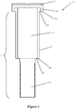
- Fig. 1 is a side view of a connector of the present invention.
- a connector 11, configured to be installed in an electronic device, has both the mechanical connecting function of the traditional connector and the function of electrically connecting two electronic parts.
- the connector 11 has a profile similar to a bolt, that is, the connector 11 has an end cap 3 and a cylindrical body 1.
- the cylindrical body 1 consists of a first section 1.1 and a second section 1.2.
- the first section 1.1 is formed between the end cap 3 and the second section 1.2, the end cap 3 has a diameter bigger than that of the first section 1.1, and the first section 1.1 has a diameter bigger than that of the second section 1.2.
- the connector 11 further has an insulator 2 formed circumferentially in one piece on the first section 1.1.
- an end surface of the end cap 3 facing the first section 1.1 is a first electrical contact surface A1
- an end surface connecting the first section 1.1 and the second section 1.2 is a second electrical contact surface A2.
- the first electrical contact surface A1 can be located in the same plane as a top surface of the insulator 2 facing the end cap 3.
- the end cap 3 preferably has an annular flange 3.1 separated radially from the first section 1.1, and an end surface of the annular flange 3.1 facing the first section 1.1 is the first electrical contact surface A1.
- An annular accommodating cavity is defined between the annular flange 3.1 and the first section 1.1 so that one end of the insulator 2 is accommodated fitly in the accommodating cavity.
- the first electrical contact surface A1 is the end surface of the annular flange 3.1, which is favorable for precisely contacting the first electrical contact surface A1 with a connecting region on parts in need of the electrical connection, and the first section 1.1 and this connecting region are electrically separated.
- an end surface connecting the first section 1.1 to the second section 1.2 is used as the second electrical contact surface A2 in the present embodiment.
- the first electrical contact surface A1 and a first end surface A3 of the insulator 2 extending beyond the accommodating cavity are configured to be in same level, and the second electrical contact surface A2 and a second end surface A4 of the insulator are in same level.
- the insulator 2 can be molded in one piece with the first section 1.1 through technologies such as insertion-injection or injection molding.
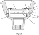
- Fig. 2 is a sectional view of an illuminating device of the present invention.
- the illuminating device comprises a circuit board 12, a heat sink 13, a driver 14, a driver housing 15 and a connector 11.
- the connector 11 mechanically connecting the parts above together in a screwing manner; moreover, the connector 11 realizes the electrical connection between the circuit board 12 and the driver 14 by using first and second electrical contact surfaces A1, A2.
- a second section 1.2 of the connector 11 is at least partially fixed in the driver housing 15.
- a first section of the connector 11 enclosed by an insulator 2 extends through the heat sink 13; the first electrical contact surface A1, i.e. annular end surface of an end cap 3 facing the first section 1.1 contacts a connecting region of the circuit board 12; the second electrical contact surface A2, i.e. an end surface connecting the first section 1.1 and the second section 1.2 contacts a connecting region of the driver 14. Therefore, the connector 11 merely electrically connects the circuit board 12 and the driver 14, and by means of the insulator 2, it is assured that a conductive portion of the connector 11 will not electrically contact the heat sink 13, thereby the short circuit is avoided.
Landscapes
- Engineering & Computer Science (AREA)
- General Engineering & Computer Science (AREA)
- Non-Portable Lighting Devices Or Systems Thereof (AREA)
- Arrangement Of Elements, Cooling, Sealing, Or The Like Of Lighting Devices (AREA)
- Connector Housings Or Holding Contact Members (AREA)
- Coupling Device And Connection With Printed Circuit (AREA)
Description
- The present invention relates to a connector for electronic device, an electronic device having the connector and an illuminating device configured to comprise the electronic device.
- With the development of science and technology, various electronic devices become an indispensable part in people's life. A common electronic device, particularly a high-power electronic device, comprises a circuit board, a heat sink, especially a metal heat sink, for cooling the circuit board, and a driver for driving the circuit board to operate. During assembling, the circuit board and the driver need to be electrically connected so as to supply power to components on the circuit board. Moreover, for the sake of good heat dissipating effects, the circuit board and the driver also need to be insulatedly and mechanically connected, for instance, the heat sink is arranged between the circuit board and the driver.
- In the prior art, the circuit board and the driver often should be independently connected by using, for instance, electrical lead or electrical connector, and the heat sink is fixed on a part to be cooled by additionally using, for instance, an adhesive paste or a buckle structure. In such a traditional assembling manner, not only electrical connection and mechanical connection need to be simultaneously performed, but also the process is quite complex and costly. When the adhesive paste is used for mechanical connection, adverse influences also may be exerted on the effect of the mechanical connection due to too high temperature of the heat sink. When the mechanical connection is performed by using, for instance, the buckle structure, since the buckle structure usually cannot be re-opened, it is inconvenient for the maintenance of the electronic device.
-
DE 43 10 440 A1 discloses a low-voltage lighting device comprising cylindrical connectors. - In order to solve the above problems, the present invention provides a connector for electronic device. The electrical connection and insulated mechanical connection can be simultaneously realized by using the connector; moreover, the connector has a simple structure and is easily installed and disassembled.
- A connector for electronic device is provided according to
claim 1 of the present invention, comprising a cylindrical body and an end cap formed at one end of the cylindrical body that comprises a first section and a second section, wherein the first section is formed between the end cap and the second section, the end cap has a diameter bigger than that of the first section, and the first section has a diameter bigger than that of the second section, and a circumferential wall of the second section at least partially has threads, and the connector further comprises an insulator circumferentially
formed in one piece on the first section, the end cap comprises a first electrical contact surface on an end surface facing the first section, and the first section comprises a second electrical contact surface on an end surface facing the second section. - The concept of the present invention lies in using the conductivity and the thread structure of the connector made often of a metal to simultaneously realize the electrical connection and the mechanical connection. By taking the insulation requirement in mechanical connection into particular consideration, the connector further has the insulator formed in one piece. The insulator merely encloses the first section in a circumferential direction to assure the insulation property of the first section, and also assure two end surfaces of the connector, as the first and second electrical contact surfaces, not to be covered by the insulator. The connector configured in such a manner, when making connection in an electronic device, can electrically connect two electronic parts to be connected by using the first and second electrical contact surfaces; moreover, by means of the insulator, the electrical insulation is realized with other electronic parts that need no electrical connection. Therefore, a reliable electrical connection and mechanical connection is guaranteed in the electronic device.
- In one preferred solution of the present invention, the insulator is molded on the first section through an insert-injection technology. Thus, the insulator and the connector are formed in one piece. The insulator and the connector also can be fabricated in one piece through injection molding or other similar technologies.
- In one preferred solution of the present invention, the end cap has an annular flange radially separated from the first section, and an end surface of the annular flange facing the first section is the first electrical contact surface. The size of the interval between the annular flange and the first section is designed to match a position of a region to be contacted of the circuit board. Accordingly, the first electrical contact surface can be enabled to precisely electrically contact a predetermined region of parts in need of electrical connection, such as a connecting region of the circuit board. In another embodiment, the end cap also may not have the annular flange radially separated from the cylindrical body, and the insulator is merely against part of region of a lower surface of the end cap, and the other regions of the lower surface of the end cap are configured to be the first electrical contact surface.
- In one preferred solution of the present invention, the annular flange and the first section define an annular accommodating cavity, in which one end of the insulator is accommodated fitly. As a result, it is assured that only the first electrical contact surface of the connector contacts the connecting region of parts in need of electrical connection, but the first section and the connecting region are electrically insulated.
- In one preferred solution of the present invention, a first end surface of the insulator close to the end cap and the first electrical contact surface are in same level. Preferably, the second end surface of the insulator away from the end cap and the second electrical contact surface are in same level. Such configuration simplifies the fabrication and installation of the connector.
- In one preferred solution of the present invention, the cylindrical body and the end cap are made of a conductive material. Preferably, the cylindrical body and the end cap are made of copper. Of course, the cylindrical body and the end cap also can be made of other materials such as A1 that have favorable conductive performances.
- In addition, the present invention further provides an electronic device comprising at least one connector described above, and comprising a circuit board, a driver housing accommodating a driver and a heat sink.
- In one preferred solution of the present invention, the connector connects the circuit board, the heat sink, the driver and the driver housing in sequence, wherein a first section of the connector enclosed by an insulator extends through the heat sink, a first electrical contact surface of the connector and the circuit board are electrically connected, a second electrical contact surface of the connector and the driver are electrically connected, and the second section is inserted into the driver housing. On one hand, the connector electrically connects the circuit board and the driver by using the first and second electrical contact surfaces; and on the other hand, in order to avoid risks, such as short circuit, of the connector and the heat sink in a fixed state, due to electrical contact, part of the connector with the insulator, i.e., the first section circumferentially enclosed by the insulator, particularly runs through the region where the electrical contact is not needed. Therefore, the connector simply and releasably mechanically connects the heat sink and the driver housing together.
- Another object of the present invention is accomplished via an illuminating device comprising the electronic device of the above type and a light source, wherein the light source is installed on a circuit board of the electronic device.
- The accompanying drawings constitute a part of the present Description and are used to provide further understanding of the present invention. Such accompanying drawings illustrate the embodiments of the present invention and are used to describe the principles of the present invention together with the Description. In the accompanying drawings the same components are represented by the same reference numbers. As shown in the drawings:
-
Fig. 1 is a side view of a connector of the present invention; and -
Fig. 2 is a sectional view of an illuminating device of the present invention. -
Fig. 1 is a side view of a connector of the present invention. Aconnector 11, configured to be installed in an electronic device, has both the mechanical connecting function of the traditional connector and the function of electrically connecting two electronic parts. Theconnector 11 has a profile similar to a bolt, that is, theconnector 11 has anend cap 3 and acylindrical body 1. Thecylindrical body 1 consists of a first section 1.1 and a second section 1.2. The first section 1.1 is formed between theend cap 3 and the second section 1.2, theend cap 3 has a diameter bigger than that of the first section 1.1, and the first section 1.1 has a diameter bigger than that of the second section 1.2. Besides, theconnector 11 further has aninsulator 2 formed circumferentially in one piece on the first section 1.1. - As the diameters of respective sections of the
connector 11 are reduced in sequence, an end surface of theend cap 3 facing the first section 1.1 is a first electrical contact surface A1, and an end surface connecting the first section 1.1 and the second section 1.2 is a second electrical contact surface A2. By contacting the first and second electrical contact surfaces A1, A2 with different electronic parts, respectively, a reliable electrical connection between the electronic parts can be realized. Moreover, theinsulator 2 assures the first section 1.1 that can be conductive not to electrically contact the electronic parts. Besides, a circumferential wall of the second section 1.2 at least partially has threads so as to realize a mechanical connecting function similar to that of the bolt. - In one preferred embodiment, the first electrical contact surface A1 can be located in the same plane as a top surface of the
insulator 2 facing theend cap 3. In the embodiment shown inFig. 1 , theend cap 3 preferably has an annular flange 3.1 separated radially from the first section 1.1, and an end surface of the annular flange 3.1 facing the first section 1.1 is the first electrical contact surface A1. An annular accommodating cavity is defined between the annular flange 3.1 and the first section 1.1 so that one end of theinsulator 2 is accommodated fitly in the accommodating cavity. The first electrical contact surface A1 is the end surface of the annular flange 3.1, which is favorable for precisely contacting the first electrical contact surface A1 with a connecting region on parts in need of the electrical connection, and the first section 1.1 and this connecting region are electrically separated. In addition, an end surface connecting the first section 1.1 to the second section 1.2 is used as the second electrical contact surface A2 in the present embodiment. For the sake of convenient fabrication and installation, the first electrical contact surface A1 and a first end surface A3 of theinsulator 2 extending beyond the accommodating cavity are configured to be in same level, and the second electrical contact surface A2 and a second end surface A4 of the insulator are in same level. - In the
connector 11 of the present invention, theinsulator 2 can be molded in one piece with the first section 1.1 through technologies such as insertion-injection or injection molding. -
Fig. 2 is a sectional view of an illuminating device of the present invention. The illuminating device comprises acircuit board 12, aheat sink 13, adriver 14, adriver housing 15 and aconnector 11. Theconnector 11 mechanically connecting the parts above together in a screwing manner; moreover, theconnector 11 realizes the electrical connection between thecircuit board 12 and thedriver 14 by using first and second electrical contact surfaces A1, A2. - It can be seen clearly from
Fig. 2 that in a connection state, a second section 1.2 of theconnector 11 is at least partially fixed in thedriver housing 15. A first section of theconnector 11 enclosed by aninsulator 2 extends through theheat sink 13; the first electrical contact surface A1, i.e. annular end surface of anend cap 3 facing the first section 1.1 contacts a connecting region of thecircuit board 12; the second electrical contact surface A2, i.e. an end surface connecting the first section 1.1 and the second section 1.2 contacts a connecting region of thedriver 14. Therefore, theconnector 11 merely electrically connects thecircuit board 12 and thedriver 14, and by means of theinsulator 2, it is assured that a conductive portion of theconnector 11 will not electrically contact theheat sink 13, thereby the short circuit is avoided. - The above is merely preferred embodiments of the present invention but not to limit the present invention. For the person skilled in the art, the present invention may have various alterations and changes. Any alterations within the principle of the present invention should be covered in the protection scope of the appended claims.
-
- 1
- cylindrical body
- 1.1
- first section
- 1.2
- second section
- 2
- insulator
- 3
- end cap
- 11
- connector
- 12
- circuit board
- 13
- heat sink
- 14
- driver
- 15
- driver housing
- A1
- first electrical contact surface
- A2
- second electrical contact surface
- A3
- first end surface
- A4
- second end surface
Claims (11)
- A connector (11) for an electronic device, comprising a cylindrical body (1) and an end cap (3) formed at one end of the cylindrical body (1) that comprises a first section (1.1) and a second section (1.2), wherein the first section (1.1) is formed between the end cap (3) and the second section (1.2), the end cap (3) has a diameter bigger than that of the first section (1.1), and the first section (1.1) has a diameter bigger than that of the second section (1.2), and a circumferential wall of the second section (1.2) at least partially has threads, wherein the end cap (3) comprises a first electrical contact surface (A1) on an end surface facing the first section (1.1), and the first section (1.1) comprises a second electrical contact surface (A2) on an end surface facing the second section (1.2), characterized by further comprising an insulator (2) circumferentially formed in one piece on the first section (1.1), wherein the first electrical contact surface (A1) and the second electrical contact surface (A2) are not covered by the insulator (2).
- The connector (11) according to Claim 1, characterized in that the insulator (2) is molded on the first section (1.1) through an insert-injection technology.
- The connector (11) according to Claim 1 or 2, characterized in that the end cap (3) has an annular flange (3.1) radially separated from the first section (1.1), and an end surface of the annular flange (3.1) facing the first section (1.1) is the first electrical contact surface (A1).
- The connector (11) according to Claim 3, characterized in that the annular flange (3.1) and the first section (1.1) define an annular accommodating cavity, in which one end of the insulator (2) is accommodated fitly.
- The connector (11) according to Claim 4, characterized in that a first end surface (A3) of the insulator (2) close to the end cap (3) and the first electrical contact surface (A1) are in same level.
- The connector (11) according to Claim 4, characterized in that a second end surface (A4) of the insulator (2) away from the end cap (3) and the second electrical contact surface (A2) are in same level.
- The connector (11) according to Claim 1 or 2, characterized in that the cylindrical body (1) and the end cap (3) are made of a conductive material.
- The connector (11) according to Claim 7, characterized in that the cylindrical body (1) and the end cap (3) are made of copper.
- An electronic device, comprising a circuit board (12), a driver housing (15) accommodating a driver (14) and a heat sink (13), characterized in that the electronic device further comprises at least one connector (11) according to any one of Claims 1-8.
- The electronic device according to Claim 9, characterized in that the connector (11) connects the circuit board (12), the heat sink (13), the driver (14) and the driver housing (15) in sequence, wherein a first section (1.1) of the connector (11) enclosed by an insulator (2) extends through the heat sink (13), a first electrical contact surface (A1) of the connector (11) and the circuit board (12) are electrically connected, a second electrical contact surface (A2) of the connector (11) and the driver (14) are electrically connected, and the second section (1.2) is inserted into the driver housing (15).
- An illuminating device, characterized by comprising the electronic device according to Claim 9 or 10 and a light source mounted on the circuit board (12).
Applications Claiming Priority (2)
| Application Number | Priority Date | Filing Date | Title |
|---|---|---|---|
| CN201210006329.XA CN103199370B (en) | 2012-01-10 | 2012-01-10 | Connector, the electronic installation with this connector and illuminator |
| PCT/EP2012/075748 WO2013104490A1 (en) | 2012-01-10 | 2012-12-17 | Connector, electronic device and illuminating device having the connector |
Publications (3)
| Publication Number | Publication Date |
|---|---|
| EP2803114A1 EP2803114A1 (en) | 2014-11-19 |
| EP2803114B1 true EP2803114B1 (en) | 2017-05-10 |
| EP2803114B8 EP2803114B8 (en) | 2017-08-02 |
Family
ID=47469971
Family Applications (1)
| Application Number | Title | Priority Date | Filing Date |
|---|---|---|---|
| EP12808794.7A Not-in-force EP2803114B8 (en) | 2012-01-10 | 2012-12-17 | Connector, electronic device and illuminating device having the connector |
Country Status (4)
| Country | Link |
|---|---|
| US (1) | US9400097B2 (en) |
| EP (1) | EP2803114B8 (en) |
| CN (1) | CN103199370B (en) |
| WO (1) | WO2013104490A1 (en) |
Cited By (1)
| Publication number | Priority date | Publication date | Assignee | Title |
|---|---|---|---|---|
| DE102017113872A1 (en) * | 2017-06-22 | 2018-12-27 | Trilux Gmbh & Co. Kg | LED array |
Families Citing this family (3)
| Publication number | Priority date | Publication date | Assignee | Title |
|---|---|---|---|---|
| CN104916942A (en) * | 2014-03-14 | 2015-09-16 | 鸿富锦精密工业(武汉)有限公司 | Connector and pin |
| CN108037435A (en) * | 2017-12-08 | 2018-05-15 | 贵州振华风光半导体有限公司 | The direct-connected device of ic component assembly type array |
| CN114270631B (en) * | 2019-09-11 | 2024-01-23 | 西门子股份公司 | Circuit board connection structure |
Family Cites Families (14)
| Publication number | Priority date | Publication date | Assignee | Title |
|---|---|---|---|---|
| DE3700661A1 (en) | 1986-11-05 | 1988-07-21 | Hagemeyer Georg Maria | Lighting device |
| US4760495A (en) * | 1987-04-16 | 1988-07-26 | Prime Computer Inc. | Stand-off device |
| GB8808212D0 (en) | 1988-04-08 | 1988-05-11 | Syrinx Innovations | Forming mechanical & electrical connections printed circuit board |
| WO1993007659A1 (en) * | 1991-10-09 | 1993-04-15 | Ifax Corporation | Direct integrated circuit interconnection system |
| JPH05259603A (en) * | 1992-03-13 | 1993-10-08 | Sony Corp | Supporting member for printed wiring board and method of stacking printed wiring board |
| DE4310440A1 (en) * | 1992-03-31 | 1994-02-17 | Guss Peter | Low voltage illuminating device - has two terminal lamp socket electrically and mechanically connected in flat carrier strip. |
| JPH0918109A (en) * | 1995-06-30 | 1997-01-17 | Nippon Seiki Co Ltd | Fixing structure for printed board |
| DE60329478D1 (en) * | 2002-03-20 | 2009-11-12 | Andrew Llc | PINS AND SOCKETS FOR INTERMEDIATING TWO PCBS, AND METHOD FOR MOUNTING INTO A PCB |
| US6787999B2 (en) * | 2002-10-03 | 2004-09-07 | Gelcore, Llc | LED-based modular lamp |
| US7025604B2 (en) * | 2003-03-31 | 2006-04-11 | Astec International Limited | High current output pin |
| DE202008016800U1 (en) * | 2008-12-19 | 2010-05-27 | Weidmüller Interface GmbH & Co. KG | Connecting device for flat conductor |
| US8186852B2 (en) * | 2009-06-24 | 2012-05-29 | Elumigen Llc | Opto-thermal solution for multi-utility solid state lighting device using conic section geometries |
| US8342733B2 (en) * | 2009-12-14 | 2013-01-01 | Tyco Electronics Corporation | LED lighting assemblies |
| CN201925782U (en) * | 2011-01-24 | 2011-08-10 | 深圳市卡比特半导体照明有限公司 | LED (light-emitting diode) lamp |
-
2012
- 2012-01-10 CN CN201210006329.XA patent/CN103199370B/en not_active Expired - Fee Related
- 2012-12-17 US US14/370,969 patent/US9400097B2/en active Active
- 2012-12-17 EP EP12808794.7A patent/EP2803114B8/en not_active Not-in-force
- 2012-12-17 WO PCT/EP2012/075748 patent/WO2013104490A1/en active Application Filing
Non-Patent Citations (1)
| Title |
|---|
| None * |
Cited By (1)
| Publication number | Priority date | Publication date | Assignee | Title |
|---|---|---|---|---|
| DE102017113872A1 (en) * | 2017-06-22 | 2018-12-27 | Trilux Gmbh & Co. Kg | LED array |
Also Published As
| Publication number | Publication date |
|---|---|
| EP2803114B8 (en) | 2017-08-02 |
| CN103199370B (en) | 2016-09-28 |
| WO2013104490A1 (en) | 2013-07-18 |
| CN103199370A (en) | 2013-07-10 |
| US9400097B2 (en) | 2016-07-26 |
| EP2803114A1 (en) | 2014-11-19 |
| US20140347869A1 (en) | 2014-11-27 |
Similar Documents
| Publication | Publication Date | Title |
|---|---|---|
| US8696168B2 (en) | Illumination device | |
| US9464765B2 (en) | LED lighting apparatus | |
| KR101398701B1 (en) | Led device, manufacturing method thereof, and light-emitting device | |
| EP2579392B1 (en) | Connector and illumination device | |
| US9373922B2 (en) | LED illumination device with edge connector | |
| EP2937628A1 (en) | Electric connecting piece and led lamp using same | |
| EP3098506B1 (en) | Electrical connection structure of lamp cap | |
| EP2803114B1 (en) | Connector, electronic device and illuminating device having the connector | |
| EP3273159B1 (en) | Integrated electric connection structure for led lamp | |
| US20150323139A1 (en) | Wide-angle led bulb | |
| US20200248899A1 (en) | Integrated electrical connector device structure of led light | |
| EP2802812B1 (en) | Illuminating device and manufacturing method thereof | |
| WO2013060510A1 (en) | An led illuminating device | |
| US10775007B2 (en) | Split type downlight apparatus | |
| CN205065391U (en) | Luminous means | |
| JP2016025088A (en) | Light-emitting diode bulb | |
| CN203731324U (en) | Electric connection structure for lamp holder | |
| CN102278617A (en) | Lamp | |
| TW201528563A (en) | Led module with ceramic substrate and driver module for a network voltage | |
| JP2010287888A (en) | Contact device of control connection for power semiconductor component | |
| CN221176722U (en) | Alternating current connector and LED box with same | |
| JP2013010290A (en) | Method of manufacturing bulb lamp housing | |
| JP5703634B2 (en) | Electrical equipment | |
| JP2012043585A (en) | Bulb-type led lamp | |
| JP3192284U (en) | LED tube lamp end assembly structure |
Legal Events
| Date | Code | Title | Description |
|---|---|---|---|
| PUAI | Public reference made under article 153(3) epc to a published international application that has entered the european phase |
Free format text: ORIGINAL CODE: 0009012 |
|
| 17P | Request for examination filed |
Effective date: 20140811 |
|
| AK | Designated contracting states |
Kind code of ref document: A1 Designated state(s): AL AT BE BG CH CY CZ DE DK EE ES FI FR GB GR HR HU IE IS IT LI LT LU LV MC MK MT NL NO PL PT RO RS SE SI SK SM TR |
|
| DAX | Request for extension of the european patent (deleted) | ||
| 17Q | First examination report despatched |
Effective date: 20160728 |
|
| GRAP | Despatch of communication of intention to grant a patent |
Free format text: ORIGINAL CODE: EPIDOSNIGR1 |
|
| RIC1 | Information provided on ipc code assigned before grant |
Ipc: H05K 5/00 20060101ALI20160929BHEP Ipc: H01R 12/73 20110101ALI20160929BHEP Ipc: F21V 29/70 20150101ALI20160929BHEP Ipc: F21V 19/00 20060101ALI20160929BHEP Ipc: F21V 23/06 20060101ALI20160929BHEP Ipc: H01R 13/512 20060101ALI20160929BHEP Ipc: F21V 23/00 20150101ALI20160929BHEP Ipc: H01R 12/71 20110101ALN20160929BHEP Ipc: H01R 12/52 20110101AFI20160929BHEP |
|
| INTG | Intention to grant announced |
Effective date: 20161021 |
|
| GRAS | Grant fee paid |
Free format text: ORIGINAL CODE: EPIDOSNIGR3 |
|
| GRAJ | Information related to disapproval of communication of intention to grant by the applicant or resumption of examination proceedings by the epo deleted |
Free format text: ORIGINAL CODE: EPIDOSDIGR1 |
|
| GRAL | Information related to payment of fee for publishing/printing deleted |
Free format text: ORIGINAL CODE: EPIDOSDIGR3 |
|
| INTC | Intention to grant announced (deleted) | ||
| GRAR | Information related to intention to grant a patent recorded |
Free format text: ORIGINAL CODE: EPIDOSNIGR71 |
|
| RIC1 | Information provided on ipc code assigned before grant |
Ipc: H01R 12/73 20110101ALI20170224BHEP Ipc: H01R 12/71 20110101ALN20170224BHEP Ipc: H01R 13/512 20060101ALI20170224BHEP Ipc: F21V 29/70 20150101ALI20170224BHEP Ipc: H01R 12/52 20110101AFI20170224BHEP Ipc: F21V 23/06 20060101ALI20170224BHEP Ipc: F21V 19/00 20060101ALI20170224BHEP Ipc: H05K 5/00 20060101ALI20170224BHEP Ipc: F21V 23/00 20150101ALI20170224BHEP |
|
| GRAA | (expected) grant |
Free format text: ORIGINAL CODE: 0009210 |
|
| AK | Designated contracting states |
Kind code of ref document: B1 Designated state(s): AL AT BE BG CH CY CZ DE DK EE ES FI FR GB GR HR HU IE IS IT LI LT LU LV MC MK MT NL NO PL PT RO RS SE SI SK SM TR |
|
| INTG | Intention to grant announced |
Effective date: 20170403 |
|
| REG | Reference to a national code |
Ref country code: GB Ref legal event code: FG4D |
|
| REG | Reference to a national code |
Ref country code: AT Ref legal event code: REF Ref document number: 893219 Country of ref document: AT Kind code of ref document: T Effective date: 20170515 Ref country code: CH Ref legal event code: EP |
|
| REG | Reference to a national code |
Ref country code: IE Ref legal event code: FG4D |
|
| RAP2 | Party data changed (patent owner data changed or rights of a patent transferred) |
Owner name: LEDVANCE GMBH |
|
| REG | Reference to a national code |
Ref country code: DE Ref legal event code: R096 Ref document number: 602012032334 Country of ref document: DE |
|
| REG | Reference to a national code |
Ref country code: NL Ref legal event code: MP Effective date: 20170510 |
|
| REG | Reference to a national code |
Ref country code: LT Ref legal event code: MG4D |
|
| REG | Reference to a national code |
Ref country code: AT Ref legal event code: MK05 Ref document number: 893219 Country of ref document: AT Kind code of ref document: T Effective date: 20170510 |
|
| PG25 | Lapsed in a contracting state [announced via postgrant information from national office to epo] |
Ref country code: FI Free format text: LAPSE BECAUSE OF FAILURE TO SUBMIT A TRANSLATION OF THE DESCRIPTION OR TO PAY THE FEE WITHIN THE PRESCRIBED TIME-LIMIT Effective date: 20170510 Ref country code: GR Free format text: LAPSE BECAUSE OF FAILURE TO SUBMIT A TRANSLATION OF THE DESCRIPTION OR TO PAY THE FEE WITHIN THE PRESCRIBED TIME-LIMIT Effective date: 20170811 Ref country code: HR Free format text: LAPSE BECAUSE OF FAILURE TO SUBMIT A TRANSLATION OF THE DESCRIPTION OR TO PAY THE FEE WITHIN THE PRESCRIBED TIME-LIMIT Effective date: 20170510 Ref country code: LT Free format text: LAPSE BECAUSE OF FAILURE TO SUBMIT A TRANSLATION OF THE DESCRIPTION OR TO PAY THE FEE WITHIN THE PRESCRIBED TIME-LIMIT Effective date: 20170510 Ref country code: NO Free format text: LAPSE BECAUSE OF FAILURE TO SUBMIT A TRANSLATION OF THE DESCRIPTION OR TO PAY THE FEE WITHIN THE PRESCRIBED TIME-LIMIT Effective date: 20170810 Ref country code: AT Free format text: LAPSE BECAUSE OF FAILURE TO SUBMIT A TRANSLATION OF THE DESCRIPTION OR TO PAY THE FEE WITHIN THE PRESCRIBED TIME-LIMIT Effective date: 20170510 |
|
| PG25 | Lapsed in a contracting state [announced via postgrant information from national office to epo] |
Ref country code: BG Free format text: LAPSE BECAUSE OF FAILURE TO SUBMIT A TRANSLATION OF THE DESCRIPTION OR TO PAY THE FEE WITHIN THE PRESCRIBED TIME-LIMIT Effective date: 20170810 Ref country code: NL Free format text: LAPSE BECAUSE OF FAILURE TO SUBMIT A TRANSLATION OF THE DESCRIPTION OR TO PAY THE FEE WITHIN THE PRESCRIBED TIME-LIMIT Effective date: 20170510 Ref country code: IS Free format text: LAPSE BECAUSE OF FAILURE TO SUBMIT A TRANSLATION OF THE DESCRIPTION OR TO PAY THE FEE WITHIN THE PRESCRIBED TIME-LIMIT Effective date: 20170910 Ref country code: RS Free format text: LAPSE BECAUSE OF FAILURE TO SUBMIT A TRANSLATION OF THE DESCRIPTION OR TO PAY THE FEE WITHIN THE PRESCRIBED TIME-LIMIT Effective date: 20170510 Ref country code: PL Free format text: LAPSE BECAUSE OF FAILURE TO SUBMIT A TRANSLATION OF THE DESCRIPTION OR TO PAY THE FEE WITHIN THE PRESCRIBED TIME-LIMIT Effective date: 20170510 Ref country code: SE Free format text: LAPSE BECAUSE OF FAILURE TO SUBMIT A TRANSLATION OF THE DESCRIPTION OR TO PAY THE FEE WITHIN THE PRESCRIBED TIME-LIMIT Effective date: 20170510 Ref country code: LV Free format text: LAPSE BECAUSE OF FAILURE TO SUBMIT A TRANSLATION OF THE DESCRIPTION OR TO PAY THE FEE WITHIN THE PRESCRIBED TIME-LIMIT Effective date: 20170510 |
|
| REG | Reference to a national code |
Ref country code: FR Ref legal event code: PLFP Year of fee payment: 6 |
|
| PG25 | Lapsed in a contracting state [announced via postgrant information from national office to epo] |
Ref country code: SK Free format text: LAPSE BECAUSE OF FAILURE TO SUBMIT A TRANSLATION OF THE DESCRIPTION OR TO PAY THE FEE WITHIN THE PRESCRIBED TIME-LIMIT Effective date: 20170510 Ref country code: EE Free format text: LAPSE BECAUSE OF FAILURE TO SUBMIT A TRANSLATION OF THE DESCRIPTION OR TO PAY THE FEE WITHIN THE PRESCRIBED TIME-LIMIT Effective date: 20170510 Ref country code: RO Free format text: LAPSE BECAUSE OF FAILURE TO SUBMIT A TRANSLATION OF THE DESCRIPTION OR TO PAY THE FEE WITHIN THE PRESCRIBED TIME-LIMIT Effective date: 20170510 Ref country code: CZ Free format text: LAPSE BECAUSE OF FAILURE TO SUBMIT A TRANSLATION OF THE DESCRIPTION OR TO PAY THE FEE WITHIN THE PRESCRIBED TIME-LIMIT Effective date: 20170510 Ref country code: DK Free format text: LAPSE BECAUSE OF FAILURE TO SUBMIT A TRANSLATION OF THE DESCRIPTION OR TO PAY THE FEE WITHIN THE PRESCRIBED TIME-LIMIT Effective date: 20170510 |
|
| REG | Reference to a national code |
Ref country code: DE Ref legal event code: R097 Ref document number: 602012032334 Country of ref document: DE |
|
| PG25 | Lapsed in a contracting state [announced via postgrant information from national office to epo] |
Ref country code: SM Free format text: LAPSE BECAUSE OF FAILURE TO SUBMIT A TRANSLATION OF THE DESCRIPTION OR TO PAY THE FEE WITHIN THE PRESCRIBED TIME-LIMIT Effective date: 20170510 Ref country code: IT Free format text: LAPSE BECAUSE OF FAILURE TO SUBMIT A TRANSLATION OF THE DESCRIPTION OR TO PAY THE FEE WITHIN THE PRESCRIBED TIME-LIMIT Effective date: 20170510 |
|
| PLBE | No opposition filed within time limit |
Free format text: ORIGINAL CODE: 0009261 |
|
| STAA | Information on the status of an ep patent application or granted ep patent |
Free format text: STATUS: NO OPPOSITION FILED WITHIN TIME LIMIT |
|
| 26N | No opposition filed |
Effective date: 20180213 |
|
| PG25 | Lapsed in a contracting state [announced via postgrant information from national office to epo] |
Ref country code: SI Free format text: LAPSE BECAUSE OF FAILURE TO SUBMIT A TRANSLATION OF THE DESCRIPTION OR TO PAY THE FEE WITHIN THE PRESCRIBED TIME-LIMIT Effective date: 20170510 |
|
| REG | Reference to a national code |
Ref country code: CH Ref legal event code: PL |
|
| REG | Reference to a national code |
Ref country code: IE Ref legal event code: MM4A |
|
| PG25 | Lapsed in a contracting state [announced via postgrant information from national office to epo] |
Ref country code: MT Free format text: LAPSE BECAUSE OF NON-PAYMENT OF DUE FEES Effective date: 20171217 Ref country code: LU Free format text: LAPSE BECAUSE OF NON-PAYMENT OF DUE FEES Effective date: 20171217 |
|
| REG | Reference to a national code |
Ref country code: BE Ref legal event code: MM Effective date: 20171231 |
|
| PG25 | Lapsed in a contracting state [announced via postgrant information from national office to epo] |
Ref country code: IE Free format text: LAPSE BECAUSE OF NON-PAYMENT OF DUE FEES Effective date: 20171217 |
|
| PG25 | Lapsed in a contracting state [announced via postgrant information from national office to epo] |
Ref country code: BE Free format text: LAPSE BECAUSE OF NON-PAYMENT OF DUE FEES Effective date: 20171231 Ref country code: CH Free format text: LAPSE BECAUSE OF NON-PAYMENT OF DUE FEES Effective date: 20171231 Ref country code: LI Free format text: LAPSE BECAUSE OF NON-PAYMENT OF DUE FEES Effective date: 20171231 |
|
| PG25 | Lapsed in a contracting state [announced via postgrant information from national office to epo] |
Ref country code: HU Free format text: LAPSE BECAUSE OF FAILURE TO SUBMIT A TRANSLATION OF THE DESCRIPTION OR TO PAY THE FEE WITHIN THE PRESCRIBED TIME-LIMIT; INVALID AB INITIO Effective date: 20121217 Ref country code: MC Free format text: LAPSE BECAUSE OF FAILURE TO SUBMIT A TRANSLATION OF THE DESCRIPTION OR TO PAY THE FEE WITHIN THE PRESCRIBED TIME-LIMIT Effective date: 20170510 |
|
| PG25 | Lapsed in a contracting state [announced via postgrant information from national office to epo] |
Ref country code: ES Free format text: LAPSE BECAUSE OF NON-PAYMENT OF DUE FEES Effective date: 20170510 |
|
| PG25 | Lapsed in a contracting state [announced via postgrant information from national office to epo] |
Ref country code: CY Free format text: LAPSE BECAUSE OF FAILURE TO SUBMIT A TRANSLATION OF THE DESCRIPTION OR TO PAY THE FEE WITHIN THE PRESCRIBED TIME-LIMIT Effective date: 20170510 |
|
| PG25 | Lapsed in a contracting state [announced via postgrant information from national office to epo] |
Ref country code: MK Free format text: LAPSE BECAUSE OF FAILURE TO SUBMIT A TRANSLATION OF THE DESCRIPTION OR TO PAY THE FEE WITHIN THE PRESCRIBED TIME-LIMIT Effective date: 20170510 |
|
| PGFP | Annual fee paid to national office [announced via postgrant information from national office to epo] |
Ref country code: FR Payment date: 20191224 Year of fee payment: 8 |
|
| PG25 | Lapsed in a contracting state [announced via postgrant information from national office to epo] |
Ref country code: TR Free format text: LAPSE BECAUSE OF FAILURE TO SUBMIT A TRANSLATION OF THE DESCRIPTION OR TO PAY THE FEE WITHIN THE PRESCRIBED TIME-LIMIT Effective date: 20170510 |
|
| PGFP | Annual fee paid to national office [announced via postgrant information from national office to epo] |
Ref country code: DE Payment date: 20200227 Year of fee payment: 8 Ref country code: GB Payment date: 20191226 Year of fee payment: 8 |
|
| PG25 | Lapsed in a contracting state [announced via postgrant information from national office to epo] |
Ref country code: PT Free format text: LAPSE BECAUSE OF FAILURE TO SUBMIT A TRANSLATION OF THE DESCRIPTION OR TO PAY THE FEE WITHIN THE PRESCRIBED TIME-LIMIT Effective date: 20170510 |
|
| PG25 | Lapsed in a contracting state [announced via postgrant information from national office to epo] |
Ref country code: AL Free format text: LAPSE BECAUSE OF FAILURE TO SUBMIT A TRANSLATION OF THE DESCRIPTION OR TO PAY THE FEE WITHIN THE PRESCRIBED TIME-LIMIT Effective date: 20170510 |
|
| REG | Reference to a national code |
Ref country code: DE Ref legal event code: R119 Ref document number: 602012032334 Country of ref document: DE |
|
| GBPC | Gb: european patent ceased through non-payment of renewal fee |
Effective date: 20201217 |
|
| PG25 | Lapsed in a contracting state [announced via postgrant information from national office to epo] |
Ref country code: FR Free format text: LAPSE BECAUSE OF NON-PAYMENT OF DUE FEES Effective date: 20201231 |
|
| PG25 | Lapsed in a contracting state [announced via postgrant information from national office to epo] |
Ref country code: DE Free format text: LAPSE BECAUSE OF NON-PAYMENT OF DUE FEES Effective date: 20210701 Ref country code: GB Free format text: LAPSE BECAUSE OF NON-PAYMENT OF DUE FEES Effective date: 20201217 |