EP2803086B1 - Semiconductor devices - Google Patents
Semiconductor devices Download PDFInfo
- Publication number
- EP2803086B1 EP2803086B1 EP13701580.6A EP13701580A EP2803086B1 EP 2803086 B1 EP2803086 B1 EP 2803086B1 EP 13701580 A EP13701580 A EP 13701580A EP 2803086 B1 EP2803086 B1 EP 2803086B1
- Authority
- EP
- European Patent Office
- Prior art keywords
- interposer
- pitch
- semiconductor chip
- semiconductor device
- chip
- Prior art date
- Legal status (The legal status is an assumption and is not a legal conclusion. Google has not performed a legal analysis and makes no representation as to the accuracy of the status listed.)
- Active
Links
Images






Classifications
-
- H—ELECTRICITY
- H10—SEMICONDUCTOR DEVICES; ELECTRIC SOLID-STATE DEVICES NOT OTHERWISE PROVIDED FOR
- H10W—GENERIC PACKAGES, INTERCONNECTIONS, CONNECTORS OR OTHER CONSTRUCTIONAL DETAILS OF DEVICES COVERED BY CLASS H10
- H10W72/00—Interconnections or connectors in packages
- H10W72/071—Connecting or disconnecting
- H10W72/072—Connecting or disconnecting of bump connectors
-
- H—ELECTRICITY
- H10—SEMICONDUCTOR DEVICES; ELECTRIC SOLID-STATE DEVICES NOT OTHERWISE PROVIDED FOR
- H10W—GENERIC PACKAGES, INTERCONNECTIONS, CONNECTORS OR OTHER CONSTRUCTIONAL DETAILS OF DEVICES COVERED BY CLASS H10
- H10W70/00—Package substrates; Interposers; Redistribution layers [RDL]
- H10W70/01—Manufacture or treatment
- H10W70/05—Manufacture or treatment of insulating or insulated package substrates, or of interposers, or of redistribution layers
- H10W70/08—Manufacture or treatment of insulating or insulated package substrates, or of interposers, or of redistribution layers by depositing layers on the chip or wafer, e.g. "chip-first" RDLs
- H10W70/09—Manufacture or treatment of insulating or insulated package substrates, or of interposers, or of redistribution layers by depositing layers on the chip or wafer, e.g. "chip-first" RDLs extending onto an encapsulation that laterally surrounds the chip or wafer, e.g. fan-out wafer level package [FOWLP] RDLs
-
- H—ELECTRICITY
- H10—SEMICONDUCTOR DEVICES; ELECTRIC SOLID-STATE DEVICES NOT OTHERWISE PROVIDED FOR
- H10W—GENERIC PACKAGES, INTERCONNECTIONS, CONNECTORS OR OTHER CONSTRUCTIONAL DETAILS OF DEVICES COVERED BY CLASS H10
- H10W70/00—Package substrates; Interposers; Redistribution layers [RDL]
- H10W70/60—Insulating or insulated package substrates; Interposers; Redistribution layers
- H10W70/611—Insulating or insulated package substrates; Interposers; Redistribution layers for connecting multiple chips together
- H10W70/614—Insulating or insulated package substrates; Interposers; Redistribution layers for connecting multiple chips together the multiple chips being integrally enclosed
-
- H—ELECTRICITY
- H10—SEMICONDUCTOR DEVICES; ELECTRIC SOLID-STATE DEVICES NOT OTHERWISE PROVIDED FOR
- H10W—GENERIC PACKAGES, INTERCONNECTIONS, CONNECTORS OR OTHER CONSTRUCTIONAL DETAILS OF DEVICES COVERED BY CLASS H10
- H10W72/00—Interconnections or connectors in packages
- H10W72/01—Manufacture or treatment
- H10W72/0198—Manufacture or treatment batch processes
-
- H—ELECTRICITY
- H10—SEMICONDUCTOR DEVICES; ELECTRIC SOLID-STATE DEVICES NOT OTHERWISE PROVIDED FOR
- H10W—GENERIC PACKAGES, INTERCONNECTIONS, CONNECTORS OR OTHER CONSTRUCTIONAL DETAILS OF DEVICES COVERED BY CLASS H10
- H10W72/00—Interconnections or connectors in packages
- H10W72/20—Bump connectors, e.g. solder bumps or copper pillars; Dummy bumps; Thermal bumps
-
- H—ELECTRICITY
- H10—SEMICONDUCTOR DEVICES; ELECTRIC SOLID-STATE DEVICES NOT OTHERWISE PROVIDED FOR
- H10W—GENERIC PACKAGES, INTERCONNECTIONS, CONNECTORS OR OTHER CONSTRUCTIONAL DETAILS OF DEVICES COVERED BY CLASS H10
- H10W90/00—Package configurations
-
- H—ELECTRICITY
- H10—SEMICONDUCTOR DEVICES; ELECTRIC SOLID-STATE DEVICES NOT OTHERWISE PROVIDED FOR
- H10W—GENERIC PACKAGES, INTERCONNECTIONS, CONNECTORS OR OTHER CONSTRUCTIONAL DETAILS OF DEVICES COVERED BY CLASS H10
- H10W90/00—Package configurations
- H10W90/701—Package configurations characterised by the relative positions of pads or connectors relative to package parts
-
- H—ELECTRICITY
- H10—SEMICONDUCTOR DEVICES; ELECTRIC SOLID-STATE DEVICES NOT OTHERWISE PROVIDED FOR
- H10W—GENERIC PACKAGES, INTERCONNECTIONS, CONNECTORS OR OTHER CONSTRUCTIONAL DETAILS OF DEVICES COVERED BY CLASS H10
- H10W70/00—Package substrates; Interposers; Redistribution layers [RDL]
- H10W70/01—Manufacture or treatment
- H10W70/05—Manufacture or treatment of insulating or insulated package substrates, or of interposers, or of redistribution layers
-
- H—ELECTRICITY
- H10—SEMICONDUCTOR DEVICES; ELECTRIC SOLID-STATE DEVICES NOT OTHERWISE PROVIDED FOR
- H10W—GENERIC PACKAGES, INTERCONNECTIONS, CONNECTORS OR OTHER CONSTRUCTIONAL DETAILS OF DEVICES COVERED BY CLASS H10
- H10W70/00—Package substrates; Interposers; Redistribution layers [RDL]
- H10W70/60—Insulating or insulated package substrates; Interposers; Redistribution layers
- H10W70/62—Insulating or insulated package substrates; Interposers; Redistribution layers characterised by their interconnections
- H10W70/65—Shapes or dispositions of interconnections
-
- H—ELECTRICITY
- H10—SEMICONDUCTOR DEVICES; ELECTRIC SOLID-STATE DEVICES NOT OTHERWISE PROVIDED FOR
- H10W—GENERIC PACKAGES, INTERCONNECTIONS, CONNECTORS OR OTHER CONSTRUCTIONAL DETAILS OF DEVICES COVERED BY CLASS H10
- H10W70/00—Package substrates; Interposers; Redistribution layers [RDL]
- H10W70/60—Insulating or insulated package substrates; Interposers; Redistribution layers
- H10W70/62—Insulating or insulated package substrates; Interposers; Redistribution layers characterised by their interconnections
- H10W70/65—Shapes or dispositions of interconnections
- H10W70/652—Cross-sectional shapes
-
- H—ELECTRICITY
- H10—SEMICONDUCTOR DEVICES; ELECTRIC SOLID-STATE DEVICES NOT OTHERWISE PROVIDED FOR
- H10W—GENERIC PACKAGES, INTERCONNECTIONS, CONNECTORS OR OTHER CONSTRUCTIONAL DETAILS OF DEVICES COVERED BY CLASS H10
- H10W72/00—Interconnections or connectors in packages
- H10W72/20—Bump connectors, e.g. solder bumps or copper pillars; Dummy bumps; Thermal bumps
- H10W72/241—Dispositions, e.g. layouts
-
- H—ELECTRICITY
- H10—SEMICONDUCTOR DEVICES; ELECTRIC SOLID-STATE DEVICES NOT OTHERWISE PROVIDED FOR
- H10W—GENERIC PACKAGES, INTERCONNECTIONS, CONNECTORS OR OTHER CONSTRUCTIONAL DETAILS OF DEVICES COVERED BY CLASS H10
- H10W72/00—Interconnections or connectors in packages
- H10W72/20—Bump connectors, e.g. solder bumps or copper pillars; Dummy bumps; Thermal bumps
- H10W72/29—Bond pads specially adapted therefor
-
- H—ELECTRICITY
- H10—SEMICONDUCTOR DEVICES; ELECTRIC SOLID-STATE DEVICES NOT OTHERWISE PROVIDED FOR
- H10W—GENERIC PACKAGES, INTERCONNECTIONS, CONNECTORS OR OTHER CONSTRUCTIONAL DETAILS OF DEVICES COVERED BY CLASS H10
- H10W72/00—Interconnections or connectors in packages
- H10W72/90—Bond pads, in general
- H10W72/921—Structures or relative sizes of bond pads
- H10W72/922—Bond pads being integral with underlying chip-level interconnections
-
- H—ELECTRICITY
- H10—SEMICONDUCTOR DEVICES; ELECTRIC SOLID-STATE DEVICES NOT OTHERWISE PROVIDED FOR
- H10W—GENERIC PACKAGES, INTERCONNECTIONS, CONNECTORS OR OTHER CONSTRUCTIONAL DETAILS OF DEVICES COVERED BY CLASS H10
- H10W72/00—Interconnections or connectors in packages
- H10W72/90—Bond pads, in general
- H10W72/941—Dispositions of bond pads
- H10W72/9413—Dispositions of bond pads on encapsulations
-
- H—ELECTRICITY
- H10—SEMICONDUCTOR DEVICES; ELECTRIC SOLID-STATE DEVICES NOT OTHERWISE PROVIDED FOR
- H10W—GENERIC PACKAGES, INTERCONNECTIONS, CONNECTORS OR OTHER CONSTRUCTIONAL DETAILS OF DEVICES COVERED BY CLASS H10
- H10W74/00—Encapsulations, e.g. protective coatings
-
- H—ELECTRICITY
- H10—SEMICONDUCTOR DEVICES; ELECTRIC SOLID-STATE DEVICES NOT OTHERWISE PROVIDED FOR
- H10W—GENERIC PACKAGES, INTERCONNECTIONS, CONNECTORS OR OTHER CONSTRUCTIONAL DETAILS OF DEVICES COVERED BY CLASS H10
- H10W74/00—Encapsulations, e.g. protective coatings
- H10W74/01—Manufacture or treatment
- H10W74/019—Manufacture or treatment using temporary auxiliary substrates
-
- H—ELECTRICITY
- H10—SEMICONDUCTOR DEVICES; ELECTRIC SOLID-STATE DEVICES NOT OTHERWISE PROVIDED FOR
- H10W—GENERIC PACKAGES, INTERCONNECTIONS, CONNECTORS OR OTHER CONSTRUCTIONAL DETAILS OF DEVICES COVERED BY CLASS H10
- H10W74/00—Encapsulations, e.g. protective coatings
- H10W74/10—Encapsulations, e.g. protective coatings characterised by their shape or disposition
- H10W74/111—Encapsulations, e.g. protective coatings characterised by their shape or disposition the semiconductor body being completely enclosed
- H10W74/121—Encapsulations, e.g. protective coatings characterised by their shape or disposition the semiconductor body being completely enclosed by multiple encapsulations, e.g. by a thin protective coating and a thick encapsulation
-
- H—ELECTRICITY
- H10—SEMICONDUCTOR DEVICES; ELECTRIC SOLID-STATE DEVICES NOT OTHERWISE PROVIDED FOR
- H10W—GENERIC PACKAGES, INTERCONNECTIONS, CONNECTORS OR OTHER CONSTRUCTIONAL DETAILS OF DEVICES COVERED BY CLASS H10
- H10W74/00—Encapsulations, e.g. protective coatings
- H10W74/10—Encapsulations, e.g. protective coatings characterised by their shape or disposition
- H10W74/131—Encapsulations, e.g. protective coatings characterised by their shape or disposition the semiconductor body being only partially enclosed
- H10W74/142—Encapsulations, e.g. protective coatings characterised by their shape or disposition the semiconductor body being only partially enclosed the encapsulations exposing the passive side of the semiconductor body
-
- H—ELECTRICITY
- H10—SEMICONDUCTOR DEVICES; ELECTRIC SOLID-STATE DEVICES NOT OTHERWISE PROVIDED FOR
- H10W—GENERIC PACKAGES, INTERCONNECTIONS, CONNECTORS OR OTHER CONSTRUCTIONAL DETAILS OF DEVICES COVERED BY CLASS H10
- H10W90/00—Package configurations
- H10W90/701—Package configurations characterised by the relative positions of pads or connectors relative to package parts
- H10W90/721—Package configurations characterised by the relative positions of pads or connectors relative to package parts of bump connectors
- H10W90/722—Package configurations characterised by the relative positions of pads or connectors relative to package parts of bump connectors between stacked chips
-
- H—ELECTRICITY
- H10—SEMICONDUCTOR DEVICES; ELECTRIC SOLID-STATE DEVICES NOT OTHERWISE PROVIDED FOR
- H10W—GENERIC PACKAGES, INTERCONNECTIONS, CONNECTORS OR OTHER CONSTRUCTIONAL DETAILS OF DEVICES COVERED BY CLASS H10
- H10W90/00—Package configurations
- H10W90/701—Package configurations characterised by the relative positions of pads or connectors relative to package parts
- H10W90/721—Package configurations characterised by the relative positions of pads or connectors relative to package parts of bump connectors
- H10W90/724—Package configurations characterised by the relative positions of pads or connectors relative to package parts of bump connectors between a chip and a stacked insulating package substrate, interposer or RDL
Definitions
- the present disclosure relates generally to semiconductor devices, and particularly to enhanced flip chip packages.
- a semiconductor chip In a typical flip chip (FC) package, a semiconductor chip is "flipped" over such that its external electrical pads face downward toward the circuit board onto which the semiconductor chip is to be connected.
- the typical flip chip package includes one or more interposers within the package to re-route the pads to a larger ball grid array (BGA) compatible with the larger electrical connector pitch of the circuit board.
- BGA ball grid array
- a single printed circuit board (PCB) interposer is used.
- the interposer is a PCB interposer, because the PCB materials closely match the coefficient of thermal expansion (CTE) of the circuit board onto which the flip chip is ultimately to be mounted.
- CTE coefficient of thermal expansion
- the semiconductor chip may be made larger to accommodate the additional pads. However, this typically results in increased manufacturing costs and undesirable increased circuit board real estate utilization.
- the semiconductor chip pad pitch may be decreased (made tighter).
- PCB interposers are not able to handle very small interconnect pitches
- flip chip packages have more recently incorporated an additional silicon or glass interposer in a "2.5D" configuration to re-map the semiconductor chip pad pitch to an intermediary pitch more suitable for the PGB interposer. Silicon and glass are used in particular, because these materials can handle very small pitches, and also because the CTBs of silicon and glass are close to the CTE of the semiconductor chip, thus allowing the connections between the semiconductor chip and the silicon or glass interposer to be very thin and reliable.
- JP 2010 050264 A discusses an electronic component module that including at least an interposer, an IC chip fixed so that the back surface faces the mounting surface of the interposer, and a plurality of electronic components.
- the electronic spacer and the electronic component of the plurality of electronic components include the IC chip and the conductive spacer.
- US 2010/289133 A1 discusses a stackable package having an embedded interposer, the package including a substrate, a chip, a first embedded interposer, a circuit layer and a solder mask.
- the substrate having an upper surface, a bottom surface and at least one connecting pad.
- the connecting pad is disposed adjacent to the upper surface.
- the chip is disposed adjacent to the upper surface of the substrate, and is electrically connected to the substrate.
- the first embedded interposer encapsulates the upper surface of the substrate and the chip.
- the first embedded interposer includes at least one plating through hole.
- the plating through hole penetrates through the first embedded interposer, and is connected to the connecting pad of the substrate.
- the circuit layer is disposed adjacent to the first embedded interposer, and the plating through hole is connected to the circuit layer.
- the circuit layer includes at least one pad.
- the solder mask is disposed adjacent to the circuit layer, and exposes the pad.
- the pads of a semiconductor chip in a flip chip package may be re-mapped to a larger pitch by creating space around the semiconductor chip prior to applying one or more solder bumps or copper cylinders that connect with one or more semiconductor chip pads.
- a redistribution layer RDL
- the lateral extensions may be made using, e.g., a reconstituted wafer to implement a fan-out region lateral to one or more sides of the semiconductor chip.
- the solder bumps or copper cylinders (and/or another first-level interconnect structure) may be applied to the RDL, which may have a larger pad pitch than the semiconductor chip.
- the larger pad pitch may be suitable for accepting by a PCB interposer or other interposer, as desired.
- such a proposed flip chip device may be manufactured using the standard materials and design rules as used in conventional flip chip devices, and using conventional semiconductor die sizes, except that the: silicon or glass interposer may no longer be needed and may instead be replaced •With an added/artificial fan-out region lateral to one or more sides of the semiconductor chip. This may further allow the number of layers in the flip-chip package to be reduced, thereby potentially further reducing cost. Because the added fan-out region may extend the area of the semiconductor chip to a desired area, any number of input/output connections for a given chip size may be accommodated into the flip-chip package.
- the invention is a semiconductor device according to claim 1.
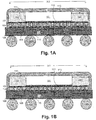
- Fig. 1A is a side cutaway view of an example semiconductor device in accordance with one or more aspects described herein.
- the semiconductor device of Fig. 1A may include a semiconductor chip or die 101 that may include one or more active and/or passive components, such as electrical and/or optical components.
- the semiconductor chip 101 may include components such as one or more resistors, transistors, capacitors, diodes, and/or memory cells, with one or more conductive lines interconnecting the same.
- the semiconductor device of Fig. 1A (as well as the devices of Figs. 1B, 2A, 2B, 3, and 5-10 ) may be considered a flip-chip package, and accordingly the semiconductor chip 101 may be oriented in what is commonly referred to as a flip-chip configuration relative to the remainder of the semiconductor device.
- one or more electrically conductive contacts (e.g., pads) 111 on or otherwise at a first surface 112 of the semiconductor chip 101 face downward in Fig. 1A .
- the conductive pads 111 allow the semiconductor chip 101 to electrically communicate with other portions of the semiconductor device.
- the semiconductor chip 101 may be at least partially surrounded in one or more lateral directions by an extension layer 102.
- the extension layer 102 may be made of a plastic material, mold compound, or other non-conductive material, and may be directly adjacent to and/or in contact with one or more lateral sides of the semiconductor chip 101.
- the extension layer 102 may artificially extend the surface area of the semiconductor chip 101, and may be made of a material different than the material of the semiconductor chip 101. In doing so, the extension layer 102 may extend the area of the lower surface 112 of the semiconductor chip 101 by an area that may be flush (at the same level) and/or continuous with the lower surface 112 of the semiconductor chip 101. However, the lower surface of the extension layer 102 may be at a slightly different level than the lower surface 112 of the semiconductor chip 101, if desired.
- the pads 111 of the semiconductor chip 101 may be electrically coupled to one or more conductive electrical connections of a redistribution layer (RDL) 107.
- the RDL 107 may be disposed on the underside of at least a portion of the chip 101 and on the underside of at least a portion of the extension layer 102.
- the RDL 107 may be further electrically coupled to (for instance, in direct electrical contact with) a first-level interconnect, illustrated in this example as one or more electrical connectors that may be in the form of, e.g., copper cylinders 105, or in the example of Fig. 1B , solder bumps 115.
- the electrical connectors 105/115 may, in turn, be electrically coupled to (for instance, in direct electrical contact with) an interposer 114.
- the interposer 114 may redistribute and/or re-map connections from the electrical connectors 105/115 to a ball grid array (BGA) of solder balls 106 disposed on the underside of the interposer 114.
- BGA ball grid array
- the BGA may, in turn, be electrically coupled to (e.g., soldered to) a circuit board such as a PCB board.
- the example semiconductor devices described herein may be placed on a circuit board as part of a larger circuit and/or device.
- the interposer 114 may have one or more electrical contacts 108 (e.g., pads) at an upper surface of the interposer 114 that are electrically coupled (and in physical contact) with the electrical connectors 105/115.
- the interposer 114 may further have one or more electrical contacts 110 at an opposite lower surface of the interposer 114 that are electrically coupled (and in physical contact) with the solder balls 106 of the BGA.
- the contacts 108 and 110 may be distributed over a surface area that is larger than the surface area over which the pads 111 are distributed (e.g., larger than the surface area of the semiconductor chip 101).
- the contacts 108 and 110 may be disposed underneath the extension layer 102 but not underneath the semiconductor chip 101.
- the electrical contacts 108 and the electrical contacts 110 may be interconnected by a one or more interconnects 109 disposed fully or partially within the interposer 114.
- the interconnects 109 may carry electrical signals from one or more of the electrical contacts 108 to one or more of the electrical contacts 110, and/or vice-versa, as desired.
- the electrical contacts 110 may be arranged on the interposer 114 so as to have a pitch that is equal to or larger than the pitch of the electrical contacts 108.
- the respective quantities of the electrical contacts 108 and 110 may or may not be equal.
- the extension layer 102 may extend from the side(s) of the semiconductor chip 101 in one or more lateral directions by a non-zero distance E.
- the distance E may depend upon the area of the semiconductor chip 101, the pad pitch of the semiconductor chip 101, the quantity of the pads 111, a number of the electrical contacts 108, and/or a desired pitch of the electrical contacts 108. Since the total surface area provided by the extension layer 102 combined with the semiconductor chip 101 will be increased as compared with only the surface area of the semiconductor chip 101, this may allow for the pitch of the electrical contacts 108 to be larger than the pitch of the pads 111.
- the pitch of a two-dimensional array of pads or other elements may refer to the pitch in each of two orthogonal directions defined by the array (such as rows and columns).
- the pitch in the two directions may or may not be the same for a given array.
- the interposer 114 may be made of, or otherwise include, a printed circuit board (PCB), and may be formed as a dielectric substrate on and/or in which electrically conducting layers may be formed to provide the above-mentioned interconnects 109.
- the interposer 114 may be formed of a network of the conducting layers that are made of thin copper or other metal foil and that are embedded into and/or patterned onto dielectric materials such as polytetrafluoroethylene (TEFLON), resin bonded paper, cotton paper and epoxy, or glass and epoxy.
- TEFLON polytetrafluoroethylene
- the material(s) of the interposer 114 may be selected to have a coefficient of thermal expansion (CTE) close to that of the PCB onto which the ball grid array 106 is to be soldered. In doing so, this may reduce the possibility of the interposer 114 and the PCB board external to the semiconductor device pulling away from each other and potentially causing circuit disconnections or short-circuiting due to environmental temperature variations.
- the interposer 114 may be made of other materials, such as low temperature co-fired ceramic (LTCC), high temperature co-fired ceramic (HTCC), or flexible substrate material (e. g. polyimide foil, PET foil), if desired, however it believed that PCB may be a more cost-effective material, especially because this material is relatively inexpensive and is already being used in conventional flip-chip devices.
- LTCC low temperature co-fired ceramic
- HTCC high temperature co-fired ceramic
- flexible substrate material e. g. polyimide foil, PET foil
- At least a portion of the semiconductor device may also be covered and/or filled with an underfill material 103 to potentially provide protection from external forces and/or to potentially prevent temperature changes (and any differences in the various CTEs of the elements of the semiconductor device) from causing cracking or separation of the various elements of the semiconductor device.
- the underfill material 103 may be made of any non-conductive material, such as plastic.
- the underfill material 103 may be partially or fully disposed, for example, on an upper surface 113 of the semiconductor chip 101, an upper surface of the extension layer 102, the sides of the extension layer 102, and/or in the otherwise empty region between the RDL 107 and the interposer 114.
- the underfill material 103 may further be partially or fully disposed on the sides of the interposer 114, if desired. Any types of underfill materials may be used, such as capillary flow underfill, molded underfill, pre-applied (no-flow-) underfill, or wafer level underfill.
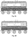
- the extension layer 102 does not cover the upper surface 113 of the semiconductor chip 101. This may be desirable, as it may prevent or reduce any bi-metal effects between the extension layer 102 and the surface 113 of the semiconductor chip 101 that might otherwise exist. However, if desired, the extension layer 102 may partially or completely cover the surface 113 of the semiconductor chip 101.
- Figs. 2A and 2B which correspond respectively to Figs. 1A and 1B , show examples of such a configuration.
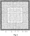
- the laterally extending nature of the extension layer 102 is also shown by way of example in the top plan view of Fig. 3 (viewed from point of view 3-3 as indicated in Figs. 1A and 1B ).
- Fig. 3 may also apply to the examples of Figs. 2A and 2B , except that the extension layer 102 would also be shown to cover the otherwise exposed surface of the semiconductor chip 101.
- the extension layer 102 extends symmetrically in all four lateral directions (up, down, left, and right in the view of Fig. 3 ).
- the extension layer 102 may alternatively extend symmetrically or asymmetrically in only one, two, or three of the directions.
- Fig. 3 may also apply to the examples of Figs. 3 .
- the extension layer 102 may extend in any one or more of the four directions by respective distances E1, E2, E3, and E4, which may each be zero or any non-zero distance as desired. While distances E1, E2, E3, and E4 may each be the same amount of distance, they may also be different from each other. For instance, distances E1 and E2 may be non-zero (and may be equal to each other) while distances E3 and E4 may be both zero.
- the electrical connectors 105/115 may extend laterally in one or more directions from the underside of the semiconductor chip 101.
- the electrical connectors 105/115 may be distributed across the combined lateral area defined by the semiconductor chip 101 and the extension layer 102. This means that, while the pads 111 of the semiconductor chip 101 may be distributed within the smaller lateral area of the semiconductor chip 101, the electrical connectors 105/115 may be provided a larger area in which to be distributed. Therefore, where the quantity of the pads 111 and the quantity of electrical connectors 105/115 are the same or are similar, the electrical connectors 105/115 may be able to be provided at a larger pitch than the pitch of the pads 111.
- the pitch of the pads 111 of the semiconductor chip 101 may be distributed at a first pitch
- the pitch of the electrical connectors 105/115 may be distributed at a second pitch that is larger than the first pitch
- the solder balls 106 of the BGA may be distributed at a third pitch that is larger than the second pitch.
- the semiconductor chip 101 may be made relatively small in area, with a relatively large number of pads 111, and the semiconductor device (e.g., of Figs.
- 1A, 1B , 2A, 2B , or 3 may re-map the pitch of pads 111 (the first pitch) to an intermediary pitch (the second pitch), and may further re-map the second pitch to the third pitch of the solder balls 106 so as to be appropriate for use as a BGA on a standard flip chip pad array of a customer PCB board (for example).
- the first, second, and third pitches may be any pitches desired.
- the first pitch (the pitch of the pads 111 of the semiconductor chip 101) may be in the range of 80 microns to 150 microns, in the range of 80 micron to 120 micron pitch, below 120 micron pitch, or below 100 micron pitch.
- the second pitch (the pitch of the electrical connectors 105/115) may be in the range of 100 micron pitch to 150 micron pitch, in the range of 100 micron pitch to 200 micron pitch, in the range of 120 micron pitch to 200 micron pitch, at least 150 micron pitch, or at any pitch greater than the first pitch and less than (or equal to) the third pitch.
- the third pitch (the pitch of the solder balls 106 of the BGA) may be at any pitch greater than or equal to the second pitch, such as at least 400 micron pitch, in the range of 400 micron pitch to 500 micron pitch, or in the range of 300 micron pitch to 600 micron pitch.
- the RDL 107 may re-route the pads 111 at a pitch of in the range of 80 to 120 microns, to the electrical connectors 105/115 at a larger pitch in the range of 120 to 150 microns.
- the interposer 114 may re-route the pitch of the electrical connectors 105/115 to the solder balls 106 of the BGA at a pitch of between 400 and 500 microns.
- the semiconductor device may convert the pitch of the pads 111 of the semiconductor chip from a smaller pitch to a larger pitch that may be suitable for attachment to a PCB board of a consumer device such as a cellular telephone or computer.
- PCB boards contain arrays for accepting flip chip package BGAs. Such arrays often have pads with a pitch in the range of 400 microns to 500 microns.
- the RDL may re-map the pad pitch to an electrical connector 105/115 to a larger intermediary pitch, and the interposer 114 may re-map that electrical connector 105/115 pitch to a still larger pitch, say, in the range of 400 micron pitch to 500 micron pitch, in order to appropriately fit the solder balls 106 of the BGA on the pad array of the above-mentioned PCB board.
- solder bumps are not realizable with acceptable yield at pitches below about 120 microns due to the high risk of solder briding, and so instead copper cylinders are typically used.
- copper cylinders are generally more expensive and less reliable to manufacture than solder bumps.
- copper cylinders typically require more accurate picking and placing to properly align the cylinders than do devices utilizing solder bumps.
- the larger surface area of the RDL 107 may allow a pitch for the electrical connectors 105/115 to be provided that is large enough to allow solder bumps to be used (e.g., about 150 micron pitch).
- pitches may be of any values desired.
- a particular array or row of elements pads 111, electrical connectors 105/115, solder balls 106
- pads 111, electrical connectors 105/115, solder balls 106 may be represented herein as having a particular pitch, not all of those elements need be arranged in accordance with the pitch. For instance, a subset of the elements may be spaced further apart (at a greater pitch) than others in the array or row, or may be otherwise spaced unevenly.
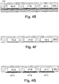
- Figs. 4A-4N are side cutaway views showing examples of a set of semiconductor devices during various steps of a manufacturing process.
- the set of semiconductor devices may be at least partially manufactured on a common carrier, and may be later separated from one another for further manufacturing.
- the various steps described in connection with Figs. 4A-4N may be used for manufacturing, for instance, the semiconductor devices of Figs. 1-3 and 5-10 . However, these semiconductor devices may be manufactured by alternative processes as desired.
- a carrier 401 may be provided, onto which the semiconductor device may be at least partially built.
- the carrier 401 may be made of any material, such as metal, silicon, or a polymer.
- an adhesive layer 402 may be applied to a top surface of the carrier 401.
- the adhesive layer 402 may be, for example, a foil with adhesive properties on both sides of the foil.
- the adhesive layer 402 may be provided such that the adhesive layer 402 is later releasable (i.e., not permanently adhesive), such as by the addition of energy in any form.
- each of the semiconductor chips 101 may be picked and placed so as to be attached to the adhesive layer 402.
- each of the semiconductor chips 101 are labeled with reference numbers 101-A, 101-B, 101-C, etc., in order to distinguish between each of the semiconductor devices being simultaneously manufactured on the same carrier 401. These will also be referred to herein collectively as the semiconductor chips 101.
- the various semiconductor chips 101 may all be the same type, size, and configuration of semiconductor chip, or they may be of different types, sizes, and/or configurations.
- the semiconductor chips 101 may be placed onto the adhesive layer 402 such that their pads 111 are facing, and, possibly in contact with, the adhesive layer 402. In other words, the semiconductor chips 101 may be placed in a flip-chip configuration down onto the adhesive layer 402 and the carrier 401.
- the carrier 401 and the adhesive layer 401 may be formed in the shape of, e.g., a circle with a notch 403, such as in the shape and size of a standard silicon wafer.
- the notch 403 may be used to align the carrier 401 with respect to various items of manufacturing equipment during any of the example manufacturing steps described herein. Any other formats of the carrier 401, such as rectangular, square, or another shape may alternatively be used. While notch 403 may be used as a rotation indicator, any other type of rotation indicator may be used, such as holes, marks, ID chips, placed marks, etc.
- an overmolding layer 404 may be formed over the semiconductor chips 101 and onto the exposed surface of the adhesive layer 402, which will be used to form the extension layers 102.
- the overmolding layer 404 may be, for instance, a non-conductive standard plastic mold compound typically used in semiconductor device manufacturing.
- the mold compound may be in the form of, for example, a paste-like substance that may be pressed downward under pressure to fill in the gaps between the semiconductor chips 101.
- Such overmolding is commonly used in the making of reconstituted wafers.
- the mold compound may be dispensed, for example, as a liquid in the center of a mold tool and may compressed using compression molding. This compression may cause the mold compound to flow towards the edges of the wafer and/or mold tool.
- the overmolding layer 404 may remain on the semiconductor chip 101, such as shown in Fig. 4E .
- the overmolding layer 404 may be eliminated (e.,g., by grinding) to remove or reduce potential bi-metal effects at the interfaces between the overmolding layer 404 and the semiconductor chips 101.
- the overmolding layer 404 may also not be removed from the semiconductor chips 101, and may remain to at least partially cover the semiconductor chips 101 in the final products if desired.
- the adhesive layer 402 and the carrier 401 may be removed from the overmolding 404 and the semiconductor chips 101.
- the pads 111 of each of the semiconductor chips 101 may be exposed (albeit the pads 111 may be covered by a thin layer of aluminum oxide or titanium nitride, for example).
- the resulting combination of the overmolding 404 and the semiconductor chips 101 may be considered a reconstituted wafer.
- the reconstituted wafer may have a shape such as shown in Fig. 4D , or another shape.
- a dielectric layer may be applied to the bottom of the reconstituted wafer, including the pads 111.
- the dielectric layer may be made of a material such as polyimide, PBO, BCB, Epoxy, or laminated film (e.g., ABF).
- the dielectric layer, if applied, may be structured so as to expose the pads 111, such as by photolithography or via a laser.
- the RDL 107 may be formed on the exposed semiconductor chips 101 and the exposed overmolding 404 (where the structured dielectric layer, if any, may be disposed between the RDL 107 and the semiconductor chips 101 and between the RDL 107 and the overmolding 404.
- the dielectric layer may be disposed between the reconstituted wafer and the RDL 107 and/ or a solder stop layer on top of the RDL 107 defining the landing area for the plurality of electrical connectors.
- each of the RDLs 107 are labeled with reference numbers 107-A, 107-B, 107-C, etc., in order to distinguish between each of the semiconductor devices being simultaneously manufactured on the same carrier 401. These will also be referred to herein collectively as the RDLs 107.
- the RDLs 107 may be formed and aligned in such a manner that the exposed electrical pads of the RDLs 107 are electrically coupled to the appropriate pads 111 of the respective semiconductor chips 101.
- the RDLs 107 may be formed by, for example, the use of standard sputtering, plating resist, electroplating, stripping, etching, electro-less processes, dispensing, and/or printing that may be commonly used to form redistribution layers. However, in the present example, the RDLs 107 may each extend beyond the lateral boundaries of the respective semiconductor chips, extending onto the underside of the overmolding 404 as shown in Fig. 4G . Moreover, electrically conductive pads on the underside of the RDLs 107 may be formed such that the electrically conductive pads (which are to be later coupled to the electrical connectors 105/115) are disposed both underneath the respective semiconductor chips 101 and underneath the overmolding 403 surrounding each of the semiconductor chips 101.
- the electrical connectors 105 or 115 may be applied to the RDLs 107.
- each of the electrical connectors are labeled with reference numbers 105-A, 105-B, 105-C, etc., in order to distinguish between each of the semiconductor devices being simultaneously manufactured on the same carrier 401. These will also be referred to herein collectively as the electrical connectors 105 (or 115, depending upon whether copper cylinders or solder bumps are used as the electrical connectors).
- the electrical connectors are copper cylinders 105 (such as in Fig.
- the copper cylinders 105 may be applied by, e.g., electroplating such as by re-using the seed layer previously used for creating the RDLs 107 at desired locations on the RDLs 107. Solder, tin, any other solderable material or alloy may then be applied to the exposed tip of each copper cylinder 105. Methods for creating such material-tipped copper cylinders are well-known in the art.
- the electrical connectors 115 are solder bumps 115
- the solder bumps 115 may be applied to the desired locations of the RDLs 107 such as in a conventional way (e.g., by plating or printing).
- a solder stop layer may be provided between the RDLs 107 and the solder bumps 115. While Figs. 4H-4N show manufacturing steps in which copper cylinders 105 are used, solder bumps 115 or other types of electrical connectors may alternatively be used for these same manufacturing steps.
- the various semiconductor devices 101 may then be separated from one another into s plurality of parts, such as by dicing the reconstituted wafer.
- the separations may be made at locations between the RDLs 107, such as shown by way of the vertical broken lines in Fig. 4H .
- the locations of separation may be made between the respective RDLs 107, such that each part retains intact at least one of the semiconductor chips 101 and their respective RDL 107 and electrical connectors 105/115.
- Fig. 4I An example of a resulting separated semiconductor device is shown in Fig. 4I .
- the overmolding 404 covering the semiconductor chip 101 may be fully or partially removed (e.g., thinned) such as by grinding. This may be desirable as it may eliminate any bi-metal warping effect caused by the excess overmolding 404 that might otherwise exist.
- Figs. 4I-4K show an example where the overmolding 404 is removed in this manner.
- Figs. 4L-4N correspond to Figs. 4I-4K , except that the overmolding 404 over the semiconductor chip 101 has not been eliminated.
- Fig. 4I shows a portion of the example semiconductor device that was previously described and illustrated with respect to Fig. 1A .
- the previously-described interposer 114 may be applied to the exposed copper cylinders 105 (or solder bumps 115), such that the copper cylinders 105 or solder bumps 115 are electrically connected to desired locations of the interposer 114.
- the previously-described underfill material 103 may be applied to the semiconductor device so as to fill desired regions of the semiconductor device.
- the underfill material 103 may improve the board level temperature cycling performance by, e. g., transforming any CTE differential shear forces between the semiconductor chip 101 and the interposer 114 into bending forces.
- the solder balls 106 of the BGA may be applied to desired locations on the underside of the interposer 114.
- the resulting semiconductor device may then be applied to a desired location of a circuit board 403, such as a PCB circuit board. This may be accomplished by, for instance, locating the BGA solder balls 106 on the desired location of the circuit board 403 and heating the solder balls 106 in order to sufficiently melt the solder balls 106 onto the appropriate electrical pads of the circuit board 403. After the solder balls 106 have cooled (and possibly after any other circuit board elements have been applied as desired), the semiconductor device may be tested in situ on the circuit board 403.
- the interposer 114 may include one or more passive and/or active circuit components (such as capacitors, resistors, transistors, diodes, and/or memory cells).
- the components included in the interposer 114 may be embodied as individual components and/or as collections of smaller components packaged together.
- the interposer 114 is adjacent to the RDL 107, the one or more circuit components may be embedded into the interposer 114 such that electrical contacts of those embedded circuit components may directly face electrical connectors 105/115 to connect to the RDL 107.
- semiconductor devices with an interposer 114 having one or more circuit components will now be discussed.
- Fig. 5 is a side cutaway view of an example of such a semiconductor device that includes an interposer-embedded circuit component, using copper cylinders 105 to connect between the RDL 107 and the interposer 114.
- Fig. 6 is a similar side cutaway view of an example a semiconductor device that includes the interposer-embedded circuit component, but instead uses solder bumps 115 to connect between the RDL 107 and the interposer 114.
- the present examples of Fig. 5 and 6 also include a circuit component 501 disposed partially or fully within the interposer 114.
- the circuit component 501 may include one or more elements such as transistors, capacitors, resistors, transistors, memory elements, and/or the like, which may be embodied in a package such as in the form of a semiconductor chip.
- the circuit component 501 may be positioned in the interposer 114 such that one or more electrical contacts 502 of the circuit component 501 may face and be directly electrically coupled with one or more of the electrical connectors 105/115.
- the electrical contacts 502 of the circuit component 501 may be laterally aligned and/or in direct physical contact with the respective electrical connectors 105/115. This alignment and direct face-to-face contact between the circuit component 501 and the electrical connectors 105/115 may allow for increased performance of the semiconductor device, e.g., by providing a potentially faster and/or more reliable signal link between the semiconductor chip 101 and the circuit component 501.
- the circuit component 501 may be deeply embedded in the interposer 114 such that the circuit component 501 communicates with the semiconductor chip 101 via separate conductive lines, such as via interconnects 109, between the circuit component 501 and the electrical connectors 105/115. Additionally or alternatively, the circuit component 501 may be oriented such that some or all of the electrical contacts 502 of the circuit component 501 face away from the electrical connectors 105/115. For instance, if desired, the circuit component 501 may be embedded in a face-down orientation, where the electrical contacts 502 face toward the solder balls 106 of the BGA.
- such a face-down orientation may utilize additional interconnect lines and/or wires and so may not result in the relative performance improvements that may be potentially realized in the face-up orientation of the circuit component 501 (where the electrical contacts 502 face toward the electrical connectors 105/115), such as shown in Fig. 5 .
- FIG. 7 shows a semiconductor device having two semiconductor chips 101-A and 101B and two interposer-embedded circuit components 501-A and 501-B.
- the example of Fig. 8 is similar to that of Fig. 7 , except that the solder bumps 115 are used rather than the copper cylinders 105.
- the circuit components 501-A and 501-B may be partially or fully embedded in the interposer 114, and may be aligned so as to directly align and/or contact with desired ones of the electrical connectors 105/115.
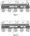
- Figs. 9 and 10 illustrate yet further example embodiments.
- the example of Fig. 9 is similar to that of Fig. 7 , except that the underfill material 103 does not cover the upper side of the semiconductor device.
- the surface 113 of the semiconductor chip(s) 101 facing away from the electrical connectors 105/115 may be exposed and/or partially or fully covered by another material, depending upon whether the above-mentioned grinding has been performed.
- the example of Fig. 10 is similar to that of Fig. 9 , except that the solder bumps 115 are used rather than the copper cylinders 105.
- the embodiments of Figs. 9 and 10 show multiple semiconductor chips 101 and multiple circuit components 501 embedded in the interposer 114, these embodiments may have any number of one or more semiconductor chips 101 and any number of zero or more circuit components 501.
- the interposer 114 may be divided into multiple separate interposers laid out side by side, such as one interposer per semiconductor chip 101 and/or one interposer per circuit component 501.
- the interposer 114 may be divided into multiple separate interposers laid out side by side, such as one interposer per semiconductor chip 101 and/or one interposer per circuit component 501.
- embodiments having particular numbers of semiconductor chips 101 and circuit components 501 are shown in the drawings, other embodiments may have any combination of quantities of semiconductor chips 101 and circuit components 501 (or lack thereof), as desired.
- an embodiment may have only a single semiconductor chip 101 and two or more circuit components 501 embedded in one or more interposers 114.
- an embodiment may have two or more semiconductor chips 101 and only a single circuit component 501 embedded in the interposer 114 (or embedded in one of multiple interposers 114).
- the extension layer 102 may partially or completely cover the surface 113 of any of the one or more semiconductor chips 101 in any of the examples of Figs. 5-10 , similar to extension layer 102 configuration shown in Figs. 2A and 2B .
- Figs. 11A-11D are side cutaway views showing examples of the interposer 114 during various steps of a process for manufacturing the interposer 114 while embedding one or more circuit components (such as the circuit component 501) in a face-up configuration in the interposer (such as the interposer 114).
- the interposer 114 is a PCB board.
- the interposer 114 may be made of alternative materials and configuration, and so the steps for embedding the circuit component 501 and manufacturing the interposer 114 may differ accordingly.
- the circuit component 501 may be placed on a carrier 1101.
- the carrier 1101 may be made of an electrically conductive material, such as copper or another metal.
- the circuit component 501 may be attached to the carrier 1101 using an adhesive 1102.
- the circuit component 501 may be oriented such that the electrical contacts 502 face away from the carrier 1101. While only a single circuit component 501 is shown in this example, it will be understood that multiple circuit components 501 may be placed onto the carrier 1101 during this step or during another manufacturing step.
- a laminate material 1103, such as epoxy (into which paper or woven glass, for example, may be embedded), may be applied to the combined carrier and circuit component 501.
- the laminate material 1103 may thus cover the exposed surfaces of the circuit component 501 and the exposed surface of the carrier 1103 side that is facing the circuit component 501.
- one or more vias 1104 in the molding material 1103 may be formed, such as by laser drilling.
- the vias 1104 may be formed at strategic locations so as to align with, for example, one or more of the electrical contacts 502 and/or one or more regions in which a through via is desired to extend completely through the molding material 1103 down to the carrier 1101.
- the one or more vias 1104 may be filled with an electrically conductive material 1105, such as copper or another metal.
- the upper surface of the molding material 1103 may also be selectively coated in a pattern of the conductive material 1105, to form the electrical contacts 108 of the interposer 114.
- the carrier 1101 may also be patterned so as to form multiple different electrical regions that may form the electrical contacts 110 of the interposer 114.
- the vias 1104 that extend completely through the molding material 1103 may be filled with the conductive material 1105 such that the conductive material 1105 electrically couples one or more portions of the carrier 1101 with one or more portions of the conductive material 1105. These vias may form at least a portion of the previously-mentioned interconnects 109 of the interposer 114. Other conventional manufacturing steps may be implemented to create more complex portions of the interconnects 109, as desired.
- the resulting interposer 114 may be used in a semiconductor device as described herein, such as in any of the semiconductor devices illustrated in Figs. 1-3 and 5-10 .
- a fan-out structure may be used to translate the pitch of a semiconductor chip to a lower intermediary pitch within a flip-chip package.
- This may eliminate the need for the expensive silicon or glass interposer that is conventionally used in 2.5D flip-chip packages. Rather, one may simply create an extension layer to provide a lateral fan-out region, use an RDL on the combined semiconductor chip and extension layer to reduce the semiconductor chip pad pitch to a pitch that is compatible with a PCB interposer, and then couple a PCB or similar interposer to the RDL to further reduce the pitch as needed to a larger circuit board pitch and to closely match the CTE of the flip chip package to the CTE of the circuit board. Moreover, this may all be done in an inexpensive way using conventional flip-chip materials and conventional manufacturing techniques.
- a semiconductor device including: a first semiconductor chip having at least one electrically conductive contact at a first side of the first semiconductor chip; an extension layer extending laterally from one or more sides of the first semiconductor chip; a redistribution layer disposed on a surface of the extension layer and the first side of the first semiconductor chip, the redistribution layer being electrically coupled to the at least one electrically conductive contact of the first semiconductor chip; an interposer having at least one electrically conductive contact at a first surface of the interposer and at least one electrically conductive contact at a second surface of the interposer opposite to the first surface of the interposer, the at least one electrically conductive contact at the first surface of the interposer being electrically coupled to the redistribution layer; and a molding material at least partially enclosing the first semiconductor chip and the redistribution layer, and in contact (e.g. direct contact, e.g. physical contact) with the interposer.
- contact e.g. direct contact, e.g. physical contact
- the interposer may include or may be a Printed Circuit Board (PCB) interposer.
- PCB Printed Circuit Board
- the at least one electrically conductive contact of the first semiconductor chip may be part of a first plurality of electrically conductive contacts at the first side of the first semiconductor chip, and the at least one electrically conductive contact at the first surface of the interposer may be part of a second plurality of electrically conductive contacts at the first surface of the interposer, wherein a first pitch of the first plurality of electrically conductive contacts is smaller than a second pitch of the second plurality of electrically conductive contacts.
- the first pitch may be below a 100 micron pitch and the second pitch may be at least a 150 micron pitch.
- the first pitch may be below a 100 micron pitch, wherein the semiconductor device further includes a plurality of solder bumps at the second pitch each electrically connecting one of the second plurality of electrically conductive contacts with the redistribution layer.
- the second pitch may be smaller than a third pitch of the third plurality of electrically conductive contacts.
- the semiconductor device may further include a circuit component embedded in the interposer, the circuit component having at least one electrically conductive contact facing the first semiconductor chip.
- the circuit component may include or be a second semiconductor chip.
- the extension layer may extend from at least four sides of the first semiconductor chip.
- the extension layer may be made of a material different than the first semiconductor chip.
- the at least one electrically conductive contact at the first surface of the interposer may be part of a plurality of electrically conductive contacts at the first surface of the interposer, at least one of the plurality of conductive contacts may be disposed under the extension layer, and at least another of the plurality of conductive contacts may be disposed under the first semiconductor chip.
- a semiconductor device including: a first semiconductor chip having at least one electrically conductive contact at a first side of the first semiconductor chip; an extension layer extending laterally from one or more sides of the first semiconductor chip; a redistribution layer disposed on a surface of the extension layer and the first side of the first semiconductor chip, the redistribution layer electrically coupling the at least one electrically conductive contact of the first semiconductor chip to at least one electrical connector; and an interposer electrically coupled to the at least one electrical connector and having a plurality of electrically conductive contacts at a surface of the interposer facing away from the redistribution layer; and a ball grid array disposed on the plurality of electrically conductive contacts of the interposer.
- the semiconductor device may further include a molding material at least partially enclosing the first semiconductor chip and the redistribution layer, and in contact (e.g. direct contact, e.g. physical contact) with the interposer.
- a molding material at least partially enclosing the first semiconductor chip and the redistribution layer, and in contact (e.g. direct contact, e.g. physical contact) with the interposer.
- the at least one electrical connector may include or may be a plurality of solder bumps disposed between the redistribution layer and the interposer.
- a pitch of the plurality of solder bumps may be below a 100 micron pitch.
- the at least one electrical connector may include or may be a plurality of copper pillars disposed between the redistribution layer and the interposer.
- the at least one electrically conductive contact of the first semiconductor chip may be part of a first plurality of electrically conductive contacts at the first side of the first semiconductor chip, and the at least one electrical connector may be part of a plurality of electrical connectors electrically coupled to the interposer, wherein a first pitch of the first plurality of electrically conductive contacts is smaller than a second pitch of the plurality of electrical connectors.
- the first pitch may be below a 100 micron pitch and the second pitch may be at least a 150 micron pitch.
- the second pitch may be smaller than a third pitch of the ball grid array.
- the semiconductor device may further include a circuit component embedded in the interposer, the circuit component having at least one electrically conductive contact facing the first semiconductor chip.
- the circuit component may include or be a second semiconductor chip.
- the at least one electrical connector may be part of a plurality of electrical connectors electrically coupled to the interposer, at least one of the plurality of electrical connectors may be disposed under the extension layer, and at least another of the plurality of electrical connectors may be disposed under the first semiconductor chip.
- the semiconductor device may further include a second semiconductor chip having at least one electrically conductive contact at a first surface of the second semiconductor chip that is facing in a same direction as the first surface of the first semiconductor chip, wherein the extension layer further extends laterally from one or more sides of the second semiconductor chip, and wherein the redistribution layer is further disposed on the first surface of the second semiconductor chip, and wherein the at least one electrical connector is part of a plurality of electrical connectors electrically coupled to the interposer, and wherein the redistribution layer electrically couples the at least one electrically conductive contact of the second semiconductor chip to at least another of the plurality of electrical connectors.
- a method for manufacturing a semiconductor device including: forming a redistribution layer on a surface of a layer that includes a first semiconductor chip and an extension layer, wherein the redistribution layer extends beyond a boundary of the first semiconductor chip; forming a plurality of electrical connectors on the redistribution layer, wherein a first electrical connector of the plurality of electrical connectors is disposed within the boundary of the first semiconductor chip and a second electrical connector of the plurality of electrical connectors is disposed outside of the boundary of the first semiconductor chip; connecting an interposer to the plurality of electrical connectors; and forming a ball grid array on a surface of the interposer that is opposite the plurality of electrical connectors.
- the method may further include enclosing at least a portion of the first semiconductor chip and the redistribution layer in a molding material, wherein the molding material further contacts the interposer, and wherein the ball grid array is exposed by the molding material.
- the interposer may include or may be a Printed Circuit Board (PCB) interposer.
- PCB Printed Circuit Board
- a first pitch of electrically conductive contacts of the first semiconductor chip may be smaller than a second pitch of the electrical connectors, wherein the second pitch is smaller than a third pitch of the ball grid array.
- the plurality of electrical connectors may include or may be a plurality of copper cylinders.
- the plurality of electrical connectors may include or may be a plurality of solder bumps.
- a first pitch of electrically conductive contacts of the first semiconductor chip may be below a 100 micron pitch.
- the method may further include embedding a second semiconductor chip in the interposer.
- a method for manufacturing a plurality of semiconductor devices including: forming a redistribution layer on a surface of a reconstituted wafer, the reconstituted wafer including at least a plurality of semiconductor chips, wherein for each of the plurality of semiconductor chips, the redistribution layer extends beyond a boundary of the semiconductor chip; forming a plurality of electrical connectors on the redistribution layer, wherein for each of the plurality of semiconductor chips, a first electrical connector of the plurality of electrical connectors is disposed within the boundary of the semiconductor chip and a second electrical connector of the plurality of electrical connectors is disposed outside of the boundary of the semiconductor chip; separating the reconstituted wafer into a plurality of parts, each of the parts including at least one of the plurality of semiconductor chips and the respective electrical connectors for the at least one of the plurality of semiconductor chips; for each of the parts, connecting an interposer to the plurality of electrical connectors; and for each of the parts, forming a ball grid array on a
- the method may further include, for each of the parts, at least partially enclosing the part in a molding material wherein the ball grid array is exposed.
- the interposer may include or may be a Printed Circuit Board (PCB) interposer.
- PCB Printed Circuit Board
- the plurality of electrical connectors may include or may be a plurality of solder bumps.
- a pitch of electrically conductive contacts of the respective semiconductor chip may be below a 100 micron pitch.
- high quality passive devices e.g. inductors, capacitors or resistors
- SoC system-on-chip
- RF radio frequency
- IPD integrated passive devices
- frequency dependent devices like inductors or combinations of inductors (e.g. transformers) in mobile systems.
- inductors e.g. transformers
- present disclosure may also apply for other passive devices, like resistors and capacitors, and may not be limited to mobile applications.
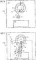
- One solution to bring passive devices such as inductors closer to the active circuitry on the chip may be to remove the rather area-consuming inductors from the SoC Si-chip (very expensive chip area) and place them into the redistribution layer (RDL) layers of a typical embedded wafer level ball grid array (eWLB) package, especially in the fan-out region over the mold (dielectric) material in order to reduce parasitic losses (e.g. Eddy currents) in the silicon substrate.
- RDL redistribution layer
- eWLB embedded wafer level ball grid array
- Another approach may be to place a second chip or at least a second piece of conductor into the fan-out region in the neighborhood of a primary chip in order to provide a conductive underpath from the center of the spiral coil to the eWLB RDL interconnect outside of the spiral coil.
- this approach may also increase manufacturing costs.
- this disclosure proposes a new package option, '2.5D eWLB/FC interposer', which may combine a typical eWLB package (having e.g. a simple single layer (1L) RDL in eWLB (which may e.g. save costs), however in principle two layer (2L), three layer (3L), or even more layer, RDLs may be possible as well) with a rather simple laminate (e.g. a 2L laminate (which may e.g. save costs), however also 4L, 6L, or even more metallization levels in laminate are possible as well), as described herein above and also shown in Fig. 12 .
- a typical eWLB package having e.g. a simple single layer (1L) RDL in eWLB (which may e.g. save costs), however in principle two layer (2L), three layer (3L), or even more layer, RDLs may be possible as well) with a rather simple laminate (e.g. a 2L laminate (which may e.g.
- Coupled or “connection” as used herein may be understood to include a direct “coupling” or direct “connection” as well as an indirect “coupling” or indirect “connection”, respectively.
- formed over are intended to include arrangements where a first element or layer may be formed, deposited, disposed, located or arranged directly on a second element or layer with no further elements or layers in-between, as well as arrangements where a first element or layer may be formed, deposited, disposed, located or arranged above a second element or layer with one or more additional elements or layers between the first element or layer and the second element or layer.
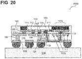
- Fig. 12 is a side cutaway view of a semiconductor device 1200 in accordance with one or more aspects described herein.
- the semiconductor device is to some degree similar to one or more of the semiconductor devices described herein above, for example the semiconductor device shown in Fig. 1B , and the same reference numerals may denote the same or similar elements as herein above.
- the semiconductor device 1200 may include a semiconductor chip or die 101 that may include one or more active and/or passive components, such as electrical and/or optical components.
- the semiconductor chip 101 may include components such as one or more resistors, transistors, capacitors, diodes, and/or memory cells, with one or more conductive lines interconnecting the same.
- the semiconductor device 1200 may be considered a flip-chip package, and accordingly the semiconductor chip 101 may be oriented in what may be commonly referred to as a flip-chip configuration relative to the remainder of the semiconductor device 1200.
- one or more electrically conductive contacts (e.g., pads) 111 on or otherwise at a first surface 112 of the semiconductor chip 101 face downward in Fig. 12 .
- the conductive pads 111 may allow the semiconductor chip 101 to electrically communicate with other portions of the semiconductor device 1200.
- the semiconductor chip 101 may be at least partially surrounded in one or more lateral directions by an extension layer 102.
- the extension layer 102 may include or may be composed of a plastic material, mold compound, or other non-conductive material, and may be directly adjacent to and/or in contact with one or more lateral sides of the semiconductor chip 101.
- the extension layer 102 may artificially extend the surface area of the semiconductor chip 101, and may be composed of a material different than the material of the semiconductor chip 101. In doing so, the extension layer 102 may extend the area of the lower surface 112 of the semiconductor chip 101 by an area that may be flush (at the same level) and/or continuous with the lower surface 112 of the semiconductor chip 101. However, the lower surface of the extension layer 102 may be at a slightly different level than the lower surface 112 of the semiconductor chip 101, if desired.
- the pads 111 of the semiconductor chip 101 may be electrically coupled to one or more conductive electrical connections of a redistribution layer (RDL) 107.
- the RDL 107 may be disposed on the underside of at least a portion of the chip 101 and on the underside of at least a portion of the extension layer 102.
- the RDL 107 may include or be composed of at least one electrically conductive material, e.g. a metal or metal alloy, such as copper or a copper alloy (other metals or metal alloys may be possible as well), which, may e.g. be disposed over an electrically conductive adhesion layer including or consisting of e.g. Ta, TaN, Ti, TiN, and/or TiW, or the like.
- a dielectric 120 may be disposed between portions of the RDL 107 and between the pads 111 to electrically insulate the pads 111 and the RDL 107.
- the RDL 107 may be further electrically coupled to (for instance, in direct electrical contact with) a first-level interconnect, illustrated in this example as one or more electrical connectors that may be in the form of, e.g., solder bumps 115 (e.g. flip-chip bumps, ⁇ -bumps), as shown here, or metal cylinders or pillars (e.g. copper cylinders or pillars) (not shown here, see e.g. copper cylinders 105 shown in Fig. 1A ).
- solder bumps 115 e.g. flip-chip bumps, ⁇ -bumps
- metal cylinders or pillars e.g. copper cylinders or pillars
- the electrical connectors may, in turn, be electrically coupled to (for instance, in direct electrical contact with) an interposer 114.
- the interposer 114 may redistribute and/or re-map connections from the electrical connectors, e.g. solder bumps 115, to a ball grid array (BGA) of solder balls 106 disposed on the underside of the interposer 114.
- the BGA may, in turn, be electrically coupled to (e.g., soldered to) a circuit board 116 such as a PCB board.
- a circuit board 116 such as a PCB board.
- the interposer 114 may have one or more electrical contacts 108 (e.g., pads) at an upper surface of the interposer 114 that may be electrically coupled (and in physical contact) with the electrical connectors 105 ( Fig. 1A ) or with the electrical connectors 115 ( Fig. 1B and Fig. 12 ).
- the interposer 114 may further have one or more electrical contacts 110 at an opposite lower surface of the interposer 114 that may be electrically coupled (and in physical contact) with the solder balls 106 of the BGA.
- the contacts 108 and 110 may be distributed over a surface area that is larger than the surface area over which the pads 111 are distributed (e.g., larger than the surface area of the semiconductor chip 101).
- at least some of the contacts 108 and 110 may be disposed underneath the extension layer 102 but not underneath the semiconductor chip 101.
- the interposer 114 may further have one or more interconnects 109 that may interconnect the electrical contacts 108 and the electrical contacts 110.
- the interconnects 109 may carry electrical signals from one or more of the electrical contacts 108 to one or more of the electrical contacts 110, and/or vice-versa, as desired.
- the electrical contacts 110 may be arranged on the interposer 114 so as to have a pitch that is equal to or larger than the pitch of the electrical contacts 108.
- the respective quantities of the electrical contacts 108 and 110 may or may not be equal.
- the extension layer 102 may extend from the side(s) of the semiconductor chip 101 in one or more lateral directions by a non-zero distance E.
- the distance E may depend upon the area of the semiconductor chip 101, the pad pitch of the semiconductor chip 101, the quantity of the pads 111, a number of the electrical contacts 108, and/or a desired pitch of the electrical contacts 108. Since the total surface area provided by the extension layer 102 combined with the semiconductor chip 101 will be increased as compared with only the surface area of the semiconductor chip 101, this may allow for the pitch of the electrical contacts 108 to be larger than the pitch of the pads 111.
- the pitch of a two-dimensional array of pads or other elements may refer to the pitch in each of two orthogonal directions defined by the array (such as rows and columns).
- the pitch in the two directions may or may not be the same for a given array.
- the interposer 114 may include or may be composed of a laminate material or laminate.
- the interposer 114 may be composed of, or otherwise include, a printed circuit board (PCB), and may be formed as a dielectric substrate on and/or in which electrically conducting layers may be formed to provide the above-mentioned interconnects 109.
- the interposer 114 may be formed of a network of the conducting layers that are made of thin copper or other metal foil and that are embedded into and/or patterned onto dielectric materials such as polytetrafluoroethylene, resin bonded paper, cotton paper and epoxy, or glass and epoxy.
- the material(s) of the interposer 114 may be selected to have a coefficient of thermal expansion (CTE) close to that of the PCB onto which the ball grid array 106 is to be soldered. In doing so, this may reduce the possibility of the interposer 114 and the PCB board external to the semiconductor device pulling away from each other and potentially causing circuit disconnections or short-circuiting due to environmental temperature variations.
- the interposer 114 may be made of other materials, such as low temperature co-fired ceramic (LTCC), high temperature co-fired ceramic (HTCC), or flexible substrate material (e. g. polyimide foil, PET foil), if desired, however it is believed that PCB may be a more cost-effective material, especially because this material is relatively inexpensive and is already being used in conventional flip-chip devices.
- LTCC low temperature co-fired ceramic
- HTCC high temperature co-fired ceramic
- flexible substrate material e. g. polyimide foil, PET foil
- the interposer 114 includes or is based on a semiconductor material such as silicon.
- the interposer 114 may be a silicon interposer having one or more through-silicon vias (TSVs).
- TSVs through-silicon vias
- the electrical contacts 108, 110 and interconnects 109 are electrically insulated from each other, for example by means of one or more insulating layers between the electrical contacts 108, 110 and interconnects 109 and the semiconductor material of the interposer 114.
- At least a portion of the semiconductor device may 1200 may also be covered and/or filled with an underfill material 103 to potentially provide protection from external forces and/or to potentially prevent temperature changes (and any differences in the various CTEs of the elements of the semiconductor device 1200) from causing cracking or separation of the various elements of the semiconductor device 1200.
- the underfill material 103 may be made of any non-conductive material, such as plastic.
- the underfill material 103 may be partially or fully disposed, for example, on an upper surface 113 of the semiconductor chip 101, an upper surface of the extension layer 102, the sides of the extension layer 102, and/or in the otherwise empty region between the RDL 107 and the interposer 114.
- the underfill material 103 may further be partially or fully disposed on the sides of the interposer 114, if desired. Any types of underfill materials may be used, such as capillary flow underfill, molded underfill, pre-applied (no-flow-) underfill, or wafer level underfill.
- the extension layer 102 does not cover the upper surface 113 of the semiconductor chip 101. This may be desirable, as it may prevent or reduce any bi-metal effects between the extension layer 102 and the surface 113 of the semiconductor chip 101 that might otherwise exist. However, if desired, the extension layer 102 may partially or completely cover the surface 113 of the semiconductor chip 101 (not shown here, see e.g. Figs. 2A and 2B ).
- the extension layer 102 is also shown by way of example in the top plan views of Fig. 3 (viewed from point of view 3-3 as indicated in Figs. 1A and 1B ) and Figs. 14 and 15 .
- the extension layer 102 may extend symmetrically in all four lateral directions (up, down, left, and right in the view of Fig. 3 ).
- the extension layer 102 may alternatively extend symmetrically or asymmetrically in only one, two, or three of the directions.
- the extension layer 102 may extend in any one or more of the four directions by respective distances E1, E2, E3, and E4, which may each be zero or any non-zero distance as desired.
- distances E1, E2, E3, and E4 may each be the same amount of distance, they may also be different from each other. For instance, distances E1 and E2 may be non-zero (and may be equal to each other) while distances E3 and E4 may be both zero.
- the electrical connectors 105/115 may extend laterally in one or more directions from the underside of the semiconductor chip 101.
- the electrical connectors 105/115 may be distributed across the combined lateral area defined by the semiconductor chip 101 and the extension layer 102. This means that, while the pads 111 of the semiconductor chip 101 may be distributed within the smaller lateral area of the semiconductor chip 101, the electrical connectors 105/115 may be provided a larger area in which to be distributed. Therefore, where the quantity of the pads 111 and the quantity of electrical connectors 105/115 are the same or are similar, the electrical connectors 105/115 may be able to be provided at a larger pitch than the pitch of the pads 111.
- the pitch of the pads 111 of the semiconductor chip 101 may be distributed at a first pitch
- the pitch of the electrical connectors 105/115 may be distributed at a second pitch that is larger than the first pitch
- the solder balls 106 of the BGA may be distributed at a third pitch that is larger than the second pitch.
- the semiconductor chip 101 may be made relatively small in area, with a relatively large number of pads 111, and the semiconductor device 1200 may re-map the pitch of pads 111 (the first pitch) to an intermediary pitch (the second pitch), and may further re-map the second pitch to the third pitch of the solder balls 106 so as to be appropriate for use as a BGA on a standard flip chip pad array of a customer PCB board (for example).
- the first, second, and third pitches may be any pitches desired.
- the first pitch (the pitch of the pads 111 of the semiconductor chip 101) may be in the range of 80 microns to 150 microns, in the range of 80 micron to 120 micron pitch, below 120 micron pitch, or below 100 micron pitch.
- the second pitch (the pitch of the electrical connectors 105/115) may be in the range of 100 micron pitch to 150 micron pitch, in the range of 100 micron pitch to 200 micron pitch, in the range of 120 micron pitch to 200 micron pitch, at least 150 micron pitch, or at any pitch greater than the first pitch and less than (or equal to) the third pitch.
- the third pitch (the pitch of the solder balls 106 of the BGA) may be at any pitch greater than or equal to the second pitch, such as at least 400 micron pitch, in the range of 400 micron pitch to 500 micron pitch, or in the range of 300 micron pitch to 600 micron pitch.
- the RDL 107 may re-route the pads 111 at a pitch of in the range of 80 to 120 microns, to the electrical connectors 105/115 at a larger pitch in the range of 120 to 150 microns.
- the interposer 114 may re-route the pitch of the electrical connectors 105/115 to the solder balls 106 of the BGA at a pitch of between 400 and 500 microns.
- the semiconductor device 1200 may convert the pitch of the pads 111 of the semiconductor chip 101 from a smaller pitch to a larger pitch that may be suitable for attachment to a PCB board of a consumer device such as a cellular telephone or computer.
- PCB boards contain arrays for accepting flip chip package BGAs. Such arrays often have pads with a pitch in the range of 400 microns to 500 microns.
- the RDL may re-map the pad pitch to an electrical connector 105/115 to a larger intermediary pitch, and the interposer 114 may re-map that electrical connector 105/115 pitch to a still larger pitch, say, in the range of 400 micron pitch to 500 micron pitch, in order to appropriately fit the solder balls 106 of the BGA on the pad array of the above-mentioned PCB board.
- solder bumps may not be realizable with acceptable yield at pitches below about 120 microns due to the high risk of solder briding, and so instead copper cylinders are typically used.
- copper cylinders may be generally more expensive and less reliable to manufacture than solder bumps.
- copper cylinders may typically require more accurate picking and placing to properly align the cylinders than do devices utilizing solder bumps.
- pitches may be of any values desired.
- a particular array or row of elements pads 111, electrical connectors 105/115, solder balls 106
- pads 111, electrical connectors 105/115, solder balls 106 may be represented herein as having a particular pitch, not all of those elements need be arranged in accordance with the pitch. For instance, a subset of the elements may be spaced further apart (at a greater pitch) than others in the array or row, or may be otherwise spaced unevenly.
- the semiconductor device 1200 may, for example, be manufactured using the various steps described in connection with Figs. 4A-4N . However, the semiconductor device 1200 may be manufactured by alternative processes as desired.
- the semiconductor device 1200 may be configured as 2.5D eWLB with a laminate as interposer and having a single level eWLB RDL and 2 level laminate interconnects. However, if needed, more eWLB RDL layers and laminate interconnect layers may be possible as well.
- this disclosure proposes an innovative use of the unique capabilities of the aforementioned '2.5D eWLB/FC interposer' package in combination with passive devices, especially spiral inductors realized in the single layer (1L) RDL over the fan-out area of the eWLB, by placing a typical FC bump pad (having e.g. typical FC bump pitches of about 200 ⁇ m to 150 ⁇ m) in the center of the spiral coil (in RDL) and providing a connection via solder bumps to a pad in the top interconnect level in the laminate underneath.
- This laminate interconnect may then be used as an underpath (overpath) under the spiral coil in the RDL.
- a second pad/solder bump connection may connect the underpath in the laminate with the eWLB RDL outside of the spiral area, and from there a connection to the circuitry on the semiconductor chip may be provided, see e.g. figures 13 and 14 .
- Fig. 13 is a side cutaway view of a semiconductor device 1300 having a redistribution layer 107 including a spiral coil 117, and an interposer 114 including an interconnect 118 coupled to a center contact 119 of the spiral coil 117.
- the semiconductor device 1300 is to some degree similar to the semiconductor device 1200 of Fig. 12 .
- the same reference signs may denote the same or similar elements as above and will not be described in detail again here for sake of brevity. Reference is made to the description above.
- the semiconductor device 1300 differs from the semiconductor device 1200 shown in Fig. 12 in that a circuit is integrated in the RDL 107 and the interposer 114.
- the circuit includes a first circuit portion and a second circuit portion, wherein the RDL 107 includes the first circuit portion and the interposer 114 includes the second circuit portion of the circuit.
- the circuit may be a passive circuit or passive circuit component such as an inductor, as shown.
- the first circuit portion includes or corresponds to a spiral coil 117
- the second circuit portion includes or corresponds to an interconnect 118 of an inductor.
- the spiral coil 117 may have one or a plurality of windings, which may be disposed substantially parallel to an interface between the interposer 114 and the RDL 107 ( FIG. 13 illustratively shows a cross-section through the windings of the spiral coil 117) and a center contact, e.g. a RDL bump pad 119 in the spiral center, that may be formed by material (e.g. metal or metal alloy) of the RDL 107.
- the interconnect 118 may be coupled (e.g. via an electrical connector, e.g a solder bump 115 as shown) to the center contact, e.g. bump pad 119 of the spiral coil 117, and may further be connected (e.g. via another electrical connector, e.g.
- the interconnect 118 may thus form an electrical underpath (i.e. inductor underpath in this example) in the interposer 114 (e.g. in the laminate) to connect an electrical contact of the first circuit portion (i.e. the center contact 119 of the spiral coil 117 in this example).
- Another contact of the first circuit portion may be connected directly to another electrically conductive contact, e.g. pad, 111 of the chip 101, i.e. without an underpath in the interposer 114.
- the spiral coil 117 may be disposed at least partially, e.g. entirely, between the interposer 114 and the extension layer 102, in other words, over the lower surface of the extension layer 102, and thus may be disposed e.g. over a fan-out region of the semiconductor chip 101. This may, for example, have the effect that generation of Eddy currents in the semiconductor chip 101 due to electromagnetic coupling between the spiral coil 117 and charge carriers of the semiconductor material (e.g. silicon) of the semiconductor chip 101 may be prevented or substantially reduced.
- the semiconductor material e.g. silicon
- spiral coil 117 (or, the first circuit portion) between the semiconductor chip 101 and the interposer 114, in other words, over the lower surface 112 of the semiconductor chip 101, for example in case that an extension layer 102 is not provided, but also in other cases.
- Fig. 13 shows a realization of an inductor underpath in the interposer material (e.g. laminate) to connect a coil center with an RDL (e.g. eWLB RDL) (and a chip) outside the spiral area.
- RDL e.g. eWLB RDL
- a solder bump may be placed in the center of the coil and may provide an electrical connection between the coil center (e.g. bump pad) and an interconnect of the interposer (e.g. laminate interconnect).
- a spiral coil may be formed within a single layer or level (1L) RDL and a center coil connection may be provided by an underpath provided by an interconnect in an interconnect level of the interposer.
- Fig. 14 is a plan view of a portion of a semiconductor device 1400 having a redistribution layer (RDL) 107 including a spiral coil 117, and an interposer 114 (not shown in Fig. 14 , see e.g. Fig. 13 ) including an interconnect 118 coupled to the spiral coil 117.
- the plan view of Fig. 14 illustratively shows various levels or layers, wherein the interconnect 118 is disposed in the bottommost level or layer in Fig.
- electrical connectors 115 (connecting the interconnect 118 with the RDL 107) are disposed in a higher level or layer than the interconnect 118, the RDL 107 (including the spiral coil 117) is disposed in a higher level or layer than the electrical connectors 115, and a chip 101 and an extension layer 102 are disposed in a higher level or layer than the RDL 107.
- the semiconductor device 1400 is to some degree similar to one or more of the semiconductor devices described herein above.
- the same reference signs may denote the same or similar elements as above and will not be described in detail again here for sake of brevity. Reference is made to the description above.
- the semiconductor device 1400 may include a semiconductor chip (e.g. silicon chip) 101, and an extension layer 102 laterally extending from at least one side of the chip 101 (in the example shown, the extension layer 102 extends from all four lateral sides of the chip 101, however the extension layer 102 may extend from only one, two, or three lateral sides of the chip 101).
- the chip 101 and the extension layer 102 may in each case be disposed over a portion of the redistribution layer 107 (see also Fig. 13 ).
- the extension layer 102 may be composed of material different from the chip 101.
- the extension layer 102 may, for example, be composed of a non-conductive material, for example one or more of the materials described herein above, e.g. a mold compound.
- the spiral coil 117 may be disposed between the extension layer 102 and the interposer 114.
- the extension layer 102 may serve as a fan-out region of the chip 101.
- the spiral coil 117 may be disposed over the fan-out region.
- the spiral coil 117 may have a center contact, e.g. RDL bump pad 119 that may be disposed in the spiral center and over the extension layer (fan-out region) 102.
- the interposer 114 may include an interconnect 118 that may connect the center contact 119 of the spiral coil 117 with the chip 101.
- another contact e.g. RDL bump pad 121 may be provided in the RDL 107 over the chip 101 and connected to the chip 101 (e.g. by means of a via connection 122, as shown), and the interconnect 118 may be connected to the contact (e.g. bump pad) 121 and thereby to the chip 101.
- Connection between the contacts 119, 121 (bump pads) and the interconnect 118 may, for example, be achieved by means of electrical connectors such as solder bumps 115 (as shown) or metal (e.g. Cu) cylinders or pillars.
- the interposer 114 may, for example, include a laminate, and the interconnect 118 may be disposed within the laminate. Thus, the interconnect 118 may form an electrically conductive underpath in the laminate below the RDL level.
- the semiconductor device 1400 may be configured as an eWLB package having a laminate interposer 114 and a single level eWLB RDL 107, wherein illustratively a spiral inductor 117 may be disposed in the RDL 107 over an eWLB fan-out region 102 and connected with a chip 101 via an underpath interconnect 118 disposed in the laminate of the laminate interposer 114.
- a width 130 of one or more RDL lines 107 forming the spiral coil 117 may, for example, be in the range from about 5 ⁇ m to 30 ⁇ m, e.g. from about 10 ⁇ m to about 25 ⁇ m, e.g. from about 15 ⁇ m to about 20 ⁇ m, although other values of the width 130 may be possible as well.
- the windings of spiral coil 117 are depicted as being composed of a rounded or curved spiral.
- the windings of the spiral coil 117 may be composed of angular shapes, e.g. rectangular, hexagonal, octagonal or other polygonal shapes of the spiral instead.
- a width 131 of the interconnect 118 may, for example, be in the range from about 15 ⁇ m to 50 ⁇ m, e.g. from about 20 ⁇ m to about 40 ⁇ m, e.g. from about 25 ⁇ m to about 30 ⁇ m, although other values of the width 131 may be possible as well.
- Fig. 15 is a plan view of a portion of a semiconductor device 1500 having a redistribution layer (RDL) 107 including a spiral coil 117, and an interposer 114 including interconnects 118, 118a coupled to the spiral coil 117.
- RDL redistribution layer
- the plan view of Fig. 15 illustratively shows various levels or layers, wherein the interconnects 118, 118a are disposed in the bottommost level or layer in Fig.
- electrical connectors 115 (connecting the interconnects 118, 118a with the RDL 107) are disposed in a higher level or layer than the interconnects 118, 118a, the RDL 107 (including the spiral coil 117) is disposed in a higher level or layer than the electrical connectors 115, and a chip 101 and an extension layer 102 are disposed in a higher level or layer than the RDL 107.
- the semiconductor device 1500 is to some degree similar to one or more of the semiconductor devices described herein above.
- the same reference signs may denote the same or similar elements as above and will not be described in detail again here for sake of brevity. Reference is made to the description above.
- the semiconductor device 1500 differs from the semiconductor device 1400 in that the inductor includes an additional interconnect 118a coupled to a peripheral contact, e.g. bump pad 123 of the spiral coil 117.
- the additional interconnect 118a may be connected to an additional contact, e.g. bump pad 124 provided over the chip 101, which in turn may be connected (e.g. by means of a via connection 122) to the chip 101.
- the semiconductor device 1500 may be configured as an eWLB package having a laminate interposer 114, wherein a spiral inductor coil 117 may be disposed in an eWLB RDL 107 and two underpath connections 118, 118a may be disposed in the laminate.
- a first underpath connection (interconnect 118) may connect a center contact, e.g. bump pad 119 of the spiral coil 117 with a first contact, e.g. bump pad 121 on the chip 101
- a second underpath connection additional interconnect 118a
- a width 132 of the additional interconnect 118a may, for example, be in the range from about 15 ⁇ m to 50 ⁇ m, e.g. from about 20 ⁇ m to about 40 ⁇ m, e.g. from about 25 ⁇ m to about 30 ⁇ m, although other values of the width 132 maybe possible as well.
- the width 132 of the additional interconnect 118a may be the same as the width 131 of the interconnect 118, or may be different from the width 131 of the interconnect 118.
- Fig. 16 is a plan view of a section of a semiconductor device 1600 having a redistribution layer (RDL) 107 including a spiral coil 117.
- RDL redistribution layer
- the plan view of Fig. 16 illustratively shows various levels or layers, wherein contacts of the interposer (e.g. bump pads on the laminate) are disposed in the bottommost level or layer in Fig.
- electrical connectors 115 (connecting the contacts of the interposer with the RDL 107) are disposed in a higher level or layer than the contacts of the interposer, the RDL 107 (including the spiral coil 117) is disposed in a higher level or layer than the electrical connectors 115, and a chip 101 and an extension layer 102 are disposed in a higher level or layer than the RDL 107.
- the semiconductor device 1600 is to some degree similar to one or more of the semiconductor devices described herein above.
- the same reference signs may denote the same or similar elements as above and will not be described in detail again here for sake of brevity. Reference is made to the description above.
- the center contact, e.g. the RDL bump pad 119 in the spiral center, of the coil 117 may be connected to a contact of the interposer 114 (e.g. to a bump pad on the laminate), and the peripheral contact, e.g. the RDL bump pad 123, of the coil 117 may be connected to another contact of the interposer (e.g. to another bump pad on the laminate).
- the center contact, e.g. the RDL bump pad 119 in the spiral center, of the coil 117 may be connected to a contact of the interposer 114 (e.g. to a bump pad on the laminate), and the peripheral contact, e.g. the RDL bump pad 123, of the coil 117 may be connected to another contact of the interposer (e.g. to another bump pad on the laminate).
- the peripheral contact e.g. the RDL bump pad 123
- the semiconductor device 1600 may be configured as an eWLB package having a spiral coil 117 disposed in the eWLB RDL 107, but having no direct connection of the coil 117 in the RDL 107 to the semiconductor chip 101 (e.g. silicon chip), i.e., to the chip in the same eWLB, but only a connection to a circuit board (e.g. PCB) 116 via the interposer 114.
- the coil 117 may be connected via a laminate interposer directly to a system board or alternatively to a neighboring chip on the same laminate in a side-by-side multi-chip package.
- Fig. 17 is a plan view of a portion of a semiconductor device 1700 having an interposer 114 including a spiral coil 117, and a redistribution layer (RDL) 107 including interconnects 128, 128a coupled to the spiral coil 117.
- RDL redistribution layer
- the plan view of Fig. 17 illustratively shows various levels or layers, wherein the interposer 114 (including the spiral coil 117) is disposed in the bottommost level or layer in Fig.
- electrical connectors 115 (connecting the spiral coil 117 with the interconnects 128, 128a of the RDL 107) are disposed in a higher level or layer than the interposer 114, the RDL 107 (including the interconnects 128, 128a) is disposed in a higher level or layer than the electrical connectors 115, and a chip 101 and an extension layer 102 are disposed in a higher level or layer than the RDL 107.
- the semiconductor device 1700 is to some degree similar to one or more of the semiconductor devices described herein above.
- the same reference signs may denote the same or similar elements as above and will not be described in detail again here for sake of brevity. Reference is made to the description above.
- a spiral coil 117 having one or more windings may be included in the interposer 114, e.g. composed of one or more interconnects 135 disposed e.g. within the laminate of a laminate interposer, while an interconnect 128 connecting a center contact, e.g. bump pad 119 of the coil 117 with the chip 101 and an additional interconnect 128a connecting a peripheral contact, e.g. bump pad 123 of the coil 117 with the chip 101 may be included in the redistribution layer 107.
- the interconnect 128 may serve as an electrically conductive overpath in this case to connect the center contact or port of the spiral coil 117.
- the windings of the spiral coil 117 are depicted as being composed of a rounded or curved spiral.
- the windings of the spiral coil 117 may be composed of angular shapes, e.g. rectangular, hexagonal, octagonal or other polygonal shapes of the spiral instead.
- the interposer 114 may have at least one interconnect level, e.g. a plurality of interconnect levels, and the spiral coil 117 may be disposed in one of the interconnect levels of the interposer 114.
- a width 133 of the interconnect 128 and/or a width 134 of the additional interconnect 128a in the RDL 107 may be similar or the same as described herein above for the width 130. Alternatively, the width 133 and/or width 134 may be different.
- a width 136 of the one or more interconnects 135 of the interposer 114 may be similar or the same as described herein above for the width 131. Alternatively, the width 136 may be different.
- the semiconductor device 1700 may be configured as an eWLB package having a spiral coil 117 built in a laminate interconnect level of a laminate interposer 114.
- the connections to center and outer ports 119, 123 of the coil 117 may be made by eWLB RDL lines 107 (i.e. interconnects 128 and 128a) and corresponding electrical connectors, e.g. solder bumps 115 as shown.
- the fan-out region of the eWLB (indicated by dashed area 127) does not necessarily have to cover the complete coil 117 in the laminate, a partial coverage, e.g. in order to allow for the center and outer port connection by RDL lines, may be sufficient. However, it may also be possible that the fan-out region 127 of the eWLB covers the complete coil 117.
- Figs. 12 to 17 show examples of semiconductor devices including a spiral coil.
- Other examples of semiconductor devices may include, for example, horizontal coils, as shown in Figs. 18A and 18B , or vertical coils, e.g. solenoidal three-dimensional (3D) coils, as shown in Figs. 19A and 19B , with one or more windings distributed over the redistribution layer 117 and the interposer 114.
- 3D three-dimensional
- Fig. 18A is a plan view of a portion of a semiconductor device having a horizontal coil 137 (i.e. a coil having one or more windings arranged substantially parallel to an interface between the interposer 114 and the redistribution layer 107), wherein the redistribution layer 107 and the interposer 114 (more particularly, one or more interconnects 135 of the interposer 114 (e.g. laminate interconnects of a laminate interposer), as shown) of the semiconductor device include, respectively, a first portion 137a and a second portion 137b of the coil 137.
- a horizontal coil 137 i.e. a coil having one or more windings arranged substantially parallel to an interface between the interposer 114 and the redistribution layer 107
- the redistribution layer 107 and the interposer 114 more particularly, one or more interconnects 135 of the interposer 114 (e.g. laminate interconnects of a laminate interposer), as shown) of the semiconductor
- the semiconductor device of Fig. 18A may be configured as an eWLB package and may include a horizontal coil 137 realized in two interconnect levels.
- a first interconnect level may be provided by the eWLB RDL 107 and may include a first portion 137a of the coil 137
- a second interconnect level may be provided by the interposer 114 (more particularly, one or more interconnects 135 of the interposer 114), e.g. by an interconnect level of a laminate interposer, and may include a second portion 137b of the coil 137.
- Connections between the two interconnect levels may be realized by electrical connectors such as, for example, solder bumps 115 (as shown), ⁇ -bumps, metal (e.g. Cu) pillar bumps, direct metal-metal (e.g. Cu-Cu) connections, or the like.
- Fig. 18B is a plan view of a portion of a semiconductor device, having an alternative arrangement of the horizontal coil 137 compared to the arrangement of the horizontal coil 137 in the semiconductor device of Fig. 18A .
- the arrangement of the first and second portions 137a, 137b of the coil 137' with respect to the RDL 107 and the interposer 114 are swapped compared to Fig. 18A . That is, in the semiconductor device of Fig. 18B , the interposer 114 (more particularly, one or more interconnects 135 of the interposer 114, as shown) includes the first portion 137a of the coil 137 while the RDL 107 includes the second portion 137b of the coil 137.
- windings of the horizontal coils 137 shown in Figs. 18A and 18B are depicted as being composed of rounded or curved shapes.
- the windings of the horizontal coils 137 may be composed of angular, e.g. rectangular, hexagonal, octagonal or other polygonal shapes instead.
- Fig. 19A is a perspective view of a portion of a semiconductor device having a vertical coil 138 (a solenoidal 3D coil in this example), i.e. a coil having one or more windings arranged substantially perpendicular to an interface between the interposer 114 and the redistribution layer 107).
- the redistribution layer 107 (more particularly, one or more interconnects of the RDL 107) and the interposer 114 (more particularly, one or more interconnects 135 of the interposer 114 (e.g.
- laminate interconnects of a laminate interposer), as shown) of the semiconductor device may include, respectively, a first portion 138a (e.g., upper portion as shown) and a second portion 138b (e.g., lower portion as shown) of the coil 138, as shown.
- the first portion 138a of the coil 138 and the second portion 138b of the coil 138 may be connected by means of one or more vertical connections 139 disposed between the RDL 107 and the interposer 114.
- the vertical connections 139 may, for example, be realized by solder bumps 115 (e.g. flip-chip bumps, ⁇ -bumps), as shown in Fig. 19B , or by metal-pillar bumps (e.g. Cu-pillar bumps), or by metal-metal direct connections (e.g. Cu-Cu direct connections), or the like.
- the semiconductor devices of Figs. 19A and 19B may in each case be configured as an eWLB package including a vertical or solenoidal 3D coil realized in two interconnect levels, i.e. an eWLB RDL level and an interconnect level of an interposer (e.g. laminate interconnect level of a laminate interposer).
- Vertical connections i.e. connections running substantially perpendicular to an interface between the RDL and the interposer
- electrical connectors such as solder bump connections (e.g. flip-chip bumps, ⁇ -bumps), or metal-pillar (e.g. Cu-pillar) bumps, or metal-metal (e.g. Cu-Cu) direct connections, or the like.
- Fig. 20 is a side cutaway view of a semiconductor device 2000 having a redistribution layer 107 including a first coil 117a of a transformer, and an interposer 114 including a second coil 117b of the transformer ( FIG. 20 illustratively shows a cross-section through the windings of the first coil 117a and the windings of the second coil 177b).
- the semiconductor device 2000 is to some degree similar to one or more of the semiconductor devices described herein above, e.g. semiconductor device 1300 of Fig. 13 .
- the same reference signs may denote the same or similar elements as above and will not be described in detail again here for sake of brevity. Reference is made to the description above.
- the semiconductor device 2000 includes the redistribution layer 107 including the first coil 117a of the transformer, and the interposer 114 including the second coil 117b of the transformer.
- the first coil 117a may be an upper coil of the transformer, and the second coil 117b may be a lower coil of the transformer.
- the first and second coils 117a, 117b may be spiral coils.
- the first coil 117a (upper transformer coil) may be disposed at least partially (e.g. completely) between the interposer 114 and the extension layer 102, and thus e.g. over a fan-out region of the chip 101.
- the first coil 117a may, for example, be arranged in a similar manner as the spiral coil 117 of semiconductor device 1300 shown in Fig. 13 .
- the second coil 117b may be arranged such that lateral positions of center contacts of the first and second coils 117a, 117b substantially coincide.
- the center contacts of the first and second coils 117a, 117b may be connected to one another via an electrical connector, e.g. a bump pad 115, as shown. That is, the coils 117a, 117b of the transformer may be configured to have a joint connection/joint center contacts (e.g. a common ground or a common supply). It should be noted, though, that it may also be possible to provide a transformer with a so called 'galvanic separation', that is a transformer where all connections of the two coils 117a, 117b may be separated from each other and finally connect to different contacts 111, e.g. I/O pads (terminals), of the chip 101.
- a so called 'galvanic separation' that is a transformer where all connections of the two coils 117a, 117b may be separated from each other and finally connect to different contacts 111, e.g. I/O pads (terminals), of the chip 101.
- the semiconductor device 2000 may be configured as an eWLB package having a transformer that may be built out of two coils 117a, 117b, a first coil 117a (upper transformer coil) of the two coils 117a, 117b being disposed in the eWLB RDL level, and a second coil 117b (lower transformer coil) of the two coils 117a, 117b being disposed in a top interconnect level of a 2L (two-level) laminate interposer 114 (or, generally, an upper interconnect level of a multi-level laminate interposer).
- a transformer that may be built out of two coils 117a, 117b, a first coil 117a (upper transformer coil) of the two coils 117a, 117b being disposed in the eWLB RDL level, and a second coil 117b (lower transformer coil) of the two coils 117a, 117b being disposed in a top interconnect level of a 2L (two-level) laminate interposer
- Center connections of the coils 117a, 117b may be realized using a bottom interconnect level of the 2L laminate interposer 114 (or, generally, a lower interconnect level of a multi-level laminate interposer) as an underpath.
- a bottom interconnect level of the 2L laminate interposer 114 or, generally, a lower interconnect level of a multi-level laminate interposer
- only one underpath may be provided by an interconnect 135 that connects the joint center contacts of the coils 117a, 117b to one and the same contact 111 of the chip 101.
- the center contacts of the coils 117a, 117b do not need to be connected to each another but may be insulated from one another.
- the interconnect 135 may connect the center contact of one of the coils 117a, 117b to a first contact 111 of the chip 101 (first underpath), and an additional interconnect may be provided in the interposer 114 that connects the other one of the coils 117a, 117b to a second contact 111 of the chip 101 (second underpath).
- a semiconductor device may include both a spiral coil and a solenoidal coil.
- Figs. 12 to 20 focused primarily on integration of coils or coil based circuits (e.g. transformers) in the redistribution layer and interposer, it may be understood that it is also possible to integrate other circuits or circuit components, e.g. other passive circuits or circuit components, into the redistribution layer and interposer in a similar manner, i.e. such that the redistribution layer includes a first circuit portion and the interposer includes a second circuit portion of the circuit or circuit component.
- coils or coil based circuits e.g. transformers
- Figs. 12 to 20 focused primarily on semiconductor devices or chip packages having an extension layer, e.g. eWLB packages, it may be understood that the integration of a circuit or circuit component into the redistribution layer and interposer may also be applicable to semiconductor devices or chip packages; without extension layer, e.g. conventional ball grid array (BGA) packages.
- BGA ball grid array
Landscapes
- Production Of Multi-Layered Print Wiring Board (AREA)
- Wire Bonding (AREA)
- Engineering & Computer Science (AREA)
- Manufacturing & Machinery (AREA)
Description
- The present disclosure relates generally to semiconductor devices, and particularly to enhanced flip chip packages.
- In a typical flip chip (FC) package, a semiconductor chip is "flipped" over such that its external electrical pads face downward toward the circuit board onto which the semiconductor chip is to be connected. The typical flip chip package includes one or more interposers within the package to re-route the pads to a larger ball grid array (BGA) compatible with the larger electrical connector pitch of the circuit board. In a basic flip chip design, a single printed circuit board (PCB) interposer is used. The interposer is a PCB interposer, because the PCB materials closely match the coefficient of thermal expansion (CTE) of the circuit board onto which the flip chip is ultimately to be mounted.
- As the demand for greater capabilities and features of semiconductor chips increases, so does the need for additional input/output connections (pads) to and from the semiconductor chips. There are two main known ways to deal with this. First, the semiconductor chip may be made larger to accommodate the additional pads. However, this typically results in increased manufacturing costs and undesirable increased circuit board real estate utilization. Alternatively, the semiconductor chip pad pitch may be decreased (made tighter). However, because PCB interposers are not able to handle very small interconnect pitches, flip chip packages have more recently incorporated an additional silicon or glass interposer in a "2.5D" configuration to re-map the semiconductor chip pad pitch to an intermediary pitch more suitable for the PGB interposer. Silicon and glass are used in particular, because these materials can handle very small pitches, and also because the CTBs of silicon and glass are close to the CTE of the semiconductor chip, thus allowing the connections between the semiconductor chip and the silicon or glass interposer to be very thin and reliable.
- Unfortunately, silicon and glass interposers are expensive and time-consuming to manufacture, and the entire flip chip package has become significantly more complex to assemble. Moreover, by using both the silicon (or glass) interposer and the PCB interposer, three first-level interconnects and interconnections are needed. These added structural complexities may potentially result in greater manufacturing yield loss. This, combined with the greater expense, will likely make such a structure less worthwhile to build as semiconductor pad pitches continue to decrease.
-
JP 2010 050264 A -
US 2010/289133 A1 discusses a stackable package having an embedded interposer, the package including a substrate, a chip, a first embedded interposer, a circuit layer and a solder mask. The substrate having an upper surface, a bottom surface and at least one connecting pad. The connecting pad is disposed adjacent to the upper surface. The chip is disposed adjacent to the upper surface of the substrate, and is electrically connected to the substrate. The first embedded interposer encapsulates the upper surface of the substrate and the chip. The first embedded interposer includes at least one plating through hole. The plating through hole penetrates through the first embedded interposer, and is connected to the connecting pad of the substrate. The circuit layer is disposed adjacent to the first embedded interposer, and the plating through hole is connected to the circuit layer. The circuit layer includes at least one pad. The solder mask is disposed adjacent to the circuit layer, and exposes the pad. - It is proposed that the pads of a semiconductor chip in a flip chip package may be re-mapped to a larger pitch by creating space around the semiconductor chip prior to applying one or more solder bumps or copper cylinders that connect with one or more semiconductor chip pads. To accomplish this, a redistribution layer (RDL) may be applied on a surface of both the semiconductor chip and one or more lateral extensions of the semiconductor chip surface. The lateral extensions may be made using, e.g., a reconstituted wafer to implement a fan-out region lateral to one or more sides of the semiconductor chip. Then, the solder bumps or copper cylinders (and/or another first-level interconnect structure) may be applied to the RDL, which may have a larger pad pitch than the semiconductor chip. The larger pad pitch may be suitable for accepting by a PCB interposer or other interposer, as desired.
- In this way, the expensive silicon or glass interposer that is traditionally used in high-pad-pitch, flip chip packages may potentially be eliminated. Moreover, such a proposed flip chip device may be manufactured using the standard materials and design rules as used in conventional flip chip devices, and using conventional semiconductor die sizes, except that the: silicon or glass interposer may no longer be needed and may instead be replaced •With an added/artificial fan-out region lateral to one or more sides of the semiconductor chip. This may further allow the number of layers in the flip-chip package to be reduced, thereby potentially further reducing cost. Because the added fan-out region may extend the area of the semiconductor chip to a desired area, any number of input/output connections for a given chip size may be accommodated into the flip-chip package.
- The invention is a semiconductor device according to
claim 1. - These and other aspects of the disclosure will be apparent upon consideration of the following detailed description. In the following description, any embodiment referred to and not falling within the scope of the claims is merely an example useful to the understanding of the invention.
- In the drawings, like reference characters generally refer to the same parts throughout the different views. The drawings are not necessarily to scale, emphasis instead generally being placed upon illustrating the principles of the invention. In the following description, various aspects are described with reference to the following drawings, in which:
-
Figs. 1A and IB are side cutaway views of examples of a semiconductor device in accordance with one or more aspects described herein; -
Figs. 2A and 2B are side cutaway views of additional examples of a semiconductor device in accordance with one or more aspects described herein; -
Fig. 3 is a top plan view of the semiconductor device of eitherFig, 1A or Fig. IB; -
Figs. 4A-4N are side cutaway views showing examples of a set of semiconductor devices during various steps of a manufacturing process in accordance with one or more aspects described herein; -
Fig. 5 is a side cutaway view of an example of a semiconductor device including an interposer-embedded device, in accordance with one or more aspects described herein; - These and other aspects of the disclosure will be apparent upon consideration of the following detailed description.
- In the drawings, like reference characters generally refer to the same parts throughout the different views. The drawings are not necessarily to scale, emphasis instead generally being placed upon illustrating the principles of the invention. In the following description, various aspects are described with reference to the following drawings, in which:
-
Figs. 1A and 1B are side cutaway views of examples of a semiconductor device in accordance with one or more aspects described herein; -
Figs. 2A and 2B are side cutaway views of additional examples of a semiconductor device in accordance with one or more aspects described herein; -
Fig. 3 is a top plan view of the semiconductor device of eitherFig. 1A or Fig. 1B ; -
Figs. 4A-4N are side cutaway views showing examples of a set of semiconductor devices during various steps of a manufacturing process in accordance with one or more aspects described herein; -
Fig. 5 is a side cutaway view of an example of a semiconductor device including an interposer-embedded device, in accordance with one or more aspects described herein; -
Fig. 6 is a side cutaway view of another example of a semiconductor device including an interposer-embedded device, in accordance with one or more aspects described herein; -
Fig. 7 is a side cutaway view of an example of a semiconductor device including multiple chip dies and multiple interposer-embedded devices, in accordance with one or more aspects described herein; -
Fig. 8 is a side cutaway view of another example of a semiconductor device including multiple chip dies and multiple interposer-embedded devices, in accordance with one or more aspects described herein; -
Fig. 9 is a side cutaway view of an example of a semiconductor device having a bare die backside; -
Fig. 10 is a side cutaway view of another example of a semiconductor device having a bare die backside; -
Figs. 11A-11D are side cutaway views showing examples of a semiconductor device during various steps of a process for embedding one or more circuit components in an interposer, in accordance with one or more aspects described herein; -
Fig. 12 is a side cutaway view of a semiconductor device in accordance with one or more aspects described herein; -
Fig. 13 is a side cutaway view of a semiconductor device having a redistribution layer including a spiral coil, and an interposer including an interconnect coupled to a center contact of the spiral coil; -
Fig. 14 is a plan view of a portion of a semiconductor device having a redistribution layer including a spiral coil, and an interposer including an interconnect coupled to the spiral coil; -
Fig. 15 is a plan view of a portion of a semiconductor device having a redistribution layer including a spiral coil, and an interposer including interconnects coupled to the spiral coil; -
Fig. 16 is a plan view of a portion of a semiconductor device having a redistribution layer including a spiral coil; -
Fig. 17 a plan view of a portion of a semiconductor device having an interposer including a spiral coil, and a redistribution layer including interconnects coupled to the spiral coil; -
Fig. 18A is a plan view of a portion of a semiconductor device having a horizontal coil, wherein a redistribution layer and an interposer of the semiconductor device each include a portion of the coil; -
Fig. 18B is a plan view of a portion of a semiconductor device having a horizontal coil, wherein a redistribution layer and an interposer of the semiconductor device each include a portion of the coil; -
Fig. 19A is a perspective view of a portion of a semiconductor device having a vertical coil, wherein a redistribution layer and an interposer of the semiconductor device each include a portion of the coil; -
Fig. 19B is a perspective view of a portion of a semiconductor device having a vertical coil, wherein a redistribution layer and an interposer of the semiconductor device each include a portion of the coil, and wherein electrical connectors in the form of solder bumps are provided to connect the portions of the coil; and -
Fig. 20 is a side cutaway view of a semiconductor device having a redistribution layer including a first coil of a transformer, and an interposer including a second coil of the transformer. - The following detailed description refers to the accompanying drawings that show, by way of illustration, specific details and aspects of this disclosure in which the invention may be practiced. These aspects of this disclosure are described in sufficient detail to enable those skilled in the art to practice the invention. Other aspects of this disclosure may be utilized and structural, logical, and electrical changes may be made without departing from the scope of the invention. The various aspects of this disclosure are not necessarily mutually exclusive, as some aspects of this disclosure can be combined with one or more other aspects of this disclosure to form new aspects.
-
Fig. 1A is a side cutaway view of an example semiconductor device in accordance with one or more aspects described herein. The semiconductor device ofFig. 1A may include a semiconductor chip or die 101 that may include one or more active and/or passive components, such as electrical and/or optical components. For example, thesemiconductor chip 101 may include components such as one or more resistors, transistors, capacitors, diodes, and/or memory cells, with one or more conductive lines interconnecting the same. - The semiconductor device of
Fig. 1A (as well as the devices ofFigs. 1B, 2A, 2B, 3, and 5-10 ) may be considered a flip-chip package, and accordingly thesemiconductor chip 101 may be oriented in what is commonly referred to as a flip-chip configuration relative to the remainder of the semiconductor device. In such a flip-chip configuration, one or more electrically conductive contacts (e.g., pads) 111 on or otherwise at afirst surface 112 of thesemiconductor chip 101 face downward inFig. 1A . Theconductive pads 111 allow thesemiconductor chip 101 to electrically communicate with other portions of the semiconductor device. Thesemiconductor chip 101 may be at least partially surrounded in one or more lateral directions by anextension layer 102. Theextension layer 102 may be made of a plastic material, mold compound, or other non-conductive material, and may be directly adjacent to and/or in contact with one or more lateral sides of thesemiconductor chip 101. Theextension layer 102 may artificially extend the surface area of thesemiconductor chip 101, and may be made of a material different than the material of thesemiconductor chip 101. In doing so, theextension layer 102 may extend the area of thelower surface 112 of thesemiconductor chip 101 by an area that may be flush (at the same level) and/or continuous with thelower surface 112 of thesemiconductor chip 101. However, the lower surface of theextension layer 102 may be at a slightly different level than thelower surface 112 of thesemiconductor chip 101, if desired. - The
pads 111 of thesemiconductor chip 101 may be electrically coupled to one or more conductive electrical connections of a redistribution layer (RDL) 107. TheRDL 107 may be disposed on the underside of at least a portion of thechip 101 and on the underside of at least a portion of theextension layer 102. TheRDL 107 may be further electrically coupled to (for instance, in direct electrical contact with) a first-level interconnect, illustrated in this example as one or more electrical connectors that may be in the form of, e.g.,copper cylinders 105, or in the example ofFig. 1B , solder bumps 115. - The
electrical connectors 105/115 may, in turn, be electrically coupled to (for instance, in direct electrical contact with) aninterposer 114. Theinterposer 114 may redistribute and/or re-map connections from theelectrical connectors 105/115 to a ball grid array (BGA) ofsolder balls 106 disposed on the underside of theinterposer 114. The BGA may, in turn, be electrically coupled to (e.g., soldered to) a circuit board such as a PCB board. Thus, the example semiconductor devices described herein may be placed on a circuit board as part of a larger circuit and/or device. - The
interposer 114 may have one or more electrical contacts 108 (e.g., pads) at an upper surface of theinterposer 114 that are electrically coupled (and in physical contact) with theelectrical connectors 105/115. Theinterposer 114 may further have one or moreelectrical contacts 110 at an opposite lower surface of theinterposer 114 that are electrically coupled (and in physical contact) with thesolder balls 106 of the BGA. As can be seen from the figures, thecontacts pads 111 are distributed (e.g., larger than the surface area of the semiconductor chip 101). Thus, at least some of thecontacts extension layer 102 but not underneath thesemiconductor chip 101. - The
electrical contacts 108 and theelectrical contacts 110 may be interconnected by a one ormore interconnects 109 disposed fully or partially within theinterposer 114. Theinterconnects 109 may carry electrical signals from one or more of theelectrical contacts 108 to one or more of theelectrical contacts 110, and/or vice-versa, as desired. As will be discussed further below, theelectrical contacts 110 may be arranged on theinterposer 114 so as to have a pitch that is equal to or larger than the pitch of theelectrical contacts 108. The respective quantities of theelectrical contacts - The
extension layer 102 may extend from the side(s) of thesemiconductor chip 101 in one or more lateral directions by a non-zero distance E. The distance E may depend upon the area of thesemiconductor chip 101, the pad pitch of thesemiconductor chip 101, the quantity of thepads 111, a number of theelectrical contacts 108, and/or a desired pitch of theelectrical contacts 108. Since the total surface area provided by theextension layer 102 combined with thesemiconductor chip 101 will be increased as compared with only the surface area of thesemiconductor chip 101, this may allow for the pitch of theelectrical contacts 108 to be larger than the pitch of thepads 111. Where the pitch of a two-dimensional array of pads or other elements is referred to herein, this may refer to the pitch in each of two orthogonal directions defined by the array (such as rows and columns). The pitch in the two directions may or may not be the same for a given array. - The
interposer 114 may be made of, or otherwise include, a printed circuit board (PCB), and may be formed as a dielectric substrate on and/or in which electrically conducting layers may be formed to provide the above-mentionedinterconnects 109. For example, theinterposer 114 may be formed of a network of the conducting layers that are made of thin copper or other metal foil and that are embedded into and/or patterned onto dielectric materials such as polytetrafluoroethylene (TEFLON), resin bonded paper, cotton paper and epoxy, or glass and epoxy. To provide a potentially more reliable device, the material(s) of theinterposer 114 may be selected to have a coefficient of thermal expansion (CTE) close to that of the PCB onto which theball grid array 106 is to be soldered. In doing so, this may reduce the possibility of theinterposer 114 and the PCB board external to the semiconductor device pulling away from each other and potentially causing circuit disconnections or short-circuiting due to environmental temperature variations. Theinterposer 114 may be made of other materials, such as low temperature co-fired ceramic (LTCC), high temperature co-fired ceramic (HTCC), or flexible substrate material (e. g. polyimide foil, PET foil), if desired, however it believed that PCB may be a more cost-effective material, especially because this material is relatively inexpensive and is already being used in conventional flip-chip devices. - At least a portion of the semiconductor device may also be covered and/or filled with an
underfill material 103 to potentially provide protection from external forces and/or to potentially prevent temperature changes (and any differences in the various CTEs of the elements of the semiconductor device) from causing cracking or separation of the various elements of the semiconductor device. Theunderfill material 103 may be made of any non-conductive material, such as plastic. Theunderfill material 103 may be partially or fully disposed, for example, on anupper surface 113 of thesemiconductor chip 101, an upper surface of theextension layer 102, the sides of theextension layer 102, and/or in the otherwise empty region between theRDL 107 and theinterposer 114. Theunderfill material 103 may further be partially or fully disposed on the sides of theinterposer 114, if desired. Any types of underfill materials may be used, such as capillary flow underfill, molded underfill, pre-applied (no-flow-) underfill, or wafer level underfill. - In the examples of
Figs. 1A and 1B , theextension layer 102 does not cover theupper surface 113 of thesemiconductor chip 101. This may be desirable, as it may prevent or reduce any bi-metal effects between theextension layer 102 and thesurface 113 of thesemiconductor chip 101 that might otherwise exist. However, if desired, theextension layer 102 may partially or completely cover thesurface 113 of thesemiconductor chip 101.Figs. 2A and 2B , which correspond respectively toFigs. 1A and 1B , show examples of such a configuration. - The laterally extending nature of the
extension layer 102 is also shown by way of example in the top plan view ofFig. 3 (viewed from point of view 3-3 as indicated inFigs. 1A and 1B ).Fig. 3 may also apply to the examples ofFigs. 2A and 2B , except that theextension layer 102 would also be shown to cover the otherwise exposed surface of thesemiconductor chip 101. In thisFig. 3 example, theextension layer 102 extends symmetrically in all four lateral directions (up, down, left, and right in the view ofFig. 3 ). However, theextension layer 102 may alternatively extend symmetrically or asymmetrically in only one, two, or three of the directions. As also shown inFig. 3 , theextension layer 102 may extend in any one or more of the four directions by respective distances E1, E2, E3, and E4, which may each be zero or any non-zero distance as desired. While distances E1, E2, E3, and E4 may each be the same amount of distance, they may also be different from each other. For instance, distances E1 and E2 may be non-zero (and may be equal to each other) while distances E3 and E4 may be both zero. - As is also apparent from the example of
Fig. 3 , theelectrical connectors 105/115 may extend laterally in one or more directions from the underside of thesemiconductor chip 101. For example, theelectrical connectors 105/115 may be distributed across the combined lateral area defined by thesemiconductor chip 101 and theextension layer 102. This means that, while thepads 111 of thesemiconductor chip 101 may be distributed within the smaller lateral area of thesemiconductor chip 101, theelectrical connectors 105/115 may be provided a larger area in which to be distributed. Therefore, where the quantity of thepads 111 and the quantity ofelectrical connectors 105/115 are the same or are similar, theelectrical connectors 105/115 may be able to be provided at a larger pitch than the pitch of thepads 111. As will be described, the pitch of thepads 111 of thesemiconductor chip 101 may be distributed at a first pitch, the pitch of theelectrical connectors 105/115 may be distributed at a second pitch that is larger than the first pitch, and thesolder balls 106 of the BGA may be distributed at a third pitch that is larger than the second pitch. In this way, thesemiconductor chip 101 may be made relatively small in area, with a relatively large number ofpads 111, and the semiconductor device (e.g., ofFigs. 1A, 1B ,2A, 2B , or3 ) may re-map the pitch of pads 111 (the first pitch) to an intermediary pitch (the second pitch), and may further re-map the second pitch to the third pitch of thesolder balls 106 so as to be appropriate for use as a BGA on a standard flip chip pad array of a customer PCB board (for example). - The first, second, and third pitches may be any pitches desired. For example, the first pitch (the pitch of the
pads 111 of the semiconductor chip 101) may be in the range of 80 microns to 150 microns, in the range of 80 micron to 120 micron pitch, below 120 micron pitch, or below 100 micron pitch. The second pitch (the pitch of theelectrical connectors 105/115) may be in the range of 100 micron pitch to 150 micron pitch, in the range of 100 micron pitch to 200 micron pitch, in the range of 120 micron pitch to 200 micron pitch, at least 150 micron pitch, or at any pitch greater than the first pitch and less than (or equal to) the third pitch. The third pitch (the pitch of thesolder balls 106 of the BGA) may be at any pitch greater than or equal to the second pitch, such as at least 400 micron pitch, in the range of 400 micron pitch to 500 micron pitch, or in the range of 300 micron pitch to 600 micron pitch. As a non-limiting example, theRDL 107 may re-route thepads 111 at a pitch of in the range of 80 to 120 microns, to theelectrical connectors 105/115 at a larger pitch in the range of 120 to 150 microns. Theinterposer 114, in turn, may re-route the pitch of theelectrical connectors 105/115 to thesolder balls 106 of the BGA at a pitch of between 400 and 500 microns. - Thus, the semiconductor device may convert the pitch of the
pads 111 of the semiconductor chip from a smaller pitch to a larger pitch that may be suitable for attachment to a PCB board of a consumer device such as a cellular telephone or computer. In many cases, PCB boards contain arrays for accepting flip chip package BGAs. Such arrays often have pads with a pitch in the range of 400 microns to 500 microns. Thus, if thepad 111 pitch of thesemiconductor chip 101 is, say, less than 100 micron pitch, the RDL may re-map the pad pitch to anelectrical connector 105/115 to a larger intermediary pitch, and theinterposer 114 may re-map thatelectrical connector 105/115 pitch to a still larger pitch, say, in the range of 400 micron pitch to 500 micron pitch, in order to appropriately fit thesolder balls 106 of the BGA on the pad array of the above-mentioned PCB board. - It is further noted that, conventionally, solder bumps are not realizable with acceptable yield at pitches below about 120 microns due to the high risk of solder briding, and so instead copper cylinders are typically used. However, copper cylinders are generally more expensive and less reliable to manufacture than solder bumps. For instance, copper cylinders typically require more accurate picking and placing to properly align the cylinders than do devices utilizing solder bumps. By extending the
RDL 107 to theextension layer 102 as described herein, the larger surface area of theRDL 107 may allow a pitch for theelectrical connectors 105/115 to be provided that is large enough to allow solder bumps to be used (e.g., about 150 micron pitch). This may be true even where the pitch of thepads 111 of thesemiconductor chip 101 are below 120 microns in pitch. It may be desirable, therefore, to use an embodiment such as that ofFig. 1B , in which the solder bumps 115 are used between theRDL 107 and theinterposer 114, rather than thecopper cylinders 105. However, either type of electrical connector may be used in any embodiment and with any pitch, if desired and workable. - All ranges and values listed herein are merely examples and should not be considered limiting to the disclosure herein - the various pitches may be of any values desired. Also, while a particular array or row of elements (
pads 111,electrical connectors 105/115, solder balls 106) may be represented herein as having a particular pitch, not all of those elements need be arranged in accordance with the pitch. For instance, a subset of the elements may be spaced further apart (at a greater pitch) than others in the array or row, or may be otherwise spaced unevenly. -
Figs. 4A-4N are side cutaway views showing examples of a set of semiconductor devices during various steps of a manufacturing process. The set of semiconductor devices may be at least partially manufactured on a common carrier, and may be later separated from one another for further manufacturing. The various steps described in connection withFigs. 4A-4N may be used for manufacturing, for instance, the semiconductor devices ofFigs. 1-3 and 5-10 . However, these semiconductor devices may be manufactured by alternative processes as desired. - Referring to
Fig. 4A , acarrier 401 may be provided, onto which the semiconductor device may be at least partially built. Thecarrier 401 may be made of any material, such as metal, silicon, or a polymer. Next, referring toFig. 4B , anadhesive layer 402 may be applied to a top surface of thecarrier 401. Theadhesive layer 402 may be, for example, a foil with adhesive properties on both sides of the foil. Theadhesive layer 402 may be provided such that theadhesive layer 402 is later releasable (i.e., not permanently adhesive), such as by the addition of energy in any form. - Next, referring to
Fig. 4C , for each of the semiconductor devices to be simultaneously manufactured on thecarrier 401, the previously-mentioned semiconductor chip 101 (which may have already been front-end tested) may be picked and placed so as to be attached to theadhesive layer 402. In this example, each of thesemiconductor chips 101 are labeled with reference numbers 101-A, 101-B, 101-C, etc., in order to distinguish between each of the semiconductor devices being simultaneously manufactured on thesame carrier 401. These will also be referred to herein collectively as the semiconductor chips 101. Thevarious semiconductor chips 101 may all be the same type, size, and configuration of semiconductor chip, or they may be of different types, sizes, and/or configurations. The semiconductor chips 101 may be placed onto theadhesive layer 402 such that theirpads 111 are facing, and, possibly in contact with, theadhesive layer 402. In other words, thesemiconductor chips 101 may be placed in a flip-chip configuration down onto theadhesive layer 402 and thecarrier 401. - As shown in
Fig. 4D , thecarrier 401 and theadhesive layer 401 may be formed in the shape of, e.g., a circle with anotch 403, such as in the shape and size of a standard silicon wafer. Thenotch 403 may be used to align thecarrier 401 with respect to various items of manufacturing equipment during any of the example manufacturing steps described herein. Any other formats of thecarrier 401, such as rectangular, square, or another shape may alternatively be used. Whilenotch 403 may be used as a rotation indicator, any other type of rotation indicator may be used, such as holes, marks, ID chips, placed marks, etc. - Next, referring to
Fig. 4E , anovermolding layer 404 may be formed over thesemiconductor chips 101 and onto the exposed surface of theadhesive layer 402, which will be used to form the extension layers 102. Theovermolding layer 404 may be, for instance, a non-conductive standard plastic mold compound typically used in semiconductor device manufacturing. The mold compound may be in the form of, for example, a paste-like substance that may be pressed downward under pressure to fill in the gaps between the semiconductor chips 101. Such overmolding is commonly used in the making of reconstituted wafers. The mold compound may be dispensed, for example, as a liquid in the center of a mold tool and may compressed using compression molding. This compression may cause the mold compound to flow towards the edges of the wafer and/or mold tool. To allow for the mold compound to flow over thesemiconductor chips 101, a gap may be provided between the upper surfaces of thesemiconductor chips 101 and the mold tool. As a result of this flow, theovermolding layer 404 may remain on thesemiconductor chip 101, such as shown inFig. 4E . Theovermolding layer 404 may be eliminated (e.,g., by grinding) to remove or reduce potential bi-metal effects at the interfaces between theovermolding layer 404 and the semiconductor chips 101. However, theovermolding layer 404 may also not be removed from thesemiconductor chips 101, and may remain to at least partially cover thesemiconductor chips 101 in the final products if desired. - Next, referring to
Fig. 4F , theadhesive layer 402 and thecarrier 401 may be removed from theovermolding 404 and the semiconductor chips 101. Upon such removal, thepads 111 of each of thesemiconductor chips 101 may be exposed (albeit thepads 111 may be covered by a thin layer of aluminum oxide or titanium nitride, for example). The resulting combination of theovermolding 404 and thesemiconductor chips 101 may be considered a reconstituted wafer. The reconstituted wafer may have a shape such as shown inFig. 4D , or another shape. - Next, referring to
Fig. 4G , a dielectric layer may be applied to the bottom of the reconstituted wafer, including thepads 111. If such a dielectric layer is added, the dielectric layer may be made of a material such as polyimide, PBO, BCB, Epoxy, or laminated film (e.g., ABF). The dielectric layer, if applied, may be structured so as to expose thepads 111, such as by photolithography or via a laser. Then theRDL 107 may be formed on the exposedsemiconductor chips 101 and the exposed overmolding 404 (where the structured dielectric layer, if any, may be disposed between theRDL 107 and thesemiconductor chips 101 and between theRDL 107 and theovermolding 404. The dielectric layer, if any, may be disposed between the reconstituted wafer and theRDL 107 and/ or a solder stop layer on top of theRDL 107 defining the landing area for the plurality of electrical connectors. In this example, each of theRDLs 107 are labeled with reference numbers 107-A, 107-B, 107-C, etc., in order to distinguish between each of the semiconductor devices being simultaneously manufactured on thesame carrier 401. These will also be referred to herein collectively as theRDLs 107. TheRDLs 107 may be formed and aligned in such a manner that the exposed electrical pads of theRDLs 107 are electrically coupled to theappropriate pads 111 of therespective semiconductor chips 101. TheRDLs 107 may be formed by, for example, the use of standard sputtering, plating resist, electroplating, stripping, etching, electro-less processes, dispensing, and/or printing that may be commonly used to form redistribution layers. However, in the present example, theRDLs 107 may each extend beyond the lateral boundaries of the respective semiconductor chips, extending onto the underside of theovermolding 404 as shown inFig. 4G . Moreover, electrically conductive pads on the underside of theRDLs 107 may be formed such that the electrically conductive pads (which are to be later coupled to theelectrical connectors 105/115) are disposed both underneath therespective semiconductor chips 101 and underneath theovermolding 403 surrounding each of the semiconductor chips 101. - Next, referring to
Fig. 4H , theelectrical connectors RDLs 107. In this example, each of the electrical connectors are labeled with reference numbers 105-A, 105-B, 105-C, etc., in order to distinguish between each of the semiconductor devices being simultaneously manufactured on thesame carrier 401. These will also be referred to herein collectively as the electrical connectors 105 (or 115, depending upon whether copper cylinders or solder bumps are used as the electrical connectors). Where the electrical connectors are copper cylinders 105 (such as inFig. 1A ), thecopper cylinders 105 may be applied by, e.g., electroplating such as by re-using the seed layer previously used for creating theRDLs 107 at desired locations on theRDLs 107. Solder, tin, any other solderable material or alloy may then be applied to the exposed tip of eachcopper cylinder 105. Methods for creating such material-tipped copper cylinders are well-known in the art. Where theelectrical connectors 115 aresolder bumps 115, the solder bumps 115 may be applied to the desired locations of theRDLs 107 such as in a conventional way (e.g., by plating or printing). A solder stop layer may be provided between theRDLs 107 and the solder bumps 115. WhileFigs. 4H-4N show manufacturing steps in whichcopper cylinders 105 are used, solder bumps 115 or other types of electrical connectors may alternatively be used for these same manufacturing steps. - The
various semiconductor devices 101 may then be separated from one another into s plurality of parts, such as by dicing the reconstituted wafer. When separating thesemiconductor devices 101, the separations may be made at locations between theRDLs 107, such as shown by way of the vertical broken lines inFig. 4H . The locations of separation may be made between therespective RDLs 107, such that each part retains intact at least one of thesemiconductor chips 101 and theirrespective RDL 107 andelectrical connectors 105/115. - An example of a resulting separated semiconductor device is shown in
Fig. 4I . As mentioned previously, prior to separation, theovermolding 404 covering thesemiconductor chip 101 may be fully or partially removed (e.g., thinned) such as by grinding. This may be desirable as it may eliminate any bi-metal warping effect caused by theexcess overmolding 404 that might otherwise exist.Figs. 4I-4K show an example where theovermolding 404 is removed in this manner.Figs. 4L-4N correspond toFigs. 4I-4K , except that theovermolding 404 over thesemiconductor chip 101 has not been eliminated. In either case, upon separation, the remaining portion(s) of theovermolding 404 that extend laterally from the side(s) of thesemiconductor chip 101 may now be considered to be the previously-describedextension layer 102. Thus,Fig. 4I shows a portion of the example semiconductor device that was previously described and illustrated with respect toFig. 1A . - Next, as shown in
Fig. 4J , the previously-describedinterposer 114 may be applied to the exposed copper cylinders 105 (or solder bumps 115), such that thecopper cylinders 105 orsolder bumps 115 are electrically connected to desired locations of theinterposer 114. Moreover, the previously-describedunderfill material 103 may be applied to the semiconductor device so as to fill desired regions of the semiconductor device. Theunderfill material 103 may improve the board level temperature cycling performance by, e. g., transforming any CTE differential shear forces between thesemiconductor chip 101 and theinterposer 114 into bending forces. - Next, as shown in
Fig. 4K , thesolder balls 106 of the BGA may be applied to desired locations on the underside of theinterposer 114. The resulting semiconductor device may then be applied to a desired location of acircuit board 403, such as a PCB circuit board. This may be accomplished by, for instance, locating theBGA solder balls 106 on the desired location of thecircuit board 403 and heating thesolder balls 106 in order to sufficiently melt thesolder balls 106 onto the appropriate electrical pads of thecircuit board 403. After thesolder balls 106 have cooled (and possibly after any other circuit board elements have been applied as desired), the semiconductor device may be tested in situ on thecircuit board 403. - Thus far, various example embodiments have been discussed in which the
interposer 114 has functioned merely as a connection re-mapping element. It is also possible that theinterposer 114 may include one or more passive and/or active circuit components (such as capacitors, resistors, transistors, diodes, and/or memory cells). The components included in theinterposer 114 may be embodied as individual components and/or as collections of smaller components packaged together. Moreover, because theinterposer 114 is adjacent to theRDL 107, the one or more circuit components may be embedded into theinterposer 114 such that electrical contacts of those embedded circuit components may directly faceelectrical connectors 105/115 to connect to theRDL 107. Various example embodiments of semiconductor devices with aninterposer 114 having one or more circuit components will now be discussed. -
Fig. 5 is a side cutaway view of an example of such a semiconductor device that includes an interposer-embedded circuit component, usingcopper cylinders 105 to connect between theRDL 107 and theinterposer 114.Fig. 6 is a similar side cutaway view of an example a semiconductor device that includes the interposer-embedded circuit component, but instead uses solder bumps 115 to connect between theRDL 107 and theinterposer 114. In addition to the previously-discussed elements of the semiconductor device described with regard toFig. 1A , the present examples ofFig. 5 and 6 also include acircuit component 501 disposed partially or fully within theinterposer 114. As discussed above, thecircuit component 501 may include one or more elements such as transistors, capacitors, resistors, transistors, memory elements, and/or the like, which may be embodied in a package such as in the form of a semiconductor chip. - The
circuit component 501 may be positioned in theinterposer 114 such that one or moreelectrical contacts 502 of thecircuit component 501 may face and be directly electrically coupled with one or more of theelectrical connectors 105/115. Theelectrical contacts 502 of thecircuit component 501 may be laterally aligned and/or in direct physical contact with the respectiveelectrical connectors 105/115. This alignment and direct face-to-face contact between thecircuit component 501 and theelectrical connectors 105/115 may allow for increased performance of the semiconductor device, e.g., by providing a potentially faster and/or more reliable signal link between thesemiconductor chip 101 and thecircuit component 501. However, in some embodiments, thecircuit component 501 may be deeply embedded in theinterposer 114 such that thecircuit component 501 communicates with thesemiconductor chip 101 via separate conductive lines, such as viainterconnects 109, between thecircuit component 501 and theelectrical connectors 105/115. Additionally or alternatively, thecircuit component 501 may be oriented such that some or all of theelectrical contacts 502 of thecircuit component 501 face away from theelectrical connectors 105/115. For instance, if desired, thecircuit component 501 may be embedded in a face-down orientation, where theelectrical contacts 502 face toward thesolder balls 106 of the BGA. However, such a face-down orientation may utilize additional interconnect lines and/or wires and so may not result in the relative performance improvements that may be potentially realized in the face-up orientation of the circuit component 501 (where theelectrical contacts 502 face toward theelectrical connectors 105/115), such as shown inFig. 5 . - Further example embodiments are shown in
Figs. 7 and 8 . The example ofFig. 7 shows a semiconductor device having two semiconductor chips 101-A and 101B and two interposer-embedded circuit components 501-A and 501-B. The example ofFig. 8 is similar to that ofFig. 7 , except that the solder bumps 115 are used rather than thecopper cylinders 105. As in the previous embodiments ofFigs. 5 and 6 , the circuit components 501-A and 501-B may be partially or fully embedded in theinterposer 114, and may be aligned so as to directly align and/or contact with desired ones of theelectrical connectors 105/115. -
Figs. 9 and 10 illustrate yet further example embodiments. The example ofFig. 9 is similar to that ofFig. 7 , except that theunderfill material 103 does not cover the upper side of the semiconductor device. In such an embodiment, thesurface 113 of the semiconductor chip(s) 101 facing away from theelectrical connectors 105/115 may be exposed and/or partially or fully covered by another material, depending upon whether the above-mentioned grinding has been performed. The example ofFig. 10 is similar to that ofFig. 9 , except that the solder bumps 115 are used rather than thecopper cylinders 105. Also, while the embodiments ofFigs. 9 and 10 showmultiple semiconductor chips 101 andmultiple circuit components 501 embedded in theinterposer 114, these embodiments may have any number of one ormore semiconductor chips 101 and any number of zero ormore circuit components 501. - Many other variations of the embodiments illustrated in the drawings are possible. For example, where
multiple semiconductor chips 101 and/ormultiple circuit components 501 are used, theinterposer 114 may be divided into multiple separate interposers laid out side by side, such as one interposer persemiconductor chip 101 and/or one interposer percircuit component 501. And, although embodiments having particular numbers ofsemiconductor chips 101 andcircuit components 501 are shown in the drawings, other embodiments may have any combination of quantities ofsemiconductor chips 101 and circuit components 501 (or lack thereof), as desired. For example, an embodiment may have only asingle semiconductor chip 101 and two ormore circuit components 501 embedded in one ormore interposers 114. Or, an embodiment may have two ormore semiconductor chips 101 and only asingle circuit component 501 embedded in the interposer 114 (or embedded in one of multiple interposers 114). As another variation, theextension layer 102 may partially or completely cover thesurface 113 of any of the one ormore semiconductor chips 101 in any of the examples ofFigs. 5-10 , similar toextension layer 102 configuration shown inFigs. 2A and 2B . -
Figs. 11A-11D are side cutaway views showing examples of theinterposer 114 during various steps of a process for manufacturing theinterposer 114 while embedding one or more circuit components (such as the circuit component 501) in a face-up configuration in the interposer (such as the interposer 114). In this example manufacturing process, theinterposer 114 is a PCB board. However, theinterposer 114 may be made of alternative materials and configuration, and so the steps for embedding thecircuit component 501 and manufacturing theinterposer 114 may differ accordingly. - As shown in
Fig. 11A , thecircuit component 501 may be placed on acarrier 1101. Thecarrier 1101 may be made of an electrically conductive material, such as copper or another metal. Thecircuit component 501 may be attached to thecarrier 1101 using an adhesive 1102. Thecircuit component 501 may be oriented such that theelectrical contacts 502 face away from thecarrier 1101. While only asingle circuit component 501 is shown in this example, it will be understood thatmultiple circuit components 501 may be placed onto thecarrier 1101 during this step or during another manufacturing step. - Next, as shown in
Fig. 11B , alaminate material 1103, such as epoxy (into which paper or woven glass, for example, may be embedded), may be applied to the combined carrier andcircuit component 501. Thelaminate material 1103 may thus cover the exposed surfaces of thecircuit component 501 and the exposed surface of thecarrier 1103 side that is facing thecircuit component 501. - Next, as shown in
Fig. 11C , one ormore vias 1104 in themolding material 1103 may be formed, such as by laser drilling. Thevias 1104 may be formed at strategic locations so as to align with, for example, one or more of theelectrical contacts 502 and/or one or more regions in which a through via is desired to extend completely through themolding material 1103 down to thecarrier 1101. - Next, as shown in
Fig. 11D , the one ormore vias 1104 may be filled with an electricallyconductive material 1105, such as copper or another metal. The upper surface of themolding material 1103 may also be selectively coated in a pattern of theconductive material 1105, to form theelectrical contacts 108 of theinterposer 114. Thecarrier 1101 may also be patterned so as to form multiple different electrical regions that may form theelectrical contacts 110 of theinterposer 114. - The
vias 1104 that extend completely through themolding material 1103 may be filled with theconductive material 1105 such that theconductive material 1105 electrically couples one or more portions of thecarrier 1101 with one or more portions of theconductive material 1105. These vias may form at least a portion of the previously-mentionedinterconnects 109 of theinterposer 114. Other conventional manufacturing steps may be implemented to create more complex portions of theinterconnects 109, as desired. - Once the
interposer 114 with the embedded circuit component(s) 501 is created, the resultinginterposer 114 may be used in a semiconductor device as described herein, such as in any of the semiconductor devices illustrated inFigs. 1-3 and 5-10 . - Thus, various examples have been described in which a fan-out structure may be used to translate the pitch of a semiconductor chip to a lower intermediary pitch within a flip-chip package. This may eliminate the need for the expensive silicon or glass interposer that is conventionally used in 2.5D flip-chip packages. Rather, one may simply create an extension layer to provide a lateral fan-out region, use an RDL on the combined semiconductor chip and extension layer to reduce the semiconductor chip pad pitch to a pitch that is compatible with a PCB interposer, and then couple a PCB or similar interposer to the RDL to further reduce the pitch as needed to a larger circuit board pitch and to closely match the CTE of the flip chip package to the CTE of the circuit board. Moreover, this may all be done in an inexpensive way using conventional flip-chip materials and conventional manufacturing techniques.
- A semiconductor device is provided, including: a first semiconductor chip having at least one electrically conductive contact at a first side of the first semiconductor chip; an extension layer extending laterally from one or more sides of the first semiconductor chip; a redistribution layer disposed on a surface of the extension layer and the first side of the first semiconductor chip, the redistribution layer being electrically coupled to the at least one electrically conductive contact of the first semiconductor chip; an interposer having at least one electrically conductive contact at a first surface of the interposer and at least one electrically conductive contact at a second surface of the interposer opposite to the first surface of the interposer, the at least one electrically conductive contact at the first surface of the interposer being electrically coupled to the redistribution layer; and a molding material at least partially enclosing the first semiconductor chip and the redistribution layer, and in contact (e.g. direct contact, e.g. physical contact) with the interposer.
- The interposer may include or may be a Printed Circuit Board (PCB) interposer.
- The at least one electrically conductive contact of the first semiconductor chip may be part of a first plurality of electrically conductive contacts at the first side of the first semiconductor chip, and the at least one electrically conductive contact at the first surface of the interposer may be part of a second plurality of electrically conductive contacts at the first surface of the interposer, wherein a first pitch of the first plurality of electrically conductive contacts is smaller than a second pitch of the second plurality of electrically conductive contacts.
- The first pitch may be below a 100 micron pitch and the second pitch may be at least a 150 micron pitch.
- The first pitch may be below a 100 micron pitch, wherein the semiconductor device further includes a plurality of solder bumps at the second pitch each electrically connecting one of the second plurality of electrically conductive contacts with the redistribution layer.
- The second pitch may be smaller than a third pitch of the third plurality of electrically conductive contacts.
- The semiconductor device may further include a circuit component embedded in the interposer, the circuit component having at least one electrically conductive contact facing the first semiconductor chip.
- The circuit component may include or be a second semiconductor chip.
- The extension layer may extend from at least four sides of the first semiconductor chip.
- The extension layer may be made of a material different than the first semiconductor chip.
- The at least one electrically conductive contact at the first surface of the interposer may be part of a plurality of electrically conductive contacts at the first surface of the interposer, at least one of the plurality of conductive contacts may be disposed under the extension layer, and at least another of the plurality of conductive contacts may be disposed under the first semiconductor chip.
- Furthermore, a semiconductor device is provided, including: a first semiconductor chip having at least one electrically conductive contact at a first side of the first semiconductor chip; an extension layer extending laterally from one or more sides of the first semiconductor chip; a redistribution layer disposed on a surface of the extension layer and the first side of the first semiconductor chip, the redistribution layer electrically coupling the at least one electrically conductive contact of the first semiconductor chip to at least one electrical connector; and an interposer electrically coupled to the at least one electrical connector and having a plurality of electrically conductive contacts at a surface of the interposer facing away from the redistribution layer; and a ball grid array disposed on the plurality of electrically conductive contacts of the interposer.
- The semiconductor device may further include a molding material at least partially enclosing the first semiconductor chip and the redistribution layer, and in contact (e.g. direct contact, e.g. physical contact) with the interposer.
- The at least one electrical connector may include or may be a plurality of solder bumps disposed between the redistribution layer and the interposer.
- A pitch of the plurality of solder bumps may be below a 100 micron pitch.
- The at least one electrical connector may include or may be a plurality of copper pillars disposed between the redistribution layer and the interposer.
- The at least one electrically conductive contact of the first semiconductor chip may be part of a first plurality of electrically conductive contacts at the first side of the first semiconductor chip, and the at least one electrical connector may be part of a plurality of electrical connectors electrically coupled to the interposer, wherein a first pitch of the first plurality of electrically conductive contacts is smaller than a second pitch of the plurality of electrical connectors.
- The first pitch may be below a 100 micron pitch and the second pitch may be at least a 150 micron pitch.
- The second pitch may be smaller than a third pitch of the ball grid array.
- The semiconductor device may further include a circuit component embedded in the interposer, the circuit component having at least one electrically conductive contact facing the first semiconductor chip.
- The circuit component may include or be a second semiconductor chip.
- The at least one electrical connector may be part of a plurality of electrical connectors electrically coupled to the interposer, at least one of the plurality of electrical connectors may be disposed under the extension layer, and at least another of the plurality of electrical connectors may be disposed under the first semiconductor chip.
- The semiconductor device may further include a second semiconductor chip having at least one electrically conductive contact at a first surface of the second semiconductor chip that is facing in a same direction as the first surface of the first semiconductor chip, wherein the extension layer further extends laterally from one or more sides of the second semiconductor chip, and wherein the redistribution layer is further disposed on the first surface of the second semiconductor chip, and wherein the at least one electrical connector is part of a plurality of electrical connectors electrically coupled to the interposer, and wherein the redistribution layer electrically couples the at least one electrically conductive contact of the second semiconductor chip to at least another of the plurality of electrical connectors.
- Furthermore, a method for manufacturing a semiconductor device is provided, the method including: forming a redistribution layer on a surface of a layer that includes a first semiconductor chip and an extension layer, wherein the redistribution layer extends beyond a boundary of the first semiconductor chip; forming a plurality of electrical connectors on the redistribution layer, wherein a first electrical connector of the plurality of electrical connectors is disposed within the boundary of the first semiconductor chip and a second electrical connector of the plurality of electrical connectors is disposed outside of the boundary of the first semiconductor chip; connecting an interposer to the plurality of electrical connectors; and forming a ball grid array on a surface of the interposer that is opposite the plurality of electrical connectors.
- The method may further include enclosing at least a portion of the first semiconductor chip and the redistribution layer in a molding material, wherein the molding material further contacts the interposer, and wherein the ball grid array is exposed by the molding material.
- The interposer may include or may be a Printed Circuit Board (PCB) interposer.
- A first pitch of electrically conductive contacts of the first semiconductor chip may be smaller than a second pitch of the electrical connectors, wherein the second pitch is smaller than a third pitch of the ball grid array.
- The plurality of electrical connectors may include or may be a plurality of copper cylinders.
- The plurality of electrical connectors may include or may be a plurality of solder bumps.
- A first pitch of electrically conductive contacts of the first semiconductor chip may be below a 100 micron pitch.
- The method may further include embedding a second semiconductor chip in the interposer.
- Furthermore, a method for manufacturing a plurality of semiconductor devices is provided, the method including: forming a redistribution layer on a surface of a reconstituted wafer, the reconstituted wafer including at least a plurality of semiconductor chips, wherein for each of the plurality of semiconductor chips, the redistribution layer extends beyond a boundary of the semiconductor chip; forming a plurality of electrical connectors on the redistribution layer, wherein for each of the plurality of semiconductor chips, a first electrical connector of the plurality of electrical connectors is disposed within the boundary of the semiconductor chip and a second electrical connector of the plurality of electrical connectors is disposed outside of the boundary of the semiconductor chip; separating the reconstituted wafer into a plurality of parts, each of the parts including at least one of the plurality of semiconductor chips and the respective electrical connectors for the at least one of the plurality of semiconductor chips; for each of the parts, connecting an interposer to the plurality of electrical connectors; and for each of the parts, forming a ball grid array on a surface of the interposer that is opposite the plurality of electrical connectors.
- The method may further include, for each of the parts, at least partially enclosing the part in a molding material wherein the ball grid array is exposed.
- For each of the parts, the interposer may include or may be a Printed Circuit Board (PCB) interposer.
- The plurality of electrical connectors may include or may be a plurality of solder bumps.
- For each of the semiconductor chips, a pitch of electrically conductive contacts of the respective semiconductor chip may be below a 100 micron pitch.
- For many semiconductor applications (e.g. wireless, mobile, communication or radio frequency (RF) applications, etc.) high quality (high Q) passive devices (e.g. inductors, capacitors or resistors) with low parasitics may be needed in addition to digital and analog circuitry. These passive devices may, for example, be integrated on chip (e.g. in special system-on-chip (SoC) chips, RF chips, or analog/mixed signal chips). Other options may be integration in the package, or placement (e.g. of surface mounted devices (SMDs) or integrated passive devices (IPDs)) on the printed circuit board (system board).
- For many mobile and handheld products small size of the system board may be a key advantage in the market. Therefore, a growing tendency to remove passive devices (e.g. SMDs) from the system board and integrate them into the package or directly on the chip may be observed. This may have an additional advantage, because bringing the passive devices closer to active circuitry on the chip may improve RF performance and/or may save power by reducing interconnect length (between the passive devices and the active circuitry) and parasitics (i.e. inductive, capacitive, or resistive losses). Due to heavy competition in the mobile communications market cost efficient (i.e. low cost) solutions may be needed to fulfill, for example, the request for optimum RF performance at low power consumption and good quality factors (Q).
- In the following examples, main focus is put on cost effective integration of frequency dependent devices like inductors or combinations of inductors (e.g. transformers) in mobile systems. However, it may be understood that the present disclosure may also apply for other passive devices, like resistors and capacitors, and may not be limited to mobile applications.
- One solution to bring passive devices such as inductors closer to the active circuitry on the chip may be to remove the rather area-consuming inductors from the SoC Si-chip (very expensive chip area) and place them into the redistribution layer (RDL) layers of a typical embedded wafer level ball grid array (eWLB) package, especially in the fan-out region over the mold (dielectric) material in order to reduce parasitic losses (e.g. Eddy currents) in the silicon substrate. However, for large spiral inductor coils, requiring an outer and an inner connection of the coil to the (RF-) circuitry on the chip one RDL layer may not be enough to provide the required connections. Therefore, an additional second RDL layer may be needed for the eWLB package, which may increase the manufacturing cost.
- Another approach may be to place a second chip or at least a second piece of conductor into the fan-out region in the neighborhood of a primary chip in order to provide a conductive underpath from the center of the spiral coil to the eWLB RDL interconnect outside of the spiral coil. However, this approach may also increase manufacturing costs.
- Furthermore, the realization of transformers over the fan-out region of an eWLB package would also need more than one RDL level.
- In one aspect, this disclosure proposes a new package option, '2.5D eWLB/FC interposer', which may combine a typical eWLB package (having e.g. a simple single layer (1L) RDL in eWLB (which may e.g. save costs), however in principle two layer (2L), three layer (3L), or even more layer, RDLs may be possible as well) with a rather simple laminate (e.g. a 2L laminate (which may e.g. save costs), however also 4L, 6L, or even more metallization levels in laminate are possible as well), as described herein above and also shown in
Fig. 12 . - The terms "at least one" or "one or more" as used herein may be understood to include any integer number greater than or equal to one.
- The term "a plurality of" as used herein may be understood to include any integer number greater than or equal to two.
- The terms "coupling" or "connection" as used herein may be understood to include a direct "coupling" or direct "connection" as well as an indirect "coupling" or indirect "connection", respectively.
- The terms "formed over", "deposited over", "disposed over", "located over", "arranged over" as used herein are intended to include arrangements where a first element or layer may be formed, deposited, disposed, located or arranged directly on a second element or layer with no further elements or layers in-between, as well as arrangements where a first element or layer may be formed, deposited, disposed, located or arranged above a second element or layer with one or more additional elements or layers between the first element or layer and the second element or layer.
-
Fig. 12 is a side cutaway view of asemiconductor device 1200 in accordance with one or more aspects described herein. The semiconductor device is to some degree similar to one or more of the semiconductor devices described herein above, for example the semiconductor device shown inFig. 1B , and the same reference numerals may denote the same or similar elements as herein above. - The
semiconductor device 1200 may include a semiconductor chip or die 101 that may include one or more active and/or passive components, such as electrical and/or optical components. For example, thesemiconductor chip 101 may include components such as one or more resistors, transistors, capacitors, diodes, and/or memory cells, with one or more conductive lines interconnecting the same. - The
semiconductor device 1200 may be considered a flip-chip package, and accordingly thesemiconductor chip 101 may be oriented in what may be commonly referred to as a flip-chip configuration relative to the remainder of thesemiconductor device 1200. In such a flip-chip configuration, one or more electrically conductive contacts (e.g., pads) 111 on or otherwise at afirst surface 112 of thesemiconductor chip 101 face downward inFig. 12 . Theconductive pads 111 may allow thesemiconductor chip 101 to electrically communicate with other portions of thesemiconductor device 1200. Thesemiconductor chip 101 may be at least partially surrounded in one or more lateral directions by anextension layer 102. Theextension layer 102 may include or may be composed of a plastic material, mold compound, or other non-conductive material, and may be directly adjacent to and/or in contact with one or more lateral sides of thesemiconductor chip 101. Theextension layer 102 may artificially extend the surface area of thesemiconductor chip 101, and may be composed of a material different than the material of thesemiconductor chip 101. In doing so, theextension layer 102 may extend the area of thelower surface 112 of thesemiconductor chip 101 by an area that may be flush (at the same level) and/or continuous with thelower surface 112 of thesemiconductor chip 101. However, the lower surface of theextension layer 102 may be at a slightly different level than thelower surface 112 of thesemiconductor chip 101, if desired. - The
pads 111 of thesemiconductor chip 101 may be electrically coupled to one or more conductive electrical connections of a redistribution layer (RDL) 107. TheRDL 107 may be disposed on the underside of at least a portion of thechip 101 and on the underside of at least a portion of theextension layer 102. TheRDL 107 may include or be composed of at least one electrically conductive material, e.g. a metal or metal alloy, such as copper or a copper alloy (other metals or metal alloys may be possible as well), which, may e.g. be disposed over an electrically conductive adhesion layer including or consisting of e.g. Ta, TaN, Ti, TiN, and/or TiW, or the like. - A dielectric 120 (e.g. one or more dielectric layers having the same or different dielectric materials) may be disposed between portions of the
RDL 107 and between thepads 111 to electrically insulate thepads 111 and theRDL 107. TheRDL 107 may be further electrically coupled to (for instance, in direct electrical contact with) a first-level interconnect, illustrated in this example as one or more electrical connectors that may be in the form of, e.g., solder bumps 115 (e.g. flip-chip bumps, µ-bumps), as shown here, or metal cylinders or pillars (e.g. copper cylinders or pillars) (not shown here, seee.g. copper cylinders 105 shown inFig. 1A ). - The electrical connectors, e.g. solder bumps 115, may, in turn, be electrically coupled to (for instance, in direct electrical contact with) an
interposer 114. Theinterposer 114 may redistribute and/or re-map connections from the electrical connectors, e.g. solder bumps 115, to a ball grid array (BGA) ofsolder balls 106 disposed on the underside of theinterposer 114. The BGA may, in turn, be electrically coupled to (e.g., soldered to) acircuit board 116 such as a PCB board. Thus, the example semiconductor devices described herein may be placed on a circuit board as part of a larger circuit and/or device. - The
interposer 114 may have one or more electrical contacts 108 (e.g., pads) at an upper surface of theinterposer 114 that may be electrically coupled (and in physical contact) with the electrical connectors 105 (Fig. 1A ) or with the electrical connectors 115 (Fig. 1B andFig. 12 ). Theinterposer 114 may further have one or moreelectrical contacts 110 at an opposite lower surface of theinterposer 114 that may be electrically coupled (and in physical contact) with thesolder balls 106 of the BGA. As can be seen from the figure, thecontacts pads 111 are distributed (e.g., larger than the surface area of the semiconductor chip 101). Thus, at least some of thecontacts extension layer 102 but not underneath thesemiconductor chip 101. - The
interposer 114 may further have one ormore interconnects 109 that may interconnect theelectrical contacts 108 and theelectrical contacts 110. Theinterconnects 109 may carry electrical signals from one or more of theelectrical contacts 108 to one or more of theelectrical contacts 110, and/or vice-versa, as desired. Theelectrical contacts 110 may be arranged on theinterposer 114 so as to have a pitch that is equal to or larger than the pitch of theelectrical contacts 108. The respective quantities of theelectrical contacts - The
extension layer 102 may extend from the side(s) of thesemiconductor chip 101 in one or more lateral directions by a non-zero distance E. The distance E may depend upon the area of thesemiconductor chip 101, the pad pitch of thesemiconductor chip 101, the quantity of thepads 111, a number of theelectrical contacts 108, and/or a desired pitch of theelectrical contacts 108. Since the total surface area provided by theextension layer 102 combined with thesemiconductor chip 101 will be increased as compared with only the surface area of thesemiconductor chip 101, this may allow for the pitch of theelectrical contacts 108 to be larger than the pitch of thepads 111. Where the pitch of a two-dimensional array of pads or other elements is referred to herein, this may refer to the pitch in each of two orthogonal directions defined by the array (such as rows and columns). The pitch in the two directions may or may not be the same for a given array. - The
interposer 114 may include or may be composed of a laminate material or laminate. Theinterposer 114 may be composed of, or otherwise include, a printed circuit board (PCB), and may be formed as a dielectric substrate on and/or in which electrically conducting layers may be formed to provide the above-mentionedinterconnects 109. For example, theinterposer 114 may be formed of a network of the conducting layers that are made of thin copper or other metal foil and that are embedded into and/or patterned onto dielectric materials such as polytetrafluoroethylene, resin bonded paper, cotton paper and epoxy, or glass and epoxy. To provide a potentially more reliable device, the material(s) of theinterposer 114 may be selected to have a coefficient of thermal expansion (CTE) close to that of the PCB onto which theball grid array 106 is to be soldered. In doing so, this may reduce the possibility of theinterposer 114 and the PCB board external to the semiconductor device pulling away from each other and potentially causing circuit disconnections or short-circuiting due to environmental temperature variations. Theinterposer 114 may be made of other materials, such as low temperature co-fired ceramic (LTCC), high temperature co-fired ceramic (HTCC), or flexible substrate material (e. g. polyimide foil, PET foil), if desired, however it is believed that PCB may be a more cost-effective material, especially because this material is relatively inexpensive and is already being used in conventional flip-chip devices. - It may also be possible that the
interposer 114 includes or is based on a semiconductor material such as silicon. For example, theinterposer 114 may be a silicon interposer having one or more through-silicon vias (TSVs). In this case, it may be provided that theelectrical contacts interconnects 109 are electrically insulated from each other, for example by means of one or more insulating layers between theelectrical contacts interconnects 109 and the semiconductor material of theinterposer 114. - At least a portion of the semiconductor device may 1200 may also be covered and/or filled with an
underfill material 103 to potentially provide protection from external forces and/or to potentially prevent temperature changes (and any differences in the various CTEs of the elements of the semiconductor device 1200) from causing cracking or separation of the various elements of thesemiconductor device 1200. Theunderfill material 103 may be made of any non-conductive material, such as plastic. Theunderfill material 103 may be partially or fully disposed, for example, on anupper surface 113 of thesemiconductor chip 101, an upper surface of theextension layer 102, the sides of theextension layer 102, and/or in the otherwise empty region between theRDL 107 and theinterposer 114. Theunderfill material 103 may further be partially or fully disposed on the sides of theinterposer 114, if desired. Any types of underfill materials may be used, such as capillary flow underfill, molded underfill, pre-applied (no-flow-) underfill, or wafer level underfill. - In the example of
Figs. 12 , theextension layer 102 does not cover theupper surface 113 of thesemiconductor chip 101. This may be desirable, as it may prevent or reduce any bi-metal effects between theextension layer 102 and thesurface 113 of thesemiconductor chip 101 that might otherwise exist. However, if desired, theextension layer 102 may partially or completely cover thesurface 113 of the semiconductor chip 101 (not shown here, see e.g.Figs. 2A and 2B ). - The laterally extending nature of the
extension layer 102 is also shown by way of example in the top plan views ofFig. 3 (viewed from point of view 3-3 as indicated inFigs. 1A and 1B ) andFigs. 14 and 15 . As shown inFig. 3 , theextension layer 102 may extend symmetrically in all four lateral directions (up, down, left, and right in the view ofFig. 3 ). However, theextension layer 102 may alternatively extend symmetrically or asymmetrically in only one, two, or three of the directions. As also shown inFig. 3 , theextension layer 102 may extend in any one or more of the four directions by respective distances E1, E2, E3, and E4, which may each be zero or any non-zero distance as desired. While distances E1, E2, E3, and E4 may each be the same amount of distance, they may also be different from each other. For instance, distances E1 and E2 may be non-zero (and may be equal to each other) while distances E3 and E4 may be both zero. - As is also apparent from the example of
Fig. 3 , theelectrical connectors 105/115 may extend laterally in one or more directions from the underside of thesemiconductor chip 101. For example, theelectrical connectors 105/115 may be distributed across the combined lateral area defined by thesemiconductor chip 101 and theextension layer 102. This means that, while thepads 111 of thesemiconductor chip 101 may be distributed within the smaller lateral area of thesemiconductor chip 101, theelectrical connectors 105/115 may be provided a larger area in which to be distributed. Therefore, where the quantity of thepads 111 and the quantity ofelectrical connectors 105/115 are the same or are similar, theelectrical connectors 105/115 may be able to be provided at a larger pitch than the pitch of thepads 111. As described herein above in connection with other examples, the pitch of thepads 111 of thesemiconductor chip 101 may be distributed at a first pitch, the pitch of theelectrical connectors 105/115 may be distributed at a second pitch that is larger than the first pitch, and thesolder balls 106 of the BGA may be distributed at a third pitch that is larger than the second pitch. In this way, thesemiconductor chip 101 may be made relatively small in area, with a relatively large number ofpads 111, and thesemiconductor device 1200 may re-map the pitch of pads 111 (the first pitch) to an intermediary pitch (the second pitch), and may further re-map the second pitch to the third pitch of thesolder balls 106 so as to be appropriate for use as a BGA on a standard flip chip pad array of a customer PCB board (for example). - The first, second, and third pitches may be any pitches desired. For example, the first pitch (the pitch of the
pads 111 of the semiconductor chip 101) may be in the range of 80 microns to 150 microns, in the range of 80 micron to 120 micron pitch, below 120 micron pitch, or below 100 micron pitch. The second pitch (the pitch of theelectrical connectors 105/115) may be in the range of 100 micron pitch to 150 micron pitch, in the range of 100 micron pitch to 200 micron pitch, in the range of 120 micron pitch to 200 micron pitch, at least 150 micron pitch, or at any pitch greater than the first pitch and less than (or equal to) the third pitch. The third pitch (the pitch of thesolder balls 106 of the BGA) may be at any pitch greater than or equal to the second pitch, such as at least 400 micron pitch, in the range of 400 micron pitch to 500 micron pitch, or in the range of 300 micron pitch to 600 micron pitch. As a non-limiting example, theRDL 107 may re-route thepads 111 at a pitch of in the range of 80 to 120 microns, to theelectrical connectors 105/115 at a larger pitch in the range of 120 to 150 microns. Theinterposer 114, in turn, may re-route the pitch of theelectrical connectors 105/115 to thesolder balls 106 of the BGA at a pitch of between 400 and 500 microns. - Thus, the
semiconductor device 1200 may convert the pitch of thepads 111 of thesemiconductor chip 101 from a smaller pitch to a larger pitch that may be suitable for attachment to a PCB board of a consumer device such as a cellular telephone or computer. In many cases, PCB boards contain arrays for accepting flip chip package BGAs. Such arrays often have pads with a pitch in the range of 400 microns to 500 microns. Thus, if thepad 111 pitch of thesemiconductor chip 101 is, say, less than 100 micron pitch, the RDL may re-map the pad pitch to anelectrical connector 105/115 to a larger intermediary pitch, and theinterposer 114 may re-map thatelectrical connector 105/115 pitch to a still larger pitch, say, in the range of 400 micron pitch to 500 micron pitch, in order to appropriately fit thesolder balls 106 of the BGA on the pad array of the above-mentioned PCB board. - It is further noted that, conventionally, solder bumps may not be realizable with acceptable yield at pitches below about 120 microns due to the high risk of solder briding, and so instead copper cylinders are typically used. However, copper cylinders may be generally more expensive and less reliable to manufacture than solder bumps. For instance, copper cylinders may typically require more accurate picking and placing to properly align the cylinders than do devices utilizing solder bumps. By extending the
RDL 107 to theextension layer 102 as described herein, the larger surface area of theRDL 107 may allow a pitch for theelectrical connectors 105/115 to be provided that may be large enough to allow solder bumps to be used (e.g., about 150 micron pitch). This may be true even where the pitch of thepads 111 of thesemiconductor chip 101 are below 120 microns in pitch. It may be desirable, therefore, to use a configuration as that ofFig. 12 , in which the solder bumps 115 are used between theRDL 107 and theinterposer 114, rather than thecopper cylinders 105. However, either type of electrical connector may be used in any configuration and with any pitch, if desired and workable. - All ranges and values listed herein are merely examples and should not be considered limiting to the disclosure herein - the various pitches may be of any values desired. Also, while a particular array or row of elements (
pads 111,electrical connectors 105/115, solder balls 106) may be represented herein as having a particular pitch, not all of those elements need be arranged in accordance with the pitch. For instance, a subset of the elements may be spaced further apart (at a greater pitch) than others in the array or row, or may be otherwise spaced unevenly. - The
semiconductor device 1200 may, for example, be manufactured using the various steps described in connection withFigs. 4A-4N . However, thesemiconductor device 1200 may be manufactured by alternative processes as desired. - The
semiconductor device 1200 may be configured as 2.5D eWLB with a laminate as interposer and having a single level eWLB RDL and 2 level laminate interconnects. However, if needed, more eWLB RDL layers and laminate interconnect layers may be possible as well. - In another aspect, as will be described herein below in further detail, this disclosure proposes an innovative use of the unique capabilities of the aforementioned '2.5D eWLB/FC interposer' package in combination with passive devices, especially spiral inductors realized in the single layer (1L) RDL over the fan-out area of the eWLB, by placing a typical FC bump pad (having e.g. typical FC bump pitches of about 200 µm to 150 µm) in the center of the spiral coil (in RDL) and providing a connection via solder bumps to a pad in the top interconnect level in the laminate underneath. This laminate interconnect may then be used as an underpath (overpath) under the spiral coil in the RDL. A second pad/solder bump connection may connect the underpath in the laminate with the eWLB RDL outside of the spiral area, and from there a connection to the circuitry on the semiconductor chip may be provided, see e.g.
figures 13 and14 . - The following connections between the eWLB RDL and the laminate may, for example, be used:
- Flip-Chip (FC) solder bumps (a FC bump pitch typically being in the range from about 200 µm to 150 µm, though other pitches may be possible as well)
- Cu-pillar bumps (a Cu-pillar bump pitch typically being < 150 µm, though other pitches may be possible as well)
- µ- (solder) bumps (a µ-bump pitch typically being < 80 µm, though other pitches may be possible as well)
- µ-bumps with thermo-compression (a µ-bump pitch typically being < 50 µm, though other pitches may be possible as well)
-
Fig. 13 is a side cutaway view of asemiconductor device 1300 having aredistribution layer 107 including aspiral coil 117, and aninterposer 114 including aninterconnect 118 coupled to acenter contact 119 of thespiral coil 117. - The
semiconductor device 1300 is to some degree similar to thesemiconductor device 1200 ofFig. 12 . In particular, the same reference signs may denote the same or similar elements as above and will not be described in detail again here for sake of brevity. Reference is made to the description above. - The
semiconductor device 1300 differs from thesemiconductor device 1200 shown inFig. 12 in that a circuit is integrated in theRDL 107 and theinterposer 114. The circuit includes a first circuit portion and a second circuit portion, wherein theRDL 107 includes the first circuit portion and theinterposer 114 includes the second circuit portion of the circuit. The circuit may be a passive circuit or passive circuit component such as an inductor, as shown. In the example shown, the first circuit portion includes or corresponds to aspiral coil 117, and the second circuit portion includes or corresponds to aninterconnect 118 of an inductor. - The
spiral coil 117 may have one or a plurality of windings, which may be disposed substantially parallel to an interface between theinterposer 114 and the RDL 107 (Fig. 13 illustratively shows a cross-section through the windings of the spiral coil 117) and a center contact, e.g. aRDL bump pad 119 in the spiral center, that may be formed by material (e.g. metal or metal alloy) of theRDL 107. Theinterconnect 118 may be coupled (e.g. via an electrical connector, e.g asolder bump 115 as shown) to the center contact,e.g. bump pad 119 of thespiral coil 117, and may further be connected (e.g. via another electrical connector,e.g. solder bump 115, and another contact,e.g. bump pad 121 in theRDL 107, as shown) to an electrically conductive contact, e.g. pad, 111 of thesemiconductor chip 101. Theinterconnect 118 may thus form an electrical underpath (i.e. inductor underpath in this example) in the interposer 114 (e.g. in the laminate) to connect an electrical contact of the first circuit portion (i.e. thecenter contact 119 of thespiral coil 117 in this example). - Another contact of the first circuit portion (i.e. a peripheral contact of the
spiral coil 117 in this example) may be connected directly to another electrically conductive contact, e.g. pad, 111 of thechip 101, i.e. without an underpath in theinterposer 114. - The
spiral coil 117 may be disposed at least partially, e.g. entirely, between theinterposer 114 and theextension layer 102, in other words, over the lower surface of theextension layer 102, and thus may be disposed e.g. over a fan-out region of thesemiconductor chip 101. This may, for example, have the effect that generation of Eddy currents in thesemiconductor chip 101 due to electromagnetic coupling between thespiral coil 117 and charge carriers of the semiconductor material (e.g. silicon) of thesemiconductor chip 101 may be prevented or substantially reduced. - However, it may also be possible to arrange the spiral coil 117 (or, the first circuit portion) between the
semiconductor chip 101 and theinterposer 114, in other words, over thelower surface 112 of thesemiconductor chip 101, for example in case that anextension layer 102 is not provided, but also in other cases. - Illustratively,
Fig. 13 shows a realization of an inductor underpath in the interposer material (e.g. laminate) to connect a coil center with an RDL (e.g. eWLB RDL) (and a chip) outside the spiral area. A solder bump may be placed in the center of the coil and may provide an electrical connection between the coil center (e.g. bump pad) and an interconnect of the interposer (e.g. laminate interconnect). Thus, a spiral coil may be formed within a single layer or level (1L) RDL and a center coil connection may be provided by an underpath provided by an interconnect in an interconnect level of the interposer. -
Fig. 14 is a plan view of a portion of asemiconductor device 1400 having a redistribution layer (RDL) 107 including aspiral coil 117, and an interposer 114 (not shown inFig. 14 , see e.g.Fig. 13 ) including aninterconnect 118 coupled to thespiral coil 117. The plan view ofFig. 14 illustratively shows various levels or layers, wherein theinterconnect 118 is disposed in the bottommost level or layer inFig. 14 , electrical connectors 115 (connecting theinterconnect 118 with the RDL 107) are disposed in a higher level or layer than theinterconnect 118, the RDL 107 (including the spiral coil 117) is disposed in a higher level or layer than theelectrical connectors 115, and achip 101 and anextension layer 102 are disposed in a higher level or layer than theRDL 107. - The
semiconductor device 1400 is to some degree similar to one or more of the semiconductor devices described herein above. In particular, the same reference signs may denote the same or similar elements as above and will not be described in detail again here for sake of brevity. Reference is made to the description above. - The
semiconductor device 1400 may include a semiconductor chip (e.g. silicon chip) 101, and anextension layer 102 laterally extending from at least one side of the chip 101 (in the example shown, theextension layer 102 extends from all four lateral sides of thechip 101, however theextension layer 102 may extend from only one, two, or three lateral sides of the chip 101). Thechip 101 and theextension layer 102 may in each case be disposed over a portion of the redistribution layer 107 (see alsoFig. 13 ). Theextension layer 102 may be composed of material different from thechip 101. Theextension layer 102 may, for example, be composed of a non-conductive material, for example one or more of the materials described herein above, e.g. a mold compound. - The
spiral coil 117 may be disposed between theextension layer 102 and theinterposer 114. Theextension layer 102 may serve as a fan-out region of thechip 101. Thus, thespiral coil 117 may be disposed over the fan-out region. Thespiral coil 117 may have a center contact, e.g.RDL bump pad 119 that may be disposed in the spiral center and over the extension layer (fan-out region) 102. - The
interposer 114 may include aninterconnect 118 that may connect thecenter contact 119 of thespiral coil 117 with thechip 101. To this end, another contact, e.g.RDL bump pad 121 may be provided in theRDL 107 over thechip 101 and connected to the chip 101 (e.g. by means of a viaconnection 122, as shown), and theinterconnect 118 may be connected to the contact (e.g. bump pad) 121 and thereby to thechip 101. Connection between thecontacts 119, 121 (bump pads) and theinterconnect 118 may, for example, be achieved by means of electrical connectors such as solder bumps 115 (as shown) or metal (e.g. Cu) cylinders or pillars. Theinterposer 114 may, for example, include a laminate, and theinterconnect 118 may be disposed within the laminate. Thus, theinterconnect 118 may form an electrically conductive underpath in the laminate below the RDL level. - The
semiconductor device 1400 may be configured as an eWLB package having alaminate interposer 114 and a singlelevel eWLB RDL 107, wherein illustratively aspiral inductor 117 may be disposed in theRDL 107 over an eWLB fan-outregion 102 and connected with achip 101 via anunderpath interconnect 118 disposed in the laminate of thelaminate interposer 114. - A
width 130 of one ormore RDL lines 107 forming thespiral coil 117 may, for example, be in the range from about 5 µm to 30 µm, e.g. from about 10 µm to about 25 µm, e.g. from about 15 µm to about 20 µm, although other values of thewidth 130 may be possible as well. In this connection, it should be noted that, for purposes of illustration only, the windings ofspiral coil 117 are depicted as being composed of a rounded or curved spiral. However, as will be readily understood, the windings of thespiral coil 117 may be composed of angular shapes, e.g. rectangular, hexagonal, octagonal or other polygonal shapes of the spiral instead. - A
width 131 of theinterconnect 118 may, for example, be in the range from about 15 µm to 50 µm, e.g. from about 20 µm to about 40 µm, e.g. from about 25 µm to about 30 µm, although other values of thewidth 131 may be possible as well. -
Fig. 15 is a plan view of a portion of asemiconductor device 1500 having a redistribution layer (RDL) 107 including aspiral coil 117, and aninterposer 114 includinginterconnects spiral coil 117. Similarly toFig. 14 , the plan view ofFig. 15 illustratively shows various levels or layers, wherein theinterconnects Fig. 15 , electrical connectors 115 (connecting theinterconnects interconnects electrical connectors 115, and achip 101 and anextension layer 102 are disposed in a higher level or layer than theRDL 107. - The
semiconductor device 1500 is to some degree similar to one or more of the semiconductor devices described herein above. In particular, the same reference signs may denote the same or similar elements as above and will not be described in detail again here for sake of brevity. Reference is made to the description above. - The
semiconductor device 1500 differs from thesemiconductor device 1400 in that the inductor includes anadditional interconnect 118a coupled to a peripheral contact,e.g. bump pad 123 of thespiral coil 117. Theadditional interconnect 118a may be connected to an additional contact,e.g. bump pad 124 provided over thechip 101, which in turn may be connected (e.g. by means of a via connection 122) to thechip 101. - The
semiconductor device 1500 may be configured as an eWLB package having alaminate interposer 114, wherein aspiral inductor coil 117 may be disposed in aneWLB RDL 107 and twounderpath connections e.g. bump pad 119 of thespiral coil 117 with a first contact,e.g. bump pad 121 on thechip 101, and a second underpath connection (additional interconnect 118a) may connect a peripheral contact, e.g. anRDL bump pad 123 at the beginning of thespiral coil 117 with an additional contact,e.g. bump pad 124 on thechip 101. - A
width 132 of theadditional interconnect 118a may, for example, be in the range from about 15 µm to 50 µm, e.g. from about 20 µm to about 40 µm, e.g. from about 25 µm to about 30 µm, although other values of thewidth 132 maybe possible as well. Thewidth 132 of theadditional interconnect 118a may be the same as thewidth 131 of theinterconnect 118, or may be different from thewidth 131 of theinterconnect 118. -
Fig. 16 is a plan view of a section of asemiconductor device 1600 having a redistribution layer (RDL) 107 including aspiral coil 117. Similarly toFigs. 14 and 15 , the plan view ofFig. 16 illustratively shows various levels or layers, wherein contacts of the interposer (e.g. bump pads on the laminate) are disposed in the bottommost level or layer inFig. 16 , electrical connectors 115 (connecting the contacts of the interposer with the RDL 107) are disposed in a higher level or layer than the contacts of the interposer, the RDL 107 (including the spiral coil 117) is disposed in a higher level or layer than theelectrical connectors 115, and achip 101 and anextension layer 102 are disposed in a higher level or layer than theRDL 107. - The
semiconductor device 1600 is to some degree similar to one or more of the semiconductor devices described herein above. In particular, the same reference signs may denote the same or similar elements as above and will not be described in detail again here for sake of brevity. Reference is made to the description above. - In the
semiconductor device 1600, the center contact, e.g. theRDL bump pad 119 in the spiral center, of thecoil 117 may be connected to a contact of the interposer 114 (e.g. to a bump pad on the laminate), and the peripheral contact, e.g. theRDL bump pad 123, of thecoil 117 may be connected to another contact of the interposer (e.g. to another bump pad on the laminate). However, there is no direct connection of thecoil 117 in theRDL 107 with thechip 101. - The
semiconductor device 1600 may be configured as an eWLB package having aspiral coil 117 disposed in theeWLB RDL 107, but having no direct connection of thecoil 117 in theRDL 107 to the semiconductor chip 101 (e.g. silicon chip), i.e., to the chip in the same eWLB, but only a connection to a circuit board (e.g. PCB) 116 via theinterposer 114. For example, thecoil 117 may be connected via a laminate interposer directly to a system board or alternatively to a neighboring chip on the same laminate in a side-by-side multi-chip package. -
Fig. 17 is a plan view of a portion of asemiconductor device 1700 having aninterposer 114 including aspiral coil 117, and a redistribution layer (RDL) 107 includinginterconnects spiral coil 117. Similarly toFigs. 14 to 16 , the plan view ofFig. 17 illustratively shows various levels or layers, wherein the interposer 114 (including the spiral coil 117) is disposed in the bottommost level or layer inFig. 17 , electrical connectors 115 (connecting thespiral coil 117 with theinterconnects interposer 114, the RDL 107 (including theinterconnects electrical connectors 115, and achip 101 and anextension layer 102 are disposed in a higher level or layer than theRDL 107. - The
semiconductor device 1700 is to some degree similar to one or more of the semiconductor devices described herein above. In particular, the same reference signs may denote the same or similar elements as above and will not be described in detail again here for sake of brevity. Reference is made to the description above. - In the
semiconductor device 1700, aspiral coil 117 having one or more windings may be included in theinterposer 114, e.g. composed of one ormore interconnects 135 disposed e.g. within the laminate of a laminate interposer, while aninterconnect 128 connecting a center contact,e.g. bump pad 119 of thecoil 117 with thechip 101 and anadditional interconnect 128a connecting a peripheral contact,e.g. bump pad 123 of thecoil 117 with thechip 101 may be included in theredistribution layer 107. Theinterconnect 128 may serve as an electrically conductive overpath in this case to connect the center contact or port of thespiral coil 117. Similarly as described above, it should be noted that, for purposes of illustration only, the windings of thespiral coil 117 are depicted as being composed of a rounded or curved spiral. However, as will be readily understood, the windings of thespiral coil 117 may be composed of angular shapes, e.g. rectangular, hexagonal, octagonal or other polygonal shapes of the spiral instead. - The
interposer 114 may have at least one interconnect level, e.g. a plurality of interconnect levels, and thespiral coil 117 may be disposed in one of the interconnect levels of theinterposer 114. Awidth 133 of theinterconnect 128 and/or awidth 134 of theadditional interconnect 128a in theRDL 107 may be similar or the same as described herein above for thewidth 130. Alternatively, thewidth 133 and/orwidth 134 may be different. A width 136 of the one ormore interconnects 135 of theinterposer 114 may be similar or the same as described herein above for thewidth 131. Alternatively, the width 136 may be different. - The
semiconductor device 1700 may be configured as an eWLB package having aspiral coil 117 built in a laminate interconnect level of alaminate interposer 114. The connections to center andouter ports coil 117 may be made by eWLB RDL lines 107 (i.e. interconnects 128 and 128a) and corresponding electrical connectors, e.g. solder bumps 115 as shown. As indicated inFig. 17 , the fan-out region of the eWLB (indicated by dashed area 127) does not necessarily have to cover thecomplete coil 117 in the laminate, a partial coverage, e.g. in order to allow for the center and outer port connection by RDL lines, may be sufficient. However, it may also be possible that the fan-outregion 127 of the eWLB covers thecomplete coil 117. -
Figs. 12 to 17 show examples of semiconductor devices including a spiral coil. Other examples of semiconductor devices may include, for example, horizontal coils, as shown inFigs. 18A and 18B , or vertical coils, e.g. solenoidal three-dimensional (3D) coils, as shown inFigs. 19A and 19B , with one or more windings distributed over theredistribution layer 117 and theinterposer 114. -
Fig. 18A is a plan view of a portion of a semiconductor device having a horizontal coil 137 (i.e. a coil having one or more windings arranged substantially parallel to an interface between theinterposer 114 and the redistribution layer 107), wherein theredistribution layer 107 and the interposer 114 (more particularly, one ormore interconnects 135 of the interposer 114 (e.g. laminate interconnects of a laminate interposer), as shown) of the semiconductor device include, respectively, afirst portion 137a and asecond portion 137b of thecoil 137. - The semiconductor device of
Fig. 18A may be configured as an eWLB package and may include ahorizontal coil 137 realized in two interconnect levels. A first interconnect level may be provided by theeWLB RDL 107 and may include afirst portion 137a of thecoil 137, while a second interconnect level may be provided by the interposer 114 (more particularly, one ormore interconnects 135 of the interposer 114), e.g. by an interconnect level of a laminate interposer, and may include asecond portion 137b of thecoil 137. Connections between the two interconnect levels may be realized by electrical connectors such as, for example, solder bumps 115 (as shown), µ-bumps, metal (e.g. Cu) pillar bumps, direct metal-metal (e.g. Cu-Cu) connections, or the like. -
Fig. 18B is a plan view of a portion of a semiconductor device, having an alternative arrangement of thehorizontal coil 137 compared to the arrangement of thehorizontal coil 137 in the semiconductor device ofFig. 18A . Illustratively, the arrangement of the first andsecond portions RDL 107 and theinterposer 114 are swapped compared toFig. 18A . That is, in the semiconductor device ofFig. 18B , the interposer 114 (more particularly, one ormore interconnects 135 of theinterposer 114, as shown) includes thefirst portion 137a of thecoil 137 while theRDL 107 includes thesecond portion 137b of thecoil 137. - Similarly as described above in connection with the spiral coils 117, it should be noted that, for purposes of illustration only, the windings of the
horizontal coils 137 shown inFigs. 18A and 18B are depicted as being composed of rounded or curved shapes. However, as will be readily understood, the windings of thehorizontal coils 137 may be composed of angular, e.g. rectangular, hexagonal, octagonal or other polygonal shapes instead. -
Fig. 19A is a perspective view of a portion of a semiconductor device having a vertical coil 138 (a solenoidal 3D coil in this example), i.e. a coil having one or more windings arranged substantially perpendicular to an interface between theinterposer 114 and the redistribution layer 107). The redistribution layer 107 (more particularly, one or more interconnects of the RDL 107) and the interposer 114 (more particularly, one ormore interconnects 135 of the interposer 114 (e.g. laminate interconnects of a laminate interposer), as shown) of the semiconductor device may include, respectively, afirst portion 138a (e.g., upper portion as shown) and asecond portion 138b (e.g., lower portion as shown) of thecoil 138, as shown. Thefirst portion 138a of thecoil 138 and thesecond portion 138b of thecoil 138 may be connected by means of one or morevertical connections 139 disposed between theRDL 107 and theinterposer 114. Thevertical connections 139 may, for example, be realized by solder bumps 115 (e.g. flip-chip bumps, µ-bumps), as shown inFig. 19B , or by metal-pillar bumps (e.g. Cu-pillar bumps), or by metal-metal direct connections (e.g. Cu-Cu direct connections), or the like. - The semiconductor devices of
Figs. 19A and 19B may in each case be configured as an eWLB package including a vertical or solenoidal 3D coil realized in two interconnect levels, i.e. an eWLB RDL level and an interconnect level of an interposer (e.g. laminate interconnect level of a laminate interposer). Vertical connections (i.e. connections running substantially perpendicular to an interface between the RDL and the interposer) may be realized by electrical connectors such as solder bump connections (e.g. flip-chip bumps, µ-bumps), or metal-pillar (e.g. Cu-pillar) bumps, or metal-metal (e.g. Cu-Cu) direct connections, or the like. -
Fig. 20 is a side cutaway view of asemiconductor device 2000 having aredistribution layer 107 including afirst coil 117a of a transformer, and aninterposer 114 including asecond coil 117b of the transformer (Fig. 20 illustratively shows a cross-section through the windings of thefirst coil 117a and the windings of the second coil 177b). - The
semiconductor device 2000 is to some degree similar to one or more of the semiconductor devices described herein above,e.g. semiconductor device 1300 ofFig. 13 . In particular, the same reference signs may denote the same or similar elements as above and will not be described in detail again here for sake of brevity. Reference is made to the description above. - The
semiconductor device 2000 includes theredistribution layer 107 including thefirst coil 117a of the transformer, and theinterposer 114 including thesecond coil 117b of the transformer. Thefirst coil 117a may be an upper coil of the transformer, and thesecond coil 117b may be a lower coil of the transformer. The first andsecond coils first coil 117a (upper transformer coil) may be disposed at least partially (e.g. completely) between theinterposer 114 and theextension layer 102, and thus e.g. over a fan-out region of thechip 101. Thefirst coil 117a may, for example, be arranged in a similar manner as thespiral coil 117 ofsemiconductor device 1300 shown inFig. 13 . Thesecond coil 117b may be arranged such that lateral positions of center contacts of the first andsecond coils - The center contacts of the first and
second coils bump pad 115, as shown. That is, thecoils coils different contacts 111, e.g. I/O pads (terminals), of thechip 101. - The
semiconductor device 2000 may be configured as an eWLB package having a transformer that may be built out of twocoils first coil 117a (upper transformer coil) of the twocoils second coil 117b (lower transformer coil) of the twocoils coils Fig. 20 , only one underpath may be provided by aninterconnect 135 that connects the joint center contacts of thecoils same contact 111 of thechip 101. However, as mentioned above, the center contacts of thecoils interconnect 135 may connect the center contact of one of thecoils first contact 111 of the chip 101 (first underpath), and an additional interconnect may be provided in theinterposer 114 that connects the other one of thecoils second contact 111 of the chip 101 (second underpath). - It may be understood that one or more elements of any one of the semiconductor devices described herein above in connection with
Figs. 12 to 20 may be combined with one or more elements of any other of those semiconductor devices to obtain additional examples of semiconductor devices. For example, a semiconductor device may include both a spiral coil and a solenoidal coil. - Furthermore, although the description given herein above in connection with
Figs. 12 to 20 focused primarily on integration of coils or coil based circuits (e.g. transformers) in the redistribution layer and interposer, it may be understood that it is also possible to integrate other circuits or circuit components, e.g. other passive circuits or circuit components, into the redistribution layer and interposer in a similar manner, i.e. such that the redistribution layer includes a first circuit portion and the interposer includes a second circuit portion of the circuit or circuit component. - Furthermore, although the description given herein above in connection with
Figs. 12 to 20 focused primarily on semiconductor devices or chip packages having an extension layer, e.g. eWLB packages, it may be understood that the integration of a circuit or circuit component into the redistribution layer and interposer may also be applicable to semiconductor devices or chip packages; without extension layer, e.g. conventional ball grid array (BGA) packages.
Claims (10)
- A semiconductor device, comprising:a first semiconductor chip (101) having at least one electrically conductive contact (111) at a first side (112) of the first semiconductor chip;an extension layer (102) extending laterally from one or more sides of the first semiconductor chip, whereby a surface of the extension layer (102) is flush with said first side (112) of the first semiconductor chip;a redistribution layer (107) disposed on said surface of the extension layer (102) and the first side (112) of the first semiconductor chip, the redistribution layer being electrically coupled to the at least one electrically conductive contact (111) of the first semiconductor chip via at least one electrical connector (105);an interposer (114) having at least one electrically conductive contact (108) at a first surface of the interposer and at least one electrically conductive contact (110) at a second surface of the interposer opposite to the first surface of the interposer, the at least one electrically conductive contact at the first surface of the interposer being electrically coupled to the redistribution layer (107) via the at least one electrical connector (105);a molding material (103) at least partially enclosing the first semiconductor chip (101) and the redistribution layer (107), and in contact with the interposer (114); andwherein the at least one electrical connector (105) comprises a plurality of copper cylinders disposed between the redistribution layer (107) and the interposer (114).
- The semiconductor device of claim 1, wherein the interposer comprises a Printed Circuit Board interposer.
- The semiconductor device of claim 1, wherein the at least one electrically conductive contact of the first semiconductor chip is part of a first plurality of electrically conductive contacts at the first side of the first semiconductor chip, and the at least one electrically conductive contact at the first surface of the interposer is part of a second plurality of electrically conductive contacts at the first surface of the interposer, and
wherein a first pitch of the first plurality of electrically conductive contacts is smaller than a second pitch of the second plurality of electrically conductive contacts. - The semiconductor device of claim 3, wherein the first pitch is below a 100 micron pitch and the second pitch is at least a 150 micron pitch.
- The semiconductor device of claim 3, wherein the second pitch is smaller than a third pitch of the third plurality of electrically conductive contacts.
- The semiconductor device of claim 1, further comprising a circuit component embedded in the interposer, the circuit component having at least one electrically conductive contact facing the first semiconductor chip.
- The semiconductor device of claim 6, wherein the circuit component comprises a second semiconductor chip.
- The semiconductor device of claim 1, wherein the extension layer extends from at least four sides of the first semiconductor chip.
- The semiconductor device of claim 1, wherein the extension layer is made of a material different than the first semiconductor chip.
- The semiconductor device of claim 1, wherein the at least one electrically conductive contact at the first surface of the interposer is part of a plurality of electrically conductive contacts at the first surface of the interposer, at least one of the plurality of conductive contacts is disposed under the extension layer, and at least another of the plurality of conductive contacts is disposed under the first semiconductor chip.
Applications Claiming Priority (2)
| Application Number | Priority Date | Filing Date | Title |
|---|---|---|---|
| US13/346,993 US8716859B2 (en) | 2012-01-10 | 2012-01-10 | Enhanced flip chip package |
| PCT/EP2013/050398 WO2013104712A1 (en) | 2012-01-10 | 2013-01-10 | Semiconductor devices |
Publications (2)
| Publication Number | Publication Date |
|---|---|
| EP2803086A1 EP2803086A1 (en) | 2014-11-19 |
| EP2803086B1 true EP2803086B1 (en) | 2020-09-02 |
Family
ID=47624025
Family Applications (1)
| Application Number | Title | Priority Date | Filing Date |
|---|---|---|---|
| EP13701580.6A Active EP2803086B1 (en) | 2012-01-10 | 2013-01-10 | Semiconductor devices |
Country Status (4)
| Country | Link |
|---|---|
| US (3) | US8716859B2 (en) |
| EP (1) | EP2803086B1 (en) |
| JP (2) | JP2015507360A (en) |
| WO (1) | WO2013104712A1 (en) |
Families Citing this family (123)
| Publication number | Priority date | Publication date | Assignee | Title |
|---|---|---|---|---|
| US8716859B2 (en) | 2012-01-10 | 2014-05-06 | Intel Mobile Communications GmbH | Enhanced flip chip package |
| US9627306B2 (en) * | 2012-02-15 | 2017-04-18 | Cypress Semiconductor Corporation | Ball grid structure |
| US20130242493A1 (en) * | 2012-03-13 | 2013-09-19 | Qualcomm Mems Technologies, Inc. | Low cost interposer fabricated with additive processes |
| TWI503928B (en) * | 2012-09-10 | 2015-10-11 | 矽品精密工業股份有限公司 | Semiconductor package and its manufacturing method and interposer structure |
| US10622310B2 (en) | 2012-09-26 | 2020-04-14 | Ping-Jung Yang | Method for fabricating glass substrate package |
| US9040349B2 (en) * | 2012-11-15 | 2015-05-26 | Amkor Technology, Inc. | Method and system for a semiconductor device package with a die to interposer wafer first bond |
| US9799592B2 (en) * | 2013-11-19 | 2017-10-24 | Amkor Technology, Inc. | Semicondutor device with through-silicon via-less deep wells |
| US9287204B2 (en) * | 2012-12-20 | 2016-03-15 | Stats Chippac, Ltd. | Semiconductor device and method of bonding semiconductor die to substrate in reconstituted wafer form |
| US9362187B2 (en) * | 2013-01-18 | 2016-06-07 | Infineon Technologies Ag | Chip package having terminal pads of different form factors |
| US8970023B2 (en) * | 2013-02-04 | 2015-03-03 | Taiwan Semiconductor Manufacturing Company, Ltd. | Package structure and methods of forming same |
| DE102013202902B4 (en) * | 2013-02-22 | 2021-06-17 | OSRAM Opto Semiconductors Gesellschaft mit beschränkter Haftung | Method for producing an optoelectronic component |
| US9824958B2 (en) * | 2013-03-05 | 2017-11-21 | Infineon Technologies Austria Ag | Chip carrier structure, chip package and method of manufacturing the same |
| US9076882B2 (en) * | 2013-06-03 | 2015-07-07 | Intel Corporation | Methods for high precision microelectronic die integration |
| US8828807B1 (en) | 2013-07-17 | 2014-09-09 | Infineon Technologies Ag | Method of packaging integrated circuits and a molded substrate with non-functional placeholders embedded in a molding compound |
| US9099454B2 (en) | 2013-08-12 | 2015-08-04 | Infineon Technologies Ag | Molded semiconductor package with backside die metallization |
| US9633869B2 (en) * | 2013-08-16 | 2017-04-25 | Taiwan Semiconductor Manufacturing Company, Ltd. | Packages with interposers and methods for forming the same |
| US10418298B2 (en) * | 2013-09-24 | 2019-09-17 | STATS ChipPAC Pte. Ltd. | Semiconductor device and method of forming dual fan-out semiconductor package |
| US10615133B2 (en) | 2013-09-27 | 2020-04-07 | Intel Corporation | Die package with superposer substrate for passive components |
| US9275878B2 (en) | 2013-10-01 | 2016-03-01 | Infineon Technologies Ag | Metal redistribution layer for molded substrates |
| US9627346B2 (en) * | 2013-12-11 | 2017-04-18 | Taiwan Semiconductor Manufacturing Company, Ltd. | Underfill pattern with gap |
| TWI515843B (en) * | 2013-12-16 | 2016-01-01 | 南茂科技股份有限公司 | Chip package structure |
| US9653442B2 (en) * | 2014-01-17 | 2017-05-16 | Taiwan Semiconductor Manufacturing Company, Ltd. | Integrated circuit package and methods of forming same |
| US20150206866A1 (en) * | 2014-01-17 | 2015-07-23 | Taiwan Semiconductor Manufacturing Company, Ltd. | Semiconductor Package and Methods of Forming Same |
| US9510454B2 (en) * | 2014-02-28 | 2016-11-29 | Qualcomm Incorporated | Integrated interposer with embedded active devices |
| US10128205B2 (en) * | 2014-03-06 | 2018-11-13 | Intel Corporation | Embedded die flip-chip package assembly |
| CN105981159B (en) | 2014-03-12 | 2020-10-16 | 英特尔公司 | Microelectronic package having passive microelectronic device disposed within package body |
| US9888577B2 (en) * | 2014-03-28 | 2018-02-06 | Intel Corporation | Passive electrical devices with a polymer carrier |
| KR101965039B1 (en) * | 2014-04-30 | 2019-04-02 | 인텔 코포레이션 | Integrated circuit assemblies with molding compound |
| US9502469B2 (en) * | 2014-10-29 | 2016-11-22 | Qualcomm Incorporated | Electrically reconfigurable interposer with built-in resistive memory |
| US10157823B2 (en) * | 2014-10-31 | 2018-12-18 | Qualcomm Incorporated | High density fan out package structure |
| US9484307B2 (en) | 2015-01-26 | 2016-11-01 | Advanced Semiconductor Engineering, Inc. | Fan-out wafer level packaging structure |
| US20160218092A1 (en) * | 2015-01-27 | 2016-07-28 | Mediatek Inc. | Chip package with embedded passive device |
| EP3065164A1 (en) | 2015-03-04 | 2016-09-07 | ABB Technology AG | Power semiconductor arrangement and method of generating a power semiconductor arrangement |
| US10276468B2 (en) * | 2015-03-27 | 2019-04-30 | Hewlett-Packard Development Company, L.P. | Circuit package |
| JP6570954B2 (en) * | 2015-09-30 | 2019-09-04 | 学校法人慶應義塾 | Semiconductor chip and multichip module |
| US9646946B2 (en) | 2015-10-07 | 2017-05-09 | Invensas Corporation | Fan-out wafer-level packaging using metal foil lamination |
| KR102413441B1 (en) | 2015-11-12 | 2022-06-28 | 삼성전자주식회사 | Semiconductor package |
| US9799636B2 (en) * | 2015-11-12 | 2017-10-24 | Nxp Usa, Inc. | Packaged devices with multiple planes of embedded electronic devices |
| US10354957B2 (en) * | 2015-11-25 | 2019-07-16 | Intel Corporation | Electrical interconnect for a flexible electronic package |
| US20170179080A1 (en) * | 2015-12-18 | 2017-06-22 | Intel Corporation | Semiconductor package interposer having encapsulated interconnects |
| DE102016105096B4 (en) | 2016-03-18 | 2021-05-27 | Infineon Technologies Ag | SEMICONDUCTOR DEVICE WITH A PASSIVE COMPONENT FORMED IN A REDISTRIBUTION LAYER |
| SG10201913140RA (en) * | 2016-03-21 | 2020-03-30 | Agency Science Tech & Res | Semiconductor package and method of forming the same |
| US9930783B2 (en) | 2016-03-24 | 2018-03-27 | Qualcomm Incorporated | Passive device assembly for accurate ground plane control |
| US9761570B1 (en) | 2016-06-28 | 2017-09-12 | Nxp Usa, Inc. | Electronic component package with multple electronic components |
| US20180091000A1 (en) | 2016-09-23 | 2018-03-29 | Apple Inc. | Multi-layer transmitter coil arrangement for wireless charging mats |
| US10366968B2 (en) * | 2016-09-30 | 2019-07-30 | Intel IP Corporation | Interconnect structure for a microelectronic device |
| US10727185B2 (en) | 2016-09-30 | 2020-07-28 | Intel Corporation | Multi-chip package with high density interconnects |
| US11625523B2 (en) | 2016-12-14 | 2023-04-11 | iCometrue Company Ltd. | Logic drive based on standard commodity FPGA IC chips |
| US10489544B2 (en) | 2016-12-14 | 2019-11-26 | iCometrue Company Ltd. | Logic drive based on standard commodity FPGA IC chips |
| TWI658567B (en) * | 2017-01-13 | 2019-05-01 | Siliconware Precision Industries Co., Ltd. | Electronic package and substrate structure thereof |
| US10515927B2 (en) * | 2017-04-21 | 2019-12-24 | Applied Materials, Inc. | Methods and apparatus for semiconductor package processing |
| CN107256848A (en) * | 2017-05-25 | 2017-10-17 | 日月光封装测试(上海)有限公司 | Semiconductor package assembly and a manufacturing method thereof |
| US10304800B2 (en) * | 2017-06-23 | 2019-05-28 | Taiwan Semiconductor Manufacturing Company Ltd. | Packaging with substrates connected by conductive bumps |
| US10447274B2 (en) | 2017-07-11 | 2019-10-15 | iCometrue Company Ltd. | Logic drive based on standard commodity FPGA IC chips using non-volatile memory cells |
| TW201911508A (en) * | 2017-08-02 | 2019-03-16 | 矽品精密工業股份有限公司 | Electronic package |
| US10957679B2 (en) | 2017-08-08 | 2021-03-23 | iCometrue Company Ltd. | Logic drive based on standardized commodity programmable logic semiconductor IC chips |
| US10510721B2 (en) * | 2017-08-11 | 2019-12-17 | Advanced Micro Devices, Inc. | Molded chip combination |
| EP3669437B1 (en) * | 2017-08-14 | 2025-06-25 | Wireless Advanced Vehicle Electrification, Inc. | Low voltage wireless power transfer pad |
| US10630296B2 (en) | 2017-09-12 | 2020-04-21 | iCometrue Company Ltd. | Logic drive with brain-like elasticity and integrality based on standard commodity FPGA IC chips using non-volatile memory cells |
| TWI736780B (en) | 2017-10-31 | 2021-08-21 | 台灣積體電路製造股份有限公司 | Chip package and methods of forming the same |
| US11322449B2 (en) * | 2017-10-31 | 2022-05-03 | Taiwan Semiconductor Manufacturing Co., Ltd. | Package with fan-out structures |
| KR102468765B1 (en) * | 2017-11-29 | 2022-11-22 | 삼성전자주식회사 | Semiconductor package structure and semiconductor Module including the same |
| US10410999B2 (en) * | 2017-12-19 | 2019-09-10 | Amkor Technology, Inc. | Semiconductor device with integrated heat distribution and manufacturing method thereof |
| US10665522B2 (en) | 2017-12-22 | 2020-05-26 | Intel IP Corporation | Package including an integrated routing layer and a molded routing layer |
| CA3124345A1 (en) | 2017-12-22 | 2019-06-27 | Wireless Advanced Vehicle Electrification, Inc. | Wireless power transfer pad with multiple windings |
| US11462943B2 (en) | 2018-01-30 | 2022-10-04 | Wireless Advanced Vehicle Electrification, Llc | DC link charging of capacitor in a wireless power transfer pad |
| US10608642B2 (en) | 2018-02-01 | 2020-03-31 | iCometrue Company Ltd. | Logic drive using standard commodity programmable logic IC chips comprising non-volatile radom access memory cells |
| US11437854B2 (en) | 2018-02-12 | 2022-09-06 | Wireless Advanced Vehicle Electrification, Llc | Variable wireless power transfer system |
| US10623000B2 (en) | 2018-02-14 | 2020-04-14 | iCometrue Company Ltd. | Logic drive using standard commodity programmable logic IC chips |
| US11735570B2 (en) | 2018-04-04 | 2023-08-22 | Intel Corporation | Fan out packaging pop mechanical attach method |
| US10693432B2 (en) | 2018-05-17 | 2020-06-23 | Qualcommm Incorporated | Solenoid structure with conductive pillar technology |
| US12476637B2 (en) | 2018-05-24 | 2025-11-18 | iCometrue Company Ltd. | Logic drive using standard commodity programmable logic IC chips |
| US10608638B2 (en) | 2018-05-24 | 2020-03-31 | iCometrue Company Ltd. | Logic drive using standard commodity programmable logic IC chips |
| US11469206B2 (en) * | 2018-06-14 | 2022-10-11 | Intel Corporation | Microelectronic assemblies |
| US10535635B2 (en) | 2018-06-15 | 2020-01-14 | Taiwan Semiconductor Manufacturing Company, Ltd. | Second semiconductor wafer attached to a first semiconductor wafer with a through hole connected to an inductor |
| US11309334B2 (en) | 2018-09-11 | 2022-04-19 | iCometrue Company Ltd. | Logic drive using standard commodity programmable logic IC chips comprising non-volatile random access memory cells |
| US10937762B2 (en) | 2018-10-04 | 2021-03-02 | iCometrue Company Ltd. | Logic drive based on multichip package using interconnection bridge |
| US11616046B2 (en) | 2018-11-02 | 2023-03-28 | iCometrue Company Ltd. | Logic drive based on chip scale package comprising standardized commodity programmable logic IC chip and memory IC chip |
| US11211334B2 (en) | 2018-11-18 | 2021-12-28 | iCometrue Company Ltd. | Logic drive based on chip scale package comprising standardized commodity programmable logic IC chip and memory IC chip |
| US12205877B2 (en) * | 2019-02-21 | 2025-01-21 | AT&S(Chongqing) Company Limited | Ultra-thin component carrier having high stiffness and method of manufacturing the same |
| US11139270B2 (en) | 2019-03-18 | 2021-10-05 | Kepler Computing Inc. | Artificial intelligence processor with three-dimensional stacked memory |
| US11836102B1 (en) | 2019-03-20 | 2023-12-05 | Kepler Computing Inc. | Low latency and high bandwidth artificial intelligence processor |
| US10930592B2 (en) * | 2019-05-07 | 2021-02-23 | Google Llc | Wafer level fan-out application specific integrated circuit bridge memory stack |
| US12079475B1 (en) | 2019-05-31 | 2024-09-03 | Kepler Computing Inc. | Ferroelectric memory chiplet in a multi-dimensional packaging |
| US11152343B1 (en) | 2019-05-31 | 2021-10-19 | Kepler Computing, Inc. | 3D integrated ultra high-bandwidth multi-stacked memory |
| US12086410B1 (en) | 2019-05-31 | 2024-09-10 | Kepler Computing Inc. | Ferroelectric memory chiplet in a multi-dimensional packaging with I/O switch embedded in a substrate or interposer |
| US11844223B1 (en) | 2019-05-31 | 2023-12-12 | Kepler Computing Inc. | Ferroelectric memory chiplet as unified memory in a multi-dimensional packaging |
| US11227838B2 (en) | 2019-07-02 | 2022-01-18 | iCometrue Company Ltd. | Logic drive based on multichip package comprising standard commodity FPGA IC chip with cooperating or supporting circuits |
| US10985154B2 (en) | 2019-07-02 | 2021-04-20 | iCometrue Company Ltd. | Logic drive based on multichip package comprising standard commodity FPGA IC chip with cryptography circuits |
| US11887930B2 (en) | 2019-08-05 | 2024-01-30 | iCometrue Company Ltd. | Vertical interconnect elevator based on through silicon vias |
| US11637056B2 (en) | 2019-09-20 | 2023-04-25 | iCometrue Company Ltd. | 3D chip package based on through-silicon-via interconnection elevator |
| US11094672B2 (en) * | 2019-09-27 | 2021-08-17 | Intel Corporation | Composite IC chips including a chiplet embedded within metallization layers of a host IC chip |
| JP7472287B2 (en) | 2019-12-13 | 2024-04-22 | 華為技術有限公司 | Electronic element, circuit board with electronic element, and electronic device |
| US11600526B2 (en) | 2020-01-22 | 2023-03-07 | iCometrue Company Ltd. | Chip package based on through-silicon-via connector and silicon interconnection bridge |
| DE102021107982B4 (en) | 2020-04-07 | 2024-02-22 | Mediatek Inc. | SEMICONDUCTOR PACKAGE STRUCTURE |
| US11830851B2 (en) * | 2020-04-07 | 2023-11-28 | Mediatek Inc. | Semiconductor package structure |
| US12057402B2 (en) * | 2020-09-18 | 2024-08-06 | Intel Corporation | Direct bonding in microelectronic assemblies |
| US11348884B1 (en) * | 2020-11-13 | 2022-05-31 | Taiwan Semiconductor Manufacturing Company Limited | Organic interposer including a dual-layer inductor structure and methods of forming the same |
| TW202240808A (en) | 2021-01-08 | 2022-10-16 | 成真股份有限公司 | Micro heat pipes for use in integrated circuit chip package |
| US11742322B2 (en) * | 2021-01-20 | 2023-08-29 | Taiwan Semiconductor Manufacturing Company, Ltd. | Integrated fan-out package having stress release structure |
| US11756873B2 (en) * | 2021-02-26 | 2023-09-12 | Taiwan Semiconductor Manufacturing Company, Ltd. | Semiconductor package and manufacturing method thereof |
| KR102909983B1 (en) | 2021-03-30 | 2026-01-08 | 삼성전자주식회사 | Semiconductor package and method of fabricating the same |
| US12211816B2 (en) * | 2021-04-01 | 2025-01-28 | Samsung Electro-Mechanics Co., Ltd. | Printed circuit board and electronic component package including the same |
| US12176278B2 (en) | 2021-05-30 | 2024-12-24 | iCometrue Company Ltd. | 3D chip package based on vertical-through-via connector |
| KR102852794B1 (en) | 2021-07-26 | 2025-08-29 | 삼성전자주식회사 | Semiconductor package and method for manufacturing the same |
| US11791233B1 (en) | 2021-08-06 | 2023-10-17 | Kepler Computing Inc. | Ferroelectric or paraelectric memory and logic chiplet with thermal management in a multi-dimensional packaging |
| US12268012B2 (en) | 2021-09-24 | 2025-04-01 | iCometrue Company Ltd. | Multi-output look-up table (LUT) for use in coarse-grained field-programmable-gate-array (FPGA) integrated-circuit (IC) chip |
| US12555628B2 (en) | 2021-09-24 | 2026-02-17 | iCometrue Company Ltd. | Multi-output look-up table (LUT) for use in coarse-grained field-programmable-gate-array (FPGA) integrated-circuit (IC) chip |
| TWI776710B (en) * | 2021-10-18 | 2022-09-01 | 創意電子股份有限公司 | Interposer and semiconductor package |
| US20230187362A1 (en) * | 2021-12-10 | 2023-06-15 | Intel Corporation | Packaging architecture with patterned through-dielectric vias and redistribution layers |
| US12500132B2 (en) | 2021-12-21 | 2025-12-16 | Intel Corporation | Formation of a reconstituted circuit device using flow of a material by capillary action |
| CN116918047A (en) * | 2022-02-15 | 2023-10-20 | 华为技术有限公司 | System-level packaging devices, electronic equipment, and manufacturing methods of system-level packaging devices |
| US20230268327A1 (en) * | 2022-02-18 | 2023-08-24 | Micron Technology, Inc. | Semiconductor die assemblies with molded semiconductor dies and associated methods and systems |
| US20230317673A1 (en) * | 2022-03-31 | 2023-10-05 | Texas Instruments Incorporated | Fan out flip chip semiconductor package |
| US12512451B2 (en) * | 2022-08-08 | 2025-12-30 | Taiwan Semiconductor Manufacturing Company, Ltd. | Semiconductor package and manufacturing method of the same |
| US20240063202A1 (en) * | 2022-08-19 | 2024-02-22 | Intel Corporation | Package architecture with integrated capacitors in quasi-monolithic chip layers |
| US12362307B2 (en) * | 2022-08-30 | 2025-07-15 | Taiwan Semiconductor Manufacturing Company, Ltd. | Semiconductor package with ball grid array connection having improved reliability |
| US20240090131A1 (en) * | 2022-09-14 | 2024-03-14 | Hamilton Sundstrand Corporation | Thermal management for flat no lead packages |
| US20240213217A1 (en) * | 2022-12-21 | 2024-06-27 | International Business Machines Corporation | Clustering fine pitch micro-bumps for packaging and test |
| CN118843312A (en) * | 2023-04-23 | 2024-10-25 | 长江存储科技有限责任公司 | Memory, manufacturing method thereof and memory system |
| WO2025028605A1 (en) | 2023-08-01 | 2025-02-06 | 旭化成株式会社 | Curing agent, epoxy resin composition, cured object, sealing material, and adhesive |
| CN119252813B (en) * | 2024-08-20 | 2025-10-03 | 深圳市紫光同创电子股份有限公司 | Packaging structure and chip |
| WO2026063247A1 (en) * | 2024-09-19 | 2026-03-26 | 東レ株式会社 | Laminated film, method for producing semiconductor, and semiconductor |
Family Cites Families (15)
| Publication number | Priority date | Publication date | Assignee | Title |
|---|---|---|---|---|
| JP3625815B2 (en) | 2002-11-12 | 2005-03-02 | 沖電気工業株式会社 | Semiconductor device and manufacturing method thereof |
| US7049170B2 (en) * | 2003-12-17 | 2006-05-23 | Tru-Si Technologies, Inc. | Integrated circuits and packaging substrates with cavities, and attachment methods including insertion of protruding contact pads into cavities |
| JP2005234683A (en) * | 2004-02-17 | 2005-09-02 | Matsushita Electric Ind Co Ltd | IC card |
| JP2006203079A (en) * | 2005-01-21 | 2006-08-03 | Sharp Corp | Semiconductor device and manufacturing method of semiconductor device |
| JP2007049115A (en) * | 2005-07-13 | 2007-02-22 | Seiko Epson Corp | Semiconductor device |
| US7659609B2 (en) * | 2007-08-31 | 2010-02-09 | Stats Chippac Ltd. | Integrated circuit package-in-package system with carrier interposer |
| US8035210B2 (en) * | 2007-12-28 | 2011-10-11 | Stats Chippac Ltd. | Integrated circuit package system with interposer |
| JP5153417B2 (en) | 2008-04-01 | 2013-02-27 | 京セラ株式会社 | Component built-in board and mounting structure |
| JP5005603B2 (en) * | 2008-04-03 | 2012-08-22 | 新光電気工業株式会社 | Semiconductor device and manufacturing method thereof |
| US7838975B2 (en) | 2008-05-27 | 2010-11-23 | Mediatek Inc. | Flip-chip package with fan-out WLCSP |
| JP2010050264A (en) | 2008-08-21 | 2010-03-04 | Sharp Corp | Electronic parts module and method for manufacturing the same |
| TWI395309B (en) | 2009-05-18 | 2013-05-01 | 日月光半導體製造股份有限公司 | Stackable package structure with embedded connection substrate and manufacturing method thereof |
| US8970044B2 (en) * | 2011-06-23 | 2015-03-03 | Stats Chippac Ltd. | Integrated circuit packaging system with vertical interconnects and method of manufacture thereof |
| US8575758B2 (en) | 2011-08-04 | 2013-11-05 | Texas Instruments Incorporated | Laser-assisted cleaving of a reconstituted wafer for stacked die assemblies |
| US8716859B2 (en) | 2012-01-10 | 2014-05-06 | Intel Mobile Communications GmbH | Enhanced flip chip package |
-
2012
- 2012-01-10 US US13/346,993 patent/US8716859B2/en active Active
-
2013
- 2013-01-10 WO PCT/EP2013/050398 patent/WO2013104712A1/en not_active Ceased
- 2013-01-10 JP JP2014551614A patent/JP2015507360A/en active Pending
- 2013-01-10 US US14/370,971 patent/US9385105B2/en active Active
- 2013-01-10 EP EP13701580.6A patent/EP2803086B1/en active Active
-
2014
- 2014-01-27 US US14/164,289 patent/US9059304B2/en active Active
-
2017
- 2017-01-04 JP JP2017000221A patent/JP6290464B2/en active Active
Non-Patent Citations (1)
| Title |
|---|
| None * |
Also Published As
| Publication number | Publication date |
|---|---|
| WO2013104712A1 (en) | 2013-07-18 |
| US20150028478A1 (en) | 2015-01-29 |
| JP2015507360A (en) | 2015-03-05 |
| JP2017085147A (en) | 2017-05-18 |
| US9059304B2 (en) | 2015-06-16 |
| JP6290464B2 (en) | 2018-03-07 |
| EP2803086A1 (en) | 2014-11-19 |
| US20140138827A1 (en) | 2014-05-22 |
| US20130175686A1 (en) | 2013-07-11 |
| US8716859B2 (en) | 2014-05-06 |
| US9385105B2 (en) | 2016-07-05 |
Similar Documents
| Publication | Publication Date | Title |
|---|---|---|
| US9385105B2 (en) | Semiconductor devices | |
| US12438124B2 (en) | Semiconductor package with routing patch and method of fabricating the semiconductor package | |
| US11177217B2 (en) | Direct bonded heterogeneous integration packaging structures | |
| US11810862B2 (en) | Electronic package and manufacturing method thereof | |
| US12308321B2 (en) | Structures to increase substrate routing density and methods of forming the same | |
| KR101923276B1 (en) | Info coil structure and methods of manufacturing same | |
| US9230901B2 (en) | Semiconductor device having chip embedded in heat spreader and electrically connected to interposer and method of manufacturing the same | |
| EP2779237A2 (en) | A chip arrangement and a method for manufacturing a chip arrangement | |
| KR20150099820A (en) | Semiconductor package and method for fabricating base for semiconductor package | |
| CN220895506U (en) | Semiconductor package | |
| US20240047326A1 (en) | Fan-out packaging structure and method for manufacturing same | |
| US20240371743A1 (en) | Semiconductor device and manufacturing method thereof | |
| US12154858B2 (en) | Connecting multiple chips using an interconnect device | |
| CN118352323A (en) | Semiconductor package | |
| TWI923542B (en) | Semiconductor package with high routing density patch |
Legal Events
| Date | Code | Title | Description |
|---|---|---|---|
| PUAI | Public reference made under article 153(3) epc to a published international application that has entered the european phase |
Free format text: ORIGINAL CODE: 0009012 |
|
| 17P | Request for examination filed |
Effective date: 20140801 |
|
| AK | Designated contracting states |
Kind code of ref document: A1 Designated state(s): AL AT BE BG CH CY CZ DE DK EE ES FI FR GB GR HR HU IE IS IT LI LT LU LV MC MK MT NL NO PL PT RO RS SE SI SK SM TR |
|
| RIN1 | Information on inventor provided before grant (corrected) |
Inventor name: MEYER, THORSTEN Inventor name: BARTH, HANS-JOACHIM Inventor name: EBERSBERGER, BERND Inventor name: ALBERS, SVEN Inventor name: OFNER, GERALD Inventor name: WAIDHAS, BERND Inventor name: GOLLY, REINHARD Inventor name: RIESS, PHILIPP |
|
| DAX | Request for extension of the european patent (deleted) | ||
| RAP1 | Party data changed (applicant data changed or rights of an application transferred) |
Owner name: INTEL DEUTSCHLAND GMBH |
|
| STAA | Information on the status of an ep patent application or granted ep patent |
Free format text: STATUS: EXAMINATION IS IN PROGRESS |
|
| 17Q | First examination report despatched |
Effective date: 20190621 |
|
| GRAP | Despatch of communication of intention to grant a patent |
Free format text: ORIGINAL CODE: EPIDOSNIGR1 |
|
| STAA | Information on the status of an ep patent application or granted ep patent |
Free format text: STATUS: GRANT OF PATENT IS INTENDED |
|
| RIC1 | Information provided on ipc code assigned before grant |
Ipc: H01L 25/16 20060101ALI20200312BHEP Ipc: H01L 23/538 20060101ALI20200312BHEP Ipc: H01L 21/56 20060101ALI20200312BHEP Ipc: H01L 23/31 20060101ALI20200312BHEP Ipc: H01L 25/065 20060101AFI20200312BHEP Ipc: H01L 23/00 20060101ALI20200312BHEP Ipc: H01L 23/498 20060101ALI20200312BHEP |
|
| INTG | Intention to grant announced |
Effective date: 20200326 |
|
| GRAS | Grant fee paid |
Free format text: ORIGINAL CODE: EPIDOSNIGR3 |
|
| GRAA | (expected) grant |
Free format text: ORIGINAL CODE: 0009210 |
|
| STAA | Information on the status of an ep patent application or granted ep patent |
Free format text: STATUS: THE PATENT HAS BEEN GRANTED |
|
| AK | Designated contracting states |
Kind code of ref document: B1 Designated state(s): AL AT BE BG CH CY CZ DE DK EE ES FI FR GB GR HR HU IE IS IT LI LT LU LV MC MK MT NL NO PL PT RO RS SE SI SK SM TR |
|
| REG | Reference to a national code |
Ref country code: GB Ref legal event code: FG4D |
|
| REG | Reference to a national code |
Ref country code: AT Ref legal event code: REF Ref document number: 1309813 Country of ref document: AT Kind code of ref document: T Effective date: 20200915 Ref country code: CH Ref legal event code: EP |
|
| REG | Reference to a national code |
Ref country code: DE Ref legal event code: R096 Ref document number: 602013072121 Country of ref document: DE |
|
| REG | Reference to a national code |
Ref country code: IE Ref legal event code: FG4D |
|
| REG | Reference to a national code |
Ref country code: NL Ref legal event code: FP Ref country code: NL Ref legal event code: PD Owner name: INTEL CORPORATION; US Free format text: DETAILS ASSIGNMENT: CHANGE OF OWNER(S), ASSIGNMENT; FORMER OWNER NAME: INTEL DEUTSCHLAND GMBH Effective date: 20201116 |
|
| REG | Reference to a national code |
Ref country code: DE Ref legal event code: R081 Ref document number: 602013072121 Country of ref document: DE Owner name: INTEL CORPORATION, SANTA CLARA, US Free format text: FORMER OWNER: INTEL DEUTSCHLAND GMBH, 85579 NEUBIBERG, DE Ref country code: DE Ref legal event code: R081 Ref document number: 602013072121 Country of ref document: DE Owner name: GOOGLE LLC, MOUNTAIN VIEW, US Free format text: FORMER OWNER: INTEL DEUTSCHLAND GMBH, 85579 NEUBIBERG, DE |
|
| REG | Reference to a national code |
Ref country code: GB Ref legal event code: 732E Free format text: REGISTERED BETWEEN 20201203 AND 20201209 |
|
| REG | Reference to a national code |
Ref country code: LT Ref legal event code: MG4D |
|
| PG25 | Lapsed in a contracting state [announced via postgrant information from national office to epo] |
Ref country code: FI Free format text: LAPSE BECAUSE OF FAILURE TO SUBMIT A TRANSLATION OF THE DESCRIPTION OR TO PAY THE FEE WITHIN THE PRESCRIBED TIME-LIMIT Effective date: 20200902 Ref country code: LT Free format text: LAPSE BECAUSE OF FAILURE TO SUBMIT A TRANSLATION OF THE DESCRIPTION OR TO PAY THE FEE WITHIN THE PRESCRIBED TIME-LIMIT Effective date: 20200902 Ref country code: HR Free format text: LAPSE BECAUSE OF FAILURE TO SUBMIT A TRANSLATION OF THE DESCRIPTION OR TO PAY THE FEE WITHIN THE PRESCRIBED TIME-LIMIT Effective date: 20200902 Ref country code: NO Free format text: LAPSE BECAUSE OF FAILURE TO SUBMIT A TRANSLATION OF THE DESCRIPTION OR TO PAY THE FEE WITHIN THE PRESCRIBED TIME-LIMIT Effective date: 20201202 Ref country code: GR Free format text: LAPSE BECAUSE OF FAILURE TO SUBMIT A TRANSLATION OF THE DESCRIPTION OR TO PAY THE FEE WITHIN THE PRESCRIBED TIME-LIMIT Effective date: 20201203 Ref country code: SE Free format text: LAPSE BECAUSE OF FAILURE TO SUBMIT A TRANSLATION OF THE DESCRIPTION OR TO PAY THE FEE WITHIN THE PRESCRIBED TIME-LIMIT Effective date: 20200902 Ref country code: BG Free format text: LAPSE BECAUSE OF FAILURE TO SUBMIT A TRANSLATION OF THE DESCRIPTION OR TO PAY THE FEE WITHIN THE PRESCRIBED TIME-LIMIT Effective date: 20201202 |
|
| REG | Reference to a national code |
Ref country code: AT Ref legal event code: MK05 Ref document number: 1309813 Country of ref document: AT Kind code of ref document: T Effective date: 20200902 |
|
| PG25 | Lapsed in a contracting state [announced via postgrant information from national office to epo] |
Ref country code: PL Free format text: LAPSE BECAUSE OF FAILURE TO SUBMIT A TRANSLATION OF THE DESCRIPTION OR TO PAY THE FEE WITHIN THE PRESCRIBED TIME-LIMIT Effective date: 20200902 Ref country code: RS Free format text: LAPSE BECAUSE OF FAILURE TO SUBMIT A TRANSLATION OF THE DESCRIPTION OR TO PAY THE FEE WITHIN THE PRESCRIBED TIME-LIMIT Effective date: 20200902 Ref country code: LV Free format text: LAPSE BECAUSE OF FAILURE TO SUBMIT A TRANSLATION OF THE DESCRIPTION OR TO PAY THE FEE WITHIN THE PRESCRIBED TIME-LIMIT Effective date: 20200902 |
|
| PG25 | Lapsed in a contracting state [announced via postgrant information from national office to epo] |
Ref country code: PT Free format text: LAPSE BECAUSE OF FAILURE TO SUBMIT A TRANSLATION OF THE DESCRIPTION OR TO PAY THE FEE WITHIN THE PRESCRIBED TIME-LIMIT Effective date: 20210104 Ref country code: SM Free format text: LAPSE BECAUSE OF FAILURE TO SUBMIT A TRANSLATION OF THE DESCRIPTION OR TO PAY THE FEE WITHIN THE PRESCRIBED TIME-LIMIT Effective date: 20200902 Ref country code: RO Free format text: LAPSE BECAUSE OF FAILURE TO SUBMIT A TRANSLATION OF THE DESCRIPTION OR TO PAY THE FEE WITHIN THE PRESCRIBED TIME-LIMIT Effective date: 20200902 Ref country code: EE Free format text: LAPSE BECAUSE OF FAILURE TO SUBMIT A TRANSLATION OF THE DESCRIPTION OR TO PAY THE FEE WITHIN THE PRESCRIBED TIME-LIMIT Effective date: 20200902 Ref country code: CZ Free format text: LAPSE BECAUSE OF FAILURE TO SUBMIT A TRANSLATION OF THE DESCRIPTION OR TO PAY THE FEE WITHIN THE PRESCRIBED TIME-LIMIT Effective date: 20200902 |
|
| RAP2 | Party data changed (patent owner data changed or rights of a patent transferred) |
Owner name: GOOGLE LLC |
|
| PG25 | Lapsed in a contracting state [announced via postgrant information from national office to epo] |
Ref country code: AL Free format text: LAPSE BECAUSE OF FAILURE TO SUBMIT A TRANSLATION OF THE DESCRIPTION OR TO PAY THE FEE WITHIN THE PRESCRIBED TIME-LIMIT Effective date: 20200902 Ref country code: AT Free format text: LAPSE BECAUSE OF FAILURE TO SUBMIT A TRANSLATION OF THE DESCRIPTION OR TO PAY THE FEE WITHIN THE PRESCRIBED TIME-LIMIT Effective date: 20200902 Ref country code: ES Free format text: LAPSE BECAUSE OF FAILURE TO SUBMIT A TRANSLATION OF THE DESCRIPTION OR TO PAY THE FEE WITHIN THE PRESCRIBED TIME-LIMIT Effective date: 20200902 Ref country code: IS Free format text: LAPSE BECAUSE OF FAILURE TO SUBMIT A TRANSLATION OF THE DESCRIPTION OR TO PAY THE FEE WITHIN THE PRESCRIBED TIME-LIMIT Effective date: 20210102 |
|
| PGFP | Annual fee paid to national office [announced via postgrant information from national office to epo] |
Ref country code: AT Payment date: 20201221 Year of fee payment: 9 |
|
| REG | Reference to a national code |
Ref country code: DE Ref legal event code: R097 Ref document number: 602013072121 Country of ref document: DE |
|
| PG25 | Lapsed in a contracting state [announced via postgrant information from national office to epo] |
Ref country code: SK Free format text: LAPSE BECAUSE OF FAILURE TO SUBMIT A TRANSLATION OF THE DESCRIPTION OR TO PAY THE FEE WITHIN THE PRESCRIBED TIME-LIMIT Effective date: 20200902 |
|
| PLBE | No opposition filed within time limit |
Free format text: ORIGINAL CODE: 0009261 |
|
| STAA | Information on the status of an ep patent application or granted ep patent |
Free format text: STATUS: NO OPPOSITION FILED WITHIN TIME LIMIT |
|
| REG | Reference to a national code |
Ref country code: BE Ref legal event code: PD Owner name: GOOGLE LLC; US Free format text: DETAILS ASSIGNMENT: CHANGE OF OWNER(S), ASSIGNMENT Effective date: 20210504 |
|
| REG | Reference to a national code |
Ref country code: GB Ref legal event code: 732E Free format text: REGISTERED BETWEEN 20210624 AND 20210630 |
|
| REG | Reference to a national code |
Ref country code: DE Ref legal event code: R081 Ref document number: 602013072121 Country of ref document: DE Owner name: GOOGLE LLC, MOUNTAIN VIEW, US Free format text: FORMER OWNER: INTEL CORPORATION, SANTA CLARA, CALIF., US |
|
| 26N | No opposition filed |
Effective date: 20210603 |
|
| PG25 | Lapsed in a contracting state [announced via postgrant information from national office to epo] |
Ref country code: DK Free format text: LAPSE BECAUSE OF FAILURE TO SUBMIT A TRANSLATION OF THE DESCRIPTION OR TO PAY THE FEE WITHIN THE PRESCRIBED TIME-LIMIT Effective date: 20200902 Ref country code: SI Free format text: LAPSE BECAUSE OF FAILURE TO SUBMIT A TRANSLATION OF THE DESCRIPTION OR TO PAY THE FEE WITHIN THE PRESCRIBED TIME-LIMIT Effective date: 20200902 |
|
| REG | Reference to a national code |
Ref country code: NL Ref legal event code: PD Owner name: GOOGLE LLC; US Free format text: DETAILS ASSIGNMENT: CHANGE OF OWNER(S), ASSIGNMENT; FORMER OWNER NAME: INTEL DEUTSCHLAND GMBH Effective date: 20210909 |
|
| PG25 | Lapsed in a contracting state [announced via postgrant information from national office to epo] |
Ref country code: IT Free format text: LAPSE BECAUSE OF FAILURE TO SUBMIT A TRANSLATION OF THE DESCRIPTION OR TO PAY THE FEE WITHIN THE PRESCRIBED TIME-LIMIT Effective date: 20200902 |
|
| PG25 | Lapsed in a contracting state [announced via postgrant information from national office to epo] |
Ref country code: HU Free format text: LAPSE BECAUSE OF FAILURE TO SUBMIT A TRANSLATION OF THE DESCRIPTION OR TO PAY THE FEE WITHIN THE PRESCRIBED TIME-LIMIT; INVALID AB INITIO Effective date: 20130110 |
|
| P01 | Opt-out of the competence of the unified patent court (upc) registered |
Effective date: 20230510 |
|
| PG25 | Lapsed in a contracting state [announced via postgrant information from national office to epo] |
Ref country code: CY Free format text: LAPSE BECAUSE OF FAILURE TO SUBMIT A TRANSLATION OF THE DESCRIPTION OR TO PAY THE FEE WITHIN THE PRESCRIBED TIME-LIMIT Effective date: 20200902 |
|
| PGFP | Annual fee paid to national office [announced via postgrant information from national office to epo] |
Ref country code: MC Payment date: 20231221 Year of fee payment: 12 |
|
| PGFP | Annual fee paid to national office [announced via postgrant information from national office to epo] |
Ref country code: NL Payment date: 20240126 Year of fee payment: 12 |
|
| PGFP | Annual fee paid to national office [announced via postgrant information from national office to epo] |
Ref country code: LU Payment date: 20240129 Year of fee payment: 12 |
|
| PGFP | Annual fee paid to national office [announced via postgrant information from national office to epo] |
Ref country code: IE Payment date: 20240129 Year of fee payment: 12 |
|
| PG25 | Lapsed in a contracting state [announced via postgrant information from national office to epo] |
Ref country code: MK Free format text: LAPSE BECAUSE OF FAILURE TO SUBMIT A TRANSLATION OF THE DESCRIPTION OR TO PAY THE FEE WITHIN THE PRESCRIBED TIME-LIMIT Effective date: 20200902 |
|
| PGFP | Annual fee paid to national office [announced via postgrant information from national office to epo] |
Ref country code: DE Payment date: 20240129 Year of fee payment: 12 Ref country code: CH Payment date: 20240202 Year of fee payment: 12 Ref country code: GB Payment date: 20240129 Year of fee payment: 12 |
|
| PGFP | Annual fee paid to national office [announced via postgrant information from national office to epo] |
Ref country code: FR Payment date: 20240125 Year of fee payment: 12 Ref country code: BE Payment date: 20240129 Year of fee payment: 12 |
|
| PG25 | Lapsed in a contracting state [announced via postgrant information from national office to epo] |
Ref country code: MT Free format text: LAPSE BECAUSE OF FAILURE TO SUBMIT A TRANSLATION OF THE DESCRIPTION OR TO PAY THE FEE WITHIN THE PRESCRIBED TIME-LIMIT Effective date: 20200902 |
|
| REG | Reference to a national code |
Ref country code: DE Ref legal event code: R079 Ref document number: 602013072121 Country of ref document: DE Free format text: PREVIOUS MAIN CLASS: H01L0025065000 Ipc: H10D0080300000 |
|
| REG | Reference to a national code |
Ref country code: DE Ref legal event code: R119 Ref document number: 602013072121 Country of ref document: DE |
|
| REG | Reference to a national code |
Ref country code: CH Ref legal event code: PL |
|
| REG | Reference to a national code |
Ref country code: NL Ref legal event code: MM Effective date: 20250201 |
|
| PG25 | Lapsed in a contracting state [announced via postgrant information from national office to epo] |
Ref country code: MC Free format text: LAPSE BECAUSE OF NON-PAYMENT OF DUE FEES Effective date: 20250131 Ref country code: LU Free format text: LAPSE BECAUSE OF NON-PAYMENT OF DUE FEES Effective date: 20250110 |
|
| GBPC | Gb: european patent ceased through non-payment of renewal fee |
Effective date: 20250110 |
|
| PG25 | Lapsed in a contracting state [announced via postgrant information from national office to epo] |
Ref country code: DE Free format text: LAPSE BECAUSE OF NON-PAYMENT OF DUE FEES Effective date: 20250801 |
|
| PG25 | Lapsed in a contracting state [announced via postgrant information from national office to epo] |
Ref country code: NL Free format text: LAPSE BECAUSE OF NON-PAYMENT OF DUE FEES Effective date: 20250201 |
|
| PG25 | Lapsed in a contracting state [announced via postgrant information from national office to epo] |
Ref country code: BE Free format text: LAPSE BECAUSE OF NON-PAYMENT OF DUE FEES Effective date: 20250131 Ref country code: GB Free format text: LAPSE BECAUSE OF NON-PAYMENT OF DUE FEES Effective date: 20250110 |
|
| PG25 | Lapsed in a contracting state [announced via postgrant information from national office to epo] |
Ref country code: FR Free format text: LAPSE BECAUSE OF NON-PAYMENT OF DUE FEES Effective date: 20250131 |
|
| PG25 | Lapsed in a contracting state [announced via postgrant information from national office to epo] |
Ref country code: CH Free format text: LAPSE BECAUSE OF NON-PAYMENT OF DUE FEES Effective date: 20250131 |
|
| REG | Reference to a national code |
Ref country code: BE Ref legal event code: MM Effective date: 20250131 |
|
| PG25 | Lapsed in a contracting state [announced via postgrant information from national office to epo] |
Ref country code: TR Free format text: LAPSE BECAUSE OF FAILURE TO SUBMIT A TRANSLATION OF THE DESCRIPTION OR TO PAY THE FEE WITHIN THE PRESCRIBED TIME-LIMIT Effective date: 20200902 |
|
| PG25 | Lapsed in a contracting state [announced via postgrant information from national office to epo] |
Ref country code: IE Free format text: LAPSE BECAUSE OF NON-PAYMENT OF DUE FEES Effective date: 20250110 |