EP2802067A1 - Lookup table assisted pulse width modulation - Google Patents
Lookup table assisted pulse width modulation Download PDFInfo
- Publication number
- EP2802067A1 EP2802067A1 EP14163684.5A EP14163684A EP2802067A1 EP 2802067 A1 EP2802067 A1 EP 2802067A1 EP 14163684 A EP14163684 A EP 14163684A EP 2802067 A1 EP2802067 A1 EP 2802067A1
- Authority
- EP
- European Patent Office
- Prior art keywords
- value
- phase index
- phase
- pwm
- lookup table
- Prior art date
- Legal status (The legal status is an assumption and is not a legal conclusion. Google has not performed a legal analysis and makes no representation as to the accuracy of the status listed.)
- Granted
Links
- 239000013598 vector Substances 0.000 claims abstract description 14
- 238000005070 sampling Methods 0.000 claims abstract description 8
- 230000002250 progressing effect Effects 0.000 claims abstract description 6
- 230000000737 periodic effect Effects 0.000 claims abstract description 4
- 238000000034 method Methods 0.000 claims description 56
- 238000011112 process operation Methods 0.000 claims description 2
- 230000008569 process Effects 0.000 description 43
- 238000007667 floating Methods 0.000 description 6
- 230000006870 function Effects 0.000 description 6
- 238000003780 insertion Methods 0.000 description 2
- 230000037431 insertion Effects 0.000 description 2
- 238000012545 processing Methods 0.000 description 2
- 230000015572 biosynthetic process Effects 0.000 description 1
- 230000008878 coupling Effects 0.000 description 1
- 238000010168 coupling process Methods 0.000 description 1
- 238000005859 coupling reaction Methods 0.000 description 1
- 230000003247 decreasing effect Effects 0.000 description 1
- 238000012217 deletion Methods 0.000 description 1
- 230000037430 deletion Effects 0.000 description 1
- 230000000694 effects Effects 0.000 description 1
- 238000005516 engineering process Methods 0.000 description 1
- 230000006698 induction Effects 0.000 description 1
- 238000012986 modification Methods 0.000 description 1
- 230000004048 modification Effects 0.000 description 1
- 238000005191 phase separation Methods 0.000 description 1
- 238000012552 review Methods 0.000 description 1
- 238000006467 substitution reaction Methods 0.000 description 1
- 238000003786 synthesis reaction Methods 0.000 description 1
Images


Classifications
-
- H—ELECTRICITY
- H03—ELECTRONIC CIRCUITRY
- H03K—PULSE TECHNIQUE
- H03K3/00—Circuits for generating electric pulses; Monostable, bistable or multistable circuits
- H03K3/01—Details
- H03K3/017—Adjustment of width or dutycycle of pulses
-
- H—ELECTRICITY
- H02—GENERATION; CONVERSION OR DISTRIBUTION OF ELECTRIC POWER
- H02M—APPARATUS FOR CONVERSION BETWEEN AC AND AC, BETWEEN AC AND DC, OR BETWEEN DC AND DC, AND FOR USE WITH MAINS OR SIMILAR POWER SUPPLY SYSTEMS; CONVERSION OF DC OR AC INPUT POWER INTO SURGE OUTPUT POWER; CONTROL OR REGULATION THEREOF
- H02M7/00—Conversion of AC power input into DC power output; Conversion of DC power input into AC power output
- H02M7/42—Conversion of DC power input into AC power output without possibility of reversal
- H02M7/44—Conversion of DC power input into AC power output without possibility of reversal by static converters
- H02M7/48—Conversion of DC power input into AC power output without possibility of reversal by static converters using discharge tubes with control electrode or semiconductor devices with control electrode
- H02M7/53—Conversion of DC power input into AC power output without possibility of reversal by static converters using discharge tubes with control electrode or semiconductor devices with control electrode using devices of a triode or transistor type requiring continuous application of a control signal
- H02M7/537—Conversion of DC power input into AC power output without possibility of reversal by static converters using discharge tubes with control electrode or semiconductor devices with control electrode using devices of a triode or transistor type requiring continuous application of a control signal using semiconductor devices only, e.g. single switched pulse inverters
- H02M7/539—Conversion of DC power input into AC power output without possibility of reversal by static converters using discharge tubes with control electrode or semiconductor devices with control electrode using devices of a triode or transistor type requiring continuous application of a control signal using semiconductor devices only, e.g. single switched pulse inverters with automatic control of output wave form or frequency
- H02M7/5395—Conversion of DC power input into AC power output without possibility of reversal by static converters using discharge tubes with control electrode or semiconductor devices with control electrode using devices of a triode or transistor type requiring continuous application of a control signal using semiconductor devices only, e.g. single switched pulse inverters with automatic control of output wave form or frequency by pulse-width modulation
-
- H—ELECTRICITY
- H03—ELECTRONIC CIRCUITRY
- H03F—AMPLIFIERS
- H03F3/00—Amplifiers with only discharge tubes or only semiconductor devices as amplifying elements
- H03F3/20—Power amplifiers, e.g. Class B amplifiers, Class C amplifiers
- H03F3/21—Power amplifiers, e.g. Class B amplifiers, Class C amplifiers with semiconductor devices only
- H03F3/217—Class D power amplifiers; Switching amplifiers
-
- H—ELECTRICITY
- H03—ELECTRONIC CIRCUITRY
- H03K—PULSE TECHNIQUE
- H03K7/00—Modulating pulses with a continuously-variable modulating signal
- H03K7/08—Duration or width modulation ; Duty cycle modulation
-
- H—ELECTRICITY
- H03—ELECTRONIC CIRCUITRY
- H03C—MODULATION
- H03C2200/00—Indexing scheme relating to details of modulators or modulation methods covered by H03C
- H03C2200/0037—Functional aspects of modulators
- H03C2200/0045—Pulse width, duty cycle or on/off ratio
Definitions
- Variable frequency switching inverters are often desirable for controlling the speed of alternating current (AC) motors of the induction type as well as brushless direct current (DC) motors.
- Such switching inverters generally provide pulse width modulation (PWM) power to the motor armature.
- PWM pulse width modulation
- the simplest way to generate appropriate PWM power is by using the so-called intersection method or intersection technique, wherein PWM comparators in the switching inverter compare a sine wave control signal to a triangle wave carrier signal. When the value of the control signal is greater than the value of the carrier signal, the PWM comparators turn on, creating a PWM signal high state. When the value of the control signal is less than the value of the carrier signal the PWM comparators turn off, creating a PWM signal low state.
- analogue signals are possible with digital circuitry using appropriate digital-to-analogue converters, but the use of digital-to-analogue converters is not feasible in some applications.
- DSP digital signal processor
- ASIC application specific integrated circuit
- FPGA field programmable gate array
- Typical PWM waveform generation implementation requires a carrier signal frequency of 25 kHz or more and the synthesis of such waveforms involves complex trigonometric and floating point arithmetic operations.
- a high processor clock rate is required to meet computational and interrupt latency times, which increases current demand for the processor in addition to making the processor susceptible for EMI interference.
- If application cost constraints require a fixed point processor for the PWM waveform implementation, emulation of the required floating point calculation requires more instruction and processing time. This increases application code size and execution times.
- Embodiments are directed to modulating a pulse width modulation (PWM) signal by initializing at least one phase index to an initial value, establishing a set of values in a lookup table that correspond to data points for PWM comparator values that correspond to a given number of samples of a single periodic waveform during a predetermined sampling rate that establishes a table resolution, repeatedly executing the following operations at the predetermined sampling rate: determining a value of a command signal frequency, setting a value to a jump factor equal to the quotient of the value of the command signal frequency divided by the table resolution, progressing the value of the phase index by the value of the jump factor, selecting a value of a commutation vector from the lookup table that corresponds to the phase index, and loading the value of the commutation vector into a corresponding PWM comparator.
- PWM pulse width modulation
- Exemplary embodiments of apparatuses, systems, and methods are described for pre-computing waveform characteristics for a single cycle of a periodic waveform and storing data points corresponding to the appropriate PWM comparator values that correspond to a given sampling instance of the waveform in a lookup table.
- With relatively simple operations it is possible to derive appropriate PWM comparator values over a wide range of control or command frequency ranges just by storing the data points for a single lowest or base frequency waveform.
- Such techniques may be used as an alternative to, or in addition to, generating values of a control signal and a carrier signal digitally in real time using trigonometric and floating point operations or emulating floating point operations in the case of fixed point processing.
- FIG. 1 is a flow chart of a method or process 1000, the start of which is denoted at block 1002.
- the process 1000 may be employed for both single and polyphase systems.
- the process 1000 keeps track of the waveform positions of each of the N phases using phase index index variables (PHASE#_INDEX).
- the process 1000 may initialize or set a first phase index variable (PHASE1_INDEX) to a value of 0000, a second phase index variable (PHASE2_INDEX) to a value of 3333 and a third phase index variable (PHASE3_INDEX) to a value of 6666.
- the initialization may occur in block 1006.
- the process 1000 then begins a repeating routine, denoted in FIG. 1 by block 1010.
- the repeating routine 1010 may be performed or executed at a desired PWM sampling rate, such as by use of an interrupt software routine (ISR).
- ISR interrupt software routine
- the ISR may complete the following blocks or operations described below.
- the first operation is to determine a value of a variable corresponding to a desired control or command signal frequency (CMD_FREQ). This value may be at or greater than a value of a base frequency waveform, the data points of which the lookup table stores.
- CMD_FREQ desired control or command signal frequency
- the process 1000 sets a value to a jump factor variable (JUMP_FACTOR) that is proportional to the command signal frequency in block 1018.
- the process 1000 may determine the value of the jump factor variable as the quotient of a value of the command frequency variable divided by a value representing the resolution of the lookup table (TABLE_RESOLUTION).
- the resolution of the lookup table determines the size of the lookup table. For instance, for a switching inverter system with a PWM carrier frequency of 10 kHz and a resolution of +/- 1 Hz, the size of the lookup table would be 10000 table data points. The same system with a resolution of +/- 10 Hz would need a lookup table of only 1000 data points. In any case, the size of the table for a system of N phases may be a multiple of N so as to maintain clear phase separation.
- the process 1000 then performs the following operations denoted within block 1022 and described further below.
- the process 1000 first progresses the value of the phase index variables by incrementing the value of the corresponding phase index variable by the value of the jump factor variable to establish a new value of corresponding phase index variable in block 1026.
- the process 1000 then handles index round tripping by modifying the value of the corresponding phase index variable to a value corresponding to the mod function of the value of the phase index variable divided by the value of the table size in block 1030.
- This operation 1030 increments changes in the value of the command signal frequency more smoothly.
- the process 1000 determines the correct "commutation vector", that is, whether the PWM signal is on or off, by selecting the stored value of a PWM raw value variable (PWM_RAW_VALUE) in the lookup table that corresponds to the determined value of the phase index variable in block 1034.
- PWM_RAW_VALUE PWM raw value variable
- the process 1000 then performs additional post process operations, such as V/Hz modulation, pulse deletion, and so forth, as desired in block 1038.
- the process 1000 After the process 1000 completes the aforementioned operations or blocks, it loads the post-processed values of the PWM variables into PWM comparators for the switching inverter to produce the desired polyphase PWM output with N phases in block 1042.
- FIG. 1 is suitable for open loop operation of a motor by the switching inverter.
- the waveform of the command signal and the position of a rotor for the motor, due to slip loss, magnetic loss, mechanical friction loss, etc.
- FIG. 2 is a flow chart of a pulse width modulation process 2000 according to a second embodiment that incorporates a first type of error estimation (block 2002) into the process 2000.
- the process 2000 is similar to the process 1000, so a complete re-description is omitted for the sake of brevity.
- motor states are estimated by optimally reconstructing the motor states using the actual inputs (PWM sequence) and possibly any measured quantities from the motor itself.
- the process 2000 uses the estimated motor states to derive state errors (position, speed, current) that it uses to modify the command frequency variable (CMD_FREQ) according to calculated error feedback information.
- the process 2000 uses the modified value of the command frequency variable to determine the value of the jump factor variable.
- the process 2000 may receive the speed error feedback (FB) information directly using a speed or position sensor or by using a speed error estimation circuit that predicts speed error as a function of the value of the command frequency variable.
- FB speed error feedback
- the insertion of this speed estimator operation 2002 into the process 2000 optimizes the resultant waveform output of the switching inverter.
- FIG. 3 is a flow chart of a pulse width modulation process 3000 according to a third embodiment that incorporates a second type of error estimation (block 3002) into the process 3000.
- the process 3000 is similar to the process 2000, so a complete re-description is omitted for the sake of brevity.
- the process 3000 estimates phase error in block 3002 and modifies the determined value of the jump factor variable for each of N phases according to phase error feedback (FB) information.
- the process 3000 may receive the phase error feedback information using reconstructing motor phase errors based on the actual inputs (PWM sequence) and measured quantities from the motor. Such quantities may be obtained from one or more sources, such as a position sensor.
- the insertion of this phase estimator operation 3002 into the process 3000 optimizes the resultant waveform output of the switching inverter per motor phase.
- FIG. 4 is a flow chart of a pulse width modulation process 4000 according to a fourth embodiment that keeps track of positive and negative symmetric cycles of the PWM waveform to reduce the size of the lookup table.
- the process 4000 is similar to the process 1000, so a complete re-description is omitted for the sake of brevity.
- the process 4000 responds to a boolean flag that changes state between the positive and negative cycles. After the operation of progressing the value of the phase pointer variables (block 1026), the process 4000 uses the boolean flag to produce positive and negative cycle identification (+ve / -ve) in block 4002. Then, after the process 4000 completes the operation of determining the correct "commutation vector" (block 1034), the process 4000 compensates the commutation vector with the correct positive or negative wave cycle according to the boolean flag identification in block 4004.
- various functions or acts may take place at a given location and/or in connection with the operation of one or more apparatuses, systems, or devices. For example, in some embodiments, a portion of a given function or act may be performed at a first device or location, and the remainder of the function or act may be performed at one or more additional devices or locations.
- an apparatus or system may include one or more processors, and memory storing instructions that, when executed by the one or more processors, cause the apparatus or system to perform one or more methodological acts as described herein.
- Various mechanical components known to those of skill in the art may be used in some embodiments.
- Embodiments may be implemented as one or more apparatuses, systems, and/or methods.
- instructions may be stored on one or more computer-readable media, such as a transitory and/or non-transitory computer-readable medium.
- the instructions when executed, may cause an entity (e.g., an apparatus or system) to perform one or more methodological acts as described herein.
Landscapes
- Engineering & Computer Science (AREA)
- Power Engineering (AREA)
- Control Of Ac Motors In General (AREA)
- Control Of Motors That Do Not Use Commutators (AREA)
- Inverter Devices (AREA)
Abstract
Description
- Variable frequency switching inverters are often desirable for controlling the speed of alternating current (AC) motors of the induction type as well as brushless direct current (DC) motors. Such switching inverters generally provide pulse width modulation (PWM) power to the motor armature.
- The simplest way to generate appropriate PWM power is by using the so-called intersection method or intersection technique, wherein PWM comparators in the switching inverter compare a sine wave control signal to a triangle wave carrier signal. When the value of the control signal is greater than the value of the carrier signal, the PWM comparators turn on, creating a PWM signal high state. When the value of the control signal is less than the value of the carrier signal the PWM comparators turn off, creating a PWM signal low state.
- Generation of such analogue signals is possible with digital circuitry using appropriate digital-to-analogue converters, but the use of digital-to-analogue converters is not feasible in some applications. Alternatively, it is possible to generate values of the needed analogue control and carrier signals as a function of time using purely digital circuitry, such as by a microcontroller, digital signal processor (DSP), application specific integrated circuit (ASIC) or field programmable gate array (FPGA).
- Typical PWM waveform generation implementation requires a carrier signal frequency of 25 kHz or more and the synthesis of such waveforms involves complex trigonometric and floating point arithmetic operations. A high processor clock rate is required to meet computational and interrupt latency times, which increases current demand for the processor in addition to making the processor susceptible for EMI interference. If application cost constraints require a fixed point processor for the PWM waveform implementation, emulation of the required floating point calculation requires more instruction and processing time. This increases application code size and execution times.
- Embodiments are directed to modulating a pulse width modulation (PWM) signal by initializing at least one phase index to an initial value, establishing a set of values in a lookup table that correspond to data points for PWM comparator values that correspond to a given number of samples of a single periodic waveform during a predetermined sampling rate that establishes a table resolution, repeatedly executing the following operations at the predetermined sampling rate: determining a value of a command signal frequency, setting a value to a jump factor equal to the quotient of the value of the command signal frequency divided by the table resolution, progressing the value of the phase index by the value of the jump factor, selecting a value of a commutation vector from the lookup table that corresponds to the phase index, and loading the value of the commutation vector into a corresponding PWM comparator.
- Additional embodiments are described below.
- The present disclosure is illustrated by way of example and not limited in the accompanying figures in which like reference numerals indicate similar elements.
-
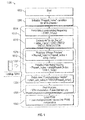
FIG. 1 is a flow chart of a pulse width modulation process according to a first embodiment; -
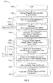
FIG. 2 is a flow chart of a pulse width modulation process according to a second embodiment; -
FIG. 3 is a flow chart of a pulse width modulation process according to a third embodiment; and -
FIG. 4 is a flow chart of a pulse width modulation process according to a fourth embodiment. - It is noted that various connections are set forth between elements in the following description and in the drawings (the contents of which are included in this disclosure by way of reference). It is noted that these connections, unless specified otherwise, may be direct or indirect and that this specification is not intended to be limiting in this respect. In this respect, a coupling between entities may refer to either a direct or an indirect connection.
- Exemplary embodiments of apparatuses, systems, and methods are described for pre-computing waveform characteristics for a single cycle of a periodic waveform and storing data points corresponding to the appropriate PWM comparator values that correspond to a given sampling instance of the waveform in a lookup table. With relatively simple operations, it is possible to derive appropriate PWM comparator values over a wide range of control or command frequency ranges just by storing the data points for a single lowest or base frequency waveform. Such techniques may be used as an alternative to, or in addition to, generating values of a control signal and a carrier signal digitally in real time using trigonometric and floating point operations or emulating floating point operations in the case of fixed point processing.
-
FIG. 1 is a flow chart of a method orprocess 1000, the start of which is denoted atblock 1002. Theprocess 1000 may be employed for both single and polyphase systems. When used for a polyphase system of N phases, theprocess 1000 keeps track of the waveform positions of each of the N phases using phase index index variables (PHASE#_INDEX). For instance, if theprocess 1000 employs a lookup table of such size (TABLE_SIZE) that has 10000 data points, that is, TABLE_SIZE=9999, for a polyphase system of three phases, theprocess 1000 may initialize or set a first phase index variable (PHASE1_INDEX) to a value of 0000, a second phase index variable (PHASE2_INDEX) to a value of 3333 and a third phase index variable (PHASE3_INDEX) to a value of 6666. The initialization may occur inblock 1006. - Following the initialization of
block 1006, theprocess 1000 then begins a repeating routine, denoted inFIG. 1 byblock 1010. The repeatingroutine 1010 may be performed or executed at a desired PWM sampling rate, such as by use of an interrupt software routine (ISR). The ISR may complete the following blocks or operations described below. - The first operation, denoted by
block 1014, is to determine a value of a variable corresponding to a desired control or command signal frequency (CMD_FREQ). This value may be at or greater than a value of a base frequency waveform, the data points of which the lookup table stores. - If the command signal frequency is greater than the frequency of the base frequency waveform, the
process 1000 then sets a value to a jump factor variable (JUMP_FACTOR) that is proportional to the command signal frequency inblock 1018. Theprocess 1000 may determine the value of the jump factor variable as the quotient of a value of the command frequency variable divided by a value representing the resolution of the lookup table (TABLE_RESOLUTION). The resolution of the lookup table determines the size of the lookup table. For instance, for a switching inverter system with a PWM carrier frequency of 10 kHz and a resolution of +/- 1 Hz, the size of the lookup table would be 10000 table data points. The same system with a resolution of +/- 10 Hz would need a lookup table of only 1000 data points. In any case, the size of the table for a system of N phases may be a multiple of N so as to maintain clear phase separation. - For each of the N phases, the
process 1000 then performs the following operations denoted withinblock 1022 and described further below. - The
process 1000 first progresses the value of the phase index variables by incrementing the value of the corresponding phase index variable by the value of the jump factor variable to establish a new value of corresponding phase index variable inblock 1026. - Optionally, the
process 1000 then handles index round tripping by modifying the value of the corresponding phase index variable to a value corresponding to the mod function of the value of the phase index variable divided by the value of the table size inblock 1030. Thisoperation 1030 increments changes in the value of the command signal frequency more smoothly. - The
process 1000 then determines the correct "commutation vector", that is, whether the PWM signal is on or off, by selecting the stored value of a PWM raw value variable (PWM_RAW_VALUE) in the lookup table that corresponds to the determined value of the phase index variable inblock 1034. - The
process 1000 then performs additional post process operations, such as V/Hz modulation, pulse deletion, and so forth, as desired inblock 1038. - After the
process 1000 completes the aforementioned operations or blocks, it loads the post-processed values of the PWM variables into PWM comparators for the switching inverter to produce the desired polyphase PWM output with N phases inblock 1042. - The embodiment of
FIG. 1 is suitable for open loop operation of a motor by the switching inverter. However, in practice there will always be a lag between the waveform of the command signal and the position of a rotor for the motor, due to slip loss, magnetic loss, mechanical friction loss, etc. -
FIG. 2 is a flow chart of a pulsewidth modulation process 2000 according to a second embodiment that incorporates a first type of error estimation (block 2002) into theprocess 2000. Theprocess 2000 is similar to theprocess 1000, so a complete re-description is omitted for the sake of brevity. - In the
process 2000 ofFIG. 2 , motor states (rotor position, speed, phase currents) are estimated by optimally reconstructing the motor states using the actual inputs (PWM sequence) and possibly any measured quantities from the motor itself. Theprocess 2000 uses the estimated motor states to derive state errors (position, speed, current) that it uses to modify the command frequency variable (CMD_FREQ) according to calculated error feedback information. Theprocess 2000 then uses the modified value of the command frequency variable to determine the value of the jump factor variable. Theprocess 2000 may receive the speed error feedback (FB) information directly using a speed or position sensor or by using a speed error estimation circuit that predicts speed error as a function of the value of the command frequency variable. The insertion of thisspeed estimator operation 2002 into theprocess 2000 optimizes the resultant waveform output of the switching inverter. -
FIG. 3 is a flow chart of a pulsewidth modulation process 3000 according to a third embodiment that incorporates a second type of error estimation (block 3002) into theprocess 3000. Theprocess 3000 is similar to theprocess 2000, so a complete re-description is omitted for the sake of brevity. - The
process 3000 estimates phase error inblock 3002 and modifies the determined value of the jump factor variable for each of N phases according to phase error feedback (FB) information. Theprocess 3000 may receive the phase error feedback information using reconstructing motor phase errors based on the actual inputs (PWM sequence) and measured quantities from the motor. Such quantities may be obtained from one or more sources, such as a position sensor. As with the case of the second embodiment described above in conjunction with theprocess 2000, the insertion of thisphase estimator operation 3002 into theprocess 3000 optimizes the resultant waveform output of the switching inverter per motor phase. - If the desired waveform from the switching inverter is symmetric, it is possible to modify one or more of the
processes FIG. 4 is a flow chart of a pulsewidth modulation process 4000 according to a fourth embodiment that keeps track of positive and negative symmetric cycles of the PWM waveform to reduce the size of the lookup table. Theprocess 4000 is similar to theprocess 1000, so a complete re-description is omitted for the sake of brevity. - The
process 4000 responds to a boolean flag that changes state between the positive and negative cycles. After the operation of progressing the value of the phase pointer variables (block 1026), theprocess 4000 uses the boolean flag to produce positive and negative cycle identification (+ve / -ve) inblock 4002. Then, after theprocess 4000 completes the operation of determining the correct "commutation vector" (block 1034), theprocess 4000 compensates the commutation vector with the correct positive or negative wave cycle according to the boolean flag identification inblock 4004. - Technical effects and benefits of this disclosure include the simplicity of implementation on a fixed or floating point processor, using a simple table indexing scheme that employs a "Jump Factor" for commanding and driving motor speed. This eliminates the need for floating point, trigonometric and complex math calculations, thereby decreasing processor load and application cost. By virtue of the simplicity it is optimized for fixed point implementation in regards to program memory and computational speed. Some embodiments may incorporate a linear/non-linear estimator that estimates the phasing error in the indexing scheme and hence optimize starting and operating torque generation for accurate motor positioning and speed profile following. Some embodiments may incorporate hardware, such as an ASIC or an FPGA.
- As described herein, in some embodiments various functions or acts may take place at a given location and/or in connection with the operation of one or more apparatuses, systems, or devices. For example, in some embodiments, a portion of a given function or act may be performed at a first device or location, and the remainder of the function or act may be performed at one or more additional devices or locations.
- Embodiments may be implemented using one or more technologies. In some embodiments, an apparatus or system may include one or more processors, and memory storing instructions that, when executed by the one or more processors, cause the apparatus or system to perform one or more methodological acts as described herein. Various mechanical components known to those of skill in the art may be used in some embodiments.
- Embodiments may be implemented as one or more apparatuses, systems, and/or methods. In some embodiments, instructions may be stored on one or more computer-readable media, such as a transitory and/or non-transitory computer-readable medium. The instructions, when executed, may cause an entity (e.g., an apparatus or system) to perform one or more methodological acts as described herein.
- Aspects of the disclosure have been described in terms of illustrative embodiments thereof. Numerous other embodiments, modifications and variations within the scope of the appended claims will occur to persons of ordinary skill in the art from a review of this disclosure. For example, one of ordinary skill in the art will appreciate that the steps described in conjunction with the illustrative figures may be performed in other than the recited order, and that one or more steps illustrated may be optional.
- The described embodiments as set forth herein represent only some illustrative implementations of the invention as set forth in the attached claims. Changes and substitutions of various details and arrangement thereof are within the scope of the claimed invention.
Claims (7)
- A method of modulating a pulse width modulation (PWM) signal, comprising:initializing at least one phase index to an initial value;establishing a set of values in a lookup table that correspond to data points for PWM comparator values that correspond to a given number of samples of a single periodic waveform during a predetermined sampling rate that establishes a table resolution;repeatedly executing the following operations at the predetermined sampling rate:determining a value of a command signal frequency;setting a value to a jump factor equal to the quotient of the value of the command signal frequency divided by the table resolution;progressing the value of the phase index by the value of the jump factor;selecting a value of a commutation vector from the lookup table that corresponds to the phase index; andloading the value of the commutation vector into a corresponding PWM comparator.
- The method of claim 1, wherein the PWM signal has N phases, and wherein the initializing of the at least one phase index to an initial value comprises initializing a number N of phase indexes to N values, and wherein the progressing of the value of the phase index, selecting the value of a commutation vector, and the loading of the value of a commutation vector occur for each of the N phases with their corresponding phase indexes.
- The method of claim 2, further comprising:modifying the value of each phase index to a value corresponding to a mod function of the value of the phase index divided by a value corresponding to a size of the table.
- The method of claim 3, further comprising:performing post-process operations on the commutation vectors.
- The method of claim 4, further comprising:compensating the determined value of the command signal frequency with speed error feedback.
- The method of claim 4, further comprising:compensating the value of the jump factor with phase error feedback.
- The method of claim 4, further comprising:identifying positive and negative cycle information from a boolean flag that changes state between positive and negative cycles after the progressing of the value of the phase index; andcompensating the commutation vector with a correct positive or negative wave cycle according to the boolean flag identification after the selecting of the value of the commutation vector.
Applications Claiming Priority (2)
| Application Number | Priority Date | Filing Date | Title |
|---|---|---|---|
| US201361810124P | 2013-04-09 | 2013-04-09 | |
| US14/200,877 US9768755B2 (en) | 2013-04-09 | 2014-03-07 | Lookup table assisted pulse width modulation |
Publications (2)
| Publication Number | Publication Date |
|---|---|
| EP2802067A1 true EP2802067A1 (en) | 2014-11-12 |
| EP2802067B1 EP2802067B1 (en) | 2018-11-07 |
Family
ID=51654031
Family Applications (1)
| Application Number | Title | Priority Date | Filing Date |
|---|---|---|---|
| EP14163684.5A Not-in-force EP2802067B1 (en) | 2013-04-09 | 2014-04-07 | Lookup table assisted pulse width modulation |
Country Status (2)
| Country | Link |
|---|---|
| US (1) | US9768755B2 (en) |
| EP (1) | EP2802067B1 (en) |
Families Citing this family (1)
| Publication number | Priority date | Publication date | Assignee | Title |
|---|---|---|---|---|
| CN105119550A (en) * | 2015-09-24 | 2015-12-02 | 杨浩东 | Simple multiphase SVPWM modulation method realized by utilization of CPLD |
Citations (2)
| Publication number | Priority date | Publication date | Assignee | Title |
|---|---|---|---|---|
| EP0316006A2 (en) * | 1987-11-12 | 1989-05-17 | Kabushiki Kaisha Toshiba | PWM controller |
| US20120032629A1 (en) * | 2010-08-06 | 2012-02-09 | Emerson Electric Co. | Electric Motor and Motor Control |
Family Cites Families (2)
| Publication number | Priority date | Publication date | Assignee | Title |
|---|---|---|---|---|
| US7012396B1 (en) * | 2004-09-30 | 2006-03-14 | Agere Systems Inc. | Increased digital spindle motor control resolution through dither |
| US8675725B2 (en) * | 2010-04-29 | 2014-03-18 | Mediatek Singapore Pte. Ltd. | Integrated circuit, communication unit and method for improved amplitude resolution of an RF-DAC |
-
2014
- 2014-03-07 US US14/200,877 patent/US9768755B2/en not_active Expired - Fee Related
- 2014-04-07 EP EP14163684.5A patent/EP2802067B1/en not_active Not-in-force
Patent Citations (2)
| Publication number | Priority date | Publication date | Assignee | Title |
|---|---|---|---|---|
| EP0316006A2 (en) * | 1987-11-12 | 1989-05-17 | Kabushiki Kaisha Toshiba | PWM controller |
| US20120032629A1 (en) * | 2010-08-06 | 2012-02-09 | Emerson Electric Co. | Electric Motor and Motor Control |
Also Published As
| Publication number | Publication date |
|---|---|
| EP2802067B1 (en) | 2018-11-07 |
| US9768755B2 (en) | 2017-09-19 |
| US20140300427A1 (en) | 2014-10-09 |
Similar Documents
| Publication | Publication Date | Title |
|---|---|---|
| CN101174811B (en) | Electric motor control method and device adopting space vector pulse width modulation | |
| US9716454B2 (en) | Driving circuit and driving method for permanent magnet synchronous motor | |
| EP3070836B1 (en) | Methods of auto tuning machine parameters and systems thereof | |
| US8583265B1 (en) | Methods, systems and apparatus for computing a voltage advance used in controlling operation of an electric machine | |
| KR20140121850A (en) | Magnetic-pole position estimation device for motor, and control apparatus using same | |
| US9774285B2 (en) | Voltage sense control circuit, voltage sense control driving circuit and driving method for permanent magnet synchronous motor | |
| RU2560090C1 (en) | Electric motor control unit with permanent magnets without position sensors | |
| JP6007511B2 (en) | Power converter | |
| KR101485989B1 (en) | Motor control device | |
| JPWO2016002744A1 (en) | Motor drive control device and signal generation method | |
| KR20140017764A (en) | Method and apparatus for obtaining maximum possible magnetic flux in permanant magnet synchronous motor | |
| Benchabane et al. | Sensorless direct torque control for salient-pole PMSM based on extended Kalman filter fed by AC/DC/AC converter | |
| US11356037B2 (en) | Inverter control device, inverter control method, inverter control program | |
| EP2802067B1 (en) | Lookup table assisted pulse width modulation | |
| US11722087B2 (en) | PWM signal measurement device, motor drive control device, PWM signal measurement method, and motor drive control method | |
| JP6569583B2 (en) | AC motor control device | |
| JP4722002B2 (en) | PWM inverter control device, PWM inverter control method, and refrigeration air conditioner | |
| CN114337389B (en) | Method, equipment and medium for predictive control of torque of brushless DC motor with hollow cup | |
| JP5186352B2 (en) | Electric motor magnetic pole position estimation device | |
| JP2015050916A (en) | Electric motor drive controller | |
| Muchande et al. | Design and implementation of a direct torque control space vector modulated three phase induction motor drive | |
| Dey et al. | Nearly constant switching frequency hysteresis current controller with fast online computation of boundary for a 2-level induction motor drive | |
| CN107787550B (en) | Method and device for controlling an electric machine using a PWM signal, and motor vehicle electric machine | |
| JP4818772B2 (en) | Inverter drive device and drive method | |
| Lin et al. | Model-free predictive current controller for four-switch three-phase inverter-fed interior permanent magnet synchronous motor drive systems |
Legal Events
| Date | Code | Title | Description |
|---|---|---|---|
| PUAI | Public reference made under article 153(3) epc to a published international application that has entered the european phase |
Free format text: ORIGINAL CODE: 0009012 |
|
| 17P | Request for examination filed |
Effective date: 20140407 |
|
| AK | Designated contracting states |
Kind code of ref document: A1 Designated state(s): AL AT BE BG CH CY CZ DE DK EE ES FI FR GB GR HR HU IE IS IT LI LT LU LV MC MK MT NL NO PL PT RO RS SE SI SK SM TR |
|
| AX | Request for extension of the european patent |
Extension state: BA ME |
|
| R17P | Request for examination filed (corrected) |
Effective date: 20150508 |
|
| RBV | Designated contracting states (corrected) |
Designated state(s): AL AT BE BG CH CY CZ DE DK EE ES FI FR GB GR HR HU IE IS IT LI LT LU LV MC MK MT NL NO PL PT RO RS SE SI SK SM TR |
|
| REG | Reference to a national code |
Ref country code: DE Ref legal event code: R079 Ref document number: 602014035446 Country of ref document: DE Free format text: PREVIOUS MAIN CLASS: H02M0007100000 Ipc: H02M0007539500 |
|
| GRAP | Despatch of communication of intention to grant a patent |
Free format text: ORIGINAL CODE: EPIDOSNIGR1 |
|
| STAA | Information on the status of an ep patent application or granted ep patent |
Free format text: STATUS: GRANT OF PATENT IS INTENDED |
|
| RIC1 | Information provided on ipc code assigned before grant |
Ipc: H03K 7/08 20060101ALI20180419BHEP Ipc: H02M 7/5395 20060101AFI20180419BHEP |
|
| INTG | Intention to grant announced |
Effective date: 20180522 |
|
| GRAS | Grant fee paid |
Free format text: ORIGINAL CODE: EPIDOSNIGR3 |
|
| GRAA | (expected) grant |
Free format text: ORIGINAL CODE: 0009210 |
|
| STAA | Information on the status of an ep patent application or granted ep patent |
Free format text: STATUS: THE PATENT HAS BEEN GRANTED |
|
| AK | Designated contracting states |
Kind code of ref document: B1 Designated state(s): AL AT BE BG CH CY CZ DE DK EE ES FI FR GB GR HR HU IE IS IT LI LT LU LV MC MK MT NL NO PL PT RO RS SE SI SK SM TR |
|
| REG | Reference to a national code |
Ref country code: GB Ref legal event code: FG4D |
|
| REG | Reference to a national code |
Ref country code: CH Ref legal event code: EP Ref country code: AT Ref legal event code: REF Ref document number: 1063277 Country of ref document: AT Kind code of ref document: T Effective date: 20181115 |
|
| REG | Reference to a national code |
Ref country code: IE Ref legal event code: FG4D |
|
| REG | Reference to a national code |
Ref country code: DE Ref legal event code: R096 Ref document number: 602014035446 Country of ref document: DE |
|
| REG | Reference to a national code |
Ref country code: NL Ref legal event code: MP Effective date: 20181107 |
|
| REG | Reference to a national code |
Ref country code: LT Ref legal event code: MG4D |
|
| REG | Reference to a national code |
Ref country code: AT Ref legal event code: MK05 Ref document number: 1063277 Country of ref document: AT Kind code of ref document: T Effective date: 20181107 |
|
| PG25 | Lapsed in a contracting state [announced via postgrant information from national office to epo] |
Ref country code: ES Free format text: LAPSE BECAUSE OF FAILURE TO SUBMIT A TRANSLATION OF THE DESCRIPTION OR TO PAY THE FEE WITHIN THE PRESCRIBED TIME-LIMIT Effective date: 20181107 Ref country code: AT Free format text: LAPSE BECAUSE OF FAILURE TO SUBMIT A TRANSLATION OF THE DESCRIPTION OR TO PAY THE FEE WITHIN THE PRESCRIBED TIME-LIMIT Effective date: 20181107 Ref country code: HR Free format text: LAPSE BECAUSE OF FAILURE TO SUBMIT A TRANSLATION OF THE DESCRIPTION OR TO PAY THE FEE WITHIN THE PRESCRIBED TIME-LIMIT Effective date: 20181107 Ref country code: LV Free format text: LAPSE BECAUSE OF FAILURE TO SUBMIT A TRANSLATION OF THE DESCRIPTION OR TO PAY THE FEE WITHIN THE PRESCRIBED TIME-LIMIT Effective date: 20181107 Ref country code: FI Free format text: LAPSE BECAUSE OF FAILURE TO SUBMIT A TRANSLATION OF THE DESCRIPTION OR TO PAY THE FEE WITHIN THE PRESCRIBED TIME-LIMIT Effective date: 20181107 Ref country code: IS Free format text: LAPSE BECAUSE OF FAILURE TO SUBMIT A TRANSLATION OF THE DESCRIPTION OR TO PAY THE FEE WITHIN THE PRESCRIBED TIME-LIMIT Effective date: 20190307 Ref country code: BG Free format text: LAPSE BECAUSE OF FAILURE TO SUBMIT A TRANSLATION OF THE DESCRIPTION OR TO PAY THE FEE WITHIN THE PRESCRIBED TIME-LIMIT Effective date: 20190207 Ref country code: LT Free format text: LAPSE BECAUSE OF FAILURE TO SUBMIT A TRANSLATION OF THE DESCRIPTION OR TO PAY THE FEE WITHIN THE PRESCRIBED TIME-LIMIT Effective date: 20181107 Ref country code: NO Free format text: LAPSE BECAUSE OF FAILURE TO SUBMIT A TRANSLATION OF THE DESCRIPTION OR TO PAY THE FEE WITHIN THE PRESCRIBED TIME-LIMIT Effective date: 20190207 |
|
| PG25 | Lapsed in a contracting state [announced via postgrant information from national office to epo] |
Ref country code: RS Free format text: LAPSE BECAUSE OF FAILURE TO SUBMIT A TRANSLATION OF THE DESCRIPTION OR TO PAY THE FEE WITHIN THE PRESCRIBED TIME-LIMIT Effective date: 20181107 Ref country code: GR Free format text: LAPSE BECAUSE OF FAILURE TO SUBMIT A TRANSLATION OF THE DESCRIPTION OR TO PAY THE FEE WITHIN THE PRESCRIBED TIME-LIMIT Effective date: 20190208 Ref country code: PT Free format text: LAPSE BECAUSE OF FAILURE TO SUBMIT A TRANSLATION OF THE DESCRIPTION OR TO PAY THE FEE WITHIN THE PRESCRIBED TIME-LIMIT Effective date: 20190307 Ref country code: NL Free format text: LAPSE BECAUSE OF FAILURE TO SUBMIT A TRANSLATION OF THE DESCRIPTION OR TO PAY THE FEE WITHIN THE PRESCRIBED TIME-LIMIT Effective date: 20181107 Ref country code: SE Free format text: LAPSE BECAUSE OF FAILURE TO SUBMIT A TRANSLATION OF THE DESCRIPTION OR TO PAY THE FEE WITHIN THE PRESCRIBED TIME-LIMIT Effective date: 20181107 Ref country code: AL Free format text: LAPSE BECAUSE OF FAILURE TO SUBMIT A TRANSLATION OF THE DESCRIPTION OR TO PAY THE FEE WITHIN THE PRESCRIBED TIME-LIMIT Effective date: 20181107 |
|
| PG25 | Lapsed in a contracting state [announced via postgrant information from national office to epo] |
Ref country code: PL Free format text: LAPSE BECAUSE OF FAILURE TO SUBMIT A TRANSLATION OF THE DESCRIPTION OR TO PAY THE FEE WITHIN THE PRESCRIBED TIME-LIMIT Effective date: 20181107 Ref country code: CZ Free format text: LAPSE BECAUSE OF FAILURE TO SUBMIT A TRANSLATION OF THE DESCRIPTION OR TO PAY THE FEE WITHIN THE PRESCRIBED TIME-LIMIT Effective date: 20181107 Ref country code: IT Free format text: LAPSE BECAUSE OF FAILURE TO SUBMIT A TRANSLATION OF THE DESCRIPTION OR TO PAY THE FEE WITHIN THE PRESCRIBED TIME-LIMIT Effective date: 20181107 Ref country code: DK Free format text: LAPSE BECAUSE OF FAILURE TO SUBMIT A TRANSLATION OF THE DESCRIPTION OR TO PAY THE FEE WITHIN THE PRESCRIBED TIME-LIMIT Effective date: 20181107 |
|
| REG | Reference to a national code |
Ref country code: DE Ref legal event code: R097 Ref document number: 602014035446 Country of ref document: DE |
|
| PG25 | Lapsed in a contracting state [announced via postgrant information from national office to epo] |
Ref country code: RO Free format text: LAPSE BECAUSE OF FAILURE TO SUBMIT A TRANSLATION OF THE DESCRIPTION OR TO PAY THE FEE WITHIN THE PRESCRIBED TIME-LIMIT Effective date: 20181107 Ref country code: SK Free format text: LAPSE BECAUSE OF FAILURE TO SUBMIT A TRANSLATION OF THE DESCRIPTION OR TO PAY THE FEE WITHIN THE PRESCRIBED TIME-LIMIT Effective date: 20181107 Ref country code: SM Free format text: LAPSE BECAUSE OF FAILURE TO SUBMIT A TRANSLATION OF THE DESCRIPTION OR TO PAY THE FEE WITHIN THE PRESCRIBED TIME-LIMIT Effective date: 20181107 Ref country code: EE Free format text: LAPSE BECAUSE OF FAILURE TO SUBMIT A TRANSLATION OF THE DESCRIPTION OR TO PAY THE FEE WITHIN THE PRESCRIBED TIME-LIMIT Effective date: 20181107 |
|
| PLBE | No opposition filed within time limit |
Free format text: ORIGINAL CODE: 0009261 |
|
| STAA | Information on the status of an ep patent application or granted ep patent |
Free format text: STATUS: NO OPPOSITION FILED WITHIN TIME LIMIT |
|
| 26N | No opposition filed |
Effective date: 20190808 |
|
| PG25 | Lapsed in a contracting state [announced via postgrant information from national office to epo] |
Ref country code: SI Free format text: LAPSE BECAUSE OF FAILURE TO SUBMIT A TRANSLATION OF THE DESCRIPTION OR TO PAY THE FEE WITHIN THE PRESCRIBED TIME-LIMIT Effective date: 20181107 |
|
| REG | Reference to a national code |
Ref country code: CH Ref legal event code: PL |
|
| REG | Reference to a national code |
Ref country code: BE Ref legal event code: MM Effective date: 20190430 |
|
| GBPC | Gb: european patent ceased through non-payment of renewal fee |
Effective date: 20190407 |
|
| PG25 | Lapsed in a contracting state [announced via postgrant information from national office to epo] |
Ref country code: MC Free format text: LAPSE BECAUSE OF FAILURE TO SUBMIT A TRANSLATION OF THE DESCRIPTION OR TO PAY THE FEE WITHIN THE PRESCRIBED TIME-LIMIT Effective date: 20181107 Ref country code: LU Free format text: LAPSE BECAUSE OF NON-PAYMENT OF DUE FEES Effective date: 20190407 |
|
| PG25 | Lapsed in a contracting state [announced via postgrant information from national office to epo] |
Ref country code: CH Free format text: LAPSE BECAUSE OF NON-PAYMENT OF DUE FEES Effective date: 20190430 Ref country code: LI Free format text: LAPSE BECAUSE OF NON-PAYMENT OF DUE FEES Effective date: 20190430 Ref country code: GB Free format text: LAPSE BECAUSE OF NON-PAYMENT OF DUE FEES Effective date: 20190407 |
|
| PG25 | Lapsed in a contracting state [announced via postgrant information from national office to epo] |
Ref country code: BE Free format text: LAPSE BECAUSE OF NON-PAYMENT OF DUE FEES Effective date: 20190430 |
|
| PG25 | Lapsed in a contracting state [announced via postgrant information from national office to epo] |
Ref country code: TR Free format text: LAPSE BECAUSE OF FAILURE TO SUBMIT A TRANSLATION OF THE DESCRIPTION OR TO PAY THE FEE WITHIN THE PRESCRIBED TIME-LIMIT Effective date: 20181107 |
|
| PG25 | Lapsed in a contracting state [announced via postgrant information from national office to epo] |
Ref country code: IE Free format text: LAPSE BECAUSE OF NON-PAYMENT OF DUE FEES Effective date: 20190407 |
|
| PG25 | Lapsed in a contracting state [announced via postgrant information from national office to epo] |
Ref country code: CY Free format text: LAPSE BECAUSE OF FAILURE TO SUBMIT A TRANSLATION OF THE DESCRIPTION OR TO PAY THE FEE WITHIN THE PRESCRIBED TIME-LIMIT Effective date: 20181107 |
|
| PG25 | Lapsed in a contracting state [announced via postgrant information from national office to epo] |
Ref country code: HU Free format text: LAPSE BECAUSE OF FAILURE TO SUBMIT A TRANSLATION OF THE DESCRIPTION OR TO PAY THE FEE WITHIN THE PRESCRIBED TIME-LIMIT; INVALID AB INITIO Effective date: 20140407 Ref country code: MT Free format text: LAPSE BECAUSE OF FAILURE TO SUBMIT A TRANSLATION OF THE DESCRIPTION OR TO PAY THE FEE WITHIN THE PRESCRIBED TIME-LIMIT Effective date: 20181107 |
|
| PGFP | Annual fee paid to national office [announced via postgrant information from national office to epo] |
Ref country code: FR Payment date: 20220323 Year of fee payment: 9 |
|
| PG25 | Lapsed in a contracting state [announced via postgrant information from national office to epo] |
Ref country code: MK Free format text: LAPSE BECAUSE OF FAILURE TO SUBMIT A TRANSLATION OF THE DESCRIPTION OR TO PAY THE FEE WITHIN THE PRESCRIBED TIME-LIMIT Effective date: 20181107 |
|
| PGFP | Annual fee paid to national office [announced via postgrant information from national office to epo] |
Ref country code: DE Payment date: 20220322 Year of fee payment: 9 |
|
| REG | Reference to a national code |
Ref country code: DE Ref legal event code: R119 Ref document number: 602014035446 Country of ref document: DE |
|
| PG25 | Lapsed in a contracting state [announced via postgrant information from national office to epo] |
Ref country code: FR Free format text: LAPSE BECAUSE OF NON-PAYMENT OF DUE FEES Effective date: 20230430 Ref country code: DE Free format text: LAPSE BECAUSE OF NON-PAYMENT OF DUE FEES Effective date: 20231103 |