EP2802046A1 - Light guiding for vertical external cavity surface emitting laser - Google Patents
Light guiding for vertical external cavity surface emitting laser Download PDFInfo
- Publication number
- EP2802046A1 EP2802046A1 EP13167055.6A EP13167055A EP2802046A1 EP 2802046 A1 EP2802046 A1 EP 2802046A1 EP 13167055 A EP13167055 A EP 13167055A EP 2802046 A1 EP2802046 A1 EP 2802046A1
- Authority
- EP
- European Patent Office
- Prior art keywords
- mesa
- layer stack
- gain layer
- mirror
- active gain
- Prior art date
- Legal status (The legal status is an assumption and is not a legal conclusion. Google has not performed a legal analysis and makes no representation as to the accuracy of the status listed.)
- Granted
Links
Images
Classifications
-
- H—ELECTRICITY
- H01—ELECTRIC ELEMENTS
- H01S—DEVICES USING THE PROCESS OF LIGHT AMPLIFICATION BY STIMULATED EMISSION OF RADIATION [LASER] TO AMPLIFY OR GENERATE LIGHT; DEVICES USING STIMULATED EMISSION OF ELECTROMAGNETIC RADIATION IN WAVE RANGES OTHER THAN OPTICAL
- H01S5/00—Semiconductor lasers
- H01S5/10—Construction or shape of the optical resonator, e.g. extended or external cavity, coupled cavities, bent-guide, varying width, thickness or composition of the active region
- H01S5/18—Surface-emitting [SE] lasers, e.g. having both horizontal and vertical cavities
- H01S5/183—Surface-emitting [SE] lasers, e.g. having both horizontal and vertical cavities having only vertical cavities, e.g. vertical cavity surface-emitting lasers [VCSEL]
- H01S5/18308—Surface-emitting [SE] lasers, e.g. having both horizontal and vertical cavities having only vertical cavities, e.g. vertical cavity surface-emitting lasers [VCSEL] having a special structure for lateral current or light confinement
-
- H—ELECTRICITY
- H01—ELECTRIC ELEMENTS
- H01S—DEVICES USING THE PROCESS OF LIGHT AMPLIFICATION BY STIMULATED EMISSION OF RADIATION [LASER] TO AMPLIFY OR GENERATE LIGHT; DEVICES USING STIMULATED EMISSION OF ELECTROMAGNETIC RADIATION IN WAVE RANGES OTHER THAN OPTICAL
- H01S5/00—Semiconductor lasers
- H01S5/10—Construction or shape of the optical resonator, e.g. extended or external cavity, coupled cavities, bent-guide, varying width, thickness or composition of the active region
- H01S5/18—Surface-emitting [SE] lasers, e.g. having both horizontal and vertical cavities
- H01S5/183—Surface-emitting [SE] lasers, e.g. having both horizontal and vertical cavities having only vertical cavities, e.g. vertical cavity surface-emitting lasers [VCSEL]
- H01S5/18344—Surface-emitting [SE] lasers, e.g. having both horizontal and vertical cavities having only vertical cavities, e.g. vertical cavity surface-emitting lasers [VCSEL] characterized by the mesa, e.g. dimensions or shape of the mesa
-
- H—ELECTRICITY
- H01—ELECTRIC ELEMENTS
- H01S—DEVICES USING THE PROCESS OF LIGHT AMPLIFICATION BY STIMULATED EMISSION OF RADIATION [LASER] TO AMPLIFY OR GENERATE LIGHT; DEVICES USING STIMULATED EMISSION OF ELECTROMAGNETIC RADIATION IN WAVE RANGES OTHER THAN OPTICAL
- H01S5/00—Semiconductor lasers
- H01S5/10—Construction or shape of the optical resonator, e.g. extended or external cavity, coupled cavities, bent-guide, varying width, thickness or composition of the active region
- H01S5/18—Surface-emitting [SE] lasers, e.g. having both horizontal and vertical cavities
- H01S5/183—Surface-emitting [SE] lasers, e.g. having both horizontal and vertical cavities having only vertical cavities, e.g. vertical cavity surface-emitting lasers [VCSEL]
- H01S5/18397—Plurality of active layers vertically stacked in a cavity for multi-wavelength emission
-
- H—ELECTRICITY
- H01—ELECTRIC ELEMENTS
- H01S—DEVICES USING THE PROCESS OF LIGHT AMPLIFICATION BY STIMULATED EMISSION OF RADIATION [LASER] TO AMPLIFY OR GENERATE LIGHT; DEVICES USING STIMULATED EMISSION OF ELECTROMAGNETIC RADIATION IN WAVE RANGES OTHER THAN OPTICAL
- H01S5/00—Semiconductor lasers
- H01S5/30—Structure or shape of the active region; Materials used for the active region
- H01S5/32—Structure or shape of the active region; Materials used for the active region comprising PN junctions, e.g. hetero- or double- heterostructures
- H01S5/3222—Structure or shape of the active region; Materials used for the active region comprising PN junctions, e.g. hetero- or double- heterostructures in AIVBVI compounds, e.g. PbSSe-laser
-
- H—ELECTRICITY
- H01—ELECTRIC ELEMENTS
- H01S—DEVICES USING THE PROCESS OF LIGHT AMPLIFICATION BY STIMULATED EMISSION OF RADIATION [LASER] TO AMPLIFY OR GENERATE LIGHT; DEVICES USING STIMULATED EMISSION OF ELECTROMAGNETIC RADIATION IN WAVE RANGES OTHER THAN OPTICAL
- H01S5/00—Semiconductor lasers
- H01S5/40—Arrangement of two or more semiconductor lasers, not provided for in groups H01S5/02 - H01S5/30
- H01S5/42—Arrays of surface emitting lasers
- H01S5/423—Arrays of surface emitting lasers having a vertical cavity
- H01S5/426—Vertically stacked cavities
-
- H—ELECTRICITY
- H01—ELECTRIC ELEMENTS
- H01S—DEVICES USING THE PROCESS OF LIGHT AMPLIFICATION BY STIMULATED EMISSION OF RADIATION [LASER] TO AMPLIFY OR GENERATE LIGHT; DEVICES USING STIMULATED EMISSION OF ELECTROMAGNETIC RADIATION IN WAVE RANGES OTHER THAN OPTICAL
- H01S2301/00—Functional characteristics
- H01S2301/16—Semiconductor lasers with special structural design to influence the modes, e.g. specific multimode
- H01S2301/166—Single transverse or lateral mode
-
- H—ELECTRICITY
- H01—ELECTRIC ELEMENTS
- H01S—DEVICES USING THE PROCESS OF LIGHT AMPLIFICATION BY STIMULATED EMISSION OF RADIATION [LASER] TO AMPLIFY OR GENERATE LIGHT; DEVICES USING STIMULATED EMISSION OF ELECTROMAGNETIC RADIATION IN WAVE RANGES OTHER THAN OPTICAL
- H01S2301/00—Functional characteristics
- H01S2301/17—Semiconductor lasers comprising special layers
- H01S2301/176—Specific passivation layers on surfaces other than the emission facet
-
- H—ELECTRICITY
- H01—ELECTRIC ELEMENTS
- H01S—DEVICES USING THE PROCESS OF LIGHT AMPLIFICATION BY STIMULATED EMISSION OF RADIATION [LASER] TO AMPLIFY OR GENERATE LIGHT; DEVICES USING STIMULATED EMISSION OF ELECTROMAGNETIC RADIATION IN WAVE RANGES OTHER THAN OPTICAL
- H01S5/00—Semiconductor lasers
- H01S5/04—Processes or apparatus for excitation, e.g. pumping, e.g. by electron beams
- H01S5/041—Optical pumping
-
- H—ELECTRICITY
- H01—ELECTRIC ELEMENTS
- H01S—DEVICES USING THE PROCESS OF LIGHT AMPLIFICATION BY STIMULATED EMISSION OF RADIATION [LASER] TO AMPLIFY OR GENERATE LIGHT; DEVICES USING STIMULATED EMISSION OF ELECTROMAGNETIC RADIATION IN WAVE RANGES OTHER THAN OPTICAL
- H01S5/00—Semiconductor lasers
- H01S5/10—Construction or shape of the optical resonator, e.g. extended or external cavity, coupled cavities, bent-guide, varying width, thickness or composition of the active region
- H01S5/14—External cavity lasers
-
- H—ELECTRICITY
- H01—ELECTRIC ELEMENTS
- H01S—DEVICES USING THE PROCESS OF LIGHT AMPLIFICATION BY STIMULATED EMISSION OF RADIATION [LASER] TO AMPLIFY OR GENERATE LIGHT; DEVICES USING STIMULATED EMISSION OF ELECTROMAGNETIC RADIATION IN WAVE RANGES OTHER THAN OPTICAL
- H01S5/00—Semiconductor lasers
- H01S5/40—Arrangement of two or more semiconductor lasers, not provided for in groups H01S5/02 - H01S5/30
- H01S5/42—Arrays of surface emitting lasers
- H01S5/423—Arrays of surface emitting lasers having a vertical cavity
Definitions
- the present invention relates to an active gain layer stack according to the preamble of claim 1 and to a laser device comprising two mirrors forming a cavity and said active gain layer stack. Moreover, the present invention relates to method of operation of said laser device and a method of fabrication of said active gain layer stack.
- Semiconductor lasers for the mid-infrared are known since the 1970s.
- the original devices are edge emitters, pumped electrically in the form of a laser diode, have to be cooled cryogenically and depending on design emitt in a spectral range from 2 micrometers to 20 micrometers wavelength. This range will in the following be called the "mid-IR" range.
- narrow gap IV-VI semiconductors like PbSnTe, PbEuTe, PbSrTe, where Te may be fully or partially replaced by Se or S in various compositions, were used.
- III-V based lasers using semiconductors like GaAs, GaSb, InP or InSb and compounds thereof were developed for the mid-infrared, too.
- QCL quantum and interband cascade laser diodes
- ICL edge emitters
- Their spectral range covers wavelengths from about 3 micrometers up to larger than 20 micrometers.
- QCL and ICL need a sophisticated layered structure, consisting of many hundreds of semiconductor layers grown monolithically on III-V substrates. Some of these designs operate up to room temperature and in continuous wave.
- edge emitting laser diodes are their strong astigmatic emission beam with a very high divergence angle, e.g. 60°, in one direction.
- a very high divergence angle e.g. 60°
- the large aperture in one direction is due to the very thin layers of the gain structure in order to keep a threshold current low.
- VECSEL Vertical Cavity Surface Emitting Laser
- VCSEL are often electrically pumped.
- the current is guided through the active region using a so called buried tunnel junction. It is essentially an etched structure with a diameter of multiple micrometers which is later overgrown with the second mirror.
- an additional structuring on top of the active region is used to suppress higher order transversal modes by inducing losses.
- Optically pumped VECSEL have advantages in the construction to obtain high beam quality, low losses and high power.
- the diameter of a pumping spot needs to be aligned with a cavity mode spot and is in a range of few to multiple hundred micrometers.
- a curved external mirror can be used for better definition of the laser mode diameter, which depends on cavity length, mirror curvature, and emission mode order.
- VCSEL as well as VECSEL are commonly used e.g. for telecommunication applications. While VCSEL are limited to low power applications, very high powers have been reached with VECSEL.
- VECSEL For VECSEL based on III-V semiconductors, the longest laser mid-IR wavelengths are below 2.8 micrometers. VECSEL using IV-VI materials may, however, cover the whole mid-infrared range. Such devices were described in M. Fill, F. Felder, M. Rahim, A. Khiar, R. Rodriguez, H. Zogg, A. Ishida, IV-VI mid-infrared VECSEL on Si-substrate, Proc. SPIE, 82420H, 2012. IV-VI VECSEL are especially important for infrared spectroscopy, where a narrow, monochromatic and wavelength tunable illumination is required. Such a device is described in M. Rahim, A. Khiar, M. Fill, F. Felder, H.
- Such tunable VECSEL may be used in a whole range of different applications.
- One such application is, e.g., trace gas spectroscopy for environmental monitoring.
- Other applications include trace gas, gas, or liquid spectroscopy for industrial process control or medical diagnosis of severe diseases.
- Combustion gases and hydrocarbons have very strong absorption lines at mid-infrared wavelengths from 3 ⁇ m to 10 ⁇ m.
- Gas spectroscopy sensors therefore offer a very high sensitivity when operating within this wavelength region.
- the mid-IR laser modules allow to harvest the full potential of spectroscopic sensors.
- Other applications include medical surgery (tissue cutting or healing), material processing, or military countermeasures.
- There are two transparency windows in the mid-infrared 3-5 ⁇ m and 8-14 ⁇ m), where atmospheric absorption is minimal. This allows reliable signal transmission over long distances, i.e . free space communications.
- an active gain layer stack for a vertical emitting laser device comprising a semiconductor material and being structured such that it forms at least one mesa extending in a vertical direction and a transversally neighboring region at least partly surrounding said mesa, wherein at least part of said mesa has a first refractive index and wherein a part of the neighboring region transversally adjacent to said part of the mesa has second refractive index, wherein said first refractive index is higher than said second refractive index, and wherein a diameter in transversal direction of said mesa is chosen such that a transversal confinement factor in the active gain layer stack is increased, wherein said semiconductor material has a refractive index that decreases with increasing temperature.
- the diameter in transversal direction of said mesa is chosen such that a transversal confinement of the laser light in the active gain layer stack is increased.
- the vertical direction is the direction substantially perpendicular to the active gain layer stack surface, i.e. the direction in which the laser light is emitted, whereas the transversal or horizontal direction is parallel to the active gain layer stack surface.
- mesa is to be understood as a protrusion in vertical direction from a gain layer stack surface, from a mirror, or from a substrate, depending on the height (or depth) of the mesa.
- Said protrusion has a substantially flat distal surface and steep edges.
- the distal surface is the top surface of the mesa.
- a mesa may have a longitudinal cross section with a substantially rectangular or trapezoidal shape, wherein the distal surface in case of trapezoidal shape may be provided on the small or on the larger of the two parallel sides of the trapezoid.
- the mesa may also have a mushroom- or a pear-shaped cross section. Typical heights of a mesa are similar to the thickness of the active gain layer, or more e.g.
- a plurality of mesas may be arranged in a preferably regular pattern on the gain layer stack surface, on the mirror, or on the substrate. If the mesa is provided on the substrate, the mesa preferably but not necessarily comprises a mirror layer opposite the distal surface of the mesa.
- said semiconductor material is a IV-VI semiconductor material, such as PbSnTe, PbEuTe, PbSrTe, where Te may be fully or partially replaced by Se or S.
- IV-VI semiconductor material such as PbSnTe, PbEuTe, PbSrTe, where Te may be fully or partially replaced by Se or S.
- Preferred compositions of said materials consist i.e. of Pb 1-x Sr x Te, where x is in the range of 0 % up to 15%.
- Lead salts are preferred materials.
- the active gain layer stack or package comprises a semiconductor material having a first refractive index and forming on its surface at least one transversally thereon extending lasing spot.
- the lasing spot is preferably at least part of or the entire distal surface of the mesa.
- the gain layer stack further comprises a lasing spot region, given by the mesa body and preferably the active region extending below the mesa body.
- the gain layer stack further comprises a substrate on which the active region is provided on. The substrate provides support.
- the active lasing spot region extends with its height substantially vertical from said lasing spot into said active gain layer stack, wherein the lasing spot region includes said lasing spot, and wherein said semiconductor material is a IV-VI semiconductor material, wherein a first refractive index of at least a part of the lasing spot region is higher than a second refractive index of a neighboring region of the active gain layer stack transversally adjacent to and encompassing said part of the lasing spot region, thus increasing a transversal confinement factor in the active gain layer stack.
- the threshold gain required to operate a V(E)CSEL depends on the modal confinement factor, which has components in the horizontal plane.
- this confinement factor is close to unity thanks to a favorable temperature-dependence of the refractive index of the materials. Pumping the laser results in a temperature gradient and thus a refractive index gradient from a center of the emission spot outward occurs, resulting in a guiding structure for the laser light.
- the temperature-dependence when using IV-VI materials is, however, inverse and the refractive index increases with lower temperatures. In such an anti-guided structure the electric field diverges into the outer part where the refractive index is higher.
- the transverse confinement factor is by orders of magnitude smaller, resulting in a significantly increased lasing threshold and degraded device efficiency.
- the refractive index of Pb 0 . 95 Sr 0 . 05 Te increases about 1% towards the rim of the lasing spot.
- the active gain layer stack according to invention may be included in an active gain region of a vertical emitting laser (e.g . a VECSEL or a VCSEL).
- a vertical emitting laser e.g . a VECSEL or a VCSEL.
- the present invention achieves an advantageous light guiding effect by confining the lasing mode in horizontal, i.e . transversal, direction.
- the refractive index gradient or its spatial dependence is effectively inverted, with a high refractive index in the center of the active lasing spot region, in particular of the lasing spot and a low refractive index at the edge and outside of the active lasing spot region and the lasing spot, respectively.
- the laser mode is then concentrated spatially in the regime with high refractive index. This increased confinement factor significantly reduces the threshold power of the laser, resulting in a much improved power efficiency.
- Devices using this invention can be operated at higher temperatures and with a higher duty cycle or even continuously.
- Using spatially defined lasing spots has additional advantages in the later implementation and adds to the lasing characteristics. Just a single lasing spot can be fabricated in order to accurately and uniquely define the position at which laser light is generated. This is of importance in applications where the light path needs to be known precisely, or for simplified optical alignment. Using multiple lasing spots in close proximity simultaneously for light generation yields a higher total output power. Furthermore, the lasing properties can be tuned, for example to achieve different emission wavelengths, by switching between different lasing spots.
- the presented invention significantly advances the IV-VI laser technology by increasing the wall-plug efficiency and allowing different operation modes:
- the neighboring region of the active gain layer stack surrounding a mesa as described above includes at least one of:
- Vacuum and gas have a refractive index of about 1, resulting in a very large contrast of a factor of up to about 6 compared to the mesa itself.
- Liquids including water or solvents typically have a refractive index of about 1.3 to 1.5. In case of a solid region surrounding the mesa, the contrast of refractive index is much smaller depending on the material and the fabrication method used. Typical values range from multiple % for suited IV-VI material compositions up to a factor of 4 for silicon oxides.
- the neighboring region may thus be in a first direction a solid material, wherein in a second direction perpendicular to the first direction it may be provided by a vacuum or a gas region.
- the neighboring region surrounds said mesa over substantially the entire vertically extending height of said mesa and preferably encircles said mesa transversally completely.
- the active gain layer stack as described above is structured such as to provide on its surface at least one vertically extending mesa, wherein each one mesa forms a lasing spot region with a lasing spot on its distal surface.
- the lasing spot region may extend further below the mesa into the active gain layer stack, preferably down to the substrate.
- at least part of said substrate acts as a mirror.
- a mesa may extends vertically into the direction pointing away from a substrate carrying the active gain layer package, or it may extend vertically into the direction pointing toward said substrate.
- the neighboring region around the mesa may be filled with a desired material or pumped empty to a vacuum region.
- the neighboring region around the mesa may be the same basic material as the mesa is made from, wherein the material of the neighboring region is treated such as to have a lower refractive index, i.e . through ion implantation, irradiation or other techniques.
- the height of the lasing spot region i.e. the mesa as described above, is substantially equal to or smaller than a height of the active gain layer stack.
- the height of the lasing spot region or the mesa as described above extends substantially vertically down to a substrate, whereupon the active gain layer stack is directly or indirectly provided on.
- a vertical extension down to the substrate is particularly advantageous, if the active gain layer stack is manufactured by an etching process, as the substrate, typically made from silicon, may act as an etch stop.
- the mesa may have a rotational symmetry with the rotation axis pointing in vertical direction.
- the lateral surface or the edges of the mesa may, however, be undercut such that a mushroom-like shape results or it may be inclined, such that the lateral surface has a substantially cone- or pear-shaped form.
- the lasing spot region has a round cross section, wherein said round cross section is preferably of a substantially part-circular or circular shape, or wherein the lasing spot region has a cornered cross section.
- a diameter of the lasing spot region or the lasing spot or the mesa in transversal direction is preferably in a range extending from 5 to 500 micrometers, in particular from 20 to 100 micrometers and in particular of about 40 micrometers.
- Realized devices consist of mesa with a height of about 1 micrometer and diameters of about 40 micrometers suited for a lasing spot size corresponding to a cavity length of about 60 micrometers.
- the diameter of the mesa is chosen such that higher order transversal modes are suppressed.
- the active gain layer stack has a plurality of individual of said lasing spot regions or mesas, wherein these individual lasing spot regions have the same or different emission characteristics.
- a vertical emitting laser device including a first mirror with at least one first mirror layer, with a second mirror with at least one second mirror layer forming an optical cavity with said first mirror, and with an active region between the first and the second mirror, characterized in that said active region includes at least one active gain layer stack as described above.
- the cavity formed by the two mirrors is arranged with a length in order that only one single longitudinal laser mode is emitted whose wavelength may be shifted mode-hop-free by altering the cavity length.
- the cavity length may be long, resulting in multi-mode emission or single-mode emission using an additional optical element within the cavity.
- the laser is fabricated using IV-VI materials and emits in the mid-infrared range of the electromagnetic spectrum. It preferably is optically pumped, but the presented invention is useful for electric pumping of the gain medium as well.
- said active gain layer stack is provided on the first mirror, wherein a height of the mesa in vertical direction is equal to or at least 10% to 100% percent of a height of said active gain layer stack, i.e. the active gain layer is provided as individual mesas. More preferably said height of the mesa in vertical direction is larger than said height of said active gain layer stack, such that the mesa extends through or over the active gain layer stack into the first mirror.
- each mesa comprises an active gain layer and a mirror.
- the mesa layer closest to the substrate is a mirror layer, wherein the transversally neighboring part of the mesa mirror layer is part of the neighboring region as described above. Hence the mesa is provided on the remaining part of the mirror.
- the mesa extends in vertical direction through or over the entire active gain layer stack and first mirror onto or into a substrate whereupon the first mirror is provided on.
- the mesa comprises a mirror layer.
- the mesa can also extend into or comprise part of the substrate, such that the proximal mesa layer is made from substrate material.
- the active laser stack according to invention may be described in the following way.
- a basic structure one has either (a) a substrate, on the surface of which the active gain layers are directly provided on, or (b) a substrate, whereupon a mirror is provided, wherein the active gain layers are provided on the surface of said mirror.
- the active gain layer stack may not include a mirror layer (situation (a)) or may include a mesa mirror layer (situation (b)).
- each mesa may include, in vertical direction:
- the variants (i) to (vi) may be achieved by building up layer by layer (material deposition processes) or by removing layer by layer from the basic structure (e.g. etching processes) or by applying both these techniques.
- the etch stop may conveniently be chosen in the active gain layer stack, on or in the mirror layer, or on or in the substrate layer.
- the mirror or the substrate in general can act as a natural etch stop layer, which makes the fabrication of the device simpler.
- the laser device is constructed such that a diameter of the mesa in transversal direction is substantially equal to or slightly larger than a cavity mode spot size of a TEM00 mode.
- the vertical emitting laser device may be used or operated by pumping one or at least one lasing spot region or mesa.
- This pumping may be an optical or an electrical pumping, wherein each distal surface of a pumped mesa forms an active lasing spot.
- a plurality of lasing spots regions is pumped simultaneously or consecutively.
- all lasing spots of one lasing area are lasing with comparable threshold, output powers, and wavelengths.
- emission wavelengths are different for individual lasing spots.
- the efficiency gains presented in this invention can be fully utilized while multiplying the output power or achieving a broader emission spectrum or wavelength tuning range.
- Simultaneous emission of multiple lasing spots is achieved by simply pumping multiple lasing spot regions. For consecutive pumping the threshold power is exceeded only for one lasing spot region at a time, i.e. by moving the pumping light over individual spots.
- the vertical emitting laser device as mentioned above is operated by applying a switching between different lasing regimes during operation.
- the laser device is manufactured on a wafer level or individually for a chip.
- Due to material properties the invention is specific to lasers using IV-VI semiconductors in the active region, both optically and electrically pumped. While structuring of the active region has been used extensively for various reasons, to our best knowledge no etched structure has been designed to create a light guiding structure in the described context. Commonly used wave guides rely on total reflection at the interfaces, which is of no importance here.
- a VECSEL-type laser device may be broadly defined as follows:
- a VECSEL-type laser is a surface-emitting semiconductor laser having a first ("bottom") mirror and a second ("top") mirror which is disposed at a distance from the first mirror, forming an optical cavity with the first mirror.
- An active region (gain medium) comprising at least one active semiconductor layer is disposed in the cavity, the semiconductor layer being oriented such that the resulting laser beam in the cavity will be substantially perpendicular to the layer plane.
- the active region may optionally comprise quantum wells or quantum dots.
- the active region contains regions (lasing area) fabricated in such a way, that the refractive index within this region remains higher than its surroundings during operation of the laser. The area where lasing is possible may be limited by macroscopic parts, such as a sample mount.
- the first and/or the second mirror serve as an output coupler for an output beam.
- the laser may be optically or electrically pumped.
- the lasing spots are typically round, but other shapes may be chosen for different reasons including better heat flux, selection of one or more specific transversal modes, polarization selection of the emitted light, or passivation.
- Their size is chosen to be approximately at the minimum of threshold power.
- the lasing threshold decreases with smaller size and thus stronger confinement, but increases for to small diameters as additional losses are induced.
- the optimal size depends on multiple parameters of the cavity such as its optical length and the curvatures of the mirrors. With decreasing cavity length and increasing curvature the size becomes smaller, down to a few micrometers.
- the manufacturing may be done on wafer level or individually for smaller chips. In both cases one or more lasing spots with uniform or individual properties are placed at the area where lasing will occur. Typically a symmetric repetitive arrangement of multiple lasing spots is chosen for each such lasing area.
- a shadow mask is used to structure the active region.
- the mask or a slightly larger one can also be used on any number of beforehand deposited layers, including partial layers and layers forming a mirror.
- lasing spots are etched after growth using standard lithography and etching techniques. The etch depth can be through any number of layers, including partial layers and layers forming a mirror, down to the substrate.
- the size of the etched structure can be slightly larger in the mirror layers.
- the low refractive material can be either using vacuum or any gas mixture including air.
- the space around the lasing spot can also be filled with other materials with a refractive index lower than the IV-VI semiconductors used in the active region, for example to improve the heat removal from the active region. In both cases, a passivation of the vertical walls of the lasing spot may be applied.
- the refractive index gradient structure may also be produced by changing the composition of the IV-VI semiconductor layers using ion implementation at selected areas.
- Either flat or curved mirrors can be used.
- flat mirrors aligned substantially parallel, all lasing spots of one lasing area are lasing with comparable threshold, output powers, and wavelengths.
- emission wavelengths are different for individual lasing spots.
- lasing characteristics for the individual lasing spots differ, too. The lowest threshold is achieved for the one lasing spot where the mirror curvature aligns optimal with the laser cavity.
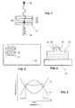
- a first preferred embodiment of a VECSEL according to the present invention is schematically illustrated in Figures 1 and 2 . It is to be noted that the dimensions are not to scale. In particular, the thickness of the individual parts of the laser along the vertical direction is strongly exaggerated in relation to the dimensions in the horizontal plane, in order to illustrate the sequence of layers in the laser device.
- a VECSEL 10 consisting of a first mirror 11, a second mirror 12 and a gain layer region 13, and an external cavity 14.
- the active gain layer region 13 is provided on the second mirror 12. It may alternatively be provided on the first mirror 11.
- the mirrors 11, 12 are highly reflective for the laser emission wavelength and are realized using well known technologies, e.g. metallic coatings or distributed Bragg reflectors on suitable substrates.
- the active region 13 consists of IV-VI semiconductor materials as commonly used in laser devices. It is structured with lasing spots 22 standing out of a surface 23, and grouped within the lasing area 31.
- the schematic refractive index profile over a lasing spot 22 and its close surroundings changes from a normal IV-VI gradient 32 to the induced profile 33, as shown in figure 3 .
- Also shown in figure 3 is the refractive index gradient 31 for III-V semiconductor materials for comparison.
- Figs. 1 and 2 are just examples. Either of the two mirrors may be flat (planar) or curved. As the spot diameter of the cavity mode on the active region is typically below about 0.1 mm, the lasing spot layout may be made very compact. In addition, a single lasing spot is sufficient for lasing. A total device size of below about 1 x 1 x 1 mm3 is possible.
- An example of a concrete set-up realized in the laboratory uses 5 x 5 mm 2 lasing area.
- the active region was grown epitaxially directly on the first mirror.
- the curved second mirror was positioned in approximately 50 micrometer distance.
- the lasing spots and lasing spot regions were created using wet etching. Lasing spot sizes or mesa diameters in transversal direction are the range of 5 to 500 micrometers, preferably sizes of about 40 micrometers were chosen, in relation to the mirror curvature of 100 mm and the cavity length.
- the device was optically pumped using a commercial 1.55 ⁇ m laser diode, operated in pulsed mode at 20 kHz repetition rate and with 10 ns pulse width, and recorded with a Fourier transform infrared spectrometer.
- the threshold power is reduced at least by a factor of five.
- Peak output power is approximately 10 mWp, limited by the power of the pumping diode.
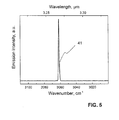
- the emission wavelength depends on operating temperature and cavity length. Fig. 5 shows an example of such laser emission spectrum 41.
- Figure 4 shows a schematic sketch of a cross section of an active gain layer stack 21 with a mesa 24 extending in vertical direction (upwards direction in Fig. 4 ) and having a first refractive index n 1 .
- a multi-layer structure is indicated by the broken lines.
- the distal surface 22 in vertical direction of the mesa 24 forms the lasing spot 22 during lasing action, i.e. if the mesa 24 is pumped.
- the mesa 24 is surrounded transversally completely by an adjacent neighboring region 25 with a lower second refractive index n 2 , here a gas or vacuum.
- the spatial variation of the refractive index follows the curve 33 in Fig. 3 , where the jump continuities in curve 33 correspond to the transversal edge of the mesa 24.
- a plurality of mesas 24 are provided on the gain layer stack or package 21, wherein the plurality of mesas 24 is preferably arranged in a regular pattern with typical transversal distances (i.e. edge-to-edge clearance) between next neighboring mesas 24 in the order of a 1 micrometer up to 200 micrometers.
- Figure 5 shows an output spectrum of a VECSEL in accordance with the setup of the previous figures.
- LIST OF REFERENCE SIGNS 11 first mirror 32 Refractive index in IV-VI semiconductor materials during operation 12 second mirror 13 active region 14 external cavity 33 Refractive index in IV-VI semiconductor materials during operation achieved by this invention 15 pump laser light in 16 generated laser light out 21 active gain layer stack, possibly with mirror below 41 emission spectrum 22 lasing spot 23 substrate n 1 first refractive index 24 lasing spot region 25 neighbor region to 24 n 2 second refractive index 31 Refractive index in III-V semiconductor materials during operation
Landscapes
- Physics & Mathematics (AREA)
- Condensed Matter Physics & Semiconductors (AREA)
- General Physics & Mathematics (AREA)
- Electromagnetism (AREA)
- Optics & Photonics (AREA)
- Semiconductor Lasers (AREA)
Abstract
Description
- The present invention relates to an active gain layer stack according to the preamble of claim 1 and to a laser device comprising two mirrors forming a cavity and said active gain layer stack. Moreover, the present invention relates to method of operation of said laser device and a method of fabrication of said active gain layer stack.
- Semiconductor lasers for the mid-infrared are known since the 1970s. The original devices are edge emitters, pumped electrically in the form of a laser diode, have to be cooled cryogenically and depending on design emitt in a spectral range from 2 micrometers to 20 micrometers wavelength. This range will in the following be called the "mid-IR" range. As semiconductor material, narrow gap IV-VI semiconductors like PbSnTe, PbEuTe, PbSrTe, where Te may be fully or partially replaced by Se or S in various compositions, were used. Later, III-V based lasers using semiconductors like GaAs, GaSb, InP or InSb and compounds thereof were developed for the mid-infrared, too. Again, these are typically laser diodes pumped electrically and edge-emitting. Wavelengths up to about 3.5 micrometers are reached. As an alternative, quantum and interband cascade laser diodes (QCL, ICL), again edge emitters, have proven to be useful. Their spectral range covers wavelengths from about 3 micrometers up to larger than 20 micrometers. QCL and ICL need a sophisticated layered structure, consisting of many hundreds of semiconductor layers grown monolithically on III-V substrates. Some of these designs operate up to room temperature and in continuous wave.
- The disadvantage of edge emitting laser diodes is their strong astigmatic emission beam with a very high divergence angle, e.g. 60°, in one direction. To focus or collimate this beam to one with Gaussian-like shape, sophisticated and expensive optical elements are needed and a considerable part of the output power is lost. The large aperture in one direction is due to the very thin layers of the gain structure in order to keep a threshold current low.
- Much is gained if the semiconductor laser emits vertically with respect to the surface. With a typical beam exit diameter of at least several to tens of micrometers, a narrow circular output cone results with an opening angle of a few degrees only. Such lasers exhibit a "good beam quality" emission in a quasi-perfect radial-symmetric Gaussian shape with very small divergence angles, e.g. below 2°, and with a beam quality factor M2 approaching unity. Contrarily, the factor M2 is much higher in edge emitting lasers. Such Vertical Cavity Surface Emitting Laser (VCSEL), also called semiconductor disk laser, are fabricated monolithically or, for higher powers, with an external cavity. The latter are consequently called Vertical External Cavity Surface Emitting Laser (VECSEL). VCSEL are often electrically pumped. In order to achieve sufficient high currents above threshold level, the current is guided through the active region using a so called buried tunnel junction. It is essentially an etched structure with a diameter of multiple micrometers which is later overgrown with the second mirror. In some cases of electrically pumped VECSEL an additional structuring on top of the active region is used to suppress higher order transversal modes by inducing losses. Optically pumped VECSEL have advantages in the construction to obtain high beam quality, low losses and high power. The diameter of a pumping spot needs to be aligned with a cavity mode spot and is in a range of few to multiple hundred micrometers. A curved external mirror can be used for better definition of the laser mode diameter, which depends on cavity length, mirror curvature, and emission mode order. VCSEL as well as VECSEL are commonly used e.g. for telecommunication applications. While VCSEL are limited to low power applications, very high powers have been reached with VECSEL.
- For VECSEL based on III-V semiconductors, the longest laser mid-IR wavelengths are below 2.8 micrometers. VECSEL using IV-VI materials may, however, cover the whole mid-infrared range. Such devices were described in M. Fill, F. Felder, M. Rahim, A. Khiar, R. Rodriguez, H. Zogg, A. Ishida, IV-VI mid-infrared VECSEL on Si-substrate, Proc. SPIE, 82420H, 2012. IV-VI VECSEL are especially important for infrared spectroscopy, where a narrow, monochromatic and wavelength tunable illumination is required. Such a device is described in M. Rahim, A. Khiar, M. Fill, F. Felder, H. Zogg, Continuously tunable single mode VECSEL at 3.3 µm wavelength for spectroscopy, Electron. Lett. 47, 18, p.1037-1039, 2011. The wavelength tuning range extends from about 3.2 to 3.3 micrometers. The beam is single mode monochromatic, and tuning is completely mode-hop free.
- Such tunable VECSEL may be used in a whole range of different applications. One such application is, e.g., trace gas spectroscopy for environmental monitoring. Other applications include trace gas, gas, or liquid spectroscopy for industrial process control or medical diagnosis of severe diseases. Combustion gases and hydrocarbons have very strong absorption lines at mid-infrared wavelengths from 3 µm to 10 µm. Gas spectroscopy sensors therefore offer a very high sensitivity when operating within this wavelength region. By making the whole mid-infrared accessible, the mid-IR laser modules allow to harvest the full potential of spectroscopic sensors. Other applications include medical surgery (tissue cutting or healing), material processing, or military countermeasures. There are two transparency windows in the mid-infrared (3-5 µm and 8-14 µm), where atmospheric absorption is minimal. This allows reliable signal transmission over long distances, i.e. free space communications.
- Current lasers based on IV-VI semiconductors cannot be operated efficiently. With IV-VI materials the temperature-dependence of the refractive index leads to a strong anti-guiding effect on the generated laser light. This temperature-dependence is a fundamental physical property and cannot be influenced. The anti-guiding effect results in a significantly increased lasing threshold. As a consequence, the devices cannot be operated at the desired high temperatures, require higher pumping power, or emit lower output power. Those aspects increase the complexity of the packaging, add unnecessary costs, and make the laser's use in an application more difficult and less reliable.
- It is therefore an object of the present invention to provide an active gain layer stack that overcomes the aforementioned disadvantages and improves the wall-plug efficiency of vertical emitting lasers in particular based on IV-VI semiconductors, independently of whether they are electrically or optically pumped.
- This and other objects are achieved by providing an active gain layer stack for a vertical emitting laser device, the active gain layer stack comprising a semiconductor material and being structured such that it forms at least one mesa extending in a vertical direction and a transversally neighboring region at least partly surrounding said mesa, wherein at least part of said mesa has a first refractive index and wherein a part of the neighboring region transversally adjacent to said part of the mesa has second refractive index, wherein said first refractive index is higher than said second refractive index, and wherein a diameter in transversal direction of said mesa is chosen such that a transversal confinement factor in the active gain layer stack is increased, wherein said semiconductor material has a refractive index that decreases with increasing temperature.
- In other words, the diameter in transversal direction of said mesa is chosen such that a transversal confinement of the laser light in the active gain layer stack is increased.
- The vertical direction is the direction substantially perpendicular to the active gain layer stack surface, i.e. the direction in which the laser light is emitted, whereas the transversal or horizontal direction is parallel to the active gain layer stack surface.
- The term "mesa" is to be understood as a protrusion in vertical direction from a gain layer stack surface, from a mirror, or from a substrate, depending on the height (or depth) of the mesa. Said protrusion has a substantially flat distal surface and steep edges. The distal surface is the top surface of the mesa. A mesa may have a longitudinal cross section with a substantially rectangular or trapezoidal shape, wherein the distal surface in case of trapezoidal shape may be provided on the small or on the larger of the two parallel sides of the trapezoid. The mesa may also have a mushroom- or a pear-shaped cross section. Typical heights of a mesa are similar to the thickness of the active gain layer, or more e.g. in case of additional layers between the active gain layer and the substrate, and may even reach multiple micrometers into the substrate. Preferably, a plurality of mesas may be arranged in a preferably regular pattern on the gain layer stack surface, on the mirror, or on the substrate. If the mesa is provided on the substrate, the mesa preferably but not necessarily comprises a mirror layer opposite the distal surface of the mesa.
- According to a preferred embodiment, said semiconductor material is a IV-VI semiconductor material, such as PbSnTe, PbEuTe, PbSrTe, where Te may be fully or partially replaced by Se or S. Preferred compositions of said materials consist i.e. of Pb1-xSrxTe, where x is in the range of 0 % up to 15%. Lead salts are preferred materials.
- Preferably, the active gain layer stack or package comprises a semiconductor material having a first refractive index and forming on its surface at least one transversally thereon extending lasing spot. The lasing spot is preferably at least part of or the entire distal surface of the mesa. The gain layer stack further comprises a lasing spot region, given by the mesa body and preferably the active region extending below the mesa body. The gain layer stack further comprises a substrate on which the active region is provided on. The substrate provides support. The active lasing spot region extends with its height substantially vertical from said lasing spot into said active gain layer stack, wherein the lasing spot region includes said lasing spot, and wherein said semiconductor material is a IV-VI semiconductor material, wherein a first refractive index of at least a part of the lasing spot region is higher than a second refractive index of a neighboring region of the active gain layer stack transversally adjacent to and encompassing said part of the lasing spot region, thus increasing a transversal confinement factor in the active gain layer stack.
- It is important to realize here, that the threshold gain required to operate a V(E)CSEL, and thus its energy efficiency, depends on the modal confinement factor, which has components in the horizontal plane. In the case of III-V materials, this confinement factor is close to unity thanks to a favorable temperature-dependence of the refractive index of the materials. Pumping the laser results in a temperature gradient and thus a refractive index gradient from a center of the emission spot outward occurs, resulting in a guiding structure for the laser light. The temperature-dependence when using IV-VI materials is, however, inverse and the refractive index increases with lower temperatures. In such an anti-guided structure the electric field diverges into the outer part where the refractive index is higher. The transverse confinement factor is by orders of magnitude smaller, resulting in a significantly increased lasing threshold and degraded device efficiency.
- Said difference from the first to the second refractive index is present in particular during operation of the gain layer stack, i.e. while the active lasing spot region is at operation temperature. For a temperature gradient of 30°C from the center of the lasing spot with maximum heating, the refractive index of Pb0.95Sr0.05Te increases about 1% towards the rim of the lasing spot.
- The active gain layer stack according to invention may be included in an active gain region of a vertical emitting laser (e.g. a VECSEL or a VCSEL).
- The present invention achieves an advantageous light guiding effect by confining the lasing mode in horizontal, i.e. transversal, direction. Using etched or expitaxially grown structures or spatially differing material compositions or structures, the refractive index gradient or its spatial dependence is effectively inverted, with a high refractive index in the center of the active lasing spot region, in particular of the lasing spot and a low refractive index at the edge and outside of the active lasing spot region and the lasing spot, respectively. The laser mode is then concentrated spatially in the regime with high refractive index. This increased confinement factor significantly reduces the threshold power of the laser, resulting in a much improved power efficiency. Devices using this invention can be operated at higher temperatures and with a higher duty cycle or even continuously.
- Using spatially defined lasing spots has additional advantages in the later implementation and adds to the lasing characteristics. Just a single lasing spot can be fabricated in order to accurately and uniquely define the position at which laser light is generated. This is of importance in applications where the light path needs to be known precisely, or for simplified optical alignment. Using multiple lasing spots in close proximity simultaneously for light generation yields a higher total output power. Furthermore, the lasing properties can be tuned, for example to achieve different emission wavelengths, by switching between different lasing spots.
- The presented invention significantly advances the IV-VI laser technology by increasing the wall-plug efficiency and allowing different operation modes:
- Due to the significantly increased efficiency, the devices can be built much smaller. No heat sink is necessary at all and uncooled operation is possible. This allows the successful use in applications in which even small amounts of waste heat are undesired. The stability of the whole system is improved, resulting in a more reliable integration.
- New applications become possible due to the more versatile design possibilities regarding output power and an exact definition of the emission spot. Advanced devices allow a switching between different lasing regimes during operation.
- Continuous wave emission becomes possible for operation close to room temperature, even in a simple setup using thermoelectric stabilization.
- Preferably, the neighboring region of the active gain layer stack surrounding a mesa as described above includes at least one of:
- a vacuum region, or
- a gas-filled region, or
- a liquid-filled region, or
- a solid region, wherein a material of said solid region has a lower refractive index than the refractive index of said part of the lasing spot region.
- Vacuum and gas have a refractive index of about 1, resulting in a very large contrast of a factor of up to about 6 compared to the mesa itself. Liquids including water or solvents typically have a refractive index of about 1.3 to 1.5. In case of a solid region surrounding the mesa, the contrast of refractive index is much smaller depending on the material and the fabrication method used. Typical values range from multiple % for suited IV-VI material compositions up to a factor of 4 for silicon oxides.
- As an example, the neighboring region may thus be in a first direction a solid material, wherein in a second direction perpendicular to the first direction it may be provided by a vacuum or a gas region.
- According to a preferred embodiment of the invention, the neighboring region surrounds said mesa over substantially the entire vertically extending height of said mesa and preferably encircles said mesa transversally completely.
- According to another preferred embodiment, the active gain layer stack as described above is structured such as to provide on its surface at least one vertically extending mesa, wherein each one mesa forms a lasing spot region with a lasing spot on its distal surface. The lasing spot region may extend further below the mesa into the active gain layer stack, preferably down to the substrate. Preferably, at least part of said substrate acts as a mirror.
- It is to be understood, that a mesa may extends vertically into the direction pointing away from a substrate carrying the active gain layer package, or it may extend vertically into the direction pointing toward said substrate. In the former case, the neighboring region around the mesa may be filled with a desired material or pumped empty to a vacuum region. In the latter case, the neighboring region around the mesa may be the same basic material as the mesa is made from, wherein the material of the neighboring region is treated such as to have a lower refractive index, i.e. through ion implantation, irradiation or other techniques.
- Preferably, the height of the lasing spot region, i.e. the mesa as described above, is substantially equal to or smaller than a height of the active gain layer stack. According to a preferred embodiment, the height of the lasing spot region or the mesa as described above extends substantially vertically down to a substrate, whereupon the active gain layer stack is directly or indirectly provided on. A vertical extension down to the substrate is particularly advantageous, if the active gain layer stack is manufactured by an etching process, as the substrate, typically made from silicon, may act as an etch stop.
- In vertical direction, the mesa may have a rotational symmetry with the rotation axis pointing in vertical direction. The lateral surface or the edges of the mesa may, however, be undercut such that a mushroom-like shape results or it may be inclined, such that the lateral surface has a substantially cone- or pear-shaped form.
- According to a preferred embodiment, the lasing spot region has a round cross section, wherein said round cross section is preferably of a substantially part-circular or circular shape, or wherein the lasing spot region has a cornered cross section.
- A diameter of the lasing spot region or the lasing spot or the mesa in transversal direction is preferably in a range extending from 5 to 500 micrometers, in particular from 20 to 100 micrometers and in particular of about 40 micrometers. Realized devices consist of mesa with a height of about 1 micrometer and diameters of about 40 micrometers suited for a lasing spot size corresponding to a cavity length of about 60 micrometers.
- Preferably, the diameter of the mesa is chosen such that higher order transversal modes are suppressed.
- According to yet another preferred embodiment, the active gain layer stack has a plurality of individual of said lasing spot regions or mesas, wherein these individual lasing spot regions have the same or different emission characteristics.
- It is another object of the present invention to provide a vertical emitting laser device with improved wall-plug efficiency.
- This object is achieved by a vertical emitting laser device including a first mirror with at least one first mirror layer, with a second mirror with at least one second mirror layer forming an optical cavity with said first mirror, and with an active region between the first and the second mirror, characterized in that said active region includes at least one active gain layer stack as described above.
- Preferably, the cavity formed by the two mirrors is arranged with a length in order that only one single longitudinal laser mode is emitted whose wavelength may be shifted mode-hop-free by altering the cavity length. Alternatively, the cavity length may be long, resulting in multi-mode emission or single-mode emission using an additional optical element within the cavity. The laser is fabricated using IV-VI materials and emits in the mid-infrared range of the electromagnetic spectrum. It preferably is optically pumped, but the presented invention is useful for electric pumping of the gain medium as well.
- In a particularly preferred embodiment said active gain layer stack is provided on the first mirror, wherein a height of the mesa in vertical direction is equal to or at least 10% to 100% percent of a height of said active gain layer stack, i.e. the active gain layer is provided as individual mesas. More preferably said height of the mesa in vertical direction is larger than said height of said active gain layer stack, such that the mesa extends through or over the active gain layer stack into the first mirror. This means that each mesa comprises an active gain layer and a mirror.
- In this case, the mesa layer closest to the substrate is a mirror layer, wherein the transversally neighboring part of the mesa mirror layer is part of the neighboring region as described above. Hence the mesa is provided on the remaining part of the mirror.
- More preferably, the mesa extends in vertical direction through or over the entire active gain layer stack and first mirror onto or into a substrate whereupon the first mirror is provided on. In this case, the mesa comprises a mirror layer. The mesa can also extend into or comprise part of the substrate, such that the proximal mesa layer is made from substrate material.
- Preferred embodiments of the active laser stack according to invention may be described in the following way. As a basic structure one has either (a) a substrate, on the surface of which the active gain layers are directly provided on, or (b) a substrate, whereupon a mirror is provided, wherein the active gain layers are provided on the surface of said mirror. Alternatively, one could say the active gain layer stack may not include a mirror layer (situation (a)) or may include a mesa mirror layer (situation (b)).
- The mesa structure is worked into this basic structure (a) or (b) such that each mesa may include, in vertical direction:
- (i) only a part of the active gain layers (i.e. mesa height smaller than active gain layer stack height, mesa is provided on the active gain layers);
- (ii) the entire gain layers (i.e. mesa height substantially equal to active gain layer stack height; the mesa is provided on a substrate, which substrate can be a mirror);
- (iii & iv) the entire gain layer stack, and, if no mirror is provided for (situation (a)), a part of the substrate or, if a mirror is provided (situation (b)), a part of said mirror;
- (v) the entire gain layer stack and the entire mirror, if a mirror is provided for (situation (b));
- (vi) the entire gain layer stack and the entire mirror and a part of the substrate, if a mirror is provided for (situation (b)).
- The variants (i) to (vi) may be achieved by building up layer by layer (material deposition processes) or by removing layer by layer from the basic structure (e.g. etching processes) or by applying both these techniques.
- If one produces the mesa by means of an etching technology, the etch stop may conveniently be chosen in the active gain layer stack, on or in the mirror layer, or on or in the substrate layer.
- The mirror or the substrate in general can act as a natural etch stop layer, which makes the fabrication of the device simpler.
- Preferably the laser device is constructed such that a diameter of the mesa in transversal direction is substantially equal to or slightly larger than a cavity mode spot size of a TEM00 mode.
- The vertical emitting laser device may be used or operated by pumping one or at least one lasing spot region or mesa. This pumping may be an optical or an electrical pumping, wherein each distal surface of a pumped mesa forms an active lasing spot.
- According to a preferred embodiment, a plurality of lasing spots regions is pumped simultaneously or consecutively. In case of substantially parallel mirror alignment, all lasing spots of one lasing area are lasing with comparable threshold, output powers, and wavelengths. In case of deviation from perfect parallelism, i.e. when a curved mirror is used, emission wavelengths are different for individual lasing spots. In both cases the efficiency gains presented in this invention can be fully utilized while multiplying the output power or achieving a broader emission spectrum or wavelength tuning range. In the latter case, Simultaneous emission of multiple lasing spots is achieved by simply pumping multiple lasing spot regions. For consecutive pumping the threshold power is exceeded only for one lasing spot region at a time, i.e. by moving the pumping light over individual spots.
- Preferably, the vertical emitting laser device as mentioned above is operated by applying a switching between different lasing regimes during operation.
- It is yet another object of the present invention to provide a method of manufacturing an active gain layer as described above.
- This and other objects are achieved by a method of manufacturing of said active gain layer stack or said laser device, in that the active gain layer stack is manufactured by applying etching techniques or by applying epitaxial growth techniques.
- Using this method, the laser device is manufactured on a wafer level or individually for a chip.
- It is an aspect of the present invention to use a structured active region to effectively ensure a higher refractive index where lasing occurs and thus confine the laser mode to this spacial region in order to improve device efficiency. Due to material properties the invention is specific to lasers using IV-VI semiconductors in the active region, both optically and electrically pumped. While structuring of the active region has been used extensively for various reasons, to our best knowledge no etched structure has been designed to create a light guiding structure in the described context. Commonly used wave guides rely on total reflection at the interfaces, which is of no importance here.
- Preferred embodiments of the invention are described in the following with reference to the drawings, which are for the purpose of illustrating the present preferred embodiments of the invention and not for the purpose of limiting the same. In the drawings,
- Fig. 1
- shows a schematic sketch of a typical embodiment of the laser;
- Fig. 2
- shows a typical arrangement of lasing spots for a lasing area;
- Fig. 3
- shows the refractive index gradient for III-V and IV-VI semiconductor materials during a laser pulse;
- Fig. 4
- shows a schematic sketch of a mesa provided on the active gain layer stack according to
Fig. 2 ; and - Fig. 5
- shows a diagram containing an output spectrum of a VECSEL in accordance with the setup of the previous figures.
- For the purposes of the present invention, a VECSEL-type laser device may be broadly defined as follows: A VECSEL-type laser is a surface-emitting semiconductor laser having a first ("bottom") mirror and a second ("top") mirror which is disposed at a distance from the first mirror, forming an optical cavity with the first mirror. An active region (gain medium) comprising at least one active semiconductor layer is disposed in the cavity, the semiconductor layer being oriented such that the resulting laser beam in the cavity will be substantially perpendicular to the layer plane. The active region may optionally comprise quantum wells or quantum dots. The active region contains regions (lasing area) fabricated in such a way, that the refractive index within this region remains higher than its surroundings during operation of the laser. The area where lasing is possible may be limited by macroscopic parts, such as a sample mount. The first and/or the second mirror serve as an output coupler for an output beam. The laser may be optically or electrically pumped.
- The lasing spots are typically round, but other shapes may be chosen for different reasons including better heat flux, selection of one or more specific transversal modes, polarization selection of the emitted light, or passivation. Their size is chosen to be approximately at the minimum of threshold power. The lasing threshold decreases with smaller size and thus stronger confinement, but increases for to small diameters as additional losses are induced. The optimal size depends on multiple parameters of the cavity such as its optical length and the curvatures of the mirrors. With decreasing cavity length and increasing curvature the size becomes smaller, down to a few micrometers.
- The manufacturing may be done on wafer level or individually for smaller chips. In both cases one or more lasing spots with uniform or individual properties are placed at the area where lasing will occur. Typically a symmetric repetitive arrangement of multiple lasing spots is chosen for each such lasing area. During epitaxial deposition of the light generating IV-VI semiconductors a shadow mask is used to structure the active region. The mask or a slightly larger one can also be used on any number of beforehand deposited layers, including partial layers and layers forming a mirror. Alternatively, lasing spots are etched after growth using standard lithography and etching techniques. The etch depth can be through any number of layers, including partial layers and layers forming a mirror, down to the substrate. The size of the etched structure can be slightly larger in the mirror layers. The low refractive material can be either using vacuum or any gas mixture including air. The space around the lasing spot can also be filled with other materials with a refractive index lower than the IV-VI semiconductors used in the active region, for example to improve the heat removal from the active region. In both cases, a passivation of the vertical walls of the lasing spot may be applied. The refractive index gradient structure may also be produced by changing the composition of the IV-VI semiconductor layers using ion implementation at selected areas.
- Either flat or curved mirrors can be used. In case of flat mirrors, aligned substantially parallel, all lasing spots of one lasing area are lasing with comparable threshold, output powers, and wavelengths. In case of deviation from perfect parallelism, or when a curved mirror is used, emission wavelengths are different for individual lasing spots. In case of a curved mirror, lasing characteristics for the individual lasing spots differ, too. The lowest threshold is achieved for the one lasing spot where the mirror curvature aligns optimal with the laser cavity.
- A first preferred embodiment of a VECSEL according to the present invention is schematically illustrated in
Figures 1 and 2 . It is to be noted that the dimensions are not to scale. In particular, the thickness of the individual parts of the laser along the vertical direction is strongly exaggerated in relation to the dimensions in the horizontal plane, in order to illustrate the sequence of layers in the laser device. AVECSEL 10 consisting of afirst mirror 11, asecond mirror 12 and again layer region 13, and anexternal cavity 14. The activegain layer region 13 is provided on thesecond mirror 12. It may alternatively be provided on thefirst mirror 11. Themirrors active region 13 consists of IV-VI semiconductor materials as commonly used in laser devices. It is structured withlasing spots 22 standing out of asurface 23, and grouped within thelasing area 31. The schematic refractive index profile over alasing spot 22 and its close surroundings changes from a normal IV-VI gradient 32 to the inducedprofile 33, as shown infigure 3 . Also shown infigure 3 is therefractive index gradient 31 for III-V semiconductor materials for comparison. - The layouts in
Figs. 1 and 2 are just examples. Either of the two mirrors may be flat (planar) or curved. As the spot diameter of the cavity mode on the active region is typically below about 0.1 mm, the lasing spot layout may be made very compact. In addition, a single lasing spot is sufficient for lasing. A total device size of below about 1 x 1 x 1 mm3 is possible. - An example of a concrete set-up realized in the laboratory uses 5 x 5 mm2 lasing area. The active region was grown epitaxially directly on the first mirror. The curved second mirror was positioned in approximately 50 micrometer distance. The lasing spots and lasing spot regions were created using wet etching. Lasing spot sizes or mesa diameters in transversal direction are the range of 5 to 500 micrometers, preferably sizes of about 40 micrometers were chosen, in relation to the mirror curvature of 100 mm and the cavity length. The device was optically pumped using a commercial 1.55 µm laser diode, operated in pulsed mode at 20 kHz repetition rate and with 10 ns pulse width, and recorded with a Fourier transform infrared spectrometer. Compared to devices without defined lasing spots, the threshold power is reduced at least by a factor of five. Peak output power is approximately 10 mWp, limited by the power of the pumping diode. The emission wavelength depends on operating temperature and cavity length.
Fig. 5 shows an example of suchlaser emission spectrum 41. -
Figure 4 shows a schematic sketch of a cross section of an activegain layer stack 21 with amesa 24 extending in vertical direction (upwards direction inFig. 4 ) and having a first refractive index n 1. A multi-layer structure is indicated by the broken lines. Thedistal surface 22 in vertical direction of themesa 24 forms thelasing spot 22 during lasing action, i.e. if themesa 24 is pumped. Themesa 24 is surrounded transversally completely by an adjacent neighboringregion 25 with a lower second refractive index n 2, here a gas or vacuum. The difference of the refractive indices n 1 and n 2 at working temperature, i.e. while themesa 24 is lasing, is such that a transversal confinement factor in the activegain layer stack 21 is enhanced in comparison to the situation, where the activegain layer stack 21 does not have a neighboring region with a lower refractive index n 2 as described above. The spatial variation of the refractive index follows thecurve 33 inFig. 3 , where the jump continuities incurve 33 correspond to the transversal edge of themesa 24. By having such a spatially varying refractive index, the mesa-structuring ofgain layer stack 21 overcomes the disadvantage of the anti-guiding effect known from the state of the art. The activegain layer stack 21 is provided on asubstrate 23 and well suited for use in a VECSEL or VCSEL. - Preferably, a plurality of
mesas 24 are provided on the gain layer stack orpackage 21, wherein the plurality ofmesas 24 is preferably arranged in a regular pattern with typical transversal distances (i.e. edge-to-edge clearance) between nextneighboring mesas 24 in the order of a 1 micrometer up to 200 micrometers. -
Figure 5 shows an output spectrum of a VECSEL in accordance with the setup of the previous figures.LIST OF REFERENCE SIGNS 11 first mirror 32 Refractive index in IV-VI semiconductor materials during operation 12 second mirror 13 active region 14 external cavity 33 Refractive index in IV-VI semiconductor materials during operation achieved by this invention 15 pump laser light in 16 generated laser light out 21 active gain layer stack, possibly with mirror below 41 emission spectrum 22 lasing spot 23 substrate n 1 first refractive index 24 lasing spot region 25 neighbor region to 24 n 2 second refractive index 31 Refractive index in III-V semiconductor materials during operation
Claims (15)
- An active gain layer stack (21) for a vertical emitting laser device, the active gain layer stack (21) comprising a semiconductor material, characterized in that
the active gain layer stack (21) is structured such that it forms at least one mesa (24) extending in a vertical direction and
a transversally neighboring region (25) at least partly surrounding said mesa (24),
wherein at least part of said mesa (24) has a first refractive index (n 1) and wherein a part of the neighboring region (25) transversally adjacent to said part of the mesa (24) has a second refractive index (n 2), wherein said first refractive index (n 1) is higher than said second refractive index (n 2), and
in that a diameter in transversal direction of said mesa (24) is chosen such that a transversal confinement factor in the active gain layer stack (21) is increased, wherein said semiconductor material has a refractive index (n 1) that decreases with increasing temperature. - The active gain layer stack (21) according to claim 1, wherein the semiconductor material is a IV-VI semiconductor material.
- The active gain layer stack (21) according to claim 1 or 2, wherein said neighboring region (25) includes at least one of:- a vacuum region,- a gas-filled region,- a liquid-filled region, and- a solid region, wherein a material of said solid region has a lower refractive index (n 2) than the refractive index (n 1) of said part of the mesa (24).
- The active gain layer stack (21) according to any one of claims 1 to 3, wherein the neighboring region (25) surrounds said mesa (24) over substantially the entire vertically extending height of said mesa (24), and preferably encircles said mesa (24) transversally completely.
- The active gain layer stack (21) according any one of claims 1 to 4, wherein the vertically extending height of the mesa (24) is substantially equal to or smaller than a height of the active gain layer stack (21).
- The active gain layer stack (21) according any one of claims 1 to 4, wherein the active gain layer stack (21) includes a substrate (11;23), wherein the vertically extending height of the mesa (24) extends substantially down onto or into said substrate (11;23), wherein preferably, at least part of said substrate (11;23) acts as a mirror (11).
- The active gain layer stack (21) according to any one of claims 1 to 6, wherein the diameter of the mesa (24) in transversal direction is in a range extending from 5 to 500 micrometers.
- The active gain layer stack (21) according any one of claims 1 to 7, wherein the active gain layer stack (21) has a plurality of individual said mesas (24), wherein these individual mesas (24) have the same or different emission characteristics.
- A method of manufacturing of the active gain layer stack (21) according to any one claim 1 to 8, characterized in that the active gain layer stack (21) is manufactured by applying etching techniques or by locally changing the material properties after epitaxial growth.
- A vertical emitting laser device including a first mirror (11) with at least one first mirror layer, a second mirror (12) with at least one second mirror layer forming an optical cavity with said first mirror (11), and an active region (13) between the first and the second mirror (11,12), characterized in that said active region (13) includes at least one active gain layer stack (21) according to any one of the preceding claims.
- The vertical emitting laser device according to claim 10, wherein said active gain layer stack (21) is provided on the first mirror (11), wherein a height of the mesa (24) in vertical direction is at least 10% to 100% percent of a height of said active gain layer stack (21), wherein preferably said height of the mesa (24) in vertical direction is larger than said height of the active gain layer stack (21), such that the mesa (24) extends over the height of the active gain layer stack (21) into the first mirror (11), such that the mesa (24) comprises a mirror layer, wherein more preferably, the mesa (24) extends in vertical direction over the entire height of the active gain layer stack (21) and the first mirror (11) onto or into a substrate (23) whereupon the first mirror (11) is provided on, such that the mesa (24) comprises the gain layer stack (21) and a mirror layer or it comprises the gain layer stack (21), a mirror layer, and a substrate layer.
- The vertical emitting laser device according to claim 10 or 11, wherein a diameter of the mesa (24) in transversal direction is substantially equal to a cavity mode spot size of a TEM00 mode.
- The method of manufacturing according to claims 10 or 11, wherein the diameter and form of the mesa (24) is chosen such that only selected transversal modes are lasing.
- A method of operation of the vertical emitting laser device according to claim 11, 12 or 13, wherein said laser device is operated by pumping one or at least one mesa (24), wherein each distal surface of a pumped mesa (24) forms an active lasing spot.
- The method of operation according to claim 14, wherein a plurality of mesas (24) is pumped simultaneously or consecutively, and/or wherein the vertical emitting laser device is operated by applying a switching between different lasing regimes during operation.
Priority Applications (4)
| Application Number | Priority Date | Filing Date | Title |
|---|---|---|---|
| EP13167055.6A EP2802046B1 (en) | 2013-05-08 | 2013-05-08 | Light guiding for vertical external cavity surface emitting laser |
| PCT/EP2014/059022 WO2014180751A1 (en) | 2013-05-08 | 2014-05-04 | Light guiding for vertical external cavity surface emitting laser |
| US14/787,493 US9859686B2 (en) | 2013-05-08 | 2014-05-04 | Light guiding for vertical external cavity surface emitting laser |
| JP2016512307A JP2016518031A (en) | 2013-05-08 | 2014-05-04 | Light guiding for vertical external cavity surface emitting lasers |
Applications Claiming Priority (1)
| Application Number | Priority Date | Filing Date | Title |
|---|---|---|---|
| EP13167055.6A EP2802046B1 (en) | 2013-05-08 | 2013-05-08 | Light guiding for vertical external cavity surface emitting laser |
Publications (2)
| Publication Number | Publication Date |
|---|---|
| EP2802046A1 true EP2802046A1 (en) | 2014-11-12 |
| EP2802046B1 EP2802046B1 (en) | 2022-11-23 |
Family
ID=48325467
Family Applications (1)
| Application Number | Title | Priority Date | Filing Date |
|---|---|---|---|
| EP13167055.6A Active EP2802046B1 (en) | 2013-05-08 | 2013-05-08 | Light guiding for vertical external cavity surface emitting laser |
Country Status (4)
| Country | Link |
|---|---|
| US (1) | US9859686B2 (en) |
| EP (1) | EP2802046B1 (en) |
| JP (1) | JP2016518031A (en) |
| WO (1) | WO2014180751A1 (en) |
Families Citing this family (2)
| Publication number | Priority date | Publication date | Assignee | Title |
|---|---|---|---|---|
| US11275202B1 (en) * | 2017-11-28 | 2022-03-15 | Facebook Technologies, Llc | GRIN lens structure in micro-LED devices |
| CN110112653B (en) * | 2019-06-20 | 2023-11-14 | 海南师范大学 | Vertical external cavity surface emitting semiconductor laser |
Citations (1)
| Publication number | Priority date | Publication date | Assignee | Title |
|---|---|---|---|---|
| JPS609187A (en) * | 1983-06-29 | 1985-01-18 | Fujitsu Ltd | Semiconductor light-emitting device |
Family Cites Families (12)
| Publication number | Priority date | Publication date | Assignee | Title |
|---|---|---|---|---|
| JPS5831307A (en) * | 1981-08-20 | 1983-02-24 | Tokyo Optical Co Ltd | interference filter |
| JPH0750807B2 (en) * | 1984-03-28 | 1995-05-31 | 東北大学長 | Junction type semiconductor light emitting device |
| FR2671238B1 (en) * | 1990-12-28 | 1993-03-12 | Thomson Csf | METHOD FOR PRODUCING SURFACE EMITTING SEMICONDUCTOR LASERS, AND LASERS OBTAINED BY THE PROCESS. |
| US6277696B1 (en) * | 1995-06-27 | 2001-08-21 | Hewlett-Packard Company | Surface emitting laser using two wafer bonded mirrors |
| US6031858A (en) * | 1996-09-09 | 2000-02-29 | Kabushiki Kaisha Toshiba | Semiconductor laser and method of fabricating same |
| JP3472177B2 (en) * | 1998-02-25 | 2003-12-02 | 日本電信電話株式会社 | Manufacturing method of vertical cavity type semiconductor laser device and vertical cavity type semiconductor laser |
| US6643305B2 (en) * | 2000-04-07 | 2003-11-04 | The United States Of America As Represented By The Secretary Of The Navy | Optical pumping injection cavity for optically pumped devices |
| US6795478B2 (en) * | 2002-03-28 | 2004-09-21 | Applied Optoelectronics, Inc. | VCSEL with antiguide current confinement layer |
| DE102006024220A1 (en) * | 2006-04-13 | 2007-10-18 | Osram Opto Semiconductors Gmbh | Optoelectronic semiconductor component |
| JP2009283888A (en) * | 2008-02-12 | 2009-12-03 | Ricoh Co Ltd | Surface emitting laser element, surface emitting laser array, optical scanning device, and image forming apparatus |
| JP2012216664A (en) * | 2011-03-31 | 2012-11-08 | Furukawa Electric Co Ltd:The | Laser element, laser element array, light source and optical module |
| JP2013074002A (en) * | 2011-09-27 | 2013-04-22 | Sony Corp | Light emitting device and manufacturing method thereof |
-
2013
- 2013-05-08 EP EP13167055.6A patent/EP2802046B1/en active Active
-
2014
- 2014-05-04 WO PCT/EP2014/059022 patent/WO2014180751A1/en not_active Ceased
- 2014-05-04 JP JP2016512307A patent/JP2016518031A/en active Pending
- 2014-05-04 US US14/787,493 patent/US9859686B2/en not_active Expired - Fee Related
Patent Citations (1)
| Publication number | Priority date | Publication date | Assignee | Title |
|---|---|---|---|---|
| JPS609187A (en) * | 1983-06-29 | 1985-01-18 | Fujitsu Ltd | Semiconductor light-emitting device |
Non-Patent Citations (5)
| Title |
|---|
| CHANG-HASNAIN C J ET AL: "TRANSVERSE MODE CHARACTERISTICS OF VERTICAL CAVITY SURFACE-EMITTING LASERS", APPLIED PHYSICS LETTERS, AIP, AMERICAN INSTITUTE OF PHYSICS, MELVILLE, NY, US, vol. 57, no. 3, 16 July 1990 (1990-07-16), pages 218 - 220, XP000150083, ISSN: 0003-6951, DOI: 10.1063/1.103743 * |
| FILL M ET AL: "PbSe quantum well mid-infrared vertical external cavity surface emitting laser on Si-substrates", JOURNAL OF APPLIED PHYSICS, AMERICAN INSTITUTE OF PHYSICS. NEW YORK, US, vol. 109, no. 9, 2 May 2011 (2011-05-02), pages 93101 - 93101, XP012148996, ISSN: 0021-8979, DOI: 10.1063/1.3579450 * |
| M. FILL; F. FELDER; M. RAHIM; A. KHIAR; R. RODRIGUEZ; H. ZOGG; A. ISHIDA: "IV-VI mid-infrared VECSEL on Si-substrate", PROC. SPIE, 82420H, 2012 |
| M. RAHIM; A. KHIAR; M. FILL; F. FELDER; H. ZOGG: "Continuously tunable single mode VECSEL at 3.3 µm wavelength for spectroscopy", ELECTRON. LETT., vol. 47, no. 18, 2011, pages 1037 - 1039 |
| SPRINGHOLZ G ET AL: "Molecular beam epitaxy of lead salt-based vertical cavity surface emitting lasers for the 4-6 mum spectral region", JOURNAL OF CRYSTAL GROWTH, ELSEVIER, AMSTERDAM, NL, vol. 227-228, 1 July 2001 (2001-07-01), pages 722 - 728, XP004250927, ISSN: 0022-0248, DOI: 10.1016/S0022-0248(01)00810-7 * |
Also Published As
| Publication number | Publication date |
|---|---|
| WO2014180751A1 (en) | 2014-11-13 |
| US9859686B2 (en) | 2018-01-02 |
| JP2016518031A (en) | 2016-06-20 |
| US20160104998A1 (en) | 2016-04-14 |
| EP2802046B1 (en) | 2022-11-23 |
Similar Documents
| Publication | Publication Date | Title |
|---|---|---|
| Hirose et al. | Watt-class high-power, high-beam-quality photonic-crystal lasers | |
| US9438011B2 (en) | Single-mode, distributed feedback interband cascade lasers | |
| US8396091B2 (en) | Device comprising a laser | |
| Kang et al. | DFB laser diodes based on GaN using 10th order laterally coupled surface gratings | |
| US8964796B2 (en) | Structure for electron-beam pumped edge-emitting device and methods for producing same | |
| US20130250986A1 (en) | Optically pumped surface emitting lasers incorporating high reflectivity/ bandwidth limited reflector | |
| TW201342755A (en) | Surface emitting multiwavelength distributed-feedback concentric ring lasers | |
| US20230163571A1 (en) | Quantum cascade laser with high efficiency operation and related systems and methods | |
| JP5775093B2 (en) | High power quantum cascade laser with active photonic crystal structure | |
| CN101390263B (en) | semiconductor laser device | |
| US20200328574A1 (en) | Increase VCSEL Power Using Multiple Gain Layers | |
| US9543731B2 (en) | Method and device for generating short optical pulses | |
| US20120230358A1 (en) | High-power quantum cascade lasers with active-photonic-crystal structure for single, in-phase mode operation | |
| US9859686B2 (en) | Light guiding for vertical external cavity surface emitting laser | |
| US10958041B2 (en) | Method for making a semiconductor laser diode, and laser diode | |
| US10243330B2 (en) | Optoelectronic device with resonant suppression of high order optical modes and method of making same | |
| Lutsenko et al. | Optically pumped quantum-dot Cd (Zn) Se/ZnSe laser and microchip converter for yellow–green spectral region | |
| US20170317472A1 (en) | Optoelectronic device with enhanced lateral leakage of high order transverse optical modes into alloy-intermixed regions and method of making same | |
| JP2006162736A (en) | Terahertz wave generator | |
| EP2913903B1 (en) | Device comprising a high brightness broad-area edge-emitting semiconductor laser and method of making the same | |
| Kristjánsson et al. | Circular grating-coupled surface-emitter with high-quality focused output beam | |
| KR102103515B1 (en) | Laser diode structure and manufacturing method | |
| JPWO2018043229A1 (en) | Semiconductor laser device | |
| Ledentsov et al. | High-power edge-emitting laser diode with narrow vertical beam divergence | |
| US20240178638A1 (en) | Semiconductor laser diode array and the method for manufacturing a two-dimensional semiconductor laser diode array |
Legal Events
| Date | Code | Title | Description |
|---|---|---|---|
| PUAI | Public reference made under article 153(3) epc to a published international application that has entered the european phase |
Free format text: ORIGINAL CODE: 0009012 |
|
| 17P | Request for examination filed |
Effective date: 20130508 |
|
| AK | Designated contracting states |
Kind code of ref document: A1 Designated state(s): AL AT BE BG CH CY CZ DE DK EE ES FI FR GB GR HR HU IE IS IT LI LT LU LV MC MK MT NL NO PL PT RO RS SE SI SK SM TR |
|
| AX | Request for extension of the european patent |
Extension state: BA ME |
|
| R17P | Request for examination filed (corrected) |
Effective date: 20150512 |
|
| RBV | Designated contracting states (corrected) |
Designated state(s): AL AT BE BG CH CY CZ DE DK EE ES FI FR GB GR HR HU IE IS IT LI LT LU LV MC MK MT NL NO PL PT RO RS SE SI SK SM TR |
|
| STAA | Information on the status of an ep patent application or granted ep patent |
Free format text: STATUS: EXAMINATION IS IN PROGRESS |
|
| 17Q | First examination report despatched |
Effective date: 20161209 |
|
| GRAP | Despatch of communication of intention to grant a patent |
Free format text: ORIGINAL CODE: EPIDOSNIGR1 |
|
| STAA | Information on the status of an ep patent application or granted ep patent |
Free format text: STATUS: GRANT OF PATENT IS INTENDED |
|
| INTG | Intention to grant announced |
Effective date: 20210503 |
|
| GRAJ | Information related to disapproval of communication of intention to grant by the applicant or resumption of examination proceedings by the epo deleted |
Free format text: ORIGINAL CODE: EPIDOSDIGR1 |
|
| STAA | Information on the status of an ep patent application or granted ep patent |
Free format text: STATUS: EXAMINATION IS IN PROGRESS |
|
| INTC | Intention to grant announced (deleted) | ||
| GRAP | Despatch of communication of intention to grant a patent |
Free format text: ORIGINAL CODE: EPIDOSNIGR1 |
|
| STAA | Information on the status of an ep patent application or granted ep patent |
Free format text: STATUS: GRANT OF PATENT IS INTENDED |
|
| INTG | Intention to grant announced |
Effective date: 20211122 |
|
| GRAJ | Information related to disapproval of communication of intention to grant by the applicant or resumption of examination proceedings by the epo deleted |
Free format text: ORIGINAL CODE: EPIDOSDIGR1 |
|
| STAA | Information on the status of an ep patent application or granted ep patent |
Free format text: STATUS: EXAMINATION IS IN PROGRESS |
|
| INTC | Intention to grant announced (deleted) | ||
| GRAP | Despatch of communication of intention to grant a patent |
Free format text: ORIGINAL CODE: EPIDOSNIGR1 |
|
| STAA | Information on the status of an ep patent application or granted ep patent |
Free format text: STATUS: GRANT OF PATENT IS INTENDED |
|
| INTG | Intention to grant announced |
Effective date: 20220620 |
|
| GRAS | Grant fee paid |
Free format text: ORIGINAL CODE: EPIDOSNIGR3 |
|
| GRAA | (expected) grant |
Free format text: ORIGINAL CODE: 0009210 |
|
| STAA | Information on the status of an ep patent application or granted ep patent |
Free format text: STATUS: THE PATENT HAS BEEN GRANTED |
|
| AK | Designated contracting states |
Kind code of ref document: B1 Designated state(s): AL AT BE BG CH CY CZ DE DK EE ES FI FR GB GR HR HU IE IS IT LI LT LU LV MC MK MT NL NO PL PT RO RS SE SI SK SM TR |
|
| REG | Reference to a national code |
Ref country code: GB Ref legal event code: FG4D |
|
| REG | Reference to a national code |
Ref country code: CH Ref legal event code: EP |
|
| REG | Reference to a national code |
Ref country code: AT Ref legal event code: REF Ref document number: 1533735 Country of ref document: AT Kind code of ref document: T Effective date: 20221215 Ref country code: DE Ref legal event code: R096 Ref document number: 602013082907 Country of ref document: DE |
|
| REG | Reference to a national code |
Ref country code: IE Ref legal event code: FG4D |
|
| REG | Reference to a national code |
Ref country code: LT Ref legal event code: MG9D |
|
| REG | Reference to a national code |
Ref country code: NL Ref legal event code: MP Effective date: 20221123 |
|
| REG | Reference to a national code |
Ref country code: AT Ref legal event code: MK05 Ref document number: 1533735 Country of ref document: AT Kind code of ref document: T Effective date: 20221123 |
|
| PG25 | Lapsed in a contracting state [announced via postgrant information from national office to epo] |
Ref country code: SE Free format text: LAPSE BECAUSE OF FAILURE TO SUBMIT A TRANSLATION OF THE DESCRIPTION OR TO PAY THE FEE WITHIN THE PRESCRIBED TIME-LIMIT Effective date: 20221123 Ref country code: PT Free format text: LAPSE BECAUSE OF FAILURE TO SUBMIT A TRANSLATION OF THE DESCRIPTION OR TO PAY THE FEE WITHIN THE PRESCRIBED TIME-LIMIT Effective date: 20230323 Ref country code: NO Free format text: LAPSE BECAUSE OF FAILURE TO SUBMIT A TRANSLATION OF THE DESCRIPTION OR TO PAY THE FEE WITHIN THE PRESCRIBED TIME-LIMIT Effective date: 20230223 Ref country code: LT Free format text: LAPSE BECAUSE OF FAILURE TO SUBMIT A TRANSLATION OF THE DESCRIPTION OR TO PAY THE FEE WITHIN THE PRESCRIBED TIME-LIMIT Effective date: 20221123 Ref country code: FI Free format text: LAPSE BECAUSE OF FAILURE TO SUBMIT A TRANSLATION OF THE DESCRIPTION OR TO PAY THE FEE WITHIN THE PRESCRIBED TIME-LIMIT Effective date: 20221123 Ref country code: ES Free format text: LAPSE BECAUSE OF FAILURE TO SUBMIT A TRANSLATION OF THE DESCRIPTION OR TO PAY THE FEE WITHIN THE PRESCRIBED TIME-LIMIT Effective date: 20221123 Ref country code: AT Free format text: LAPSE BECAUSE OF FAILURE TO SUBMIT A TRANSLATION OF THE DESCRIPTION OR TO PAY THE FEE WITHIN THE PRESCRIBED TIME-LIMIT Effective date: 20221123 |
|
| PG25 | Lapsed in a contracting state [announced via postgrant information from national office to epo] |
Ref country code: RS Free format text: LAPSE BECAUSE OF FAILURE TO SUBMIT A TRANSLATION OF THE DESCRIPTION OR TO PAY THE FEE WITHIN THE PRESCRIBED TIME-LIMIT Effective date: 20221123 Ref country code: PL Free format text: LAPSE BECAUSE OF FAILURE TO SUBMIT A TRANSLATION OF THE DESCRIPTION OR TO PAY THE FEE WITHIN THE PRESCRIBED TIME-LIMIT Effective date: 20221123 Ref country code: LV Free format text: LAPSE BECAUSE OF FAILURE TO SUBMIT A TRANSLATION OF THE DESCRIPTION OR TO PAY THE FEE WITHIN THE PRESCRIBED TIME-LIMIT Effective date: 20221123 Ref country code: IS Free format text: LAPSE BECAUSE OF FAILURE TO SUBMIT A TRANSLATION OF THE DESCRIPTION OR TO PAY THE FEE WITHIN THE PRESCRIBED TIME-LIMIT Effective date: 20230323 Ref country code: HR Free format text: LAPSE BECAUSE OF FAILURE TO SUBMIT A TRANSLATION OF THE DESCRIPTION OR TO PAY THE FEE WITHIN THE PRESCRIBED TIME-LIMIT Effective date: 20221123 Ref country code: GR Free format text: LAPSE BECAUSE OF FAILURE TO SUBMIT A TRANSLATION OF THE DESCRIPTION OR TO PAY THE FEE WITHIN THE PRESCRIBED TIME-LIMIT Effective date: 20230224 |
|
| PG25 | Lapsed in a contracting state [announced via postgrant information from national office to epo] |
Ref country code: NL Free format text: LAPSE BECAUSE OF FAILURE TO SUBMIT A TRANSLATION OF THE DESCRIPTION OR TO PAY THE FEE WITHIN THE PRESCRIBED TIME-LIMIT Effective date: 20221123 |
|
| P01 | Opt-out of the competence of the unified patent court (upc) registered |
Effective date: 20230525 |
|
| PG25 | Lapsed in a contracting state [announced via postgrant information from national office to epo] |
Ref country code: SM Free format text: LAPSE BECAUSE OF FAILURE TO SUBMIT A TRANSLATION OF THE DESCRIPTION OR TO PAY THE FEE WITHIN THE PRESCRIBED TIME-LIMIT Effective date: 20221123 Ref country code: RO Free format text: LAPSE BECAUSE OF FAILURE TO SUBMIT A TRANSLATION OF THE DESCRIPTION OR TO PAY THE FEE WITHIN THE PRESCRIBED TIME-LIMIT Effective date: 20221123 Ref country code: EE Free format text: LAPSE BECAUSE OF FAILURE TO SUBMIT A TRANSLATION OF THE DESCRIPTION OR TO PAY THE FEE WITHIN THE PRESCRIBED TIME-LIMIT Effective date: 20221123 Ref country code: DK Free format text: LAPSE BECAUSE OF FAILURE TO SUBMIT A TRANSLATION OF THE DESCRIPTION OR TO PAY THE FEE WITHIN THE PRESCRIBED TIME-LIMIT Effective date: 20221123 Ref country code: CZ Free format text: LAPSE BECAUSE OF FAILURE TO SUBMIT A TRANSLATION OF THE DESCRIPTION OR TO PAY THE FEE WITHIN THE PRESCRIBED TIME-LIMIT Effective date: 20221123 |
|
| REG | Reference to a national code |
Ref country code: DE Ref legal event code: R097 Ref document number: 602013082907 Country of ref document: DE |
|
| PG25 | Lapsed in a contracting state [announced via postgrant information from national office to epo] |
Ref country code: SK Free format text: LAPSE BECAUSE OF FAILURE TO SUBMIT A TRANSLATION OF THE DESCRIPTION OR TO PAY THE FEE WITHIN THE PRESCRIBED TIME-LIMIT Effective date: 20221123 Ref country code: AL Free format text: LAPSE BECAUSE OF FAILURE TO SUBMIT A TRANSLATION OF THE DESCRIPTION OR TO PAY THE FEE WITHIN THE PRESCRIBED TIME-LIMIT Effective date: 20221123 |
|
| PLBE | No opposition filed within time limit |
Free format text: ORIGINAL CODE: 0009261 |
|
| STAA | Information on the status of an ep patent application or granted ep patent |
Free format text: STATUS: NO OPPOSITION FILED WITHIN TIME LIMIT |
|
| 26N | No opposition filed |
Effective date: 20230824 |
|
| PG25 | Lapsed in a contracting state [announced via postgrant information from national office to epo] |
Ref country code: SI Free format text: LAPSE BECAUSE OF FAILURE TO SUBMIT A TRANSLATION OF THE DESCRIPTION OR TO PAY THE FEE WITHIN THE PRESCRIBED TIME-LIMIT Effective date: 20221123 |
|
| PG25 | Lapsed in a contracting state [announced via postgrant information from national office to epo] |
Ref country code: MC Free format text: LAPSE BECAUSE OF FAILURE TO SUBMIT A TRANSLATION OF THE DESCRIPTION OR TO PAY THE FEE WITHIN THE PRESCRIBED TIME-LIMIT Effective date: 20221123 |
|
| PG25 | Lapsed in a contracting state [announced via postgrant information from national office to epo] |
Ref country code: MC Free format text: LAPSE BECAUSE OF FAILURE TO SUBMIT A TRANSLATION OF THE DESCRIPTION OR TO PAY THE FEE WITHIN THE PRESCRIBED TIME-LIMIT Effective date: 20221123 Ref country code: LU Free format text: LAPSE BECAUSE OF NON-PAYMENT OF DUE FEES Effective date: 20230508 |
|
| PG25 | Lapsed in a contracting state [announced via postgrant information from national office to epo] |
Ref country code: IT Free format text: LAPSE BECAUSE OF FAILURE TO SUBMIT A TRANSLATION OF THE DESCRIPTION OR TO PAY THE FEE WITHIN THE PRESCRIBED TIME-LIMIT Effective date: 20221123 |
|
| PGFP | Annual fee paid to national office [announced via postgrant information from national office to epo] |
Ref country code: IE Payment date: 20240524 Year of fee payment: 12 |
|
| PGFP | Annual fee paid to national office [announced via postgrant information from national office to epo] |
Ref country code: GB Payment date: 20240523 Year of fee payment: 12 |
|
| PGFP | Annual fee paid to national office [announced via postgrant information from national office to epo] |
Ref country code: DE Payment date: 20240530 Year of fee payment: 12 |
|
| PGFP | Annual fee paid to national office [announced via postgrant information from national office to epo] |
Ref country code: CH Payment date: 20240624 Year of fee payment: 12 |
|
| PGFP | Annual fee paid to national office [announced via postgrant information from national office to epo] |
Ref country code: FR Payment date: 20240527 Year of fee payment: 12 |
|
| PGFP | Annual fee paid to national office [announced via postgrant information from national office to epo] |
Ref country code: BE Payment date: 20240527 Year of fee payment: 12 |
|
| PG25 | Lapsed in a contracting state [announced via postgrant information from national office to epo] |
Ref country code: BG Free format text: LAPSE BECAUSE OF FAILURE TO SUBMIT A TRANSLATION OF THE DESCRIPTION OR TO PAY THE FEE WITHIN THE PRESCRIBED TIME-LIMIT Effective date: 20221123 |
|
| PG25 | Lapsed in a contracting state [announced via postgrant information from national office to epo] |
Ref country code: BG Free format text: LAPSE BECAUSE OF FAILURE TO SUBMIT A TRANSLATION OF THE DESCRIPTION OR TO PAY THE FEE WITHIN THE PRESCRIBED TIME-LIMIT Effective date: 20221123 |
|
| PG25 | Lapsed in a contracting state [announced via postgrant information from national office to epo] |
Ref country code: CY Free format text: LAPSE BECAUSE OF FAILURE TO SUBMIT A TRANSLATION OF THE DESCRIPTION OR TO PAY THE FEE WITHIN THE PRESCRIBED TIME-LIMIT; INVALID AB INITIO Effective date: 20130508 |
|
| PG25 | Lapsed in a contracting state [announced via postgrant information from national office to epo] |
Ref country code: HU Free format text: LAPSE BECAUSE OF FAILURE TO SUBMIT A TRANSLATION OF THE DESCRIPTION OR TO PAY THE FEE WITHIN THE PRESCRIBED TIME-LIMIT; INVALID AB INITIO Effective date: 20130508 |
|
| REG | Reference to a national code |
Ref country code: DE Ref legal event code: R119 Ref document number: 602013082907 Country of ref document: DE |
|
| PG25 | Lapsed in a contracting state [announced via postgrant information from national office to epo] |
Ref country code: TR Free format text: LAPSE BECAUSE OF FAILURE TO SUBMIT A TRANSLATION OF THE DESCRIPTION OR TO PAY THE FEE WITHIN THE PRESCRIBED TIME-LIMIT Effective date: 20221123 |
|
| REG | Reference to a national code |
Ref country code: CH Ref legal event code: H13 Free format text: ST27 STATUS EVENT CODE: U-0-0-H10-H13 (AS PROVIDED BY THE NATIONAL OFFICE) Effective date: 20251223 |
|
| PG25 | Lapsed in a contracting state [announced via postgrant information from national office to epo] |
Ref country code: CH Free format text: LAPSE BECAUSE OF NON-PAYMENT OF DUE FEES Effective date: 20250531 |
|
| GBPC | Gb: european patent ceased through non-payment of renewal fee |
Effective date: 20250508 |
|
| REG | Reference to a national code |
Ref country code: BE Ref legal event code: MM Effective date: 20250531 |
|
| PG25 | Lapsed in a contracting state [announced via postgrant information from national office to epo] |
Ref country code: GB Free format text: LAPSE BECAUSE OF NON-PAYMENT OF DUE FEES Effective date: 20250508 |
|
| PG25 | Lapsed in a contracting state [announced via postgrant information from national office to epo] |
Ref country code: IE Free format text: LAPSE BECAUSE OF NON-PAYMENT OF DUE FEES Effective date: 20250508 Ref country code: DE Free format text: LAPSE BECAUSE OF NON-PAYMENT OF DUE FEES Effective date: 20251202 |
|
| PG25 | Lapsed in a contracting state [announced via postgrant information from national office to epo] |
Ref country code: BE Free format text: LAPSE BECAUSE OF NON-PAYMENT OF DUE FEES Effective date: 20250531 |
|
| PG25 | Lapsed in a contracting state [announced via postgrant information from national office to epo] |
Ref country code: FR Free format text: LAPSE BECAUSE OF NON-PAYMENT OF DUE FEES Effective date: 20250531 |