EP2800126A1 - Diode with improved metal contacts and its manufacturing method - Google Patents
Diode with improved metal contacts and its manufacturing method Download PDFInfo
- Publication number
- EP2800126A1 EP2800126A1 EP20140158253 EP14158253A EP2800126A1 EP 2800126 A1 EP2800126 A1 EP 2800126A1 EP 20140158253 EP20140158253 EP 20140158253 EP 14158253 A EP14158253 A EP 14158253A EP 2800126 A1 EP2800126 A1 EP 2800126A1
- Authority
- EP
- European Patent Office
- Prior art keywords
- metal contact
- dielectric layer
- silicon wafer
- layer
- doping layer
- Prior art date
- Legal status (The legal status is an assumption and is not a legal conclusion. Google has not performed a legal analysis and makes no representation as to the accuracy of the status listed.)
- Granted
Links
- 229910052751 metal Inorganic materials 0.000 title claims abstract description 157
- 239000002184 metal Substances 0.000 title claims abstract description 157
- 238000004519 manufacturing process Methods 0.000 title claims description 9
- 238000000034 method Methods 0.000 claims abstract description 93
- VYPSYNLAJGMNEJ-UHFFFAOYSA-N Silicium dioxide Chemical compound O=[Si]=O VYPSYNLAJGMNEJ-UHFFFAOYSA-N 0.000 claims abstract description 76
- 239000000377 silicon dioxide Substances 0.000 claims abstract description 38
- 238000000151 deposition Methods 0.000 claims abstract description 33
- 238000005530 etching Methods 0.000 claims abstract description 23
- 238000005245 sintering Methods 0.000 claims abstract description 12
- 235000012239 silicon dioxide Nutrition 0.000 claims abstract description 8
- XUIMIQQOPSSXEZ-UHFFFAOYSA-N Silicon Chemical compound [Si] XUIMIQQOPSSXEZ-UHFFFAOYSA-N 0.000 claims description 84
- 229910052710 silicon Inorganic materials 0.000 claims description 84
- 239000010703 silicon Substances 0.000 claims description 84
- KDLHZDBZIXYQEI-UHFFFAOYSA-N Palladium Chemical compound [Pd] KDLHZDBZIXYQEI-UHFFFAOYSA-N 0.000 claims description 55
- 239000010936 titanium Substances 0.000 claims description 49
- 239000000463 material Substances 0.000 claims description 39
- KRHYYFGTRYWZRS-UHFFFAOYSA-N Fluorane Chemical compound F KRHYYFGTRYWZRS-UHFFFAOYSA-N 0.000 claims description 30
- RTAQQCXQSZGOHL-UHFFFAOYSA-N Titanium Chemical compound [Ti] RTAQQCXQSZGOHL-UHFFFAOYSA-N 0.000 claims description 29
- 229910052719 titanium Inorganic materials 0.000 claims description 29
- 229910052763 palladium Inorganic materials 0.000 claims description 18
- BQCADISMDOOEFD-UHFFFAOYSA-N Silver Chemical compound [Ag] BQCADISMDOOEFD-UHFFFAOYSA-N 0.000 claims description 17
- 229910045601 alloy Inorganic materials 0.000 claims description 17
- 239000000956 alloy Substances 0.000 claims description 17
- 229910052709 silver Inorganic materials 0.000 claims description 17
- 239000004332 silver Substances 0.000 claims description 17
- 238000009792 diffusion process Methods 0.000 claims description 15
- 239000007943 implant Substances 0.000 claims description 11
- 229910052782 aluminium Inorganic materials 0.000 claims description 8
- XAGFODPZIPBFFR-UHFFFAOYSA-N aluminium Chemical compound [Al] XAGFODPZIPBFFR-UHFFFAOYSA-N 0.000 claims description 8
- 238000000206 photolithography Methods 0.000 claims description 5
- 238000000137 annealing Methods 0.000 claims description 4
- 238000005566 electron beam evaporation Methods 0.000 claims description 3
- 230000003647 oxidation Effects 0.000 abstract description 5
- 238000007254 oxidation reaction Methods 0.000 abstract description 5
- 238000002161 passivation Methods 0.000 abstract description 3
- 229910052681 coesite Inorganic materials 0.000 abstract 1
- 229910052906 cristobalite Inorganic materials 0.000 abstract 1
- 229910052682 stishovite Inorganic materials 0.000 abstract 1
- 229910052905 tridymite Inorganic materials 0.000 abstract 1
- 235000012431 wafers Nutrition 0.000 description 65
- 230000008569 process Effects 0.000 description 15
- QVGXLLKOCUKJST-UHFFFAOYSA-N atomic oxygen Chemical compound [O] QVGXLLKOCUKJST-UHFFFAOYSA-N 0.000 description 14
- 238000005229 chemical vapour deposition Methods 0.000 description 14
- 239000001301 oxygen Substances 0.000 description 14
- 229910052760 oxygen Inorganic materials 0.000 description 14
- 150000002500 ions Chemical class 0.000 description 10
- ZOXJGFHDIHLPTG-UHFFFAOYSA-N Boron Chemical group [B] ZOXJGFHDIHLPTG-UHFFFAOYSA-N 0.000 description 8
- 229910052796 boron Inorganic materials 0.000 description 8
- BHEPBYXIRTUNPN-UHFFFAOYSA-N hydridophosphorus(.) (triplet) Chemical group [PH] BHEPBYXIRTUNPN-UHFFFAOYSA-N 0.000 description 6
- 238000002149 energy-dispersive X-ray emission spectroscopy Methods 0.000 description 4
- 238000010894 electron beam technology Methods 0.000 description 3
- 230000008020 evaporation Effects 0.000 description 3
- 238000001704 evaporation Methods 0.000 description 3
- 229910021341 titanium silicide Inorganic materials 0.000 description 3
- 229910001316 Ag alloy Inorganic materials 0.000 description 2
- 229910001252 Pd alloy Inorganic materials 0.000 description 2
- OAICVXFJPJFONN-UHFFFAOYSA-N Phosphorus Chemical group [P] OAICVXFJPJFONN-UHFFFAOYSA-N 0.000 description 2
- 229910052581 Si3N4 Inorganic materials 0.000 description 2
- 238000002513 implantation Methods 0.000 description 2
- 238000004518 low pressure chemical vapour deposition Methods 0.000 description 2
- 238000000623 plasma-assisted chemical vapour deposition Methods 0.000 description 2
- HQVNEWCFYHHQES-UHFFFAOYSA-N silicon nitride Chemical compound N12[Si]34N5[Si]62N3[Si]51N64 HQVNEWCFYHHQES-UHFFFAOYSA-N 0.000 description 2
- 238000002791 soaking Methods 0.000 description 2
- IJGRMHOSHXDMSA-UHFFFAOYSA-N Atomic nitrogen Chemical compound N#N IJGRMHOSHXDMSA-UHFFFAOYSA-N 0.000 description 1
- 230000004888 barrier function Effects 0.000 description 1
- 230000001010 compromised effect Effects 0.000 description 1
- 239000013078 crystal Substances 0.000 description 1
- 230000007423 decrease Effects 0.000 description 1
- 239000001257 hydrogen Substances 0.000 description 1
- 229910052739 hydrogen Inorganic materials 0.000 description 1
- 150000002431 hydrogen Chemical class 0.000 description 1
- 238000012986 modification Methods 0.000 description 1
- 230000004048 modification Effects 0.000 description 1
- 229910052698 phosphorus Inorganic materials 0.000 description 1
- 239000011574 phosphorus Substances 0.000 description 1
- 230000001681 protective effect Effects 0.000 description 1
Images


Classifications
-
- H—ELECTRICITY
- H10—SEMICONDUCTOR DEVICES; ELECTRIC SOLID-STATE DEVICES NOT OTHERWISE PROVIDED FOR
- H10F—INORGANIC SEMICONDUCTOR DEVICES SENSITIVE TO INFRARED RADIATION, LIGHT, ELECTROMAGNETIC RADIATION OF SHORTER WAVELENGTH OR CORPUSCULAR RADIATION
- H10F77/00—Constructional details of devices covered by this subclass
- H10F77/20—Electrodes
- H10F77/206—Electrodes for devices having potential barriers
- H10F77/211—Electrodes for devices having potential barriers for photovoltaic cells
- H10F77/219—Arrangements for electrodes of back-contact photovoltaic cells
-
- H—ELECTRICITY
- H10—SEMICONDUCTOR DEVICES; ELECTRIC SOLID-STATE DEVICES NOT OTHERWISE PROVIDED FOR
- H10D—INORGANIC ELECTRIC SEMICONDUCTOR DEVICES
- H10D64/00—Electrodes of devices having potential barriers
- H10D64/01—Manufacture or treatment
-
- H—ELECTRICITY
- H10—SEMICONDUCTOR DEVICES; ELECTRIC SOLID-STATE DEVICES NOT OTHERWISE PROVIDED FOR
- H10D—INORGANIC ELECTRIC SEMICONDUCTOR DEVICES
- H10D8/00—Diodes
- H10D8/01—Manufacture or treatment
- H10D8/043—Manufacture or treatment of planar diodes
-
- H—ELECTRICITY
- H10—SEMICONDUCTOR DEVICES; ELECTRIC SOLID-STATE DEVICES NOT OTHERWISE PROVIDED FOR
- H10D—INORGANIC ELECTRIC SEMICONDUCTOR DEVICES
- H10D8/00—Diodes
- H10D8/411—PN diodes having planar bodies
-
- H—ELECTRICITY
- H10—SEMICONDUCTOR DEVICES; ELECTRIC SOLID-STATE DEVICES NOT OTHERWISE PROVIDED FOR
- H10F—INORGANIC SEMICONDUCTOR DEVICES SENSITIVE TO INFRARED RADIATION, LIGHT, ELECTROMAGNETIC RADIATION OF SHORTER WAVELENGTH OR CORPUSCULAR RADIATION
- H10F19/00—Integrated devices, or assemblies of multiple devices, comprising at least one photovoltaic cell covered by group H10F10/00, e.g. photovoltaic modules
- H10F19/70—Integrated devices, or assemblies of multiple devices, comprising at least one photovoltaic cell covered by group H10F10/00, e.g. photovoltaic modules comprising bypass diodes
-
- H—ELECTRICITY
- H10—SEMICONDUCTOR DEVICES; ELECTRIC SOLID-STATE DEVICES NOT OTHERWISE PROVIDED FOR
- H10D—INORGANIC ELECTRIC SEMICONDUCTOR DEVICES
- H10D62/00—Semiconductor bodies, or regions thereof, of devices having potential barriers
- H10D62/80—Semiconductor bodies, or regions thereof, of devices having potential barriers characterised by the materials
- H10D62/83—Semiconductor bodies, or regions thereof, of devices having potential barriers characterised by the materials being Group IV materials, e.g. B-doped Si or undoped Ge
-
- H—ELECTRICITY
- H10—SEMICONDUCTOR DEVICES; ELECTRIC SOLID-STATE DEVICES NOT OTHERWISE PROVIDED FOR
- H10D—INORGANIC ELECTRIC SEMICONDUCTOR DEVICES
- H10D64/00—Electrodes of devices having potential barriers
- H10D64/60—Electrodes characterised by their materials
- H10D64/62—Electrodes ohmically coupled to a semiconductor
-
- Y—GENERAL TAGGING OF NEW TECHNOLOGICAL DEVELOPMENTS; GENERAL TAGGING OF CROSS-SECTIONAL TECHNOLOGIES SPANNING OVER SEVERAL SECTIONS OF THE IPC; TECHNICAL SUBJECTS COVERED BY FORMER USPC CROSS-REFERENCE ART COLLECTIONS [XRACs] AND DIGESTS
- Y02—TECHNOLOGIES OR APPLICATIONS FOR MITIGATION OR ADAPTATION AGAINST CLIMATE CHANGE
- Y02E—REDUCTION OF GREENHOUSE GAS [GHG] EMISSIONS, RELATED TO ENERGY GENERATION, TRANSMISSION OR DISTRIBUTION
- Y02E10/00—Energy generation through renewable energy sources
- Y02E10/50—Photovoltaic [PV] energy
Definitions
- the present disclosure relates to by-pass diodes.
- it relates to solar cell by-pass diodes with improved metal contacts.
- Titanium is typically used for the ohmic contacts of silicon diodes by forming titanium silicide.
- oxygen in the environment oxidizes titanium during the metal contact sinter process, which is typically run in a temperature range from 300 degrees Celsius to 600 degrees Celsius.
- the oxidized titanium layer weakens metal contact adhesion to silicon and, as such, the reliability of the diodes is compromised.
- the present disclosure relates to a method, system, and apparatus for a solar cell by-pass diode with improved metal contacts.
- the disclosed method for manufacturing a solar cell by-pass diode involves forming a first doping layer, by diffusion or ion implant, on a first side of a silicon wafer.
- the method further involves depositing by chemical vapor deposition (CVD) a first dielectric layer (e.g., a SiO 2 layer) on the first doping layer and on a second side of the silicon wafer.
- CVD chemical vapor deposition
- the method involves etching an opening in the first dielectric layer on the second side of the silicon wafer.
- the method involves performing diffusion or ion implant over the opening to create a junction.
- the method involves removing the first dielectric layer from the first doping layer and from the second side of the silicon wafer. Also, the method involves depositing a first metal contact on the junction, and depositing a second metal contact on the first doping layer. In addition, the method involves depositing by CVD a second dielectric layer (e.g., a SiO 2 layer) on the first metal contact, on an exposed portion of the second side of the silicon wafer, and on the second metal contact. Further, the method involves etching an opening in the second dielectric layer on the first metal contact.
- a second dielectric layer e.g., a SiO 2 layer
- the method further involves, after forming the first doping layer on the first side of a silicon wafer, depositing by CVD an initial dielectric layer (e.g., a SiO 2 layer) on the first doping layer and on the second side of the silicon wafer.
- an initial dielectric layer e.g., a SiO 2 layer
- the method further involves performing thermal annealing.
- the method further involves removing the initial dielectric layer from the first doping layer and from the second side of the silicon wafer.
- the removing of the initial dielectric layer from the first doping layer and from the second side of the silicon wafer is performed by using hydrofluoric acid.
- the method further involves, prior to etching the opening in the second dielectric layer on the first metal contact, sintering the first metal contact and the second metal contact.
- the first doping layer is a p-type material.
- the p-type material of the first doping layer is boron (B).
- the first metal contact is a titanium, palladium, and silver (Ti/Pd/Ag) alloy; or is an aluminum, titanium, palladium, and silver (Al/Ti/Pd/Ag) alloy.
- the second metal contact is a titanium, palladium, and silver (Ti/Pd/Ag) alloy; or is an aluminum, titanium, palladium, and silver (Al/Ti/Pd/Ag) alloy.
- the first dielectric layer is silicon dioxide (SiO 2 ). In one or more embodiments, the second dielectric layer is silicon dioxide (SiO 2 ). In some embodiments, the initial dielectric layer is silicon dioxide (SiO 2 ).
- the first doping layer is an n-type material.
- the n-type material of the first doping layer is phosphorous (P).
- the etching of the opening in the first dielectric layer on the second side of the silicon wafer is performed by using at least one of photolithography and hydrofluoric acid. In at least one embodiment, the removing of the first dielectric layer from the first doping layer and from the second side of the silicon wafer is performed by using hydrofluoric acid. In some embodiments, the depositing of the first metal contact on the junction and the depositing of the second metal contact on the first doping layer are performed by using electron-beam (e-beam) evaporation.
- e-beam electron-beam
- a method for manufacturing a solar cell by-pass diode involves depositing a first dielectric layer on a first side of a silicon wafer. The method further involves etching a first opening in the first dielectric layer. Also, the method involves forming a first doping layer, by performing diffusion or ion implant, over the first opening to create a junction. In addition, the method involves depositing a second dielectric layer over the first doping layer and exposed silicon area of the first side. Also, the method involves etching a second opening in the second dielectric layer, where the second opening is at a different location than the first opening. In addition, the method involves forming a second doping layer, by diffusion or ion implant, over the second opening.
- the method involves removing the second dielectric layer on top of the first doping layer.
- the method involves depositing a metal contact on the first doping layer forming a first metal contact, and depositing a metal contact on the second doping layer forming a second metal contact.
- the method involves depositing a third dielectric layer on the first metal contact and on the second metal contact. Further, the method involves etching two openings in the third dielectric layer over the first metal contact and over the second metal contact.
- the method further involves, prior to etching the opening in the third dielectric layer on top of the first metal contact and the second metal contact, sintering the two metal contacts.
- the first doping layer is a p-type material
- the second doping layer is an n-type material.
- the p-type material of the first doping layer is boron (B)
- the n-type material of the second doping layer is phosphorus (P).
- the first doping layer is an n-type material
- the second doping layer is a p-type material.
- the first metal contact is a titanium, palladium, and silver (Al/Ti/Pd/Ag) alloy or an aluminum, titanium, palladium, and silver (Al/Ti/Pd/Ag) alloy.
- the second metal contact is a titanium, palladium, and silver (Al/Ti/Pd/Ag) alloy or an aluminum, titanium, palladium, and silver (Al/Ti/Pd/Ag) alloy.
- the first dielectric layer and/or the second dielectric layer and/or the third dielectric layer is silicon dioxide (SiO 2 ).
- the etching of the opening in the first dielectric layer, in the second dielectric layer, and/or in the third dielectric layer on the silicon wafer is performed by using photolithography and/or hydrofluoric acid.
- the depositing of the first metal contact on the junction, and the depositing of the second metal contact on the second doping layer are performed by using electron-beam evaporation.
- a solar cell by-pass diode comprises a silicon wafer, and a type 2 doping layer formed on a first side of the silicon wafer.
- the solar cell by-pass diode further comprises a type 1 doping layer diffused or implanted into a portion of a second side of the silicon wafer.
- the solar cell by-pass diode comprises a front metal contact deposited on the type 1 doping layer.
- the solar cell by-pass diode comprises a back metal contact deposited on the type 2 doping layer.
- the solar cell by-pass diode comprises a dielectric layer deposited on the front metal contact and an exposed portion of the second side of the silicon wafer, where the dielectric layer has an opening exposing the front metal contact.
- the type 2 doping layer is an n-type material. In some embodiments, the type 2 doping layer is a p-type material.
- a solar cell by-pass diode comprises a silicon wafer.
- the diode further comprises a type1 doping layer formed on a first portion of a first side of the silicon wafer, and a type 2 doping layer formed on a second portion of the first side of the silicon wafer.
- the diode comprises a type 1 metal contact deposited on the type 1 doping layer, and a type 2 metal contact deposited on the type 2 doping layer.
- the diode comprises a dielectric layer deposited on the type 1 metal contact and the type 2 metal contact, and on an exposed portion of the silicon wafer, where the dielectric layer has two openings exposing the type 1 metal contact and the type 2 metal contact.
- the type 2 doping layer is an n-type material, and the type 1 doping layer is a p-type material. In some embodiments, the type 2 doping layer is a p-type material, and the type 1 doping layer is an n-type material.
- the methods and apparatus disclosed herein provide an operative system for a solar cell by-pass diode with improved metal contacts. Specifically, the system improves solar cell by-pass diode metal contact adhesion by employing a dielectric film on top of the metal contact during the metal contact sintering process. The dielectric film prevents the contact metal from becoming oxidized during the sintering, and also prevents a short circuit in the diode and the solar cell assembly.
- titanium (Ti) is typically used for the ohmic contacts of silicon (Si) diodes by forming titanium silicide (TiSi 2 ).
- oxygen (O 2 ) in the environment oxidizes the titanium during the metal contact sinter process.
- the oxidized titanium layer weakens metal contact adhesion to silicon and, thus, such diodes cannot be used for space applications.
- the metal sinter process is performed in a furnace tube with inert gasses, such as nitrogen (N 2 ) or N 2 with a low content of hydrogen (H 2 ), purged into the furnace tube.
- inert gasses such as nitrogen (N 2 ) or N 2 with a low content of hydrogen (H 2 )
- oxygen in the air can diffuse into the furnace tube through its open exhaust and react with the titanium.
- the extent of titanium oxidation depends upon the location of the wafer in the furnace during the sintering process. Wafers located close to the exhaust of the furnace tube oxidize more than wafers located further away from the exhaust.
- the system of the present disclosure employs a dielectric layer, such as a chemical vapor deposition (CVD) silicon dioxide (SiO 2 ) layer, to cover the metal contacts of the diode during the metal sintering process, thereby preventing the titanium layer of the metal contacts from becoming oxidized.
- a dielectric layer such as a chemical vapor deposition (CVD) silicon dioxide (SiO 2 ) layer
- SiO 2 silicon dioxide
- the atomic percentage of oxygen in the metal contacts of diodes with SiO 2 protection detected with energy-dispersive x-ray spectroscopy (EDX), is one tenth of that in the metal contacts of diodes without SiO 2 protection.
- FIG. 1 is a graph 100 showing the diode metal contact weld-pull strength and percentage peeling versus (vs.) the oxygen level in the metal contact of an existing diode.
- silicon diode metal contact adhesion, of a contact manufactured from a titanium, palladium, and silver (Ti/Pd/Ag) alloy, versus the oxygen content detected by energy-dispersive x-ray spectroscopy (EDX) is demonstrated through a weld pull test.
- EDX energy-dispersive x-ray spectroscopy
- the diode of the present disclosure employs a dielectric film to cover the metal contacts during the sinter process.
- the dielectric film cover causes the metal contacts to have little exposure to oxygen, which oxidizes the titanium in the contacts. Since the dielectric film cover causes the metal contacts to have little exposure to oxygen, the metal contacts exhibit less oxidation and, thus, the metal contact adhesion is improved.
- FIG. 2A is a cross-sectional view of an existing diode structure 200.
- a type 2 doping layer 210 is shown to be formed, by diffusion or ion implant, on a first side 207 of a silicon wafer 215.
- a type 1 doping layer 220 is shown to be diffused (or implanted) into a portion of a second side 217 of the silicon wafer 215.
- a dielectric layer 225 is shown to be in two areas on top of the second side 217 of the silicon wafer 215.
- a front metal contact 235 is shown to be deposited on the type 1 doping layer 220, and a back metal contact 205 is shown to be deposited on the type 2 doping layer 210.
- a passivation layer 230 is shown to be on top of the dielectric layer 225 areas.
- the front metal contact 235 is sintered before being passivated.
- the passivation layer 230 is for preventing a short circuit in the diode 200 and the solar cell assembly (not shown).
- FIG. 2B is a cross-sectional view of the diode structure 240 for the disclosed diode with improved metal contacts, in accordance with at least one embodiment of the present disclosure.
- a type 2 doping layer 250 is shown to be formed, by diffusion or by ion implant, on a first side 247 of a silicon wafer 255.
- a type 1 doping layer 260 is shown to be diffused or ion implanted into a portion of a second side 257 of the silicon wafer 255.
- a front metal contact 270 is shown to be deposited on the type 1 doping layer 260, and a back metal contact 245 is shown to be deposited on the type 2 doping layer 250.
- a dielectric layer 265 e.g., SiO 2 material
- SiO 2 material is shown to be in two areas on top of the second side 257 of the silicon wafer 255.
- the front metal contact 270 is covered with a dielectric film 265 before it is sintered so that the metal layers in the front metal contact 270 are isolated from oxygen in the environment.
- the dielectric layer 265 is partially removed in the end of the process to expose the front metal contact 270.
- the type 2 doping layer 250 is an n-type material (e.g., phosphorous (P)), the silicon wafer 255 is an n-type material, and type 1 doping layer 260 is a p-type material (e.g., boron (B)).
- the type 2 doping layer 250 is a p-type material (e.g., boron (B))
- the silicon wafer 255 is a p-type material
- type 1 doping layer 260 is an n-type material (e.g., phosphorous (P)).
- FIG. 2C is a cross-sectional view of another diode structure 280 for the disclosed diode with improved metal contacts, in accordance with at least one embodiment of the present disclosure.
- a type 1 doping layer 282 is shown to be formed, by diffusion or by ion implant, on a first portion of a first side 281 of a silicon wafer 286.
- a type 2 doping layer 284 is shown to be formed, by diffusion or ion implant, on a second portion of the first side 281 of the silicon wafer 286.
- a first metal contact 290 is shown to be deposited on the type 1 doping layer 282, and a second metal contact 292 is shown to be deposited on the type 2 doping layer 284.
- a dielectric layer 288 e.g., a SiO 2 material
- the first metal contact 290 and the second metal contact 292 are both covered with a dielectric film 288 before the diode 280 is sintered so that the metal contacts 290, 290 are isolated from oxygen in the environment.
- the dielectric layer 288 is partially removed at the end of the process to expose the metal contacts 290, 292.
- the type 1 doping layer 282 is an n-type material (e.g., phosphorous (P)), the silicon wafer 286 is a p-type material, and type 2 doping layer 284 is a p-type material (e.g., boron (B)).
- the type 1 doping layer 282 is a p-type material (e.g., boron (B))
- the silicon wafer 286 is an n-type material
- type 2 doping layer 284 is an n-type material (e.g., phosphorous (P)).
- FIGS. 3A and 3B depict the steps of the disclosed method for fabrication of the diode with improved metal contacts of FIG. 2B , in accordance with at least one embodiment of the present disclosure.
- the steps for the method for manufacturing the diode of FIG. 2 from a p-type silicon wafer are depicted. It should be noted that, in other embodiments, with this method the diode may be manufactured from an n-type silicon wafer as well.
- step (a) depicts a heavy p-type first doping layer 305 being formed (i.e. implanted or diffused) on a first side (i.e. the backside) 307 of the p-type silicon wafer 300 by, for example, a Boron implant or a diffusion process.
- Step (b) illustrates an optional initial SiO 2 layer (i.e. a dielectric layer) 310, 315 being deposited by chemical vapor deposition (CVD) on the first doping layer 305 and on the second side 317 of the silicon wafer 300; and thermal annealing performed afterward for alleviating crystal damage from the implantation process.
- step (b) does not need to be performed if the heavy p-type doping of the first doping layer 305 in step (a) is formed by a diffusion process, rather than by an implantation process.
- Step (c) shows that the initial SiO 2 layer 310, 315 is removed (i.e. etched off) by soaking the silicon wafer 300 in hydrofluoric acid.
- Step (d) illustrates a first SiO 2 layer (i.e. a dielectric layer) 320, 325 being deposited by chemical vapor deposition (CVD) on the first doping layer 305 and on the second side 317 of the silicon wafer 300, where the SiO 2 layer (i.e. dielectric layer) 320, 325 is to be a diffusion mask.
- Step (e) shows that through photolithography and/or hydrofluoric acid etching, an opening 330 is formed in the first SiO 2 layer 325 (i.e. the first SiO 2 layer 325 is patterned to have an opening 330) to be a diffusion window.
- Step (f) depicts a p-n junction 335 created by phosphor diffusion that is performed in a furnace (not shown).
- step (g) shows that the first SiO 2 layer 320, 325 is removed (i.e. etched off) by soaking the silicon wafer 300 in hydrofluoric acid.
- Step (h) illustrates a first metal contact (i.e. a front metal contact) 340 (e.g., an n-contact metal, such as a Ti/Pd/Ag alloy) being deposited by electron-beam (e-beam) evaporation.
- Step (i) shows a second metal contact (i.e. a back metal contact) 345 (e.g., a p-contact metal, such as a Ti/Pd/Ag alloy) being deposited by electron-beam (e-beam) evaporation.
- Step (j) depicts a second SiO 2 layer (i.e. a dielectric layer) 350, 355 being deposited by chemical vapor deposition (CVD) on the first metal contact 340, on an exposed portion of the second side 317 of the silicon wafer 300, and on the second metal contact 345.
- the second SiO 2 layer 350, 355 may be manufactured from other materials other than SiO 2 , such as silicon nitride (Si 3 N 4 ).
- other techniques other than CVD may be employed to deposit the second SiO 2 layer 350, 355.
- Other techniques that may be used include, but are not limited to, low pressure chemical vapor deposition (LPCVD) and plasma enhanced chemical vapor deposition (PECVD).
- Step (k) shows that, optionally, the first metal contact 340 and the second metal contact 345 are sintered. It should be noted that sintering is not needed if the CVD process in step (j) is performed for a similar time duration and similar temperature as is required for ohmic contact sintering.
- Step (I) shows that through hydrofluoric acid etching, an opening 360 is formed in the second SiO 2 layer 355.
- Step (I) also shows the second SiO 2 layer 350 is removed (i.e. etched off) by hydrofluoric acid. The remaining portion of the second SiO 2 layer 355 is left to passivate the p-n junction 335 and to prevent a short circuit in the diode and solar cell assembly.
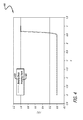
- FIG. 4 is a graph 400 showing the current-voltage (I-V) curve of the disclosed diode of FIG. 2B with improved metal contacts verses (vs.) an existing diode.
- test data is graphed to show a comparison of the I-V curve 420 for the disclosed diode with improved metal contacts verses the I-V curve 410 for an existing diode without SiO 2 protection (i.e. without a protective dielectric layer).
- the I-V characteristics of the disclosed diode with improved metal contacts are equivalent to the I-V characteristics for an existing diode without SiO 2 protection.
Landscapes
- Electrodes Of Semiconductors (AREA)
- Engineering & Computer Science (AREA)
- Photovoltaic Devices (AREA)
- Life Sciences & Earth Sciences (AREA)
- Sustainable Development (AREA)
- Sustainable Energy (AREA)
- Manufacturing & Machinery (AREA)
Abstract
Description
- The present disclosure relates to by-pass diodes. In particular, it relates to solar cell by-pass diodes with improved metal contacts.
- Titanium is typically used for the ohmic contacts of silicon diodes by forming titanium silicide. However, oxygen in the environment oxidizes titanium during the metal contact sinter process, which is typically run in a temperature range from 300 degrees Celsius to 600 degrees Celsius. The oxidized titanium layer weakens metal contact adhesion to silicon and, as such, the reliability of the diodes is compromised.
- Therefore, a solar cell by-pass diode with improved metal contacts is needed.
- The present disclosure relates to a method, system, and apparatus for a solar cell by-pass diode with improved metal contacts. The disclosed method for manufacturing a solar cell by-pass diode involves forming a first doping layer, by diffusion or ion implant, on a first side of a silicon wafer. The method further involves depositing by chemical vapor deposition (CVD) a first dielectric layer (e.g., a SiO2 layer) on the first doping layer and on a second side of the silicon wafer. Also, the method involves etching an opening in the first dielectric layer on the second side of the silicon wafer. In addition, the method involves performing diffusion or ion implant over the opening to create a junction. Additionally, the method involves removing the first dielectric layer from the first doping layer and from the second side of the silicon wafer. Also, the method involves depositing a first metal contact on the junction, and depositing a second metal contact on the first doping layer. In addition, the method involves depositing by CVD a second dielectric layer (e.g., a SiO2 layer) on the first metal contact, on an exposed portion of the second side of the silicon wafer, and on the second metal contact. Further, the method involves etching an opening in the second dielectric layer on the first metal contact.
- In one or more embodiments, the method further involves, after forming the first doping layer on the first side of a silicon wafer, depositing by CVD an initial dielectric layer (e.g., a SiO2 layer) on the first doping layer and on the second side of the silicon wafer. In at least one embodiment, the method further involves performing thermal annealing. In some embodiments, the method further involves removing the initial dielectric layer from the first doping layer and from the second side of the silicon wafer.
- In at least one embodiment, the removing of the initial dielectric layer from the first doping layer and from the second side of the silicon wafer is performed by using hydrofluoric acid. In some embodiments, the method further involves, prior to etching the opening in the second dielectric layer on the first metal contact, sintering the first metal contact and the second metal contact.
- In one or more embodiments, the first doping layer is a p-type material. In at least one embodiment, the p-type material of the first doping layer is boron (B).
- In some embodiments, the first metal contact is a titanium, palladium, and silver (Ti/Pd/Ag) alloy; or is an aluminum, titanium, palladium, and silver (Al/Ti/Pd/Ag) alloy. In one or more embodiments, the second metal contact is a titanium, palladium, and silver (Ti/Pd/Ag) alloy; or is an aluminum, titanium, palladium, and silver (Al/Ti/Pd/Ag) alloy.
- In at least one embodiment, the first dielectric layer is silicon dioxide (SiO2). In one or more embodiments, the second dielectric layer is silicon dioxide (SiO2). In some embodiments, the initial dielectric layer is silicon dioxide (SiO2).
- In at least one embodiment, the first doping layer is an n-type material. In some embodiments, the n-type material of the first doping layer is phosphorous (P).
- In one or more embodiments, the etching of the opening in the first dielectric layer on the second side of the silicon wafer is performed by using at least one of photolithography and hydrofluoric acid. In at least one embodiment, the removing of the first dielectric layer from the first doping layer and from the second side of the silicon wafer is performed by using hydrofluoric acid. In some embodiments, the depositing of the first metal contact on the junction and the depositing of the second metal contact on the first doping layer are performed by using electron-beam (e-beam) evaporation.
- In at least one embodiment, a method for manufacturing a solar cell by-pass diode is disclosed. The disclosed method involves depositing a first dielectric layer on a first side of a silicon wafer. The method further involves etching a first opening in the first dielectric layer. Also, the method involves forming a first doping layer, by performing diffusion or ion implant, over the first opening to create a junction. In addition, the method involves depositing a second dielectric layer over the first doping layer and exposed silicon area of the first side. Also, the method involves etching a second opening in the second dielectric layer, where the second opening is at a different location than the first opening. In addition, the method involves forming a second doping layer, by diffusion or ion implant, over the second opening. Additionally, the method involves removing the second dielectric layer on top of the first doping layer. In addition, the method involves depositing a metal contact on the first doping layer forming a first metal contact, and depositing a metal contact on the second doping layer forming a second metal contact. Additionally, the method involves depositing a third dielectric layer on the first metal contact and on the second metal contact. Further, the method involves etching two openings in the third dielectric layer over the first metal contact and over the second metal contact.
- In one or more embodiments embodiments, the method further involves, prior to etching the opening in the third dielectric layer on top of the first metal contact and the second metal contact, sintering the two metal contacts.
- In at least one embodiment, the first doping layer is a p-type material, and the second doping layer is an n-type material. In one or more embodiments, the p-type material of the first doping layer is boron (B), and the n-type material of the second doping layer is phosphorus (P).
- In one or more embodiments, the first doping layer is an n-type material, and the second doping layer is a p-type material. In some embodiments, the first metal contact is a titanium, palladium, and silver (Al/Ti/Pd/Ag) alloy or an aluminum, titanium, palladium, and silver (Al/Ti/Pd/Ag) alloy. In one or more embodiments, the second metal contact is a titanium, palladium, and silver (Al/Ti/Pd/Ag) alloy or an aluminum, titanium, palladium, and silver (Al/Ti/Pd/Ag) alloy.
- In at least one embodiment, the first dielectric layer and/or the second dielectric layer and/or the third dielectric layer is silicon dioxide (SiO2). In some embodiments, the etching of the opening in the first dielectric layer, in the second dielectric layer, and/or in the third dielectric layer on the silicon wafer is performed by using photolithography and/or hydrofluoric acid. In one or more embodiments, the depositing of the first metal contact on the junction, and the depositing of the second metal contact on the second doping layer are performed by using electron-beam evaporation.
- In at least one embodiment, a solar cell by-pass diode comprises a silicon wafer, and a
type 2 doping layer formed on a first side of the silicon wafer. The solar cell by-pass diode further comprises atype 1 doping layer diffused or implanted into a portion of a second side of the silicon wafer. Also, the solar cell by-pass diode comprises a front metal contact deposited on thetype 1 doping layer. In addition, the solar cell by-pass diode comprises a back metal contact deposited on thetype 2 doping layer. Further, the solar cell by-pass diode comprises a dielectric layer deposited on the front metal contact and an exposed portion of the second side of the silicon wafer, where the dielectric layer has an opening exposing the front metal contact. - In one or more embodiments, the
type 2 doping layer is an n-type material. In some embodiments, thetype 2 doping layer is a p-type material. - In at least one embodiment, a solar cell by-pass diode comprises a silicon wafer. The diode further comprises a type1 doping layer formed on a first portion of a first side of the silicon wafer, and a
type 2 doping layer formed on a second portion of the first side of the silicon wafer. In addition, the diode comprises atype 1 metal contact deposited on thetype 1 doping layer, and atype 2 metal contact deposited on thetype 2 doping layer. Additionally, the diode comprises a dielectric layer deposited on thetype 1 metal contact and thetype 2 metal contact, and on an exposed portion of the silicon wafer, where the dielectric layer has two openings exposing thetype 1 metal contact and thetype 2 metal contact. - In one or more embodiments, the
type 2 doping layer is an n-type material, and thetype 1 doping layer is a p-type material. In some embodiments, thetype 2 doping layer is a p-type material, and thetype 1 doping layer is an n-type material. - The features, functions, and advantages can be achieved independently in various embodiments of the present inventions or may be combined in yet other embodiments.
- These and other features, aspects, and advantages of the present disclosure will become better understood with regard to the following description, appended claims, and accompanying drawings where:
-
FIG. 1 is a graph showing the diode metal contact weld-pull strength and percentage peeling versus (vs.) the oxygen level in the metal contact of an existing diode. -
FIG. 2A is a cross-sectional view of an existing diode structure. -
FIG. 2B is a cross-sectional view of the diode structure for the disclosed diode with improved metal contacts, in accordance with at least one embodiment of the present disclosure. -
FIG. 2C is a cross-sectional view of another diode structure for the disclosed diode with improved metal contacts, in accordance with at least one embodiment of the present disclosure. -
FIGS. 3A and3B depict the steps of the disclosed method for fabrication of the diode with improved metal contacts ofFIG. 2B , in accordance with at least one embodiment of the present disclosure. -
FIG. 4 is a graph showing the current-voltage (I-V) curve of the disclosed diode with improved metal contacts ofFIG. 2B verses (vs.) an existing diode. - The methods and apparatus disclosed herein provide an operative system for a solar cell by-pass diode with improved metal contacts. Specifically, the system improves solar cell by-pass diode metal contact adhesion by employing a dielectric film on top of the metal contact during the metal contact sintering process. The dielectric film prevents the contact metal from becoming oxidized during the sintering, and also prevents a short circuit in the diode and the solar cell assembly.
- As previously mentioned above, titanium (Ti) is typically used for the ohmic contacts of silicon (Si) diodes by forming titanium silicide (TiSi2). But, oxygen (O2) in the environment oxidizes the titanium during the metal contact sinter process. The oxidized titanium layer weakens metal contact adhesion to silicon and, thus, such diodes cannot be used for space applications.
- Currently, in industry, to prevent titanium oxidation of the metal contacts during the metal sinter process, the metal sinter process is performed in a furnace tube with inert gasses, such as nitrogen (N2) or N2 with a low content of hydrogen (H2), purged into the furnace tube. However, even with employing the above-mentioned metal sinter process, oxygen in the air can diffuse into the furnace tube through its open exhaust and react with the titanium. The extent of titanium oxidation depends upon the location of the wafer in the furnace during the sintering process. Wafers located close to the exhaust of the furnace tube oxidize more than wafers located further away from the exhaust. Other than using a sinter process in a controlled environment, such as in a furnace tube, a variety of different types of contact stacks have been investigated for oxygen resilience, such as employing a palladium metal on top of the titanium to serve as an oxygen barrier. However, even with using any of these conventional solutions, metal oxidation still exists to an extent that detrimentally affects the yielded product.
- The system of the present disclosure employs a dielectric layer, such as a chemical vapor deposition (CVD) silicon dioxide (SiO2) layer, to cover the metal contacts of the diode during the metal sintering process, thereby preventing the titanium layer of the metal contacts from becoming oxidized. The atomic percentage of oxygen in the metal contacts of diodes with SiO2 protection, detected with energy-dispersive x-ray spectroscopy (EDX), is one tenth of that in the metal contacts of diodes without SiO2 protection.
- In the following description, numerous details are set forth in order to provide a more thorough description of the system. It will be apparent, however, to one skilled in the art, that the disclosed system may be practiced without these specific details. In the other instances, well known features have not been described in detail so as not to unnecessarily obscure the system.
-
FIG. 1 is agraph 100 showing the diode metal contact weld-pull strength and percentage peeling versus (vs.) the oxygen level in the metal contact of an existing diode. In this figure, silicon diode metal contact adhesion, of a contact manufactured from a titanium, palladium, and silver (Ti/Pd/Ag) alloy, versus the oxygen content detected by energy-dispersive x-ray spectroscopy (EDX) is demonstrated through a weld pull test. As is shown in this figure, as the oxygen (O2) content increases, the weld pull strength in grams (g) decreases and the percentage of peeling on the weld footprint increases. - The diode of the present disclosure employs a dielectric film to cover the metal contacts during the sinter process. The dielectric film cover causes the metal contacts to have little exposure to oxygen, which oxidizes the titanium in the contacts. Since the dielectric film cover causes the metal contacts to have little exposure to oxygen, the metal contacts exhibit less oxidation and, thus, the metal contact adhesion is improved.
-
FIG. 2A is a cross-sectional view of an existingdiode structure 200. In this figure, atype 2doping layer 210 is shown to be formed, by diffusion or ion implant, on afirst side 207 of asilicon wafer 215. In addition, atype 1doping layer 220 is shown to be diffused (or implanted) into a portion of asecond side 217 of thesilicon wafer 215. - Also in this figure, a
dielectric layer 225 is shown to be in two areas on top of thesecond side 217 of thesilicon wafer 215. Afront metal contact 235 is shown to be deposited on thetype 1doping layer 220, and aback metal contact 205 is shown to be deposited on thetype 2doping layer 210. In addition, apassivation layer 230 is shown to be on top of thedielectric layer 225 areas. - For this existing
diode structure 200, thefront metal contact 235 is sintered before being passivated. Thepassivation layer 230 is for preventing a short circuit in thediode 200 and the solar cell assembly (not shown). -
FIG. 2B is a cross-sectional view of thediode structure 240 for the disclosed diode with improved metal contacts, in accordance with at least one embodiment of the present disclosure. In this figure, atype 2doping layer 250 is shown to be formed, by diffusion or by ion implant, on afirst side 247 of asilicon wafer 255. In addition, atype 1doping layer 260 is shown to be diffused or ion implanted into a portion of asecond side 257 of thesilicon wafer 255. - Also in this figure, a
front metal contact 270 is shown to be deposited on thetype 1doping layer 260, and aback metal contact 245 is shown to be deposited on thetype 2doping layer 250. In addition, a dielectric layer 265 (e.g., SiO2 material) is shown to be in two areas on top of thesecond side 257 of thesilicon wafer 255. - For this disclosed
diode structure 240, thefront metal contact 270 is covered with a dielectric film 265 before it is sintered so that the metal layers in thefront metal contact 270 are isolated from oxygen in the environment. The dielectric layer 265 is partially removed in the end of the process to expose thefront metal contact 270. - It should be noted that in one or more embodiments, the
type 2doping layer 250 is an n-type material (e.g., phosphorous (P)), thesilicon wafer 255 is an n-type material, andtype 1doping layer 260 is a p-type material (e.g., boron (B)). In other embodiments, thetype 2doping layer 250 is a p-type material (e.g., boron (B)), thesilicon wafer 255 is a p-type material, andtype 1doping layer 260 is an n-type material (e.g., phosphorous (P)). -
FIG. 2C is a cross-sectional view of anotherdiode structure 280 for the disclosed diode with improved metal contacts, in accordance with at least one embodiment of the present disclosure. In this figure, atype 1doping layer 282 is shown to be formed, by diffusion or by ion implant, on a first portion of afirst side 281 of asilicon wafer 286. In addition, atype 2doping layer 284 is shown to be formed, by diffusion or ion implant, on a second portion of thefirst side 281 of thesilicon wafer 286. - Also in this figure, a
first metal contact 290 is shown to be deposited on thetype 1doping layer 282, and asecond metal contact 292 is shown to be deposited on thetype 2doping layer 284. In addition, a dielectric layer 288 (e.g., a SiO2 material) is shown to be located in the three areas on top of thesilicon wafer 286. - For this disclosed
diode structure 280, thefirst metal contact 290 and thesecond metal contact 292 are both covered with adielectric film 288 before thediode 280 is sintered so that themetal contacts dielectric layer 288 is partially removed at the end of the process to expose themetal contacts - It should be noted that in one or more embodiments, the
type 1doping layer 282 is an n-type material (e.g., phosphorous (P)), thesilicon wafer 286 is a p-type material, andtype 2doping layer 284 is a p-type material (e.g., boron (B)). In other embodiments, thetype 1doping layer 282 is a p-type material (e.g., boron (B)), thesilicon wafer 286 is an n-type material, andtype 2doping layer 284 is an n-type material (e.g., phosphorous (P)). -
FIGS. 3A and3B depict the steps of the disclosed method for fabrication of the diode with improved metal contacts ofFIG. 2B , in accordance with at least one embodiment of the present disclosure. In these figures, in particular, the steps for the method for manufacturing the diode ofFIG. 2 from a p-type silicon wafer are depicted. It should be noted that, in other embodiments, with this method the diode may be manufactured from an n-type silicon wafer as well. - Turning to
FIG. 3A , step (a) depicts a heavy p-typefirst doping layer 305 being formed (i.e. implanted or diffused) on a first side (i.e. the backside) 307 of the p-type silicon wafer 300 by, for example, a Boron implant or a diffusion process. Step (b) illustrates an optional initial SiO2 layer (i.e. a dielectric layer) 310, 315 being deposited by chemical vapor deposition (CVD) on thefirst doping layer 305 and on thesecond side 317 of thesilicon wafer 300; and thermal annealing performed afterward for alleviating crystal damage from the implantation process. It should be noted that step (b) does not need to be performed if the heavy p-type doping of thefirst doping layer 305 in step (a) is formed by a diffusion process, rather than by an implantation process. - Step (c) shows that the initial SiO2 layer 310, 315 is removed (i.e. etched off) by soaking the
silicon wafer 300 in hydrofluoric acid. Step (d) illustrates a first SiO2 layer (i.e. a dielectric layer) 320, 325 being deposited by chemical vapor deposition (CVD) on thefirst doping layer 305 and on thesecond side 317 of thesilicon wafer 300, where the SiO2 layer (i.e. dielectric layer) 320, 325 is to be a diffusion mask. Step (e) shows that through photolithography and/or hydrofluoric acid etching, anopening 330 is formed in the first SiO2 layer 325 (i.e. the first SiO2 layer 325 is patterned to have an opening 330) to be a diffusion window. Step (f) depicts ap-n junction 335 created by phosphor diffusion that is performed in a furnace (not shown). - Turning to
FIG. 3B , step (g) shows that the first SiO2 layer 320, 325 is removed (i.e. etched off) by soaking thesilicon wafer 300 in hydrofluoric acid. Step (h) illustrates a first metal contact (i.e. a front metal contact) 340 (e.g., an n-contact metal, such as a Ti/Pd/Ag alloy) being deposited by electron-beam (e-beam) evaporation. Step (i) shows a second metal contact (i.e. a back metal contact) 345 (e.g., a p-contact metal, such as a Ti/Pd/Ag alloy) being deposited by electron-beam (e-beam) evaporation. - Step (j) depicts a second SiO2 layer (i.e. a dielectric layer) 350, 355 being deposited by chemical vapor deposition (CVD) on the
first metal contact 340, on an exposed portion of thesecond side 317 of thesilicon wafer 300, and on thesecond metal contact 345. It should be noted that the second SiO2 layer 350, 355 may be manufactured from other materials other than SiO2, such as silicon nitride (Si3N4). In addition, in other embodiments, other techniques other than CVD may be employed to deposit the second SiO2 layer 350, 355. Other techniques that may be used include, but are not limited to, low pressure chemical vapor deposition (LPCVD) and plasma enhanced chemical vapor deposition (PECVD). - Step (k) shows that, optionally, the
first metal contact 340 and thesecond metal contact 345 are sintered. It should be noted that sintering is not needed if the CVD process in step (j) is performed for a similar time duration and similar temperature as is required for ohmic contact sintering. Step (I) shows that through hydrofluoric acid etching, anopening 360 is formed in the second SiO2 layer 355. Step (I) also shows the second SiO2 layer 350 is removed (i.e. etched off) by hydrofluoric acid. The remaining portion of the second SiO2 layer 355 is left to passivate thep-n junction 335 and to prevent a short circuit in the diode and solar cell assembly. -
FIG. 4 is agraph 400 showing the current-voltage (I-V) curve of the disclosed diode ofFIG. 2B with improved metal contacts verses (vs.) an existing diode. In this figure, test data is graphed to show a comparison of the I-V curve 420 for the disclosed diode with improved metal contacts verses theI-V curve 410 for an existing diode without SiO2 protection (i.e. without a protective dielectric layer). As is depicted in the figure, the I-V characteristics of the disclosed diode with improved metal contacts are equivalent to the I-V characteristics for an existing diode without SiO2 protection. - The following items are disclosed:
-
Item 1. A method for manufacturing a solar cell by-pass diode, the method comprising:- forming a first doping layer on a first side of a silicon wafer;
- depositing a first dielectric layer on the first doping layer and on a second side of the silicon wafer;
- etching an opening in the first dielectric layer on the second side of the silicon wafer;
- performing one of diffusion and ion implant over the opening to create a junction;
- removing the first dielectric layer from the first doping layer and from the second side of the silicon wafer;
- depositing a first metal contact on the junction, and depositing a second metal contact on the first doping layer; depositing a second dielectric layer on the first metal contact, on an exposed portion of the second side of the silicon wafer, and on the second metal contact; and
- etching an opening in the second dielectric layer on the first metal contact; and
- removing the second dielectric layer on the second metal contact.
-
Item 2. The method ofitem 1, wherein the method further comprises, after forming the first doping layer on the first side of a silicon wafer, depositing an initial dielectric layer on the first doping layer and on the second side of the silicon wafer. -
Item 3. The method ofitem 2, wherein the method further comprises performing thermal annealing. -
Item 4. The method ofitem 3, wherein the method further comprises removing the initial dielectric layer from the first doping layer and from the second side of the silicon wafer. - Item 5. The method of
item 4, wherein the removing of the initial dielectric layer from the first doping layer and from the second side of the silicon wafer is performed by using hydrofluoric acid. -
Item 6. The method ofitem 1, wherein the method further comprises, prior to etching the opening in the second dielectric layer on the first metal contact, sintering the first metal contact and the second metal contact. - Item 7. The method of
item 1, wherein the first doping layer is a p-type material. -
Item 8. The method of item 7, wherein the p-type material of the first doping layer is boron (B). - Item 9. The method of
item 1, wherein the first metal contact is one of a titanium, palladium, and silver (Ti/Pd/Ag) alloy; and an aluminum, titanium, palladium, and silver (Al/Ti/Pd/Ag) alloy. -
Item 10. The method ofitem 1, wherein the second metal contact is one of a titanium, palladium, and silver (Ti/Pd/Ag) alloy; and an aluminum, titanium, palladium, and silver (Al/Ti/Pd/Ag) alloy. - Item 11. The method of
item 1, wherein the first doping layer is an n-type material. -
Item 12. The method of item 11, wherein the n-type material of the first doping layer is phosphorous (P). - Item 13. The method of
item 1, wherein at least one of the first dielectric layer and the second dielectric layer is silicon dioxide (SiO2). - Item 14. The method of
item 1, wherein the etching of the opening in the first dielectric layer on the second side of the silicon wafer is performed by using at least one of photolithography and hydrofluoric acid. - Item 15. The method of
item 1, wherein the removing of the first dielectric layer from the first doping layer and from the second side of the silicon wafer is performed by using hydrofluoric acid. - Item 16. The method of
item 1, wherein the depositing of the first metal contact on the junction and the depositing of the second metal contact on the first doping layer are performed by using electron-beam evaporation. - Item 17. A method for manufacturing a solar cell by-pass diode, the method comprising:
- depositing a first dielectric layer on a first side of a silicon wafer;
- etching a first opening in the first dielectric layer;
- forming a first doping layer over the first opening to create a junction;
- depositing a second dielectric layer over the first doping layer and exposed silicon area of the first side;
- etching a second opening in the second dielectric layer;
- forming a second doping layer over the second opening;
- removing the second dielectric layer on top of the first doping layer;
- depositing a metal contact on the first doping layer forming a first metal contact and on the second doping layer forming a second metal contact;
- depositing a third dielectric layer on the first metal contract and on the second metal contact;
- etching two openings in the third dielectric layer over the first metal contact and over the second metal contact.
- Item 18. A solar cell by-pass diode, the diode comprising:
- a silicon wafer;
- a
type 2 doping layer formed on a first side of the silicon wafer; - a
type 1 doping layer that is one of diffused and implanted into a portion of a second side of the silicon wafer; - a front metal contact deposited on the
type 1 doping layer; - a back metal contact deposited on the
type 2 doping layer; and - a dielectric layer deposited on the front metal contact and an exposed portion of the second side of the silicon wafer, wherein the dielectric layer has an opening exposing the front metal contact.
- Item 19. The diode of item 18, wherein the
type 2 doping layer is an n-type material. -
Item 20. The diode of item 18, wherein thetype 2 doping layer is a p-type material. - Item 21. A solar cell by-pass diode, the diode comprising:
- a silicon wafer;
- a type1 doping layer formed on a first portion of a first side of the silicon wafer;
- a
type 2 doping layer formed on a second portion of the first side of the silicon wafer; - a
type 1 metal contact deposited on thetype 1 doping layer; - a
type 2 metal contact deposited on thetype 2 doping layer; - a dielectric layer deposited on the
type 1 metal contact and thetype 2 metal contact, and on an exposed portion of the silicon wafer, wherein the dielectric layer has two openings exposing thetype 1 metal contact and thetype 2 metal contact.
- Although certain illustrative embodiments and methods have been disclosed herein, it can be apparent from the foregoing disclosure to those skilled in the art that variations and modifications of such embodiments and methods can be made without departing from the scope of the disclosure. Many other examples of the disclosure exist, each differing from others in matters of detail only. Accordingly, it is intended that the disclsoure shall be limited only to the extent required by the appended claims and the rules and principles of applicable law.
Claims (15)
- A method for manufacturing a solar cell by-pass diode, the method comprising:forming a first doping layer on a first side of a silicon wafer;depositing a first dielectric layer on the first doping layer and on a second side of the silicon wafer;etching an opening in the first dielectric layer on the second side of the silicon wafer;performing one of diffusion and ion implant over the opening to create a junction;removing the first dielectric layer from the first doping layer and from the second side of the silicon wafer;depositing a first metal contact on the junction, and depositing a second metal contact on the first doping layer;depositing a second dielectric layer on the first metal contact, on an exposed portion of the second side of the silicon wafer, and on the second metal contact; andetching an opening in the second dielectric layer on the first metal contact; andremoving the second dielectric layer on the second metal contact.
- The method of claim 1, wherein the method further comprises, after
forming
the first doping layer on the first side of a silicon wafer, depositing an initial dielectric layer on the first doping layer and on the second side of the silicon wafer. - The method of claim 1 or 2, wherein the method further comprises
performing
thermal annealing. - The method of any of claims 1-3, wherein the method further comprises
removing the
initial dielectric layer from the first doping layer and from the second side of the silicon wafer. - The method of any of claims 1-4, wherein the removing of the initial
dielectric layer from
the first doping layer and from the second side of the silicon wafer is performed by using hydrofluoric acid. - The method of any preceding claim, wherein the method further
comprises, prior to etching
the opening in the second dielectric layer on the first metal contact, sintering the first metal contact and the second metal contact. - The method of any preceding claim, wherein the first doping layer is a p-type material.
- The method of any preceding claim, wherein the first metal contact is one
of a titanium,
palladium, and silver (Ti/Pd/Ag) alloy; and an aluminum, titanium, palladium, and silver (Al/Ti/Pd/Ag) alloy. - The method of any preceding claim, wherein the second metal contact is
one of a titanium,
palladium, and silver (Ti/Pd/Ag) alloy; and an aluminum, titanium, palladium, and silver (Al/Ti/Pd/Ag) alloy. - The method of any preceding claim, wherein the first doping layer is an n-type material.
- The method of any preceding claim, wherein at least one of the first
dielectric layer and the
second dielectric layer is silicon dioxide (SiO2). - The method of any preceding claim, wherein the etching of the opening in
the first
dielectric layer on the second side of the silicon wafer is performed by using at least one of photolithography and hydrofluoric acid. - The method of any preceding claim, wherein the removing of the first
dielectric layer from
the first doping layer and from the second side of the silicon wafer is performed by using hydrofluoric acid. - The method of any preceding claim, wherein the depositing of the first
metal contact on the
junction and the depositing of the second metal contact on the first doping layer are performed by using electron-beam evaporation. - A solar cell by-pass diode, the diode comprising:a silicon wafer;a type 2 doping layer formed on a first side of the silicon wafer;a type 1 doping layer that is one of diffused and implanted into a portion of a second side of the silicon wafer;a front metal contact deposited on the type 1 doping layer;a back metal contact deposited on the type 2 doping layer; anda dielectric layer deposited on the front metal contact and an exposed portion of the second side of the silicon wafer, wherein the dielectric layer has an opening exposing the front metal contact.
Applications Claiming Priority (1)
| Application Number | Priority Date | Filing Date | Title |
|---|---|---|---|
| US13/874,981 US9147779B2 (en) | 2013-05-01 | 2013-05-01 | Solar cell by-pass diode with improved metal contacts |
Publications (2)
| Publication Number | Publication Date |
|---|---|
| EP2800126A1 true EP2800126A1 (en) | 2014-11-05 |
| EP2800126B1 EP2800126B1 (en) | 2020-02-19 |
Family
ID=50231043
Family Applications (1)
| Application Number | Title | Priority Date | Filing Date |
|---|---|---|---|
| EP14158253.6A Active EP2800126B1 (en) | 2013-05-01 | 2014-03-07 | Diode with improved metal contacts and its manufacturing method |
Country Status (3)
| Country | Link |
|---|---|
| US (1) | US9147779B2 (en) |
| EP (1) | EP2800126B1 (en) |
| JP (1) | JP5936646B2 (en) |
Cited By (1)
| Publication number | Priority date | Publication date | Assignee | Title |
|---|---|---|---|---|
| CN106026905A (en) * | 2016-06-24 | 2016-10-12 | 常州天合光能有限公司 | Photovoltaic assembly with built-in diodes |
Families Citing this family (1)
| Publication number | Priority date | Publication date | Assignee | Title |
|---|---|---|---|---|
| US10744563B2 (en) | 2016-10-17 | 2020-08-18 | The Boeing Company | 3D printing of an object from powdered material using pressure waves |
Citations (5)
| Publication number | Priority date | Publication date | Assignee | Title |
|---|---|---|---|---|
| JPS58213469A (en) * | 1982-06-07 | 1983-12-12 | Hitachi Ltd | Contact electrode and manufacture thereof |
| EP0211174A2 (en) * | 1985-08-06 | 1987-02-25 | Motorola, Inc. | Monolithic temperature compensated voltage-reference diode and method for its manufacture |
| US4690730A (en) * | 1986-03-07 | 1987-09-01 | Texas Instruments Incorporated | Oxide-capped titanium silicide formation |
| JP2005020021A (en) * | 2004-08-26 | 2005-01-20 | Toshiba Corp | Manufacturing method of semiconductor element and W material for magnetron sputtering apparatus |
| US20060214184A1 (en) * | 2005-03-25 | 2006-09-28 | Benson Wang | Process for forming a planar diode using one mask |
Family Cites Families (16)
| Publication number | Priority date | Publication date | Assignee | Title |
|---|---|---|---|---|
| US3903427A (en) * | 1973-12-28 | 1975-09-02 | Hughes Aircraft Co | Solar cell connections |
| JPS60182133A (en) * | 1984-02-29 | 1985-09-17 | Fujitsu Ltd | Manufacture of semiconductor device |
| JPS61168266A (en) * | 1985-01-21 | 1986-07-29 | Toshiba Corp | Manufacture of mis type semiconductor device |
| US4838952A (en) * | 1988-04-29 | 1989-06-13 | Spectrolab, Inc. | Controlled reflectance solar cell |
| JPH04276665A (en) * | 1991-03-04 | 1992-10-01 | Canon Inc | integrated solar cells |
| JP2755281B2 (en) * | 1992-12-28 | 1998-05-20 | 富士電機株式会社 | Thin film solar cell and method of manufacturing the same |
| US5468988A (en) * | 1994-03-04 | 1995-11-21 | United Solar Systems Corporation | Large area, through-hole, parallel-connected photovoltaic device |
| EP0881694A1 (en) * | 1997-05-30 | 1998-12-02 | Interuniversitair Micro-Elektronica Centrum Vzw | Solar cell and process of manufacturing the same |
| US6635507B1 (en) * | 1999-07-14 | 2003-10-21 | Hughes Electronics Corporation | Monolithic bypass-diode and solar-cell string assembly |
| JP2003142579A (en) * | 2001-11-07 | 2003-05-16 | Hitachi Ltd | Semiconductor device manufacturing method and semiconductor device |
| US7656001B2 (en) * | 2006-11-01 | 2010-02-02 | Udt Sensors, Inc. | Front-side illuminated, back-side contact double-sided PN-junction photodiode arrays |
| US7144751B2 (en) * | 2004-02-05 | 2006-12-05 | Advent Solar, Inc. | Back-contact solar cells and methods for fabrication |
| US20060060238A1 (en) * | 2004-02-05 | 2006-03-23 | Advent Solar, Inc. | Process and fabrication methods for emitter wrap through back contact solar cells |
| KR101212198B1 (en) * | 2006-04-06 | 2012-12-13 | 삼성에스디아이 주식회사 | Solar cell |
| JP2008294080A (en) * | 2007-05-22 | 2008-12-04 | Sanyo Electric Co Ltd | Solar cell and method for manufacturing solar cell |
| US8115097B2 (en) * | 2009-11-19 | 2012-02-14 | International Business Machines Corporation | Grid-line-free contact for a photovoltaic cell |
-
2013
- 2013-05-01 US US13/874,981 patent/US9147779B2/en not_active Expired - Fee Related
-
2014
- 2014-03-07 EP EP14158253.6A patent/EP2800126B1/en active Active
- 2014-04-25 JP JP2014091000A patent/JP5936646B2/en not_active Expired - Fee Related
Patent Citations (5)
| Publication number | Priority date | Publication date | Assignee | Title |
|---|---|---|---|---|
| JPS58213469A (en) * | 1982-06-07 | 1983-12-12 | Hitachi Ltd | Contact electrode and manufacture thereof |
| EP0211174A2 (en) * | 1985-08-06 | 1987-02-25 | Motorola, Inc. | Monolithic temperature compensated voltage-reference diode and method for its manufacture |
| US4690730A (en) * | 1986-03-07 | 1987-09-01 | Texas Instruments Incorporated | Oxide-capped titanium silicide formation |
| JP2005020021A (en) * | 2004-08-26 | 2005-01-20 | Toshiba Corp | Manufacturing method of semiconductor element and W material for magnetron sputtering apparatus |
| US20060214184A1 (en) * | 2005-03-25 | 2006-09-28 | Benson Wang | Process for forming a planar diode using one mask |
Cited By (2)
| Publication number | Priority date | Publication date | Assignee | Title |
|---|---|---|---|---|
| CN106026905A (en) * | 2016-06-24 | 2016-10-12 | 常州天合光能有限公司 | Photovoltaic assembly with built-in diodes |
| CN106026905B (en) * | 2016-06-24 | 2018-01-09 | 常州天合光能有限公司 | A kind of photovoltaic module of diode-built-in |
Also Published As
| Publication number | Publication date |
|---|---|
| EP2800126B1 (en) | 2020-02-19 |
| JP5936646B2 (en) | 2016-06-22 |
| JP2014220497A (en) | 2014-11-20 |
| US20140326304A1 (en) | 2014-11-06 |
| US9147779B2 (en) | 2015-09-29 |
Similar Documents
| Publication | Publication Date | Title |
|---|---|---|
| US6800543B2 (en) | Semiconductor device having a low-resistance gate electrode | |
| US8865591B2 (en) | N-type contact electrode formed on an N-type semiconductor layer and method of forming same using a second metal electrode layer heat-treated after being formed on a first, heat-treated metal electrode layer | |
| US9142696B2 (en) | Solar cells with silicon nanoparticles that are coated with nanoparticle passivation film | |
| JP2014512673A (en) | Efficient black silicon photovoltaic device with improved blue sensitivity | |
| JPH10200161A (en) | Contact electrode of n-type gallium nitride based semiconductor and method of forming the same | |
| US20100186803A1 (en) | Buried insulator isolation for solar cell contacts | |
| US4105471A (en) | Solar cell with improved printed contact and method of making the same | |
| WO2009094575A2 (en) | Buried insulator isolation for solar cell contacts | |
| CN104241443A (en) | Solar cell and manufacturing method thereof | |
| JP4191000B2 (en) | Semiconductor device and manufacturing method thereof | |
| US20200295220A1 (en) | Method for Fabrication of Germanium Photodiode with Silicon Cap | |
| US9147779B2 (en) | Solar cell by-pass diode with improved metal contacts | |
| JP5593619B2 (en) | Schottky barrier diode and manufacturing method thereof | |
| WO2011160819A2 (en) | Method for fabrication of a back side contact solar cell | |
| US20070173045A1 (en) | Method of manufacturing semiconductor device | |
| EP0209196A2 (en) | Method of controlling forward voltage across schottky diode | |
| US20020001945A1 (en) | Method of manufacturing metal pattern of semiconductor device | |
| JP2003017749A (en) | Metal electrode for light emitting diode using n-type zinc oxide based semiconductor and method of manufacturing the same | |
| JP6733588B2 (en) | Method of manufacturing semiconductor device | |
| JPH03289156A (en) | Semiconductor device and its manufacturing method | |
| JP2003209067A (en) | Semiconductor device and method for forming electrical connection of semiconductor device | |
| JP2008060161A (en) | Photodetector and method for manufacturing the same | |
| JP2005159171A (en) | Solar cell element and manufacturing method thereof | |
| US20140000693A1 (en) | Integration of a titania layer in an anti-reflective coating | |
| JP3341329B2 (en) | Method for manufacturing semiconductor device |
Legal Events
| Date | Code | Title | Description |
|---|---|---|---|
| PUAI | Public reference made under article 153(3) epc to a published international application that has entered the european phase |
Free format text: ORIGINAL CODE: 0009012 |
|
| 17P | Request for examination filed |
Effective date: 20140307 |
|
| AK | Designated contracting states |
Kind code of ref document: A1 Designated state(s): AL AT BE BG CH CY CZ DE DK EE ES FI FR GB GR HR HU IE IS IT LI LT LU LV MC MK MT NL NO PL PT RO RS SE SI SK SM TR |
|
| AX | Request for extension of the european patent |
Extension state: BA ME |
|
| STAA | Information on the status of an ep patent application or granted ep patent |
Free format text: STATUS: EXAMINATION IS IN PROGRESS |
|
| 17Q | First examination report despatched |
Effective date: 20171206 |
|
| GRAP | Despatch of communication of intention to grant a patent |
Free format text: ORIGINAL CODE: EPIDOSNIGR1 |
|
| STAA | Information on the status of an ep patent application or granted ep patent |
Free format text: STATUS: GRANT OF PATENT IS INTENDED |
|
| INTG | Intention to grant announced |
Effective date: 20190806 |
|
| GRAS | Grant fee paid |
Free format text: ORIGINAL CODE: EPIDOSNIGR3 |
|
| GRAJ | Information related to disapproval of communication of intention to grant by the applicant or resumption of examination proceedings by the epo deleted |
Free format text: ORIGINAL CODE: EPIDOSDIGR1 |
|
| GRAL | Information related to payment of fee for publishing/printing deleted |
Free format text: ORIGINAL CODE: EPIDOSDIGR3 |
|
| STAA | Information on the status of an ep patent application or granted ep patent |
Free format text: STATUS: EXAMINATION IS IN PROGRESS |
|
| GRAJ | Information related to disapproval of communication of intention to grant by the applicant or resumption of examination proceedings by the epo deleted |
Free format text: ORIGINAL CODE: EPIDOSDIGR1 |
|
| GRAL | Information related to payment of fee for publishing/printing deleted |
Free format text: ORIGINAL CODE: EPIDOSDIGR3 |
|
| GRAP | Despatch of communication of intention to grant a patent |
Free format text: ORIGINAL CODE: EPIDOSNIGR1 |
|
| GRAR | Information related to intention to grant a patent recorded |
Free format text: ORIGINAL CODE: EPIDOSNIGR71 |
|
| STAA | Information on the status of an ep patent application or granted ep patent |
Free format text: STATUS: GRANT OF PATENT IS INTENDED |
|
| GRAA | (expected) grant |
Free format text: ORIGINAL CODE: 0009210 |
|
| STAA | Information on the status of an ep patent application or granted ep patent |
Free format text: STATUS: THE PATENT HAS BEEN GRANTED |
|
| INTC | Intention to grant announced (deleted) | ||
| AK | Designated contracting states |
Kind code of ref document: B1 Designated state(s): AL AT BE BG CH CY CZ DE DK EE ES FI FR GB GR HR HU IE IS IT LI LT LU LV MC MK MT NL NO PL PT RO RS SE SI SK SM TR |
|
| INTG | Intention to grant announced |
Effective date: 20200110 |
|
| REG | Reference to a national code |
Ref country code: CH Ref legal event code: EP |
|
| REG | Reference to a national code |
Ref country code: DE Ref legal event code: R096 Ref document number: 602014061127 Country of ref document: DE |
|
| REG | Reference to a national code |
Ref country code: AT Ref legal event code: REF Ref document number: 1235920 Country of ref document: AT Kind code of ref document: T Effective date: 20200315 |
|
| REG | Reference to a national code |
Ref country code: IE Ref legal event code: FG4D |
|
| REG | Reference to a national code |
Ref country code: NL Ref legal event code: MP Effective date: 20200219 |
|
| PG25 | Lapsed in a contracting state [announced via postgrant information from national office to epo] |
Ref country code: NO Free format text: LAPSE BECAUSE OF FAILURE TO SUBMIT A TRANSLATION OF THE DESCRIPTION OR TO PAY THE FEE WITHIN THE PRESCRIBED TIME-LIMIT Effective date: 20200519 Ref country code: RS Free format text: LAPSE BECAUSE OF FAILURE TO SUBMIT A TRANSLATION OF THE DESCRIPTION OR TO PAY THE FEE WITHIN THE PRESCRIBED TIME-LIMIT Effective date: 20200219 Ref country code: FI Free format text: LAPSE BECAUSE OF FAILURE TO SUBMIT A TRANSLATION OF THE DESCRIPTION OR TO PAY THE FEE WITHIN THE PRESCRIBED TIME-LIMIT Effective date: 20200219 |
|
| REG | Reference to a national code |
Ref country code: LT Ref legal event code: MG4D |
|
| PG25 | Lapsed in a contracting state [announced via postgrant information from national office to epo] |
Ref country code: HR Free format text: LAPSE BECAUSE OF FAILURE TO SUBMIT A TRANSLATION OF THE DESCRIPTION OR TO PAY THE FEE WITHIN THE PRESCRIBED TIME-LIMIT Effective date: 20200219 Ref country code: GR Free format text: LAPSE BECAUSE OF FAILURE TO SUBMIT A TRANSLATION OF THE DESCRIPTION OR TO PAY THE FEE WITHIN THE PRESCRIBED TIME-LIMIT Effective date: 20200520 Ref country code: BG Free format text: LAPSE BECAUSE OF FAILURE TO SUBMIT A TRANSLATION OF THE DESCRIPTION OR TO PAY THE FEE WITHIN THE PRESCRIBED TIME-LIMIT Effective date: 20200519 Ref country code: LV Free format text: LAPSE BECAUSE OF FAILURE TO SUBMIT A TRANSLATION OF THE DESCRIPTION OR TO PAY THE FEE WITHIN THE PRESCRIBED TIME-LIMIT Effective date: 20200219 Ref country code: SE Free format text: LAPSE BECAUSE OF FAILURE TO SUBMIT A TRANSLATION OF THE DESCRIPTION OR TO PAY THE FEE WITHIN THE PRESCRIBED TIME-LIMIT Effective date: 20200219 Ref country code: IS Free format text: LAPSE BECAUSE OF FAILURE TO SUBMIT A TRANSLATION OF THE DESCRIPTION OR TO PAY THE FEE WITHIN THE PRESCRIBED TIME-LIMIT Effective date: 20200619 |
|
| PG25 | Lapsed in a contracting state [announced via postgrant information from national office to epo] |
Ref country code: NL Free format text: LAPSE BECAUSE OF FAILURE TO SUBMIT A TRANSLATION OF THE DESCRIPTION OR TO PAY THE FEE WITHIN THE PRESCRIBED TIME-LIMIT Effective date: 20200219 |
|
| PG25 | Lapsed in a contracting state [announced via postgrant information from national office to epo] |
Ref country code: CZ Free format text: LAPSE BECAUSE OF FAILURE TO SUBMIT A TRANSLATION OF THE DESCRIPTION OR TO PAY THE FEE WITHIN THE PRESCRIBED TIME-LIMIT Effective date: 20200219 Ref country code: ES Free format text: LAPSE BECAUSE OF FAILURE TO SUBMIT A TRANSLATION OF THE DESCRIPTION OR TO PAY THE FEE WITHIN THE PRESCRIBED TIME-LIMIT Effective date: 20200219 Ref country code: RO Free format text: LAPSE BECAUSE OF FAILURE TO SUBMIT A TRANSLATION OF THE DESCRIPTION OR TO PAY THE FEE WITHIN THE PRESCRIBED TIME-LIMIT Effective date: 20200219 Ref country code: LT Free format text: LAPSE BECAUSE OF FAILURE TO SUBMIT A TRANSLATION OF THE DESCRIPTION OR TO PAY THE FEE WITHIN THE PRESCRIBED TIME-LIMIT Effective date: 20200219 Ref country code: EE Free format text: LAPSE BECAUSE OF FAILURE TO SUBMIT A TRANSLATION OF THE DESCRIPTION OR TO PAY THE FEE WITHIN THE PRESCRIBED TIME-LIMIT Effective date: 20200219 Ref country code: SM Free format text: LAPSE BECAUSE OF FAILURE TO SUBMIT A TRANSLATION OF THE DESCRIPTION OR TO PAY THE FEE WITHIN THE PRESCRIBED TIME-LIMIT Effective date: 20200219 Ref country code: DK Free format text: LAPSE BECAUSE OF FAILURE TO SUBMIT A TRANSLATION OF THE DESCRIPTION OR TO PAY THE FEE WITHIN THE PRESCRIBED TIME-LIMIT Effective date: 20200219 Ref country code: PT Free format text: LAPSE BECAUSE OF FAILURE TO SUBMIT A TRANSLATION OF THE DESCRIPTION OR TO PAY THE FEE WITHIN THE PRESCRIBED TIME-LIMIT Effective date: 20200712 Ref country code: SK Free format text: LAPSE BECAUSE OF FAILURE TO SUBMIT A TRANSLATION OF THE DESCRIPTION OR TO PAY THE FEE WITHIN THE PRESCRIBED TIME-LIMIT Effective date: 20200219 |
|
| REG | Reference to a national code |
Ref country code: CH Ref legal event code: PL |
|
| REG | Reference to a national code |
Ref country code: AT Ref legal event code: MK05 Ref document number: 1235920 Country of ref document: AT Kind code of ref document: T Effective date: 20200219 |
|
| REG | Reference to a national code |
Ref country code: DE Ref legal event code: R097 Ref document number: 602014061127 Country of ref document: DE |
|
| PG25 | Lapsed in a contracting state [announced via postgrant information from national office to epo] |
Ref country code: MC Free format text: LAPSE BECAUSE OF FAILURE TO SUBMIT A TRANSLATION OF THE DESCRIPTION OR TO PAY THE FEE WITHIN THE PRESCRIBED TIME-LIMIT Effective date: 20200219 |
|
| REG | Reference to a national code |
Ref country code: BE Ref legal event code: MM Effective date: 20200331 |
|
| PLBE | No opposition filed within time limit |
Free format text: ORIGINAL CODE: 0009261 |
|
| STAA | Information on the status of an ep patent application or granted ep patent |
Free format text: STATUS: NO OPPOSITION FILED WITHIN TIME LIMIT |
|
| PG25 | Lapsed in a contracting state [announced via postgrant information from national office to epo] |
Ref country code: LU Free format text: LAPSE BECAUSE OF NON-PAYMENT OF DUE FEES Effective date: 20200307 |
|
| 26N | No opposition filed |
Effective date: 20201120 |
|
| PG25 | Lapsed in a contracting state [announced via postgrant information from national office to epo] |
Ref country code: AT Free format text: LAPSE BECAUSE OF FAILURE TO SUBMIT A TRANSLATION OF THE DESCRIPTION OR TO PAY THE FEE WITHIN THE PRESCRIBED TIME-LIMIT Effective date: 20200219 Ref country code: LI Free format text: LAPSE BECAUSE OF NON-PAYMENT OF DUE FEES Effective date: 20200331 Ref country code: IT Free format text: LAPSE BECAUSE OF FAILURE TO SUBMIT A TRANSLATION OF THE DESCRIPTION OR TO PAY THE FEE WITHIN THE PRESCRIBED TIME-LIMIT Effective date: 20200219 Ref country code: IE Free format text: LAPSE BECAUSE OF NON-PAYMENT OF DUE FEES Effective date: 20200307 Ref country code: CH Free format text: LAPSE BECAUSE OF NON-PAYMENT OF DUE FEES Effective date: 20200331 |
|
| PG25 | Lapsed in a contracting state [announced via postgrant information from national office to epo] |
Ref country code: PL Free format text: LAPSE BECAUSE OF FAILURE TO SUBMIT A TRANSLATION OF THE DESCRIPTION OR TO PAY THE FEE WITHIN THE PRESCRIBED TIME-LIMIT Effective date: 20200219 Ref country code: BE Free format text: LAPSE BECAUSE OF NON-PAYMENT OF DUE FEES Effective date: 20200331 Ref country code: SI Free format text: LAPSE BECAUSE OF FAILURE TO SUBMIT A TRANSLATION OF THE DESCRIPTION OR TO PAY THE FEE WITHIN THE PRESCRIBED TIME-LIMIT Effective date: 20200219 |
|
| PGFP | Annual fee paid to national office [announced via postgrant information from national office to epo] |
Ref country code: GB Payment date: 20220328 Year of fee payment: 9 Ref country code: DE Payment date: 20220329 Year of fee payment: 9 |
|
| PG25 | Lapsed in a contracting state [announced via postgrant information from national office to epo] |
Ref country code: TR Free format text: LAPSE BECAUSE OF FAILURE TO SUBMIT A TRANSLATION OF THE DESCRIPTION OR TO PAY THE FEE WITHIN THE PRESCRIBED TIME-LIMIT Effective date: 20200219 Ref country code: MT Free format text: LAPSE BECAUSE OF FAILURE TO SUBMIT A TRANSLATION OF THE DESCRIPTION OR TO PAY THE FEE WITHIN THE PRESCRIBED TIME-LIMIT Effective date: 20200219 Ref country code: CY Free format text: LAPSE BECAUSE OF FAILURE TO SUBMIT A TRANSLATION OF THE DESCRIPTION OR TO PAY THE FEE WITHIN THE PRESCRIBED TIME-LIMIT Effective date: 20200219 |
|
| PGFP | Annual fee paid to national office [announced via postgrant information from national office to epo] |
Ref country code: FR Payment date: 20220325 Year of fee payment: 9 |
|
| PG25 | Lapsed in a contracting state [announced via postgrant information from national office to epo] |
Ref country code: MK Free format text: LAPSE BECAUSE OF FAILURE TO SUBMIT A TRANSLATION OF THE DESCRIPTION OR TO PAY THE FEE WITHIN THE PRESCRIBED TIME-LIMIT Effective date: 20200219 Ref country code: AL Free format text: LAPSE BECAUSE OF FAILURE TO SUBMIT A TRANSLATION OF THE DESCRIPTION OR TO PAY THE FEE WITHIN THE PRESCRIBED TIME-LIMIT Effective date: 20200219 |
|
| REG | Reference to a national code |
Ref country code: DE Ref legal event code: R119 Ref document number: 602014061127 Country of ref document: DE |
|
| GBPC | Gb: european patent ceased through non-payment of renewal fee |
Effective date: 20230307 |
|
| PG25 | Lapsed in a contracting state [announced via postgrant information from national office to epo] |
Ref country code: GB Free format text: LAPSE BECAUSE OF NON-PAYMENT OF DUE FEES Effective date: 20230307 |
|
| PG25 | Lapsed in a contracting state [announced via postgrant information from national office to epo] |
Ref country code: GB Free format text: LAPSE BECAUSE OF NON-PAYMENT OF DUE FEES Effective date: 20230307 Ref country code: FR Free format text: LAPSE BECAUSE OF NON-PAYMENT OF DUE FEES Effective date: 20230331 Ref country code: DE Free format text: LAPSE BECAUSE OF NON-PAYMENT OF DUE FEES Effective date: 20231003 |