EP2800095A1 - Adhesion enhancement of thin film PZT structure - Google Patents
Adhesion enhancement of thin film PZT structure Download PDFInfo
- Publication number
- EP2800095A1 EP2800095A1 EP14166801.2A EP14166801A EP2800095A1 EP 2800095 A1 EP2800095 A1 EP 2800095A1 EP 14166801 A EP14166801 A EP 14166801A EP 2800095 A1 EP2800095 A1 EP 2800095A1
- Authority
- EP
- European Patent Office
- Prior art keywords
- microactuator
- layer
- adhesion layer
- electrode
- adhesion
- Prior art date
- Legal status (The legal status is an assumption and is not a legal conclusion. Google has not performed a legal analysis and makes no representation as to the accuracy of the status listed.)
- Withdrawn
Links
- 239000010409 thin film Substances 0.000 title description 4
- 238000002161 passivation Methods 0.000 claims abstract description 58
- 239000000758 substrate Substances 0.000 claims abstract description 36
- 229910000510 noble metal Inorganic materials 0.000 claims abstract description 9
- BASFCYQUMIYNBI-UHFFFAOYSA-N platinum Chemical compound [Pt] BASFCYQUMIYNBI-UHFFFAOYSA-N 0.000 claims description 24
- XUIMIQQOPSSXEZ-UHFFFAOYSA-N Silicon Chemical compound [Si] XUIMIQQOPSSXEZ-UHFFFAOYSA-N 0.000 claims description 13
- 229910052710 silicon Inorganic materials 0.000 claims description 13
- 239000010703 silicon Substances 0.000 claims description 13
- 229910052697 platinum Inorganic materials 0.000 claims description 11
- KJTLSVCANCCWHF-UHFFFAOYSA-N Ruthenium Chemical compound [Ru] KJTLSVCANCCWHF-UHFFFAOYSA-N 0.000 claims description 9
- BOTDANWDWHJENH-UHFFFAOYSA-N Tetraethyl orthosilicate Chemical compound CCO[Si](OCC)(OCC)OCC BOTDANWDWHJENH-UHFFFAOYSA-N 0.000 claims description 9
- 239000010948 rhodium Substances 0.000 claims description 9
- 229910052707 ruthenium Inorganic materials 0.000 claims description 9
- 239000010936 titanium Substances 0.000 claims description 9
- RTAQQCXQSZGOHL-UHFFFAOYSA-N Titanium Chemical compound [Ti] RTAQQCXQSZGOHL-UHFFFAOYSA-N 0.000 claims description 7
- 239000011651 chromium Substances 0.000 claims description 7
- 229910052741 iridium Inorganic materials 0.000 claims description 7
- GKOZUEZYRPOHIO-UHFFFAOYSA-N iridium atom Chemical compound [Ir] GKOZUEZYRPOHIO-UHFFFAOYSA-N 0.000 claims description 7
- 229910052703 rhodium Inorganic materials 0.000 claims description 7
- MHOVAHRLVXNVSD-UHFFFAOYSA-N rhodium atom Chemical compound [Rh] MHOVAHRLVXNVSD-UHFFFAOYSA-N 0.000 claims description 7
- 229910052719 titanium Inorganic materials 0.000 claims description 7
- VYZAMTAEIAYCRO-UHFFFAOYSA-N Chromium Chemical compound [Cr] VYZAMTAEIAYCRO-UHFFFAOYSA-N 0.000 claims description 5
- 229910052804 chromium Inorganic materials 0.000 claims description 5
- 239000000725 suspension Substances 0.000 claims description 5
- 229910052715 tantalum Inorganic materials 0.000 claims description 5
- GUVRBAGPIYLISA-UHFFFAOYSA-N tantalum atom Chemical compound [Ta] GUVRBAGPIYLISA-UHFFFAOYSA-N 0.000 claims description 5
- 229910045601 alloy Inorganic materials 0.000 claims description 4
- 239000000956 alloy Substances 0.000 claims description 4
- RVLXVXJAKUJOMY-UHFFFAOYSA-N lanthanum;oxonickel Chemical compound [La].[Ni]=O RVLXVXJAKUJOMY-UHFFFAOYSA-N 0.000 claims description 3
- VEALVRVVWBQVSL-UHFFFAOYSA-N strontium titanate Chemical compound [Sr+2].[O-][Ti]([O-])=O VEALVRVVWBQVSL-UHFFFAOYSA-N 0.000 claims description 3
- 229920002120 photoresistant polymer Polymers 0.000 description 22
- 239000000463 material Substances 0.000 description 21
- 238000000034 method Methods 0.000 description 17
- VYPSYNLAJGMNEJ-UHFFFAOYSA-N Silicium dioxide Chemical compound O=[Si]=O VYPSYNLAJGMNEJ-UHFFFAOYSA-N 0.000 description 8
- 230000008569 process Effects 0.000 description 8
- 229910052581 Si3N4 Inorganic materials 0.000 description 6
- 229910052751 metal Inorganic materials 0.000 description 6
- 239000002184 metal Substances 0.000 description 6
- HQVNEWCFYHHQES-UHFFFAOYSA-N silicon nitride Chemical compound N12[Si]34N5[Si]62N3[Si]51N64 HQVNEWCFYHHQES-UHFFFAOYSA-N 0.000 description 6
- 238000013500 data storage Methods 0.000 description 5
- 239000003989 dielectric material Substances 0.000 description 5
- 239000010408 film Substances 0.000 description 5
- 230000002463 transducing effect Effects 0.000 description 4
- MTPVUVINMAGMJL-UHFFFAOYSA-N trimethyl(1,1,2,2,2-pentafluoroethyl)silane Chemical compound C[Si](C)(C)C(F)(F)C(F)(F)F MTPVUVINMAGMJL-UHFFFAOYSA-N 0.000 description 4
- 238000000429 assembly Methods 0.000 description 3
- 230000000712 assembly Effects 0.000 description 3
- 238000005229 chemical vapour deposition Methods 0.000 description 3
- 239000000377 silicon dioxide Substances 0.000 description 3
- OKTJSMMVPCPJKN-UHFFFAOYSA-N Carbon Chemical compound [C] OKTJSMMVPCPJKN-UHFFFAOYSA-N 0.000 description 2
- 229910020286 SiOxNy Inorganic materials 0.000 description 2
- 229910002370 SrTiO3 Inorganic materials 0.000 description 2
- NRTOMJZYCJJWKI-UHFFFAOYSA-N Titanium nitride Chemical compound [Ti]#N NRTOMJZYCJJWKI-UHFFFAOYSA-N 0.000 description 2
- PNEYBMLMFCGWSK-UHFFFAOYSA-N aluminium oxide Inorganic materials [O-2].[O-2].[O-2].[Al+3].[Al+3] PNEYBMLMFCGWSK-UHFFFAOYSA-N 0.000 description 2
- 239000005380 borophosphosilicate glass Substances 0.000 description 2
- 229910052799 carbon Inorganic materials 0.000 description 2
- 238000004891 communication Methods 0.000 description 2
- 239000010949 copper Substances 0.000 description 2
- 238000000151 deposition Methods 0.000 description 2
- 230000008021 deposition Effects 0.000 description 2
- 239000012777 electrically insulating material Substances 0.000 description 2
- 239000010931 gold Substances 0.000 description 2
- 239000000203 mixture Substances 0.000 description 2
- 230000003287 optical effect Effects 0.000 description 2
- TWNQGVIAIRXVLR-UHFFFAOYSA-N oxo(oxoalumanyloxy)alumane Chemical compound O=[Al]O[Al]=O TWNQGVIAIRXVLR-UHFFFAOYSA-N 0.000 description 2
- 238000000623 plasma-assisted chemical vapour deposition Methods 0.000 description 2
- 229920003209 poly(hydridosilsesquioxane) Polymers 0.000 description 2
- -1 poly(methyl glutarimide) Polymers 0.000 description 2
- 230000036316 preload Effects 0.000 description 2
- 239000005368 silicate glass Substances 0.000 description 2
- 235000012239 silicon dioxide Nutrition 0.000 description 2
- 239000000126 substance Substances 0.000 description 2
- REHONNLQRWTIFF-UHFFFAOYSA-N 3,3',4,4',5-pentachlorobiphenyl Chemical compound C1=C(Cl)C(Cl)=CC=C1C1=CC(Cl)=C(Cl)C(Cl)=C1 REHONNLQRWTIFF-UHFFFAOYSA-N 0.000 description 1
- ZOXJGFHDIHLPTG-UHFFFAOYSA-N Boron Chemical compound [B] ZOXJGFHDIHLPTG-UHFFFAOYSA-N 0.000 description 1
- RYGMFSIKBFXOCR-UHFFFAOYSA-N Copper Chemical compound [Cu] RYGMFSIKBFXOCR-UHFFFAOYSA-N 0.000 description 1
- BQCADISMDOOEFD-UHFFFAOYSA-N Silver Chemical compound [Ag] BQCADISMDOOEFD-UHFFFAOYSA-N 0.000 description 1
- 229910052796 boron Inorganic materials 0.000 description 1
- 238000010276 construction Methods 0.000 description 1
- 229910052802 copper Inorganic materials 0.000 description 1
- 238000010586 diagram Methods 0.000 description 1
- 239000012530 fluid Substances 0.000 description 1
- PCHJSUWPFVWCPO-UHFFFAOYSA-N gold Chemical compound [Au] PCHJSUWPFVWCPO-UHFFFAOYSA-N 0.000 description 1
- 229910052737 gold Inorganic materials 0.000 description 1
- 239000001307 helium Substances 0.000 description 1
- 229910052734 helium Inorganic materials 0.000 description 1
- SWQJXJOGLNCZEY-UHFFFAOYSA-N helium atom Chemical compound [He] SWQJXJOGLNCZEY-UHFFFAOYSA-N 0.000 description 1
- BHEPBYXIRTUNPN-UHFFFAOYSA-N hydridophosphorus(.) (triplet) Chemical compound [PH] BHEPBYXIRTUNPN-UHFFFAOYSA-N 0.000 description 1
- 239000011261 inert gas Substances 0.000 description 1
- 229910001092 metal group alloy Inorganic materials 0.000 description 1
- 150000002739 metals Chemical class 0.000 description 1
- 230000037361 pathway Effects 0.000 description 1
- 238000000059 patterning Methods 0.000 description 1
- 230000000704 physical effect Effects 0.000 description 1
- 230000000717 retained effect Effects 0.000 description 1
- 239000004065 semiconductor Substances 0.000 description 1
- 229910052709 silver Inorganic materials 0.000 description 1
- 239000004332 silver Substances 0.000 description 1
- 239000002904 solvent Substances 0.000 description 1
- 238000012876 topography Methods 0.000 description 1
Images


Classifications
-
- G—PHYSICS
- G11—INFORMATION STORAGE
- G11B—INFORMATION STORAGE BASED ON RELATIVE MOVEMENT BETWEEN RECORD CARRIER AND TRANSDUCER
- G11B5/00—Recording by magnetisation or demagnetisation of a record carrier; Reproducing by magnetic means; Record carriers therefor
- G11B5/48—Disposition or mounting of heads or head supports relative to record carriers ; arrangements of heads, e.g. for scanning the record carrier to increase the relative speed
- G11B5/4806—Disposition or mounting of heads or head supports relative to record carriers ; arrangements of heads, e.g. for scanning the record carrier to increase the relative speed specially adapted for disk drive assemblies, e.g. assembly prior to operation, hard or flexible disk drives
- G11B5/4873—Disposition or mounting of heads or head supports relative to record carriers ; arrangements of heads, e.g. for scanning the record carrier to increase the relative speed specially adapted for disk drive assemblies, e.g. assembly prior to operation, hard or flexible disk drives the arm comprising piezoelectric or other actuators for adjustment of the arm
-
- G—PHYSICS
- G11—INFORMATION STORAGE
- G11B—INFORMATION STORAGE BASED ON RELATIVE MOVEMENT BETWEEN RECORD CARRIER AND TRANSDUCER
- G11B5/00—Recording by magnetisation or demagnetisation of a record carrier; Reproducing by magnetic means; Record carriers therefor
- G11B5/48—Disposition or mounting of heads or head supports relative to record carriers ; arrangements of heads, e.g. for scanning the record carrier to increase the relative speed
- G11B5/4806—Disposition or mounting of heads or head supports relative to record carriers ; arrangements of heads, e.g. for scanning the record carrier to increase the relative speed specially adapted for disk drive assemblies, e.g. assembly prior to operation, hard or flexible disk drives
- G11B5/4826—Mounting, aligning or attachment of the transducer head relative to the arm assembly, e.g. slider holding members, gimbals, adhesive
- G11B5/483—Piezoelectric devices between head and arm, e.g. for fine adjustment
-
- H—ELECTRICITY
- H10—SEMICONDUCTOR DEVICES; ELECTRIC SOLID-STATE DEVICES NOT OTHERWISE PROVIDED FOR
- H10N—ELECTRIC SOLID-STATE DEVICES NOT OTHERWISE PROVIDED FOR
- H10N30/00—Piezoelectric or electrostrictive devices
- H10N30/01—Manufacture or treatment
- H10N30/08—Shaping or machining of piezoelectric or electrostrictive bodies
- H10N30/081—Shaping or machining of piezoelectric or electrostrictive bodies by coating or depositing using masks, e.g. lift-off
-
- H—ELECTRICITY
- H10—SEMICONDUCTOR DEVICES; ELECTRIC SOLID-STATE DEVICES NOT OTHERWISE PROVIDED FOR
- H10N—ELECTRIC SOLID-STATE DEVICES NOT OTHERWISE PROVIDED FOR
- H10N30/00—Piezoelectric or electrostrictive devices
- H10N30/01—Manufacture or treatment
- H10N30/08—Shaping or machining of piezoelectric or electrostrictive bodies
- H10N30/082—Shaping or machining of piezoelectric or electrostrictive bodies by etching, e.g. lithography
-
- H—ELECTRICITY
- H10—SEMICONDUCTOR DEVICES; ELECTRIC SOLID-STATE DEVICES NOT OTHERWISE PROVIDED FOR
- H10N—ELECTRIC SOLID-STATE DEVICES NOT OTHERWISE PROVIDED FOR
- H10N30/00—Piezoelectric or electrostrictive devices
- H10N30/704—Piezoelectric or electrostrictive devices based on piezoelectric or electrostrictive films or coatings
- H10N30/706—Piezoelectric or electrostrictive devices based on piezoelectric or electrostrictive films or coatings characterised by the underlying bases, e.g. substrates
- H10N30/708—Intermediate layers, e.g. barrier, adhesion or growth control buffer layers
-
- H—ELECTRICITY
- H10—SEMICONDUCTOR DEVICES; ELECTRIC SOLID-STATE DEVICES NOT OTHERWISE PROVIDED FOR
- H10N—ELECTRIC SOLID-STATE DEVICES NOT OTHERWISE PROVIDED FOR
- H10N30/00—Piezoelectric or electrostrictive devices
- H10N30/80—Constructional details
- H10N30/88—Mounts; Supports; Enclosures; Casings
- H10N30/883—Additional insulation means preventing electrical, physical or chemical damage, e.g. protective coatings
-
- B—PERFORMING OPERATIONS; TRANSPORTING
- B82—NANOTECHNOLOGY
- B82Y—SPECIFIC USES OR APPLICATIONS OF NANOSTRUCTURES; MEASUREMENT OR ANALYSIS OF NANOSTRUCTURES; MANUFACTURE OR TREATMENT OF NANOSTRUCTURES
- B82Y30/00—Nanotechnology for materials or surface science, e.g. nanocomposites
-
- H—ELECTRICITY
- H10—SEMICONDUCTOR DEVICES; ELECTRIC SOLID-STATE DEVICES NOT OTHERWISE PROVIDED FOR
- H10N—ELECTRIC SOLID-STATE DEVICES NOT OTHERWISE PROVIDED FOR
- H10N30/00—Piezoelectric or electrostrictive devices
- H10N30/01—Manufacture or treatment
- H10N30/07—Forming of piezoelectric or electrostrictive parts or bodies on an electrical element or another base
- H10N30/074—Forming of piezoelectric or electrostrictive parts or bodies on an electrical element or another base by depositing piezoelectric or electrostrictive layers, e.g. aerosol or screen printing
-
- Y—GENERAL TAGGING OF NEW TECHNOLOGICAL DEVELOPMENTS; GENERAL TAGGING OF CROSS-SECTIONAL TECHNOLOGIES SPANNING OVER SEVERAL SECTIONS OF THE IPC; TECHNICAL SUBJECTS COVERED BY FORMER USPC CROSS-REFERENCE ART COLLECTIONS [XRACs] AND DIGESTS
- Y10—TECHNICAL SUBJECTS COVERED BY FORMER USPC
- Y10S—TECHNICAL SUBJECTS COVERED BY FORMER USPC CROSS-REFERENCE ART COLLECTIONS [XRACs] AND DIGESTS
- Y10S977/00—Nanotechnology
- Y10S977/70—Nanostructure
- Y10S977/832—Nanostructure having specified property, e.g. lattice-constant, thermal expansion coefficient
- Y10S977/837—Piezoelectric property of nanomaterial
Definitions
- Hard disc drive systems typically include one or more data storage discs.
- a transducing head carried by a slider is used to read from and write to a data track on a disc.
- a head gimbal assembly (HGA) allows precise positioning of the data transducer head adjacent the tracks by allowing the transducer to gimbal along multiple axes to follow the topography of the media surface.
- the microactuator reduces resonance modes of the HGA and provides second order positional control capabilities.
- Microactuators can be formed from piezoelectric (PZT) or other materials to induce controlled rotation of the HGA transducer.
- limitations associated with current microactuator designs can include the need for increased HGA stack heights, the introduction of asymmetric drive and resonance characteristics, increased HGA preload force concentrations, and the need for an additional interposer structure in the HGA to separately route the electrical control signals to the microactuator and the slider.
- the present disclosure provides improvements for head gimbal assemblies, by providing protection for the microactuator by way of a passivation layer.
- This disclosure provides several structures having enhanced adhesion of the passivation layer to the microactuator and methods of making those structures.
- One particular embodiment of this disclosure is a microactuator comprising a substrate, a sandwich structure on the substrate, and a passivation layer over the substrate and the sandwich structure.
- the sandwich structure has a bottom electrode formed from a noble metal, a piezoelectric layer, and a top electrode formed from a noble metal.
- the microactuator further has one or both of a bottom adhesion layer present between the bottom electrode and the passivation layer, and a top adhesion layer present between the top electrode and the passivation layer. That is, the microactuator may have only the bottom adhesion layer, only the top adhesion layer, or both the bottom adhesion layer and the top adhesion layer.
- a microactuator comprising a silicon substrate, a bottom electrode on the substrate, a piezoelectric layer on and in contact with a first section of the bottom electrode, a top electrode on and in contact with the piezoelectric layer, a bottom adhesion layer on a second section of the bottom electrode, a top adhesion layer on the top electrode, and a passivation layer over the bottom adhesion layer and the top adhesion layer.
- a disc drive comprising a microactuator, a suspension assembly, and a head gimbal assembly.
- the microactuator can have a silicon substrate, a bottom electrode comprising one of platinum, iridium, ruthenium, or rhodium on the substrate, a piezoelectric layer on and in contact with a first section of the bottom electrode, a top electrode comprising one of platinum, iridium, ruthenium, or rhodium, on and in contact with the piezoelectric layer, a bottom adhesion layer on a second section of the bottom electrode, a top adhesion layer on the top electrode, and a dielectric passivation layer over the bottom adhesion layer and the top adhesion layer.
- the present embodiments relate most generally to microactuator-based head gimbal assemblies (HGAs). Disclosed are improvements for protecting head gimbal assemblies, by providing a passivation layer over the piezoelectric (PZT) material. This disclosure provides several structures having enhanced adhesion of the passivation layer to the microactuator and methods of making those structures.
- spatially related terms including but not limited to, “lower”, “upper”, “beneath”, “below”, “above”, “on top”, etc., if used herein, are utilized for ease of description to describe spatial relationships of an element(s) to another.
- Such spatially related terms encompass different orientations of the device in addition to the particular orientations depicted in the figures and described herein. For example, if a structure depicted in the figures is turned over or flipped over, portions previously described as below or beneath other elements would then be above those other elements.
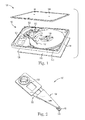
- FIG. 1 a top perspective view of a disc drive or data storage device 100 is shown.
- Storage device 100 is provided to show an exemplary environment in which various embodiments of the present invention can be practiced. It will be understood, however, that the claimed invention is not so limited.
- Device 100 includes a sealed housing 102 formed from a base deck 104 and top cover 106.
- a spindle motor 108 is configured to rotate at least one storage medium such as a disc, in many embodiments multiple storage media or discs 110.
- Discs 110 are accessed by a corresponding array of data transducers that are each supported by a head gimbal assembly (HGA) 112. While FIG. 1 shows the use of two magnetic recording discs and four corresponding heads, other numbers of heads and discs (such as a single disc, etc.) and other types of media (such as optical media, etc.) can alternatively be utilized as desired.
- HGA head gimbal assembly
- Each HGA 112 is preferably supported by a head-stack assembly 114 (also referred to as an actuator) that includes a flexible suspension assembly 116, which in turn is supported by a rigid actuator arm 118.
- Actuator 114 pivots about a cartridge bearing assembly 120 through application of current to a voice coil motor (VCM) 122.
- VCM voice coil motor
- controlled operation of VCM 122 causes the transducers of HGA 112 to align with tracks (not shown) defined on the disc surfaces to store data thereto or retrieve data therefrom.
- a printed circuit cable 124 provides electrical communication between actuator 114 and device control electronics on an externally disposed device printed circuit board (PCB) 126.
- PCB printed circuit board
- Printed circuit cable 124 can include multiple circuits that allow communication of several different components of device 100 with PCB 126.
- FIG. 2 shows an exemplary actuator 130 that can be used in the data storage device of FIG. 1 , where actuator is identified as element 114.
- Actuator 130 has a base 132 supporting a load beam 134 via a preload bend section 136; together, base 132, load beam 134 and section 136 form a rigid arm, such as actuator arm 118 of FIG. 1 .
- An HGA 140 (identified as HGA 112 in FIG. 1 ) is supported at the distal end of the load beam 134 and includes a data transducer or head gimbaled for multi-axial rotation along pitch (x-axis) and roll (y-axis) directions via a gimbal plate 142 and dimple (not separately shown).
- HGA 140 includes a slider having a bearing surface facing the associated disc surface.
- the bearing surface interacts with fluidic currents established by high speed rotation of the disc surface to hydrodynamically support the slider adjacent the surface.
- Such bearing surfaces are often referred to as "air bearing” surfaces even when a different fluid other than atmospheric air (e.g., an inert gas such as a helium) is retained within housing 102 of device 100.
- Read and write data transducing elements are mounted to the slider such as along a trailing edge thereof to transduce data from/to the media surface. Controlled articulation of the slider is implemented by incorporating a microactuator into HGA 140.
- HGA 140 has a gimbal plate 142 configured with an aperture 144 that extends through the thickness of the plate 142.
- a gimbal island 146 is disposed within aperture 144 of gimbal plate 142, and is a separate member not mechanically coupled to plate 142. That is, the gimbal island 146 is mechanically decoupled from the gimbal plate 142 to allow the island 146 to move independently of the plate 142 as will be discussed below.
- HGA 140 includes a flex circuit 148 capable of transferring electric signals to electrodes (not shown) on gimbal island 146.
- the entire length of flex circuit 148 is elastic and can maintain multiple circuit pathways that may correspond to independent circuits and interconnected circuits that are connected to components of HGA 140 by one or more electrodes.
- six independent circuits are located on flex circuit 148 and have six corresponding electrodes (not shown) that can be electrically interconnected to a single component, such as a data transducing head, or multiple components, such as microactuators.
- each microactuator 150 is constructed of a piezoelectric (PZT) material and is connected to a portion of flex circuit 148. While the size, composition, and configuration of microactuators 150 is not limited, attachment of microactuators 150 to both gimbal island 146 and plate 142 can allow island 146 to be deflected by corresponding movement of one or both microactuators 150. The movement of microactuators 150 thus moves, pivots and twists slider 152 as appropriate so that the magnetic and/or optical transducing components of slider 152 are aligned to read data from and/or write data to a storage medium such as disc 110 of FIG. 1 .
- PZT piezoelectric
- FIG. 4 illustrates one embodiment of a thin film PZT microactuator 160.
- Microactuator 160 has a thin film PZT layer 162 sandwiched by a first, bottom electrode 164 and a second, top electrode 166, all which is supported on a silicon substrate 168.
- PZT layer 162 is present on only a section of bottom electrode 164, leaving a second and/or third section of bottom electrode 164 uncovered by PZT layer 162.
- a dielectric material 170 is present between bottom electrode 164 and substrate 168.
- the "bottom electrode” is the electrode closer to the substrate than the "top layer”; this convention of “top” and “bottom,” where “bottom” is closer to the substrate than the “top,” is used consistently throughout this disclosure.
- a passivation layer 172 covers and preferably envelops PZT layer 162 and electrodes 164, 166. Passivation layer 172 provides physical and chemical protection to PZT layer 162 and electrodes 164, 166 from factors such as humidity, chemicals, particulate and other debris, and overall, from the surrounding environment. Electrically connected to top electrode 166 is top metal pad 176 and electrically connected to bottom electrode 164 (specifically, to the section of bottom electrode 164 not covered by PZT layer 162) is a bottom metal pad 174.
- suitable materials for electrodes 164, 166 include noble metals such as platinum (Pt), iridium (Ir), ruthenium (Ru), rhodium (Rh), and alloys thereof.
- Other suitable materials for electrodes 164, 166 include oxides such as strontium titanium oxide (STO or SrTiO 3 ) and lanthanum nickel oxide (LNO).
- Top electrode 164 may be the same or different material than bottom electrode 166.
- Metal pads 174, 176 are electrically conducting and provide electrical contact from electrodes 144, 146 to appropriate circuitry. Suitable materials for metal pads 174, 176 include gold (Au), silver (Ag), and copper (Cu).
- Passivation layer 172 may be an electrically insulating material, although in some embodiments, passivation layer 172 is a dielectric material.
- materials suitable for passivation layer 172 include carbon, silicon dioxide or silica (SiO 2 ) (including different types of materials containing SiO 2 made by different techniques, e.g., high density plasma (HDP), chemical vapor deposition (CVD), flowable oxide (FOX), boron doped silicate glass (BSG), phosphorous doped silicate glass (PSG), borophosphosilicate glass (BPSG)), tetra-ethyl-ortho-silicate or tetra-ethoxy-silane (TEOS), aluminum oxide or alumina (Al 2 O 3 ), titanium nitride (TiN), titanium sub-oxide (TiO x ), titanium carbide (TiC), silicon nitride (Si 3 N 4 ), silicon oxynitride (SiO x N y
- an adhesion layer is present among the layers of microactuator 160, to improve the adhesion of passivation layer 172 to the other layers of microactuator 160.
- suitable materials for the adhesion layer include titanium (Ti), tantalum (Ta), chromium (Cr), alloys thereof and mixtures thereof.
- a method for forming a microactuator with a passivation layer enhanced by an adhesion layer is outlined in FIG. 5 ; in this method, the adhesion between the top electrode and the dielectric passivation layer is increased.
- a bottom electrode e.g., electrode 166
- a PZT layer is deposited directly onto the bottom electrode from step 180.
- a top electrode e.g., electrode 164
- step 183 an adhesion layer is positioned over the electrode from step 182.
- step 184 a mask is applied over the adhesion layer and the top electrode.
- the top electrode layer functions as a hard mask to etch the PZT layer.
- the unmasked areas of the adhesion layer and the top electrode are etched in step 185; the resulting exposed PZT material is etched in step 186.
- step 187 a mask is deposited over the structure, particularly the top electrode, and patterned. The unmasked areas of the adhesion layer and the top electrode are etched in step 188, thus forming the top electrode.
- a poly(methyl glutarimide) (PMGI) photoresist mask is patterned over the PZT layer and top electrode, forming a mask for the subsequent adhesion layer lift-off process.
- An adhesion layer is deposited over the structure, including the photoresist, in step 190, and the photoresist is removed in step 191, together with the adhesion layer present on the photoresist; any adhesion layer not having photoresist there below remains.
- a patterned mask is deposited over the exposed bottom electrode, and the bottom electrode and adhesion layer are etched in step 193.
- a passivation layer is deposited in step 194 over the structure in step 194.
- a patterned mask is deposited over the passivation layer, and the passivation layer is etched in step 196.
- FIGS. 6A-6E illustrate an exemplary lift-off process of the adhesion layer.
- a lift-off process is a simple, easy method for patterning deposited firms.
- a pattern is defined on a substrate using photoresist.
- a film, such as a metallic film, is blanket-deposited over the substrate, covering the photoresist and areas in which the photoresist has been removed.
- the photoresist under the film is removed with solvent, taking the film with in, and leaving only the film that was deposited on the substrate.
- FIG. 6A shows a silicon substrate 200 having a dielectric layer 201 thereon.
- a first, bottom electrode 202, a PZT layer 203 and a second, top electrode 204 are arranged on substrate 200 and dielectric 201.
- Overlying top electrode 204 is an adhesion layer 206.
- the stack composed of PZT layer 203, electrode 204 and adhesion layer 206 is covered on its top and sides by a first layer of photoresist 208 in FIG. 6B .
- Photoresist layer 208 surrounds the stack, so that no portion of PZT layer 203, electrode 204 and adhesion layer 206 is exposed.
- first photoresist layer 208 Deposited over first photoresist layer 208 is a second photoresist layer 210, which may be deposited subsequently to or simultaneously with layer 208.
- the materials and/or thickness of photoresist layers 208, 210 are selected so that when photoresists 208, 210 are cured and patterned, second photoresist layer 210 etches faster than first photoresist layer 208, resulting in the structure of FIG. 6B .
- the thick second photoresist 210 does not extend to electrode 202.
- a second adhesion layer 212 is deposited over the entire surface in FIG.
- adhesion layer portion 212A present on bottom electrode 202 and adhesion layer portion 212B present on second photoresist 210.
- second photoresist 210 has been removed together with adhesion layer portion 212B and first photoresist 208, leaving adhesion layer portions 212A and adhesion layer 206 exposed.
- an area of bottom electrode 202 is exposed and not covered by adhesion layer portion 212A, due to that area having been shadowed by second photoresist 210.
- a passivation layer 214 is applied over the entire structure. The resulting structure has adhesion layer portion 212A present between bottom electrode 202 and passivation layer 214, and adhesion layer 206 present between top electrode 204 and passivation layer 214.
- FIGS. 7A-7F illustrate another process for forming a microactuator with a passivation layer enhanced by an adhesion layer.
- FIG. 7A shows a silicon substrate 220 having a dielectric layer 221, a first, bottom electrode 222, and an adhesion layer 223 thereon.
- the adhesion layer is patterned to form two adhesion layer sections 223A and 223B with a gap or hole therebetween, and a portion of bottom electrode 222 exposed in the gap.
- FIG. 7C the gap between adhesion layer sections 223A, 223B is filled with PZT 224.
- a top electrode 226 is formed over PZT 224 in FIG. 7D
- a top adhesion layer 228 is formed in FIG. 7E .
- FIG. 7F the entire structure is covered with passivation layer 230.
- the resulting structure has adhesion layer sections 223A, 223B present between bottom electrode 222 and passivation layer 230, and adhesion layer 228 present between top electrode 226 and passivation layer 230.
- silicon substrate 200, 220 may be a silicon-based substrate, such as a conventional Si wafer. In other embodiments, a non-silicon semiconductor material may be used for the substrate. Dielectric layer 201, 221 is generally present in the structure of this disclosure, however, it is optional.
- Electrodes 202, 204, 222, 226 are composed of noble metals such as platinum (Pt), iridium (Ir), ruthenium (Ru), rhodium (Rh), and alloys thereof, or oxides such as strontium titanium oxide (STO or SrTiO 3 ) and lanthanum nickel oxide (LNO). Electrodes 202, 204, 222, 226 each typically have a thickness of 50 to 100 nm, although thinner and thicker electrodes 202, 204, 222, 226 could be used. Electrodes 202, 204, 222, 226 may be of the same or different material, and have the same or different thicknesses.
- adhesion layer 206, 223A, 223B and adhesion layer portions 212A, 212B are composed of metal, such as titanium (Ti), tantalum (Ta) or chromium (Cr), although other metals or metal alloys could be used.
- the selection of the adhesion layer material is based on the adhesion coefficient of the adhesion material to the passivation layer, which is typically a dielectric material.
- Adhesion layer 206, 223A, 223B and portions 212A, 212B each typically have a thickness of 1 to 50 nm, in some embodiments 5 to 15 nm (e.g., 10 nm), although thinner and thicker adhesion layer 206, 223A, 223B and portions 212A, 212B could be used.
- Adhesion layer 206, 223A, 223B and portions 212A, 212B may be of the same or different material, and have the same or different thicknesses.
- passivation layer 214, 230 may be an electrically insulating material or a dielectric material.
- materials suitable for passivation layer 214, 230 include carbon, silicon dioxide or silica (SiO 2 ), tetra-ethyl-ortho-silicate or tetra-ethoxy-silane (TEOS), aluminum oxide or alumina (Al 2 O 3 ), titanium nitride (TiN), titanium sub-oxide (TiO x ), titanium carbide (TiC), silicon nitride (Si 3 N 4 ), silicon oxynitride (SiO x N y ), and silicon nitride oxide (Si 2 N 2 O).
- Passivation layer 214, 230 can be applied, for example, by plasma deposition, dielectric deposition, chemical vapor deposition (including plasma enhanced chemical vapor deposition, or PECVD). Passivation layer 214, 230 typically has a thickness of less than one micrometer, usually 0.2 to 0.7 micrometer (e.g., 0.5 micrometer).
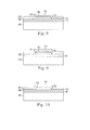
- FIGS. 8, 9 and 10 illustrate three microactuator constructions having an adhesion layer to improve the adhesion of the passivation layer.
- adhesion layer material is present between the passivation layer and the top electrode and the bottom electrode.
- adhesion layer material is present between the passivation layer and the top electrode, but is not present over the bottom electrode.
- adhesion layer material is present between the passivation layer and the bottom electrode, but is not present over the top electrode.
- FIG. 8 The structure of FIG. 8 is the same as the structure of FIG. 6E , having stacked substrate 200, dielectric 201, bottom electrode 202, PZT 203 and top electrode 204.
- a bottom adhesion layer 212 contacts bottom electrode 202 and a top adhesion layer 206 contacts top electrode 206.
- a portion of bottom electrode 202 is not covered by adhesion layer 212; this is due to the process of making the structure, and other processes will provide a structure with bottom electrode fully covered by the adhesion layer.
- Overlying bottom adhesion layer 212 and top adhesion layer 206 is passivation layer 214.
- stacked on substrate 300 are dielectric 301, bottom electrode 302, PZT 303 and top electrode 304.
- a top adhesion layer 306 contacts top electrode 306.
- no portion of bottom electrode 302 is covered by an adhesion layer.
- stacked on substrate 400 are dielectric 401, bottom electrode 402, PZT 403 and top electrode 404.
- bottom electrode 402 Over and contacting bottom electrode 402 is a bottom adhesion layer 412. In this embodiment, no portion of top electrode 404 is covered by an adhesion layer.
- passivation layer 414 Overlying bottom adhesion layer 412 and top electrode 404 is passivation layer 414.
Landscapes
- Engineering & Computer Science (AREA)
- Manufacturing & Machinery (AREA)
- Supporting Of Heads In Record-Carrier Devices (AREA)
- Micromachines (AREA)
- Moving Of The Head To Find And Align With The Track (AREA)
Abstract
Description
- Hard disc drive systems (HDDs) typically include one or more data storage discs. A transducing head carried by a slider is used to read from and write to a data track on a disc. A head gimbal assembly (HGA) allows precise positioning of the data transducer head adjacent the tracks by allowing the transducer to gimbal along multiple axes to follow the topography of the media surface. The microactuator reduces resonance modes of the HGA and provides second order positional control capabilities. Microactuators can be formed from piezoelectric (PZT) or other materials to induce controlled rotation of the HGA transducer. While operable, limitations associated with current microactuator designs can include the need for increased HGA stack heights, the introduction of asymmetric drive and resonance characteristics, increased HGA preload force concentrations, and the need for an additional interposer structure in the HGA to separately route the electrical control signals to the microactuator and the slider.
- The present disclosure provides improvements for head gimbal assemblies, by providing protection for the microactuator by way of a passivation layer. This disclosure provides several structures having enhanced adhesion of the passivation layer to the microactuator and methods of making those structures.
- One particular embodiment of this disclosure is a microactuator comprising a substrate, a sandwich structure on the substrate, and a passivation layer over the substrate and the sandwich structure. The sandwich structure has a bottom electrode formed from a noble metal, a piezoelectric layer, and a top electrode formed from a noble metal. The microactuator further has one or both of a bottom adhesion layer present between the bottom electrode and the passivation layer, and a top adhesion layer present between the top electrode and the passivation layer. That is, the microactuator may have only the bottom adhesion layer, only the top adhesion layer, or both the bottom adhesion layer and the top adhesion layer.
- Another particular embodiment of this disclosure is a microactuator comprising a silicon substrate, a bottom electrode on the substrate, a piezoelectric layer on and in contact with a first section of the bottom electrode, a top electrode on and in contact with the piezoelectric layer, a bottom adhesion layer on a second section of the bottom electrode, a top adhesion layer on the top electrode, and a passivation layer over the bottom adhesion layer and the top adhesion layer.
- Yet another particular embodiment of this disclosure is a disc drive comprising a microactuator, a suspension assembly, and a head gimbal assembly. The microactuator can have a silicon substrate, a bottom electrode comprising one of platinum, iridium, ruthenium, or rhodium on the substrate, a piezoelectric layer on and in contact with a first section of the bottom electrode, a top electrode comprising one of platinum, iridium, ruthenium, or rhodium, on and in contact with the piezoelectric layer, a bottom adhesion layer on a second section of the bottom electrode, a top adhesion layer on the top electrode, and a dielectric passivation layer over the bottom adhesion layer and the top adhesion layer.
- These and various other features and advantages will be apparent from a reading of the following detailed description.
- The disclosure may be more completely understood in consideration of the following detailed description of various embodiments of the disclosure in connection with the accompanying drawing, in which:
-
FIG. 1 is an exploded, perspective view of a data storage device. -
FIG. 2 is a perspective view of a suspension portion of the data storage device ofFIG. 1 . -
FIG. 3 is a perspective view of a head gimbal assembly of the suspension portion ofFIG. 2 . -
FIG. 4 is a schematic side view of a microactuator. -
FIG. 5 is a block diagram of a method for forming a microactuator having a passivation layer and an adhesion layer. -
FIGS. 6A-6E illustrate, step-wise, the method ofFIG. 5 for forming a microactuator having a passivation layer and an adhesion layer. -
FIGS. 7A-7F illustrate, step-wise, another method for forming a microactuator having a passivation layer and an adhesion layer. -
FIG. 8 is a schematic side view of a microactuator having a passivation layer and an adhesion layer. -
FIG. 9 is a schematic side view of another embodiment of a microactuator having a passivation layer and an adhesion layer. -
FIG. 10 is a schematic side view of another embodiment of a microactuator having a passivation layer and an adhesion layer. - The present embodiments relate most generally to microactuator-based head gimbal assemblies (HGAs). Disclosed are improvements for protecting head gimbal assemblies, by providing a passivation layer over the piezoelectric (PZT) material. This disclosure provides several structures having enhanced adhesion of the passivation layer to the microactuator and methods of making those structures.
- In the following description, reference is made to the accompanying drawing that forms a part hereof and in which are shown by way of illustration at least one specific embodiment. The following description provides additional specific embodiments. It is to be understood that other embodiments are contemplated and may be made without departing from the scope or spirit of the present disclosure. The following detailed description, therefore, is not to be taken in a limiting sense. While the present disclosure is not so limited, an appreciation of various aspects of the disclosure will be gained through a discussion of the examples provided below.
- Unless otherwise indicated, all numbers expressing feature sizes, amounts, and physical properties are to be understood as being modified by the term "about." Accordingly, unless indicated to the contrary, the numerical parameters set forth are approximations that can vary depending upon the desired properties sought to be obtained by those skilled in the art utilizing the teachings disclosed herein.
- As used herein, the singular forms "a", "an", and "the" encompass embodiments having plural referents, unless the content clearly dictates otherwise. As used in this specification and the appended claims, the term "or" is generally employed in its sense including "and/or" unless the content clearly dictates otherwise.
- Spatially related terms, including but not limited to, "lower", "upper", "beneath", "below", "above", "on top", etc., if used herein, are utilized for ease of description to describe spatial relationships of an element(s) to another. Such spatially related terms encompass different orientations of the device in addition to the particular orientations depicted in the figures and described herein. For example, if a structure depicted in the figures is turned over or flipped over, portions previously described as below or beneath other elements would then be above those other elements.
- Referring to
FIG. 1 , a top perspective view of a disc drive ordata storage device 100 is shown.Storage device 100 is provided to show an exemplary environment in which various embodiments of the present invention can be practiced. It will be understood, however, that the claimed invention is not so limited. -
Device 100 includes a sealedhousing 102 formed from abase deck 104 andtop cover 106. Aspindle motor 108 is configured to rotate at least one storage medium such as a disc, in many embodiments multiple storage media ordiscs 110.Discs 110 are accessed by a corresponding array of data transducers that are each supported by a head gimbal assembly (HGA) 112. WhileFIG. 1 shows the use of two magnetic recording discs and four corresponding heads, other numbers of heads and discs (such as a single disc, etc.) and other types of media (such as optical media, etc.) can alternatively be utilized as desired. - Each HGA 112 is preferably supported by a head-stack assembly 114 (also referred to as an actuator) that includes a
flexible suspension assembly 116, which in turn is supported by arigid actuator arm 118.Actuator 114 pivots about a cartridge bearingassembly 120 through application of current to a voice coil motor (VCM) 122. In this way, controlled operation ofVCM 122 causes the transducers ofHGA 112 to align with tracks (not shown) defined on the disc surfaces to store data thereto or retrieve data therefrom. - A
printed circuit cable 124 provides electrical communication betweenactuator 114 and device control electronics on an externally disposed device printed circuit board (PCB) 126. Printedcircuit cable 124 can include multiple circuits that allow communication of several different components ofdevice 100 with PCB 126. -
FIG. 2 shows anexemplary actuator 130 that can be used in the data storage device ofFIG. 1 , where actuator is identified aselement 114. Actuator 130 has abase 132 supporting aload beam 134 via apreload bend section 136; together,base 132,load beam 134 andsection 136 form a rigid arm, such asactuator arm 118 ofFIG. 1 . An HGA 140 (identified as HGA 112 inFIG. 1 ) is supported at the distal end of theload beam 134 and includes a data transducer or head gimbaled for multi-axial rotation along pitch (x-axis) and roll (y-axis) directions via agimbal plate 142 and dimple (not separately shown). - HGA 140 includes a slider having a bearing surface facing the associated disc surface. The bearing surface interacts with fluidic currents established by high speed rotation of the disc surface to hydrodynamically support the slider adjacent the surface. Such bearing surfaces are often referred to as "air bearing" surfaces even when a different fluid other than atmospheric air (e.g., an inert gas such as a helium) is retained within
housing 102 ofdevice 100. Read and write data transducing elements are mounted to the slider such as along a trailing edge thereof to transduce data from/to the media surface. Controlled articulation of the slider is implemented by incorporating a microactuator intoHGA 140. - An
exemplary HGA 140 is shown inFIG. 3 .HGA 140 has agimbal plate 142 configured with anaperture 144 that extends through the thickness of theplate 142. Agimbal island 146 is disposed withinaperture 144 ofgimbal plate 142, and is a separate member not mechanically coupled toplate 142. That is, thegimbal island 146 is mechanically decoupled from thegimbal plate 142 to allow theisland 146 to move independently of theplate 142 as will be discussed below. -
HGA 140 includes a flex circuit 148 capable of transferring electric signals to electrodes (not shown) ongimbal island 146. In some embodiments, the entire length of flex circuit 148 is elastic and can maintain multiple circuit pathways that may correspond to independent circuits and interconnected circuits that are connected to components ofHGA 140 by one or more electrodes. In the illustrated embodiment, six independent circuits are located on flex circuit 148 and have six corresponding electrodes (not shown) that can be electrically interconnected to a single component, such as a data transducing head, or multiple components, such as microactuators. -
HGA 140 has twomicroactuators 150 and aslider 152. In various embodiments, eachmicroactuator 150 is constructed of a piezoelectric (PZT) material and is connected to a portion of flex circuit 148. While the size, composition, and configuration ofmicroactuators 150 is not limited, attachment ofmicroactuators 150 to bothgimbal island 146 andplate 142 can allowisland 146 to be deflected by corresponding movement of one or bothmicroactuators 150. The movement ofmicroactuators 150 thus moves, pivots and twistsslider 152 as appropriate so that the magnetic and/or optical transducing components ofslider 152 are aligned to read data from and/or write data to a storage medium such asdisc 110 ofFIG. 1 . - As track densities on
disc 100 increase, precise control byHGA 140 is required, in order forslider 152 to be properly positioned. The precision ofmicroactuators 150 is critical forpositioning slider 152.FIG. 4 illustrates one embodiment of a thinfilm PZT microactuator 160. -
Microactuator 160 has a thinfilm PZT layer 162 sandwiched by a first,bottom electrode 164 and a second,top electrode 166, all which is supported on asilicon substrate 168. As can be seen inFIG. 4 ,PZT layer 162 is present on only a section ofbottom electrode 164, leaving a second and/or third section ofbottom electrode 164 uncovered byPZT layer 162. Adielectric material 170 is present betweenbottom electrode 164 andsubstrate 168. As used throughout this disclosure, the "bottom electrode" is the electrode closer to the substrate than the "top layer"; this convention of "top" and "bottom," where "bottom" is closer to the substrate than the "top," is used consistently throughout this disclosure. Apassivation layer 172 covers and preferably envelopsPZT layer 162 andelectrodes Passivation layer 172 provides physical and chemical protection toPZT layer 162 andelectrodes top electrode 166 istop metal pad 176 and electrically connected to bottom electrode 164 (specifically, to the section ofbottom electrode 164 not covered by PZT layer 162) is abottom metal pad 174. - Examples of suitable materials for
electrodes electrodes Top electrode 164 may be the same or different material thanbottom electrode 166. -
Metal pads electrodes metal pads -
Passivation layer 172 may be an electrically insulating material, although in some embodiments,passivation layer 172 is a dielectric material. Examples of materials suitable forpassivation layer 172 include carbon, silicon dioxide or silica (SiO2) (including different types of materials containing SiO2 made by different techniques, e.g., high density plasma (HDP), chemical vapor deposition (CVD), flowable oxide (FOX), boron doped silicate glass (BSG), phosphorous doped silicate glass (PSG), borophosphosilicate glass (BPSG)), tetra-ethyl-ortho-silicate or tetra-ethoxy-silane (TEOS), aluminum oxide or alumina (Al2O3), titanium nitride (TiN), titanium sub-oxide (TiOx), titanium carbide (TiC), silicon nitride (Si3N4), silicon oxynitride (SiOxNy), and silicon nitride oxide (Si2N2O). - In accordance with this disclosure, an adhesion layer is present among the layers of
microactuator 160, to improve the adhesion ofpassivation layer 172 to the other layers ofmicroactuator 160. Examples of suitable materials for the adhesion layer include titanium (Ti), tantalum (Ta), chromium (Cr), alloys thereof and mixtures thereof. - One embodiment of a method for forming a microactuator with a passivation layer enhanced by an adhesion layer is outlined in
FIG. 5 ; in this method, the adhesion between the top electrode and the dielectric passivation layer is increased. Instep 180, a bottom electrode (e.g., electrode 166) is deposited, for example, on a silicon substrate (e.g., Si wafer) or on a dielectric material. Instep 181, a PZT layer is deposited directly onto the bottom electrode fromstep 180. A top electrode (e.g., electrode 164) is deposited instep 183 directly onto the PZT layer fromstep 181. There is no intermediate or intervening layer between either electrode and the PZT layer. Instep 183, an adhesion layer is positioned over the electrode fromstep 182. Instep 184, a mask is applied over the adhesion layer and the top electrode. At this step in the process, the top electrode layer functions as a hard mask to etch the PZT layer. The unmasked areas of the adhesion layer and the top electrode are etched instep 185; the resulting exposed PZT material is etched instep 186. Subsequently, instep 187, a mask is deposited over the structure, particularly the top electrode, and patterned. The unmasked areas of the adhesion layer and the top electrode are etched instep 188, thus forming the top electrode. Instep 189, a poly(methyl glutarimide) (PMGI) photoresist mask is patterned over the PZT layer and top electrode, forming a mask for the subsequent adhesion layer lift-off process. An adhesion layer is deposited over the structure, including the photoresist, instep 190, and the photoresist is removed instep 191, together with the adhesion layer present on the photoresist; any adhesion layer not having photoresist there below remains. Instep 192, a patterned mask is deposited over the exposed bottom electrode, and the bottom electrode and adhesion layer are etched instep 193. A passivation layer is deposited instep 194 over the structure instep 194. Instep 195, a patterned mask is deposited over the passivation layer, and the passivation layer is etched instep 196. -
FIGS. 6A-6E illustrate an exemplary lift-off process of the adhesion layer. In general, a lift-off process is a simple, easy method for patterning deposited firms. A pattern is defined on a substrate using photoresist. A film, such as a metallic film, is blanket-deposited over the substrate, covering the photoresist and areas in which the photoresist has been removed. During the actual lifting-off process, the photoresist under the film is removed with solvent, taking the film with in, and leaving only the film that was deposited on the substrate. -
FIG. 6A shows asilicon substrate 200 having adielectric layer 201 thereon. A first,bottom electrode 202, aPZT layer 203 and a second,top electrode 204 are arranged onsubstrate 200 and dielectric 201. Overlyingtop electrode 204 is anadhesion layer 206. The stack composed ofPZT layer 203,electrode 204 andadhesion layer 206 is covered on its top and sides by a first layer ofphotoresist 208 inFIG. 6B .Photoresist layer 208 surrounds the stack, so that no portion ofPZT layer 203,electrode 204 andadhesion layer 206 is exposed. Deposited overfirst photoresist layer 208 is asecond photoresist layer 210, which may be deposited subsequently to or simultaneously withlayer 208. The materials and/or thickness ofphotoresist layers photoresists second photoresist layer 210 etches faster thanfirst photoresist layer 208, resulting in the structure ofFIG. 6B . In the embodiment illustrated inFIG. 6B , the thicksecond photoresist 210 does not extend to electrode 202. Asecond adhesion layer 212 is deposited over the entire surface inFIG. 6C , resulting inadhesion layer portion 212A present onbottom electrode 202 andadhesion layer portion 212B present onsecond photoresist 210. InFIG. 6D ,second photoresist 210 has been removed together withadhesion layer portion 212B andfirst photoresist 208, leavingadhesion layer portions 212A andadhesion layer 206 exposed. In the embodiment ofFIG. 6D , an area ofbottom electrode 202 is exposed and not covered byadhesion layer portion 212A, due to that area having been shadowed bysecond photoresist 210. InFIG. 6E , apassivation layer 214 is applied over the entire structure. The resulting structure hasadhesion layer portion 212A present betweenbottom electrode 202 andpassivation layer 214, andadhesion layer 206 present betweentop electrode 204 andpassivation layer 214. -
FIGS. 7A-7F illustrate another process for forming a microactuator with a passivation layer enhanced by an adhesion layer. -
FIG. 7A shows asilicon substrate 220 having adielectric layer 221, a first,bottom electrode 222, and anadhesion layer 223 thereon. InFIG. 7B , the adhesion layer is patterned to form twoadhesion layer sections bottom electrode 222 exposed in the gap. InFIG. 7C , the gap betweenadhesion layer sections PZT 224. Atop electrode 226 is formed overPZT 224 inFIG. 7D , and atop adhesion layer 228 is formed inFIG. 7E . InFIG. 7F , the entire structure is covered withpassivation layer 230. The resulting structure hasadhesion layer sections bottom electrode 222 andpassivation layer 230, andadhesion layer 228 present betweentop electrode 226 andpassivation layer 230. - As indicated above,
silicon substrate Dielectric layer -
Electrodes Electrodes thicker electrodes Electrodes - Also as indicated above,
adhesion layer adhesion layer portions Adhesion layer portions thicker adhesion layer portions Adhesion layer portions - Also as indicated above,
passivation layer passivation layer Passivation layer Passivation layer -
FIGS. 8, 9 and 10 illustrate three microactuator constructions having an adhesion layer to improve the adhesion of the passivation layer. InFIG. 8 , adhesion layer material is present between the passivation layer and the top electrode and the bottom electrode. InFIG. 9 , adhesion layer material is present between the passivation layer and the top electrode, but is not present over the bottom electrode. InFIG. 10 , adhesion layer material is present between the passivation layer and the bottom electrode, but is not present over the top electrode. - The structure of
FIG. 8 is the same as the structure ofFIG. 6E , having stackedsubstrate 200, dielectric 201,bottom electrode 202,PZT 203 andtop electrode 204. Abottom adhesion layer 212 contactsbottom electrode 202 and atop adhesion layer 206 contactstop electrode 206. In this embodiment, a portion ofbottom electrode 202 is not covered byadhesion layer 212; this is due to the process of making the structure, and other processes will provide a structure with bottom electrode fully covered by the adhesion layer. Overlyingbottom adhesion layer 212 andtop adhesion layer 206 ispassivation layer 214. - In
FIG. 9 , stacked onsubstrate 300 are dielectric 301,bottom electrode 302,PZT 303 andtop electrode 304. Atop adhesion layer 306 contactstop electrode 306. In this embodiment, no portion ofbottom electrode 302 is covered by an adhesion layer. Overlyingbottom electrode 302 andtop adhesion layer 306 ispassivation layer 314. - In
FIG. 10 , stacked onsubstrate 400 are dielectric 401,bottom electrode 402,PZT 403 andtop electrode 404. Over and contactingbottom electrode 402 is abottom adhesion layer 412. In this embodiment, no portion oftop electrode 404 is covered by an adhesion layer. Overlyingbottom adhesion layer 412 andtop electrode 404 ispassivation layer 414. - Thus, embodiments of the ADHESION ENHANCEMENT OF THIN FILM PZT STRUCTURE are disclosed. The implementations described above and other implementations are within the scope of the following claims. One skilled in the art will appreciate that the present invention can be practiced with embodiments other than those disclosed. The disclosed embodiments are presented for purposes of illustration and not limitation, and the present invention is limited only by the claims that follow.
Claims (20)
- A microactuator comprising:a substrate;a sandwich structure on the substrate, the sandwich structure consisting of a bottom electrode comprising a noble metal, a piezoelectric layer, and a top electrode comprising a noble metal; anda passivation layer over the substrate and the sandwich structure; the microactuator further comprising one or both of:a bottom adhesion layer present between the bottom electrode and the passivation layer; anda top adhesion layer present between the top electrode and the passivation layer.
- The microactuator of claim 1 comprising both the bottom adhesion layer and the top adhesion layer.
- The microactuator of claim 1 wherein the passivation layer comprises tetra-ethyl-ortho-silicate.
- The microactuator of claim 1 wherein the passivation layer has a thickness of less than 1 micrometer.
- The microactuator of claim 1 wherein the bottom electrode comprises platinum and the top electrode comprises ruthenium or platinum.
- The microactuator of claim 1 wherein one or both of the adhesion layers comprises titanium, tantalum or chromium.
- The microactuator of claim 6 wherein the adhesion layers have a thickness of 5 to 15 nm.
- The microactuator of claim 1 further comprising a dielectric layer between the substrate and the sandwich structure.
- A microactuator comprising:a silicon substrate;a bottom electrode on the substrate;a piezoelectric layer on and in contact with a first section of the bottom electrode;a top electrode on and in contact with the piezoelectric layer;a bottom adhesion layer on a second section of the bottom electrode;a top adhesion layer on the top electrode; anda passivation layer over the bottom adhesion layer and the top adhesion layer.
- The microactuator of claim 9 further comprising a dielectric layer on the substrate, with the bottom electrode on the dielectric layer.
- The microactuator of claim 9 wherein the bottom electrode and the top electrode each comprise a noble metal.
- The microactuator of claim 11 wherein the bottom electrode comprises platinum and the top electrode comprises ruthenium or platinum.
- The microactuator of claim 9 wherein the bottom electrode and the top electrode each individually comprises platinum, iridium, ruthenium, rhodium, alloys thereof, strontium titanium oxide, or lanthanum nickel oxide.
- The microactuator of claim 9 wherein the passivation layer comprises tetra-ethyl-ortho-silicate.
- The microactuator of claim 14 wherein the passivation layer has a thickness of less than 1 micrometer.
- The microactuator of claim 9 wherein one or both of the adhesion layers comprises titanium, tantalum or chromium.
- The microactuator of claim 9 wherein the adhesion layers have a thickness of 5 to 15 nm.
- A disc drive comprising a microactuator, a suspension assembly, and a head gimbal assembly; the microactuator comprising a silicon substrate, a bottom electrode comprising one of platinum, iridium, ruthenium, or rhodium on the substrate, a piezoelectric layer on and in contact with a first section of the bottom electrode, a top electrode comprising one of platinum, iridium, ruthenium, or rhodium, on and in contact with the piezoelectric layer, a bottom adhesion layer on a second section of the bottom electrode, a top adhesion layer on the top electrode, and a dielectric passivation layer over the bottom adhesion layer and the top adhesion layer.
- The disc drive of claim 18 wherein the passivation layer comprises tetra-ethyl-ortho-silicate.
- The disc drive of claim 18 wherein one or both of the adhesion layers comprises titanium, tantalum or chromium.
Applications Claiming Priority (1)
| Application Number | Priority Date | Filing Date | Title |
|---|---|---|---|
| US13/886,780 US8854772B1 (en) | 2013-05-03 | 2013-05-03 | Adhesion enhancement of thin film PZT structure |
Publications (1)
| Publication Number | Publication Date |
|---|---|
| EP2800095A1 true EP2800095A1 (en) | 2014-11-05 |
Family
ID=50630658
Family Applications (1)
| Application Number | Title | Priority Date | Filing Date |
|---|---|---|---|
| EP14166801.2A Withdrawn EP2800095A1 (en) | 2013-05-03 | 2014-05-01 | Adhesion enhancement of thin film PZT structure |
Country Status (5)
| Country | Link |
|---|---|
| US (1) | US8854772B1 (en) |
| EP (1) | EP2800095A1 (en) |
| JP (1) | JP2014225317A (en) |
| KR (1) | KR101552279B1 (en) |
| CN (1) | CN104218146A (en) |
Cited By (1)
| Publication number | Priority date | Publication date | Assignee | Title |
|---|---|---|---|---|
| US11152024B1 (en) | 2020-03-30 | 2021-10-19 | Western Digital Technologies, Inc. | Piezoelectric-based microactuator arrangement for mitigating out-of-plane force and phase variation of flexure vibration |
Families Citing this family (3)
| Publication number | Priority date | Publication date | Assignee | Title |
|---|---|---|---|---|
| US9786308B1 (en) | 2016-06-07 | 2017-10-10 | Seagate Technology Llc | Interconnect interposer attachable to a trailing edge of a slider |
| CN112201280B (en) * | 2019-07-08 | 2024-07-09 | 马格内康普公司 | Multilayer actuator electrode configuration for resonance improvement |
| WO2022118575A1 (en) | 2020-12-01 | 2022-06-09 | ローム株式会社 | Transducer |
Citations (8)
| Publication number | Priority date | Publication date | Assignee | Title |
|---|---|---|---|---|
| EP1367658A1 (en) * | 2001-12-18 | 2003-12-03 | Matsushita Electric Industrial Co., Ltd. | Piezoelectric element, ink jet head, angular velocity sensor, manufacturing method thereof, and ink jet type recording apparatus |
| US20050195531A1 (en) * | 2004-03-03 | 2005-09-08 | Tdk Corporation | Suspension assembly, hard disk drive, and method of manufacturing suspension assembly |
| WO2007093921A2 (en) * | 2006-02-14 | 2007-08-23 | Delphi Technologies, Inc. | Barrier coatings for a piezoelectric device |
| WO2007119174A2 (en) * | 2006-02-14 | 2007-10-25 | Delphi Technologies, Inc. | Piezoelectric actuator |
| US20120212108A1 (en) * | 2011-02-23 | 2012-08-23 | Stanley Electric Co., Ltd. | PIEZOELECTRIC ACTUATOR INCLUDING X-GRADED TiOX ADHESIVE LAYER AND ITS MANUFACTURING METHOD |
| US8310790B1 (en) * | 2011-06-11 | 2012-11-13 | Nhk Spring Co., Ltd | Remote drive rotary head dual stage actuator |
| US20120287536A1 (en) * | 2011-05-11 | 2012-11-15 | Tdk Corporation | Head support mechanism |
| US8422172B1 (en) * | 2010-10-01 | 2013-04-16 | Western Digital Technologies, Inc. | Actuator trace through a die |
Family Cites Families (15)
| Publication number | Priority date | Publication date | Assignee | Title |
|---|---|---|---|---|
| JPH1027446A (en) * | 1996-07-08 | 1998-01-27 | Nec Corp | Carriage mechanism and magnetic disk device provided therewith |
| GB2324882B (en) | 1997-04-29 | 2001-05-23 | Daewoo Electronics Co Ltd | Array of thin film actuated mirrors and method for the manufacture thereof |
| JP4501170B2 (en) * | 1999-03-18 | 2010-07-14 | ソニー株式会社 | Semiconductor device and manufacturing method thereof |
| US6799820B1 (en) * | 1999-05-20 | 2004-10-05 | Seiko Epson Corporation | Liquid container having a liquid detecting device |
| JP4362859B2 (en) * | 2001-01-26 | 2009-11-11 | セイコーエプソン株式会社 | Inkjet recording head and printer |
| JP2007200534A (en) * | 2006-01-26 | 2007-08-09 | Shinka Jitsugyo Kk | Slider for high density magnetic recording |
| JP2008173924A (en) * | 2007-01-22 | 2008-07-31 | Fuji Xerox Co Ltd | Droplet discharge head |
| JP5844026B2 (en) * | 2008-03-21 | 2016-01-13 | 富士フイルム株式会社 | Method for manufacturing piezoelectric element |
| JP4897767B2 (en) * | 2008-10-21 | 2012-03-14 | Tdk株式会社 | Thin-film piezoelectric element, manufacturing method thereof, head gimbal assembly using the same, and hard disk drive using the head gimbal assembly |
| JP5085623B2 (en) * | 2009-09-18 | 2012-11-28 | Tdk株式会社 | Thin film element manufacturing method, thin film element, head gimbal assembly using the thin film element, and hard disk drive |
| JP5541450B2 (en) * | 2010-03-16 | 2014-07-09 | セイコーエプソン株式会社 | Method for manufacturing piezoelectric element |
| US8289652B2 (en) | 2010-10-22 | 2012-10-16 | Seagate Technology Llc | Compact microactuator head assembly |
| JP5592289B2 (en) * | 2011-02-25 | 2014-09-17 | Tdk株式会社 | Piezoelectric element, manufacturing method thereof, and head gimbal assembly equipped with the piezoelectric element |
| US8716858B2 (en) | 2011-06-24 | 2014-05-06 | Taiwan Semiconductor Manufacturing Company, Ltd. | Bump structure with barrier layer on post-passivation interconnect |
| US9553195B2 (en) | 2011-06-30 | 2017-01-24 | Applied Materials, Inc. | Method of IGZO and ZNO TFT fabrication with PECVD SiO2 passivation |
-
2013
- 2013-05-03 US US13/886,780 patent/US8854772B1/en active Active
-
2014
- 2014-05-01 EP EP14166801.2A patent/EP2800095A1/en not_active Withdrawn
- 2014-05-02 JP JP2014095193A patent/JP2014225317A/en active Pending
- 2014-05-04 CN CN201410354090.4A patent/CN104218146A/en active Pending
- 2014-05-07 KR KR1020140054371A patent/KR101552279B1/en not_active Expired - Fee Related
Patent Citations (8)
| Publication number | Priority date | Publication date | Assignee | Title |
|---|---|---|---|---|
| EP1367658A1 (en) * | 2001-12-18 | 2003-12-03 | Matsushita Electric Industrial Co., Ltd. | Piezoelectric element, ink jet head, angular velocity sensor, manufacturing method thereof, and ink jet type recording apparatus |
| US20050195531A1 (en) * | 2004-03-03 | 2005-09-08 | Tdk Corporation | Suspension assembly, hard disk drive, and method of manufacturing suspension assembly |
| WO2007093921A2 (en) * | 2006-02-14 | 2007-08-23 | Delphi Technologies, Inc. | Barrier coatings for a piezoelectric device |
| WO2007119174A2 (en) * | 2006-02-14 | 2007-10-25 | Delphi Technologies, Inc. | Piezoelectric actuator |
| US8422172B1 (en) * | 2010-10-01 | 2013-04-16 | Western Digital Technologies, Inc. | Actuator trace through a die |
| US20120212108A1 (en) * | 2011-02-23 | 2012-08-23 | Stanley Electric Co., Ltd. | PIEZOELECTRIC ACTUATOR INCLUDING X-GRADED TiOX ADHESIVE LAYER AND ITS MANUFACTURING METHOD |
| US20120287536A1 (en) * | 2011-05-11 | 2012-11-15 | Tdk Corporation | Head support mechanism |
| US8310790B1 (en) * | 2011-06-11 | 2012-11-13 | Nhk Spring Co., Ltd | Remote drive rotary head dual stage actuator |
Cited By (1)
| Publication number | Priority date | Publication date | Assignee | Title |
|---|---|---|---|---|
| US11152024B1 (en) | 2020-03-30 | 2021-10-19 | Western Digital Technologies, Inc. | Piezoelectric-based microactuator arrangement for mitigating out-of-plane force and phase variation of flexure vibration |
Also Published As
| Publication number | Publication date |
|---|---|
| KR101552279B1 (en) | 2015-09-10 |
| CN104218146A (en) | 2014-12-17 |
| US8854772B1 (en) | 2014-10-07 |
| JP2014225317A (en) | 2014-12-04 |
| KR20140131289A (en) | 2014-11-12 |
Similar Documents
| Publication | Publication Date | Title |
|---|---|---|
| US8643980B1 (en) | Micro-actuator enabling single direction motion of a magnetic disk drive head | |
| CA2110135C (en) | Integrated transducer-suspension assembly for vertical recording | |
| US6700747B2 (en) | Integrated lead head suspension assembly having an etched laminated load beam and flexure with deposited conductors | |
| JP5085853B2 (en) | Method for providing electrical crossing in a laminated structure | |
| US7929248B2 (en) | Top bond pad for transducing head interconnect | |
| US20200349970A1 (en) | Multi-Layer Microactuators For Hard Disk Drive Suspensions | |
| JP2713762B2 (en) | Head support device | |
| US20050029907A1 (en) | A method of manufacturing a thin film piezoelectric element | |
| US11430473B2 (en) | Suspension assembly with etched region and disk drive with the same | |
| US10964342B1 (en) | Methods of controlling a shape and size of solder joints of magnetic recording heads | |
| US8854772B1 (en) | Adhesion enhancement of thin film PZT structure | |
| US7420785B2 (en) | Suspension assembly, hard disk drive, and method of manufacturing suspension assembly | |
| US7126792B2 (en) | Slider for a data storage device including transducer level micro-positioning and method of fabrication therefor | |
| JP2620500B2 (en) | Magnetoresistive sensor and method of manufacturing the same | |
| JP5463824B2 (en) | Flexure, suspension, suspension with head, hard disk drive, and method of manufacturing flexure | |
| US10614842B1 (en) | Thin-film piezoelectric-material element with protective film composition and insulating film through hole exposing lower electrode film | |
| US20080180849A1 (en) | Magnetic head support, manufacturing methods therefor, and magnetic disk device | |
| US10607641B1 (en) | Head gimbal assembly thin-film piezoelectric-material element arranged in step part configuration with protective films | |
| US7733606B2 (en) | Thin film magnetic head with thermal flying height control pads located at both ends of all pads series on slider side plane | |
| JP2007157759A (en) | Piezoelectric element and manufacturing method thereof | |
| JP2024043086A (en) | Suspension assembly and disc device | |
| US11411162B2 (en) | Thin-film piezoelectric-material element, method of manufacturing the same, head gimbal assembly and hard disk drive | |
| JPH11259840A (en) | Magnetic head slider and method of forming conductive line thereof | |
| JP2014086118A (en) | Substrate for suspension, suspension, suspension with head, hard disk drive, and method of manufacturing substrate for suspension | |
| US11289641B2 (en) | Thin-film piezoelectric-material element, method of manufacturing the same, head gimbal assembly and hard disk drive |
Legal Events
| Date | Code | Title | Description |
|---|---|---|---|
| PUAI | Public reference made under article 153(3) epc to a published international application that has entered the european phase |
Free format text: ORIGINAL CODE: 0009012 |
|
| 17P | Request for examination filed |
Effective date: 20140528 |
|
| AK | Designated contracting states |
Kind code of ref document: A1 Designated state(s): AL AT BE BG CH CY CZ DE DK EE ES FI FR GB GR HR HU IE IS IT LI LT LU LV MC MK MT NL NO PL PT RO RS SE SI SK SM TR |
|
| AX | Request for extension of the european patent |
Extension state: BA ME |
|
| RBV | Designated contracting states (corrected) |
Designated state(s): AL AT BE BG CH CY CZ DE DK EE ES FI FR GB GR HR HU IE IS IT LI LT LU LV MC MK MT NL NO PL PT RO RS SE SI SK SM TR |
|
| 17Q | First examination report despatched |
Effective date: 20150902 |
|
| STAA | Information on the status of an ep patent application or granted ep patent |
Free format text: STATUS: THE APPLICATION IS DEEMED TO BE WITHDRAWN |
|
| 18D | Application deemed to be withdrawn |
Effective date: 20161012 |