EP2796897A1 - Semiconductor detector - Google Patents
Semiconductor detector Download PDFInfo
- Publication number
- EP2796897A1 EP2796897A1 EP20140150977 EP14150977A EP2796897A1 EP 2796897 A1 EP2796897 A1 EP 2796897A1 EP 20140150977 EP20140150977 EP 20140150977 EP 14150977 A EP14150977 A EP 14150977A EP 2796897 A1 EP2796897 A1 EP 2796897A1
- Authority
- EP
- European Patent Office
- Prior art keywords
- ladder electrode
- electrodes
- sub
- ladder
- electrode
- Prior art date
- Legal status (The legal status is an assumption and is not a legal conclusion. Google has not performed a legal analysis and makes no representation as to the accuracy of the status listed.)
- Granted
Links
Images




Classifications
-
- G—PHYSICS
- G01—MEASURING; TESTING
- G01T—MEASUREMENT OF NUCLEAR OR X-RADIATION
- G01T1/00—Measuring X-radiation, gamma radiation, corpuscular radiation, or cosmic radiation
- G01T1/36—Measuring spectral distribution of X-rays or of nuclear radiation spectrometry
- G01T1/366—Measuring spectral distribution of X-rays or of nuclear radiation spectrometry with semi-conductor detectors
-
- G—PHYSICS
- G01—MEASURING; TESTING
- G01T—MEASUREMENT OF NUCLEAR OR X-RADIATION
- G01T1/00—Measuring X-radiation, gamma radiation, corpuscular radiation, or cosmic radiation
- G01T1/16—Measuring radiation intensity
- G01T1/24—Measuring radiation intensity with semiconductor detectors
- G01T1/241—Electrode arrangements, e.g. continuous or parallel strips or the like
-
- G—PHYSICS
- G01—MEASURING; TESTING
- G01T—MEASUREMENT OF NUCLEAR OR X-RADIATION
- G01T3/00—Measuring neutron radiation
- G01T3/08—Measuring neutron radiation with semiconductor detectors
Definitions
- the invention relates to the field of detector technology, and in particular, to a semiconductor detector.
- a detector to measure the energy spectrum of high energy rays such as X rays or ⁇ rays is one of important means for nuclide recognition.
- Such a detector has been widely applied in the fields of nuclear radiation protection, nuclear security inspection, environmental protection and homeland security, etc. for detecting radioactive substances.
- a detector is mainly divided into two classes: one is a scintillator detector with NaI (Tl) as a representative, and the other is a semiconductor detector with high purity germanium (HPGe) as a representative.
- the scintillator detector has the advantages of simple manufacturing and low price.
- a portable ⁇ spectrometer used in the detection site is usually a NaI or CsI scintillator detector.
- the energy resolution of the scintillator detector is poor, with an energy resolution of 6%-7%@662keV, which cannot meet the measurement requirement for the fine structure of a complex energy spectrum.
- the energy resolution of the high purity germanium semiconductor detector is higher than that of the scintillator detector.
- the high purity germanium semiconductor detector can only be preserved and used at liquid nitrogen temperature (77 K), and cannot be used at room temperature.
- the high purity germanium semiconductor detector is used, it is necessary to frequently add liquid nitrogen, causing it to be unable to meet the requirement for use in field detection site, and its range of usage is limited.
- the forbidden band of the CdZnTe semiconductor crystal is 1.57 eV, its impedance is as high as 10 10 ⁇ /cm, its average atomic number is 49.1, its density is 5.78 g/cm 3 , the energy needed for generating one electron-hole pair is 4.64 eV, and it is the only semiconductor material which can work at room temperature and deal with 2 million photons/(s ⁇ mm 2 ). Studies have shown that, a semiconductor detector using CdZnTe semiconductor crystals has the best performance and is most suitable for use at room temperature.
- the energy resolution of the CdZnTe detector is improved, and its energy resolution is evidently higher than that of the NaI scintillator detector.
- the forbidden band of the CdZnTe detector is broader, its impedance is larger, its carrier concentration is lower, which makes its dark current smaller after a bias voltage is applied, and it is a semiconductor detector which can work at room temperature.
- the CdZnTe crystal is generally inhomogeneous, and there are structural defects in it, therefore, the carrier mobility of the CdZnTe crystal is low, the carrier drift time is long, and the carrier (especially the hole) trapping phenomenon is easily produced, namely, the carrier lifetime is short.
- the carrier trapping phenomenon results in that the energy resolution of the CdZnTe semiconductor detector is reduced, and there occurs a low-energy tail phenomenon in the energy spectrum obtained by measuring by employing the CdZnTe semiconductor detector.
- the CdZnTe semiconductor detector generally employs an electrode having a unipolar charge sensitive characteristic.
- Such an electrode forms an electric field, and electrons and holes generated through interaction between high energy rays and the crystal move in different directions under the effect of the electric field, wherein the electrons move towards an anode, and the holes move towards a cathode. Since the weighting potential at a position far away from a collecting electrode is very small, the contribution to an induced signal from the movement of the holes at a position far away from the collecting electrode is quite small and the induced signal is mainly contributed by the electrons, thereby realizing a unipolar charge sensitive semiconductor detector.
- a CdZnTe semiconductor detector based on the unipolar charge sensitive characteristic mainly comprises the following types: Parallel Frisch Grid, Coplanar Frisch Grid, Hemisphere, CAPture, Quasi-hemisphere, and Pixelated, etc.
- the unipolar charge sensitive semiconductor detector may reduce to a certain extent the adverse effect on the energy resolution due to a low migration rate and a short lifetime of a hole.
- a moving electron will also be trapped under the effect of the defect of the CdZnTe semiconductor crystal, and especially in the case of the electric field intensity being weak and the drift time being long, it is significant that electrons are trapped, which results in a fluctuation of the amplitude of the output signal of the collecting electrode of the CdZnTe semiconductor detector, thereby affecting the energy resolution of the CdZnTe semiconductor detector.
- An object of the invention is to provide a semiconductor detector.
- the semiconductor detector provided by the invention comprises a semiconductor crystal, a cathode, an anode and at least one ladder electrode; the semiconductor crystal comprises a top surface, a bottom surface and at least one side; the cathode, the anode and the ladder electrode are conductive thin films deposited on a surface of the semiconductor crystal; the cathode is disposed on the bottom surface of the semiconductor crystal, the anode is disposed on the top surface of the semiconductor crystal, and the ladder electrode is disposed on the at least one side of the semiconductor crystal; and the ladder electrode comprises a plurality of sub-electrodes.
- the shape of the semiconductor crystal is a cuboid.
- the anode is rectangular and covers a partial area at a middle position of the top surface;
- the semiconductor detector comprises a first ladder electrode and a second ladder electrode; the first ladder electrode and the second ladder electrode are disposed respectively on a first side and a second side of the semiconductor crystal with their positions being opposite.
- the cathode covers the full area of the bottom surface.
- the cathode comprises a plurality of rectangular sub-electrodes uniformly disposed on the bottom surface, and a gap is disposed between any two adjacent sub-electrodes thereof.
- the long sides of a sub-electrode of the cathode are parallel to the long sides of the anode.
- the long sides of a sub-electrode of the cathode are perpendicular to the long sides of the anode.
- the first ladder electrode comprises a plurality of rectangular sub-electrodes uniformly disposed on the first side, and a gap is disposed between any two adjacent sub-electrodes thereof;
- the second ladder electrode comprises a plurality of sub-electrodes uniformly disposed on the second side, the number and shape of the sub-electrodes of the second ladder electrode are the same as those of the sub-electrodes of the first ladder electrode, and the positions of the sub-electrodes of the second ladder electrode are opposite one by one to those of the sub-electrodes of the first ladder electrode.
- the first ladder electrode comprises a plurality of rectangular sub-electrodes uniformly disposed on the first side and in a partial area of the top surface adjacent to the first side, and a gap is disposed between any two adjacent sub-electrodes thereof;
- the second ladder electrode comprises a plurality of sub-electrodes uniformly disposed on the second side and in a partial area of the top surface adjacent to the second side, the number and shape of the sub-electrodes of the second ladder electrode are the same as those of the sub-electrodes of the first ladder electrode, and the positions of the sub-electrodes of the second ladder electrode are opposite one by one to those of the sub-electrodes of the first ladder electrode.
- the edges where the bottom surface of the semiconductor crystal joins the first side and the second side are chamfered, and the cathode covers the full area of the chamfered bottom surface of the semiconductor crystal.
- the first ladder electrode comprises a plurality of rectangular sub-electrodes uniformly disposed on the first side, and a gap is disposed between any two adjacent sub-electrodes thereof;
- the second ladder electrode comprises a plurality of sub-electrodes uniformly disposed on the second side, the number and shape of the sub-electrodes of the second ladder electrode are the same as those of the sub-electrodes of the first ladder electrode, and the positions of the sub-electrodes of the second ladder electrode are opposite one by one to those of the sub-electrodes of the first ladder electrode.
- the profile of the semiconductor crystal is fan-shaped, the bottom surface is an arc-shaped surface, the top surface is rectangular, and the anode is disposed on the top surface and covers the full area of the top surface.
- the semiconductor detector comprises a first ladder electrode and a second ladder electrode; and the first ladder electrode and the second ladder electrode are disposed respectively on a first side and a second side of the semiconductor crystal with their positions being opposite.
- the first ladder electrode comprises a plurality of rectangular sub-electrodes uniformly disposed on the first side, and a gap is disposed between any two adjacent sub-electrodes thereof;
- the second ladder electrode comprises a plurality of sub-electrodes uniformly disposed on the second side, the number and shape of the sub-electrodes of the second ladder electrode are the same as those of the sub-electrodes of the first ladder electrode, and the positions of the sub-electrodes of the second ladder electrode are opposite one by one to those of the sub-electrodes of the first ladder electrode.
- the anode is circular or elliptic and covers a partial area at a middle position of the top surface; the cathode covers the full area of the bottom surface; the semiconductor detector comprises a first ladder electrode, a second ladder electrode, a third ladder electrode, and a fourth ladder electrode; the first ladder electrode and the second ladder electrode are disposed respectively on a first side and a second side of the semiconductor crystal with their positions being opposite, and the third ladder electrode and the fourth ladder electrode are disposed respectively on a third side and a fourth side of the semiconductor crystal with their positions being opposite.
- the first ladder electrode comprises a plurality of rectangular sub-electrodes uniformly disposed on the first side, and a gap is disposed between any two adjacent sub-electrodes thereof;
- the second ladder electrode, the third ladder electrode and the fourth ladder electrode in turn comprise a plurality of sub-electrodes uniformly disposed on the second side, the third side and the fourth side respectively, the number and shape of the sub-electrodes of the second ladder electrode, the third ladder electrode and the fourth ladder electrode are the same as those of the sub-electrodes of the first ladder electrode, and the positions of the sub-electrodes of the second ladder electrode are opposite one by one to those of the sub-electrodes of the first ladder electrode, the positions of the sub-electrodes of the third ladder electrode are opposite one by one to those of the sub-electrodes of the fourth ladder electrode; sub-electrodes with the same height of the first ladder electrode, the second ladder electrode, the third ladder electrode and the fourth ladder electrode are
- the shape of the semiconductor crystal is a cylinder.
- the anode is circular or elliptic and covers a partial area at a middle position of the top surface; the cathode covers the full area of the bottom surface; the semiconductor detector comprises a first ladder electrode; the first ladder electrode is disposed on a first side of the semiconductor crystal.
- the first ladder electrode comprises a plurality of annular sub-electrodes uniformly disposed on the first side, and a gap is disposed between any two adjacent sub-electrodes thereof; the sub-electrodes of the first ladder electrode are parallel to the top surface.
- the anode is rectangular and covers the full area of the top surface; the cathode covers the full area of the bottom surface; the semiconductor detector comprises a first ladder electrode, a second ladder electrode, a third ladder electrode, and a fourth ladder electrode; the first ladder electrode and the second ladder electrode are disposed respectively on a first side and a second side of the semiconductor crystal with their positions being opposite, and the third ladder electrode and the fourth ladder electrode are disposed respectively on a third side and a fourth side of the semiconductor crystal with their positions being opposite.
- the first ladder electrode comprises a plurality of rectangular sub-electrodes uniformly disposed on the first side, and a gap is disposed between any two adjacent sub-electrodes thereof;
- the second ladder electrode, the third ladder electrode and the fourth ladder electrode in turn comprise a plurality of sub-electrodes uniformly disposed on the second side, the third side and the fourth side respectively, the number and shape of the sub-electrodes of the second ladder electrode, the third ladder electrode and the fourth ladder electrode are the same as those of the sub-electrodes of the first ladder electrode, and the positions of the sub-electrodes of the second ladder electrode are opposite one by one to those of the sub-electrodes of the first ladder electrode, the positions of the sub-electrodes of the third ladder electrode are opposite one by one to those of the sub-electrodes of the fourth ladder electrode; sub-electrodes with the same height of the first ladder electrode, the second ladder electrode, the third ladder electrode and the fourth ladder electrode are
- the first ladder electrode comprises a plurality of rectangular sub-electrodes uniformly disposed on the first side, and a gap is disposed between any two adjacent sub-electrodes thereof;
- the second ladder electrode, the third ladder electrode and the fourth ladder electrode in turn comprise a plurality of sub-electrodes uniformly disposed on the second side, the third side and the fourth side respectively, the number and shape of the sub-electrodes of the second ladder electrode, the third ladder electrode and the fourth ladder electrode are the same as those of the sub-electrodes of the first ladder electrode, and the positions of the sub-electrodes of the second ladder electrode are opposite one by one to those of the sub-electrodes of the first ladder electrode, the positions of the sub-electrodes of the third ladder electrode are opposite one by one to those of the sub-electrodes of the fourth ladder electrode; sub-electrodes with the same height of two of the ladder electrodes disposed on any two adjacent ones of the sides of the semiconductor crystal
- the material of the semiconductor crystal comprises HgI 2 , GaAs, TiBr, CdTe, CdZnTe, CdSe, GaP, HgS, PbI 2 , or AlSb.
- the material of the cathode, the anode and the ladder electrode comprises Au, Pt, Ag, Cu, Al or ITO.
- a semiconductor detector 100 provided by this embodiment comprises a semiconductor crystal 101, a cathode 102, an anode 103, a first ladder electrode 104 and a second ladder electrode 105.
- the shape of the semiconductor crystal 101 is a cuboid.
- the material of the semiconductor crystal 101 comprises HgI 2 , GaAs, TiBr, CdTe, CdZnTe, CdSe, GaP, HgS, PbI 2 , or AlSb.
- the cathode 102, the anode 103, the first ladder electrode 104 and the second ladder electrode 105 are conductive thin films deposited on a surface of the semiconductor crystal 101.
- the material of the cathode 102, the anode 103, the first ladder electrode 104 and the second ladder electrode 105 comprises Au, Pt, Ag, Cu, Al or ITO.
- the cathode 102 is disposed on a bottom surface 101-1 of the semiconductor crystal 101, and covers the full area of the bottom surface 101-1 of the semiconductor crystal 101.
- the anode 103 is disposed on a top surface 101-2 of the semiconductor crystal 101, and covers a partial area at a middle position of the top surface 101-2.
- the anode 103 is rectangular, the two relatively short sides of the anode 103 coincide with the two relatively long sides of the top surface 101-2 respectively, namely, the long sides of the anode 103 are equal to the short sides of the top surface 101-2; the two relatively long sides of the anode 103 are parallel to the two relatively short sides of the top surface 101-2.
- the first ladder electrode 104 is disposed on a first side 101-3 of the semiconductor crystal 101
- the second ladder electrode 105 is disposed on a second side 101-4 of the semiconductor crystal 101
- the positions of the first side 101-3 and the second side 101-4 are opposite to each other.
- the first ladder electrode 104 comprises a plurality of rectangular sub-electrodes disposed on the first side 101-3, and a gap is disposed between any two adjacent sub-electrodes thereof.
- the second ladder electrode 105 is disposed on the second side 101-4 of the semiconductor crystal 101, and a gap is disposed between any two adjacent sub-electrodes thereof.
- the individual sub-electrodes of the first ladder electrode 104 may be non-uniformly disposed on the first side 101-3.
- the individual sub-electrodes of the second ladder electrode 105 may be non-uniformly disposed on the second side 101-4.
- the individual sub-electrodes of the first ladder electrode 104 are uniformly disposed on the first side 101-3.
- the individual sub-electrodes of the second ladder electrode 105 are uniformly disposed on the second side 101-4.
- the width of the individual sub-electrodes of the first ladder electrode 104 may be different.
- the width of the individual sub-electrodes of the second ladder electrode 105 may be different.
- the width of the individual sub-electrodes of the first ladder electrode 104 is identical.
- the width of the individual sub-electrodes of the second ladder electrode 105 is identical.
- the number and shape of the sub-electrodes of the second ladder electrode 105 may be different from those of the sub-electrodes of the first ladder electrode 104.
- the number and shape of the sub-electrodes of the second ladder electrode 105 are the same as those of the sub-electrodes of the first ladder electrode 104, and the positions of the sub-electrodes of the second ladder electrode 105 are opposite one by one to those of the sub-electrodes of the first ladder electrode 104.
- the long sides of the sub-electrodes of the first ladder electrode 104 and the second ladder electrode 105 are parallel to the long sides of the anode 103.
- a ladder bias voltage is applied on the first ladder electrode 104 and the second ladder electrode 105.
- the voltages applied on the individual sub-electrodes of the first ladder electrode 104 and the second ladder electrode 105 rise in turn.
- the voltages applied on any two sub-electrodes with the same height of the first ladder electrode 104 and the second ladder electrode 105 are equal.
- the semiconductor detector provided by this embodiment causes the average electric field intensity inside the semiconductor crystal 101 to be increased by arranging the two ladder electrodes, the increase of the average electric field intensity causes the carrier drift time to be shortened, and the shortening of the carrier drift time causes the possibility of carriers being trapped to be lowered, thereby causing the improvement of the energy resolution of the semiconductor detector of this embodiment.
- Fig. 2 is an energy spectrum plot obtained by measuring ⁇ rays of 662 KeV employing the semiconductor detector 100 of this embodiment. From Fig. 2 , it can be seen that a distinct 662 KeV full energy peak appears in the ⁇ energy spectrum of the semiconductor detector 100 of this embodiment, and the energy resolution thereof is 1.1%@662keV. This sufficiently shows that the energy resolution of the semiconductor detector 100 of this embodiment is improved evidently as compared to the semiconductor detector in the prior art.
- the cathode 102 comprises a plurality of rectangular sub-electrodes disposed on the bottom surface 101-1, and a gap is disposed between any two adjacent sub-electrodes thereof, and the long sides of each sub-electrode of the cathode 102 are parallel to the long sides of the anode 103.
- the individual sub-electrodes of the cathode 102 may be non-uniformly disposed on the bottom surface 101-1.
- the individual sub-electrodes of the cathode 102 are uniformly disposed on the bottom surface 101-1.
- the width of the individual sub-electrodes of the cathode 102 may be different.
- the width of the individual sub-electrodes of the cathode 102 is identical. The rest is the same as the embodiment 1.
- the cathode 102 comprises a plurality of rectangular sub-electrodes disposed on the bottom surface 101-1, and a gap is disposed between any two adjacent sub-electrodes thereof, and the long sides of each sub-electrode of the cathode 102 are perpendicular to the long sides of the anode 103.
- the individual sub-electrodes of the cathode 102 may be non-uniformly disposed on the bottom surface 101-1.
- the individual sub-electrodes of the cathode 102 are uniformly disposed on the bottom surface 101-1.
- the width of the individual sub-electrodes of the cathode 102 may be different.
- the width of the individual sub-electrodes of the cathode 102 is identical. The rest is the same as the embodiment 1.
- the differences between the semiconductor detector 100 provided by this embodiment and the embodiment 1 lie in that the first ladder electrode 104 is disposed on the first side 101-3 of the semiconductor crystal 101 and in a partial area of the top surface 101-2 adjacent to the first side 101-3, i.e., partial sub-electrodes of the first ladder electrode 104 are disposed on the first side 101-3, and the remaining partial sub-electrodes are disposed in a partial area of the top surface 101-2 adjacent to the first side 101-3; the second ladder electrode 105 is disposed on the second side 101-4 of the semiconductor crystal 101 and in a partial area of the top surface 101-2 adjacent to the second side 101-4, i.e., partial sub-electrodes of the second ladder electrode 105 are disposed on the second side 101-4, and the remaining partial sub-electrodes are disposed in a partial area of the top surface 101-2 adjacent to the second side 101-4.
- the rest is the same as the embodiment 1.
- the differences between the semiconductor detector 100 provided by this embodiment and the embodiment 1 lie in that the first ladder electrode 104 is disposed on the first side 101-3 of the semiconductor crystal 101 and in a partial area of the top surface 101-2 adjacent to the first side 101-3, i.e., partial sub-electrodes of the first ladder electrode 104 are disposed on the first side 101-3, and the remaining partial sub-electrodes are disposed in a partial area of the top surface 101-2 adjacent to the first side 101-3; the second ladder electrode 105 is disposed on the second side 101-4 of the semiconductor crystal 101 and in a partial area of the top surface 101-2 adjacent to the second side 101-4, i.e., partial sub-electrodes of the second ladder electrode 105 are disposed on the second side 101-4, and the remaining partial sub-electrodes are disposed in a partial area of the top surface 101-2 adjacent to the second side 101-4; the cathode 102 comprises a plurality of rectangular sub-electrode
- the individual sub-electrodes of the cathode 102 may be non-uniformly disposed on the bottom surface 101-1. Preferably, the individual sub-electrodes of the cathode 102 are uniformly disposed on the bottom surface 101-1.
- the width of the individual sub-electrodes of the cathode 102 may be different. Preferably, the width of the individual sub-electrodes of the cathode 102 is identical. The rest is the same as the embodiment 1.
- the differences between the semiconductor detector 100 provided by this embodiment and the embodiment 1 lie in that the first ladder electrode 104 is disposed on the first side 101-3 of the semiconductor crystal 101 and in a partial area of the top surface 101-2 adjacent to the first side 101-3, i.e., partial sub-electrodes of the first ladder electrode 104 are disposed on the first side 101-3, and the remaining partial sub-electrodes are disposed in a partial area of the top surface 101-2 adjacent to the first side 101-3; the second ladder electrode 105 is disposed on the second side 101-4 of the semiconductor crystal 101 and in a partial area of the top surface 101-2 adjacent to the second side 101-4, i.e., partial sub-electrodes of the second ladder electrode 105 are disposed on the second side 101-4, and the remaining partial sub-electrodes are disposed in a partial area of the top surface 101-2 adjacent to the second side 101-4; the cathode 102 comprises a plurality of rectangular sub-electrode
- the individual sub-electrodes of the cathode 102 may be non-uniformly disposed on the bottom surface 101-1. Preferably, the individual sub-electrodes of the cathode 102 are uniformly disposed on the bottom surface 101-1.
- the width of the individual sub-electrodes of the cathode 102 may be different. Preferably, the width of the individual sub-electrodes of the cathode 102 is identical. The rest is the same as the embodiment 1.
- the differences between the semiconductor detector 100 provided by this embodiment and the embodiment 1 lie in that the edges where the bottom surface 101-1 of the semiconductor crystal 101 joins the first side 101-3 and the second side 101-4 are chamfered, and the cathode 102 covers the full area of the chamfered bottom surface 101-1 of the semiconductor crystal 101. The rest is the same as the embodiment 1.
- the differences between the semiconductor detector 100 provided by this embodiment and the embodiment 1 lie in that the profile of the semiconductor crystal 101 is fan-shaped, its bottom surface 101-1 is an arc-shaped surface, its top surface 101-2 is rectangular, and the anode 103 is disposed on the top surface 101-2 of the semiconductor crystal 101 and covers the full area of the top surface 101-2. The rest is the same as the embodiment 1.
- the semiconductor detector 100 provided by this embodiment comprises a semiconductor crystal 101, a cathode 102, an anode 103, a first ladder electrode 104, a second ladder electrode 105, a third ladder electrode 106 and a fourth ladder electrode 107;
- the anode 103 is circular or elliptic;
- the third ladder electrode 106 is disposed on a third side 101-5 of the semiconductor crystal 101,
- the fourth ladder electrode 107 is disposed on a fourth side 101-6 of the semiconductor crystal 101, and the positions of the third side 101-5 and the fourth side 101-6 are opposite to each other;
- the third ladder electrode 106 comprises a plurality of rectangular sub-electrodes uniformly disposed on the third side 101-5, and a gap is disposed between any two adjacent sub-electrodes thereof;
- the fourth ladder electrode 107 comprises a plurality of sub-electrodes uniformly disposed on the fourth side 101-6, the number and shape of
- the width of the individual sub-electrodes of the first ladder electrode 104 may be different.
- the width of the individual sub-electrodes of the second ladder electrode 105 may be different.
- the width of the individual sub-electrodes of the third ladder electrode 106 may be different.
- the width of the individual sub-electrodes of the fourth ladder electrode 107 may be different.
- the width of the individual sub-electrodes of the first ladder electrode 104 is identical.
- the width of the individual sub-electrodes of the second ladder electrode 105 is identical.
- the width of the individual sub-electrodes of the third ladder electrode 106 is identical.
- the width of the individual sub-electrodes of the fourth ladder electrode 107 is identical. More preferably, the width of all the sub-electrodes of the first ladder electrode 104, the second ladder electrode 105, the third ladder electrode 106 and the fourth ladder electrode 107 is identical. The rest is the same as the embodiment 1.
- the semiconductor detector 100 provided by this embodiment comprises a semiconductor crystal 101, a cathode 102, an anode 103 and a first ladder electrode 104;
- the semiconductor crystal 101 is cylindrical, the anode 103 is circular or elliptic, and the anode 103 covers a partial area in the middle of the top surface 101-2;
- the first ladder electrode 104 is disposed on a first side 101-3 of the semiconductor crystal 101;
- the first ladder electrode 104 comprises a plurality of annular sub-electrodes uniformly disposed on the first side 101-3, and a gap is disposed between any two adjacent sub-electrodes thereof.
- the sub-electrodes of the first ladder electrode 104 are parallel to the top surface 101-2 of the semiconductor crystal 101.
- the width of the individual sub-electrodes of the first ladder electrode 104 may be different.
- the width of the individual sub-electrodes of the first ladder electrode 104 is identical. The rest is the same as the embodiment 1.
- the semiconductor crystal 101 may be semi-cylindrical in other preferred embodiments (not shown in the figure).
- the anode 103 may cover the full area of the top surface 101-2 in other preferred embodiments (not shown in the figure).
- the semiconductor detector 100 may comprise a first ladder electrode 104 and a second ladder electrode 105, and both the first ladder electrode 104 and the second ladder electrode 105 comprise a plurality of semi-annular sub-electrodes (not shown in the figure).
- the positions of the sub-electrodes of the first ladder electrode 104 are opposite one by one to those of the sub-electrodes of the second ladder electrode 105, wherein two sub-electrodes with the same height forms one annulus, and the two sub-electrodes with the same height are provided with an opening at the connection thereof.
- the differences between the semiconductor detector 100 provided by this embodiment and the embodiment 9 lie in that the anode 103 is rectangular, and the anode 103 covers the full area of the top surface 101-2 of the semiconductor crystal 101. The rest is the same as the embodiment 9.
- the differences between the semiconductor detector 100 provided by this embodiment and the embodiment 9 lie in that the anode 103 is rectangular, and the anode 103 covers the full area of the top surface 101-2 of the semiconductor crystal 101; sub-electrodes with the same height of the first ladder electrode 104, the second ladder electrode 105, the third ladder electrode 106 and the fourth ladder electrode 107 are separated from each other, namely, sub-electrodes with the same height of two ladder electrodes disposed on any two adjacent sides of the semiconductor crystal 101 are provided with openings at the connection of the two sides.
- the width of the individual sub-electrodes of the first ladder electrode 104 may be different.
- the width of the individual sub-electrodes of the second ladder electrode 105 may be different.
- the width of the individual sub-electrodes of the third ladder electrode 106 may be different.
- the width of the individual sub-electrodes of the fourth ladder electrode 107 may be different.
- the width of the individual sub-electrodes of the first ladder electrode 104 is identical.
- the width of the individual sub-electrodes of the second ladder electrode 105 is identical.
- the width of the individual sub-electrodes of the third ladder electrode 106 is identical.
- the width of the individual sub-electrodes of the fourth ladder electrode 107 is identical. More preferably, the width of all the sub-electrodes of the first ladder electrode 104, the second ladder electrode 105, the third ladder electrode 106 and the fourth ladder electrode 107 is identical. The rest is the same as the embodiment 9.
Landscapes
- Physics & Mathematics (AREA)
- Spectroscopy & Molecular Physics (AREA)
- Health & Medical Sciences (AREA)
- Life Sciences & Earth Sciences (AREA)
- General Physics & Mathematics (AREA)
- High Energy & Nuclear Physics (AREA)
- Molecular Biology (AREA)
- Measurement Of Radiation (AREA)
Abstract
Description
- The invention relates to the field of detector technology, and in particular, to a semiconductor detector.
- Utilizing a detector to measure the energy spectrum of high energy rays such as X rays or γ rays is one of important means for nuclide recognition. Such a detector has been widely applied in the fields of nuclear radiation protection, nuclear security inspection, environmental protection and homeland security, etc. for detecting radioactive substances. In the prior art, such a detector is mainly divided into two classes: one is a scintillator detector with NaI (Tl) as a representative, and the other is a semiconductor detector with high purity germanium (HPGe) as a representative.
- The scintillator detector has the advantages of simple manufacturing and low price. A portable γ spectrometer used in the detection site is usually a NaI or CsI scintillator detector. However, the energy resolution of the scintillator detector is poor, with an energy resolution of 6%-7%@662keV, which cannot meet the measurement requirement for the fine structure of a complex energy spectrum.
- The energy resolution of the high purity germanium semiconductor detector is higher than that of the scintillator detector. However, the high purity germanium semiconductor detector can only be preserved and used at liquid nitrogen temperature (77 K), and cannot be used at room temperature. On the one hand, it is necessary for the high purity germanium semiconductor detector to be equipped with a cryogenic container and a vacuum chamber, which results in its increased volume and cost. On the other hand, when the high purity germanium semiconductor detector is used, it is necessary to frequently add liquid nitrogen, causing it to be unable to meet the requirement for use in field detection site, and its range of usage is limited.
- In recent years, another semiconductor detector has appeared which can work at room temperature, and such a semiconductor detector uses a semiconductor crystal whose material is HgI2, GaAs, TiBr, CdTe, CdZnTe (Cadmium zinc telluride, abbreviated as CZT), CdSe, GaP, HgS, PbI2, or AlSb. Such a semiconductor detector has the advantages of a small volume, being easy to carry, high energy resolution, high detection efficiency and being capable of working at room temperature. Currently, such a semiconductor detector has been widely applied in the fields of environmental monitoring, nuclear medicine, industrial nondestructive detection, security inspection, nuclear weapon penetration, aeronautics and astronautics, astrophysics and high energy physics, etc.
- The forbidden band of the CdZnTe semiconductor crystal is 1.57 eV, its impedance is as high as 1010 Ω/cm, its average atomic number is 49.1, its density is 5.78 g/cm3, the energy needed for generating one electron-hole pair is 4.64 eV, and it is the only semiconductor material which can work at room temperature and deal with 2 million photons/(s·mm2). Studies have shown that, a semiconductor detector using CdZnTe semiconductor crystals has the best performance and is most suitable for use at room temperature.
- As compared to the scintillator detector, the energy resolution of the CdZnTe detector is improved, and its energy resolution is evidently higher than that of the NaI scintillator detector. As compared to the HPGe detector, the forbidden band of the CdZnTe detector is broader, its impedance is larger, its carrier concentration is lower, which makes its dark current smaller after a bias voltage is applied, and it is a semiconductor detector which can work at room temperature.
- However, the CdZnTe crystal is generally inhomogeneous, and there are structural defects in it, therefore, the carrier mobility of the CdZnTe crystal is low, the carrier drift time is long, and the carrier (especially the hole) trapping phenomenon is easily produced, namely, the carrier lifetime is short. The carrier trapping phenomenon results in that the energy resolution of the CdZnTe semiconductor detector is reduced, and there occurs a low-energy tail phenomenon in the energy spectrum obtained by measuring by employing the CdZnTe semiconductor detector.
- To improve the energy resolution of the CdZnTe semiconductor detector, the CdZnTe semiconductor detector generally employs an electrode having a unipolar charge sensitive characteristic. Such an electrode forms an electric field, and electrons and holes generated through interaction between high energy rays and the crystal move in different directions under the effect of the electric field, wherein the electrons move towards an anode, and the holes move towards a cathode. Since the weighting potential at a position far away from a collecting electrode is very small, the contribution to an induced signal from the movement of the holes at a position far away from the collecting electrode is quite small and the induced signal is mainly contributed by the electrons, thereby realizing a unipolar charge sensitive semiconductor detector. In the prior art, a CdZnTe semiconductor detector based on the unipolar charge sensitive characteristic mainly comprises the following types: Parallel Frisch Grid, Coplanar Frisch Grid, Hemisphere, CAPture, Quasi-hemisphere, and Pixelated, etc.
- The unipolar charge sensitive semiconductor detector may reduce to a certain extent the adverse effect on the energy resolution due to a low migration rate and a short lifetime of a hole. However, a moving electron will also be trapped under the effect of the defect of the CdZnTe semiconductor crystal, and especially in the case of the electric field intensity being weak and the drift time being long, it is significant that electrons are trapped, which results in a fluctuation of the amplitude of the output signal of the collecting electrode of the CdZnTe semiconductor detector, thereby affecting the energy resolution of the CdZnTe semiconductor detector.
- From the above, there is a need for further improving the energy resolution of the CdZnTe semiconductor detector.
- An object of the invention is to provide a semiconductor detector.
- The semiconductor detector provided by the invention comprises a semiconductor crystal, a cathode, an anode and at least one ladder electrode;
the semiconductor crystal comprises a top surface, a bottom surface and at least one side; the cathode, the anode and the ladder electrode are conductive thin films deposited on a surface of the semiconductor crystal;
the cathode is disposed on the bottom surface of the semiconductor crystal, the anode is disposed on the top surface of the semiconductor crystal, and the ladder electrode is disposed on the at least one side of the semiconductor crystal; and
the ladder electrode comprises a plurality of sub-electrodes. - Preferably, the shape of the semiconductor crystal is a cuboid.
- Preferably, the anode is rectangular and covers a partial area at a middle position of the top surface; the semiconductor detector comprises a first ladder electrode and a second ladder electrode; the first ladder electrode and the second ladder electrode are disposed respectively on a first side and a second side of the semiconductor crystal with their positions being opposite.
- Preferably, the cathode covers the full area of the bottom surface.
- Preferably, the cathode comprises a plurality of rectangular sub-electrodes uniformly disposed on the bottom surface, and a gap is disposed between any two adjacent sub-electrodes thereof.
- Preferably, the long sides of a sub-electrode of the cathode are parallel to the long sides of the anode.
- Preferably, the long sides of a sub-electrode of the cathode are perpendicular to the long sides of the anode.
- Preferably, the first ladder electrode comprises a plurality of rectangular sub-electrodes uniformly disposed on the first side, and a gap is disposed between any two adjacent sub-electrodes thereof; the second ladder electrode comprises a plurality of sub-electrodes uniformly disposed on the second side, the number and shape of the sub-electrodes of the second ladder electrode are the same as those of the sub-electrodes of the first ladder electrode, and the positions of the sub-electrodes of the second ladder electrode are opposite one by one to those of the sub-electrodes of the first ladder electrode.
- Preferably, the first ladder electrode comprises a plurality of rectangular sub-electrodes uniformly disposed on the first side and in a partial area of the top surface adjacent to the first side, and a gap is disposed between any two adjacent sub-electrodes thereof; the second ladder electrode comprises a plurality of sub-electrodes uniformly disposed on the second side and in a partial area of the top surface adjacent to the second side, the number and shape of the sub-electrodes of the second ladder electrode are the same as those of the sub-electrodes of the first ladder electrode, and the positions of the sub-electrodes of the second ladder electrode are opposite one by one to those of the sub-electrodes of the first ladder electrode.
- Preferably, the edges where the bottom surface of the semiconductor crystal joins the first side and the second side are chamfered, and the cathode covers the full area of the chamfered bottom surface of the semiconductor crystal.
- Preferably, the first ladder electrode comprises a plurality of rectangular sub-electrodes uniformly disposed on the first side, and a gap is disposed between any two adjacent sub-electrodes thereof; the second ladder electrode comprises a plurality of sub-electrodes uniformly disposed on the second side, the number and shape of the sub-electrodes of the second ladder electrode are the same as those of the sub-electrodes of the first ladder electrode, and the positions of the sub-electrodes of the second ladder electrode are opposite one by one to those of the sub-electrodes of the first ladder electrode.
- Preferably, the profile of the semiconductor crystal is fan-shaped, the bottom surface is an arc-shaped surface, the top surface is rectangular, and the anode is disposed on the top surface and covers the full area of the top surface.
- Preferably, the semiconductor detector comprises a first ladder electrode and a second ladder electrode; and the first ladder electrode and the second ladder electrode are disposed respectively on a first side and a second side of the semiconductor crystal with their positions being opposite.
- Preferably, the first ladder electrode comprises a plurality of rectangular sub-electrodes uniformly disposed on the first side, and a gap is disposed between any two adjacent sub-electrodes thereof; the second ladder electrode comprises a plurality of sub-electrodes uniformly disposed on the second side, the number and shape of the sub-electrodes of the second ladder electrode are the same as those of the sub-electrodes of the first ladder electrode, and the positions of the sub-electrodes of the second ladder electrode are opposite one by one to those of the sub-electrodes of the first ladder electrode.
- Preferably, the anode is circular or elliptic and covers a partial area at a middle position of the top surface; the cathode covers the full area of the bottom surface; the semiconductor detector comprises a first ladder electrode, a second ladder electrode, a third ladder electrode, and a fourth ladder electrode; the first ladder electrode and the second ladder electrode are disposed respectively on a first side and a second side of the semiconductor crystal with their positions being opposite, and the third ladder electrode and the fourth ladder electrode are disposed respectively on a third side and a fourth side of the semiconductor crystal with their positions being opposite.
- Preferably, the first ladder electrode comprises a plurality of rectangular sub-electrodes uniformly disposed on the first side, and a gap is disposed between any two adjacent sub-electrodes thereof; the second ladder electrode, the third ladder electrode and the fourth ladder electrode in turn comprise a plurality of sub-electrodes uniformly disposed on the second side, the third side and the fourth side respectively, the number and shape of the sub-electrodes of the second ladder electrode, the third ladder electrode and the fourth ladder electrode are the same as those of the sub-electrodes of the first ladder electrode, and the positions of the sub-electrodes of the second ladder electrode are opposite one by one to those of the sub-electrodes of the first ladder electrode, the positions of the sub-electrodes of the third ladder electrode are opposite one by one to those of the sub-electrodes of the fourth ladder electrode; sub-electrodes with the same height of the first ladder electrode, the second ladder electrode, the third ladder electrode and the fourth ladder electrode are connected with each other to form a loop.
- Preferably, the shape of the semiconductor crystal is a cylinder.
- Preferably, the anode is circular or elliptic and covers a partial area at a middle position of the top surface; the cathode covers the full area of the bottom surface; the semiconductor detector comprises a first ladder electrode; the first ladder electrode is disposed on a first side of the semiconductor crystal.
- Preferably, the first ladder electrode comprises a plurality of annular sub-electrodes uniformly disposed on the first side, and a gap is disposed between any two adjacent sub-electrodes thereof; the sub-electrodes of the first ladder electrode are parallel to the top surface.
- Preferably, the anode is rectangular and covers the full area of the top surface; the cathode covers the full area of the bottom surface; the semiconductor detector comprises a first ladder electrode, a second ladder electrode, a third ladder electrode, and a fourth ladder electrode; the first ladder electrode and the second ladder electrode are disposed respectively on a first side and a second side of the semiconductor crystal with their positions being opposite, and the third ladder electrode and the fourth ladder electrode are disposed respectively on a third side and a fourth side of the semiconductor crystal with their positions being opposite.
- Preferably, the first ladder electrode comprises a plurality of rectangular sub-electrodes uniformly disposed on the first side, and a gap is disposed between any two adjacent sub-electrodes thereof; the second ladder electrode, the third ladder electrode and the fourth ladder electrode in turn comprise a plurality of sub-electrodes uniformly disposed on the second side, the third side and the fourth side respectively, the number and shape of the sub-electrodes of the second ladder electrode, the third ladder electrode and the fourth ladder electrode are the same as those of the sub-electrodes of the first ladder electrode, and the positions of the sub-electrodes of the second ladder electrode are opposite one by one to those of the sub-electrodes of the first ladder electrode, the positions of the sub-electrodes of the third ladder electrode are opposite one by one to those of the sub-electrodes of the fourth ladder electrode; sub-electrodes with the same height of the first ladder electrode, the second ladder electrode, the third ladder electrode and the fourth ladder electrode are connected with each other to form a loop.
- Preferably, the first ladder electrode comprises a plurality of rectangular sub-electrodes uniformly disposed on the first side, and a gap is disposed between any two adjacent sub-electrodes thereof; the second ladder electrode, the third ladder electrode and the fourth ladder electrode in turn comprise a plurality of sub-electrodes uniformly disposed on the second side, the third side and the fourth side respectively, the number and shape of the sub-electrodes of the second ladder electrode, the third ladder electrode and the fourth ladder electrode are the same as those of the sub-electrodes of the first ladder electrode, and the positions of the sub-electrodes of the second ladder electrode are opposite one by one to those of the sub-electrodes of the first ladder electrode, the positions of the sub-electrodes of the third ladder electrode are opposite one by one to those of the sub-electrodes of the fourth ladder electrode; sub-electrodes with the same height of two of the ladder electrodes disposed on any two adjacent ones of the sides of the semiconductor crystal are provided with openings at the connection of the two sides.
- Preferably, the material of the semiconductor crystal comprises HgI2, GaAs, TiBr, CdTe, CdZnTe, CdSe, GaP, HgS, PbI2, or AlSb.
- Preferably, the material of the cathode, the anode and the ladder electrode comprises Au, Pt, Ag, Cu, Al or ITO.
- The invention has the following beneficial effects:
- the semiconductor detector of the invention employs the technique of the unipolar charge sensitivity in the prior art, the average electric field intensity inside the semiconductor crystal is strengthened by arranging the ladder electrode, the increase of the average electric field intensity causes the carrier drift time to be shortened, and the shortening of the carrier drift time causes the possibility of a carrier being trapped to be lowered, thereby causing the improvement of the energy resolution of the semiconductor detector.
-
-
Fig. 1 is a structural schematic diagram of a semiconductor detector provided by an embodiment 1 of the invention; -
Fig. 2 is an energy spectrum plot obtained by measuring γ rays of 662 KeV employing the semiconductor detector of the embodiment 1; -
Fig. 3 is a structural schematic diagram of a semiconductor detector provided by an embodiment 2 of the invention; -
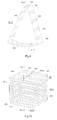
Fig. 4 is a structural schematic diagram of a semiconductor detector provided by an embodiment 3 of the invention; -
Fig. 5 is a structural schematic diagram of a semiconductor detector provided by an embodiment 4 of the invention; -
Fig. 6 is a structural schematic diagram of a semiconductor detector provided by an embodiment 5 of the invention; -
Fig. 7 is a structural schematic diagram of a semiconductor detector provided by an embodiment 6 of the invention; -
Fig. 8 is a structural schematic diagram of a semiconductor detector provided by an embodiment 7 of the invention; -
Fig. 9 is a structural schematic diagram of a semiconductor detector provided by an embodiment 8 of the invention; -
Fig. 10 is a structural schematic diagram of a semiconductor detector provided by an embodiment 9 of the invention; -
Fig. 11 is a structural schematic diagram of a semiconductor detector provided by an embodiment 10 of the invention; -
Fig. 12 is a structural schematic diagram of a semiconductor detector provided by an embodiment 11 of the invention; and -
Fig. 13 is a structural schematic diagram of a semiconductor detector provided by an embodiment 12 of the invention. - The inventive content of the invention will be further described in detail in the following with reference to the drawings and embodiments.
- As shown in
Fig. 1 , asemiconductor detector 100 provided by this embodiment comprises asemiconductor crystal 101, acathode 102, ananode 103, afirst ladder electrode 104 and asecond ladder electrode 105. - In this embodiment, the shape of the
semiconductor crystal 101 is a cuboid. The material of thesemiconductor crystal 101 comprises HgI2, GaAs, TiBr, CdTe, CdZnTe, CdSe, GaP, HgS, PbI2, or AlSb. - In this embodiment, the
cathode 102, theanode 103, thefirst ladder electrode 104 and thesecond ladder electrode 105 are conductive thin films deposited on a surface of thesemiconductor crystal 101. The material of thecathode 102, theanode 103, thefirst ladder electrode 104 and thesecond ladder electrode 105 comprises Au, Pt, Ag, Cu, Al or ITO. Thecathode 102 is disposed on a bottom surface 101-1 of thesemiconductor crystal 101, and covers the full area of the bottom surface 101-1 of thesemiconductor crystal 101. Theanode 103 is disposed on a top surface 101-2 of thesemiconductor crystal 101, and covers a partial area at a middle position of the top surface 101-2. Preferably, theanode 103 is rectangular, the two relatively short sides of theanode 103 coincide with the two relatively long sides of the top surface 101-2 respectively, namely, the long sides of theanode 103 are equal to the short sides of the top surface 101-2; the two relatively long sides of theanode 103 are parallel to the two relatively short sides of the top surface 101-2. - In this embodiment, the
first ladder electrode 104 is disposed on a first side 101-3 of thesemiconductor crystal 101, thesecond ladder electrode 105 is disposed on a second side 101-4 of thesemiconductor crystal 101, and the positions of the first side 101-3 and the second side 101-4 are opposite to each other. Thefirst ladder electrode 104 comprises a plurality of rectangular sub-electrodes disposed on the first side 101-3, and a gap is disposed between any two adjacent sub-electrodes thereof. Thesecond ladder electrode 105 is disposed on the second side 101-4 of thesemiconductor crystal 101, and a gap is disposed between any two adjacent sub-electrodes thereof. The individual sub-electrodes of thefirst ladder electrode 104 may be non-uniformly disposed on the first side 101-3. The individual sub-electrodes of thesecond ladder electrode 105 may be non-uniformly disposed on the second side 101-4. Preferably, the individual sub-electrodes of thefirst ladder electrode 104 are uniformly disposed on the first side 101-3. The individual sub-electrodes of thesecond ladder electrode 105 are uniformly disposed on the second side 101-4. The width of the individual sub-electrodes of thefirst ladder electrode 104 may be different. The width of the individual sub-electrodes of thesecond ladder electrode 105 may be different. Preferably, the width of the individual sub-electrodes of thefirst ladder electrode 104 is identical. The width of the individual sub-electrodes of thesecond ladder electrode 105 is identical. The number and shape of the sub-electrodes of thesecond ladder electrode 105 may be different from those of the sub-electrodes of thefirst ladder electrode 104. Preferably, the number and shape of the sub-electrodes of thesecond ladder electrode 105 are the same as those of the sub-electrodes of thefirst ladder electrode 104, and the positions of the sub-electrodes of thesecond ladder electrode 105 are opposite one by one to those of the sub-electrodes of thefirst ladder electrode 104. Preferably, the long sides of the sub-electrodes of thefirst ladder electrode 104 and thesecond ladder electrode 105 are parallel to the long sides of theanode 103. - When the energy spectrum of high energy rays is measured by applying the semiconductor detector of this embodiment, a ladder bias voltage is applied on the
first ladder electrode 104 and thesecond ladder electrode 105. In particular, according to an order from thecathode 102 to theanode 103, the voltages applied on the individual sub-electrodes of thefirst ladder electrode 104 and thesecond ladder electrode 105 rise in turn. Preferably, the voltages applied on any two sub-electrodes with the same height of thefirst ladder electrode 104 and thesecond ladder electrode 105 are equal. - The semiconductor detector provided by this embodiment causes the average electric field intensity inside the
semiconductor crystal 101 to be increased by arranging the two ladder electrodes, the increase of the average electric field intensity causes the carrier drift time to be shortened, and the shortening of the carrier drift time causes the possibility of carriers being trapped to be lowered, thereby causing the improvement of the energy resolution of the semiconductor detector of this embodiment. -
Fig. 2 is an energy spectrum plot obtained by measuring γ rays of 662 KeV employing thesemiconductor detector 100 of this embodiment. FromFig. 2 , it can be seen that a distinct 662 KeV full energy peak appears in the γ energy spectrum of thesemiconductor detector 100 of this embodiment, and the energy resolution thereof is 1.1%@662keV. This sufficiently shows that the energy resolution of thesemiconductor detector 100 of this embodiment is improved evidently as compared to the semiconductor detector in the prior art. - As shown in
Fig. 3 , the differences between thesemiconductor detector 100 provided by this embodiment and the embodiment 1 lie in that thecathode 102 comprises a plurality of rectangular sub-electrodes disposed on the bottom surface 101-1, and a gap is disposed between any two adjacent sub-electrodes thereof, and the long sides of each sub-electrode of thecathode 102 are parallel to the long sides of theanode 103. The individual sub-electrodes of thecathode 102 may be non-uniformly disposed on the bottom surface 101-1. Preferably, the individual sub-electrodes of thecathode 102 are uniformly disposed on the bottom surface 101-1. The width of the individual sub-electrodes of thecathode 102 may be different. Preferably, the width of the individual sub-electrodes of thecathode 102 is identical. The rest is the same as the embodiment 1. - As shown in
Fig. 4 , the differences between thesemiconductor detector 100 provided by this embodiment and the embodiment 1 lie in that thecathode 102 comprises a plurality of rectangular sub-electrodes disposed on the bottom surface 101-1, and a gap is disposed between any two adjacent sub-electrodes thereof, and the long sides of each sub-electrode of thecathode 102 are perpendicular to the long sides of theanode 103. The individual sub-electrodes of thecathode 102 may be non-uniformly disposed on the bottom surface 101-1. Preferably, the individual sub-electrodes of thecathode 102 are uniformly disposed on the bottom surface 101-1. The width of the individual sub-electrodes of thecathode 102 may be different. Preferably, the width of the individual sub-electrodes of thecathode 102 is identical. The rest is the same as the embodiment 1. - As shown in
Fig. 5 , the differences between thesemiconductor detector 100 provided by this embodiment and the embodiment 1 lie in that thefirst ladder electrode 104 is disposed on the first side 101-3 of thesemiconductor crystal 101 and in a partial area of the top surface 101-2 adjacent to the first side 101-3, i.e., partial sub-electrodes of thefirst ladder electrode 104 are disposed on the first side 101-3, and the remaining partial sub-electrodes are disposed in a partial area of the top surface 101-2 adjacent to the first side 101-3; thesecond ladder electrode 105 is disposed on the second side 101-4 of thesemiconductor crystal 101 and in a partial area of the top surface 101-2 adjacent to the second side 101-4, i.e., partial sub-electrodes of thesecond ladder electrode 105 are disposed on the second side 101-4, and the remaining partial sub-electrodes are disposed in a partial area of the top surface 101-2 adjacent to the second side 101-4. The rest is the same as the embodiment 1. - As shown in
Fig. 6 , the differences between thesemiconductor detector 100 provided by this embodiment and the embodiment 1 lie in that thefirst ladder electrode 104 is disposed on the first side 101-3 of thesemiconductor crystal 101 and in a partial area of the top surface 101-2 adjacent to the first side 101-3, i.e., partial sub-electrodes of thefirst ladder electrode 104 are disposed on the first side 101-3, and the remaining partial sub-electrodes are disposed in a partial area of the top surface 101-2 adjacent to the first side 101-3; thesecond ladder electrode 105 is disposed on the second side 101-4 of thesemiconductor crystal 101 and in a partial area of the top surface 101-2 adjacent to the second side 101-4, i.e., partial sub-electrodes of thesecond ladder electrode 105 are disposed on the second side 101-4, and the remaining partial sub-electrodes are disposed in a partial area of the top surface 101-2 adjacent to the second side 101-4; thecathode 102 comprises a plurality of rectangular sub-electrodes disposed on the bottom surface 101-1, and a gap is disposed between any two adjacent sub-electrodes thereof, and the long sides of each sub-electrode of thecathode 102 are parallel to the long sides of theanode 103. The individual sub-electrodes of thecathode 102 may be non-uniformly disposed on the bottom surface 101-1. Preferably, the individual sub-electrodes of thecathode 102 are uniformly disposed on the bottom surface 101-1. The width of the individual sub-electrodes of thecathode 102 may be different. Preferably, the width of the individual sub-electrodes of thecathode 102 is identical. The rest is the same as the embodiment 1. - As shown in
Fig. 7 , the differences between thesemiconductor detector 100 provided by this embodiment and the embodiment 1 lie in that thefirst ladder electrode 104 is disposed on the first side 101-3 of thesemiconductor crystal 101 and in a partial area of the top surface 101-2 adjacent to the first side 101-3, i.e., partial sub-electrodes of thefirst ladder electrode 104 are disposed on the first side 101-3, and the remaining partial sub-electrodes are disposed in a partial area of the top surface 101-2 adjacent to the first side 101-3; thesecond ladder electrode 105 is disposed on the second side 101-4 of thesemiconductor crystal 101 and in a partial area of the top surface 101-2 adjacent to the second side 101-4, i.e., partial sub-electrodes of thesecond ladder electrode 105 are disposed on the second side 101-4, and the remaining partial sub-electrodes are disposed in a partial area of the top surface 101-2 adjacent to the second side 101-4; thecathode 102 comprises a plurality of rectangular sub-electrodes disposed on the bottom surface 101-1, and a gap is disposed between any two adjacent sub-electrodes thereof, and the long sides of each sub-electrode of thecathode 102 are perpendicular to the long sides of theanode 103. The individual sub-electrodes of thecathode 102 may be non-uniformly disposed on the bottom surface 101-1. Preferably, the individual sub-electrodes of thecathode 102 are uniformly disposed on the bottom surface 101-1. The width of the individual sub-electrodes of thecathode 102 may be different. Preferably, the width of the individual sub-electrodes of thecathode 102 is identical. The rest is the same as the embodiment 1. - As shown in
Fig. 8 , the differences between thesemiconductor detector 100 provided by this embodiment and the embodiment 1 lie in that the edges where the bottom surface 101-1 of thesemiconductor crystal 101 joins the first side 101-3 and the second side 101-4 are chamfered, and thecathode 102 covers the full area of the chamfered bottom surface 101-1 of thesemiconductor crystal 101. The rest is the same as the embodiment 1. - As shown in
Fig. 9 , the differences between thesemiconductor detector 100 provided by this embodiment and the embodiment 1 lie in that the profile of thesemiconductor crystal 101 is fan-shaped, its bottom surface 101-1 is an arc-shaped surface, its top surface 101-2 is rectangular, and theanode 103 is disposed on the top surface 101-2 of thesemiconductor crystal 101 and covers the full area of the top surface 101-2. The rest is the same as the embodiment 1. - As shown in
Fig. 10 , the differences between the semiconductor detector 100 provided by this embodiment and the embodiment 1 lie in that the semiconductor detector 100 provided by this embodiment comprises a semiconductor crystal 101, a cathode 102, an anode 103, a first ladder electrode 104, a second ladder electrode 105, a third ladder electrode 106 and a fourth ladder electrode 107; the anode 103 is circular or elliptic; the third ladder electrode 106 is disposed on a third side 101-5 of the semiconductor crystal 101, the fourth ladder electrode 107 is disposed on a fourth side 101-6 of the semiconductor crystal 101, and the positions of the third side 101-5 and the fourth side 101-6 are opposite to each other; the third ladder electrode 106 comprises a plurality of rectangular sub-electrodes uniformly disposed on the third side 101-5, and a gap is disposed between any two adjacent sub-electrodes thereof; the fourth ladder electrode 107 comprises a plurality of sub-electrodes uniformly disposed on the fourth side 101-6, the number and shape of the sub-electrodes of the third ladder electrode 106 and the fourth ladder electrode 107 are the same as those of the sub-electrodes of the first ladder electrode 104, and the positions of the sub-electrodes of the third ladder electrode 106 are opposite one by one to those of the sub-electrodes of the fourth ladder electrode 107; sub-electrodes with the same height of the first ladder electrode 104, the second ladder electrode 105, the third ladder electrode 106 and the fourth ladder electrode 107 are connected with each other to form a loop. The width of the individual sub-electrodes of thefirst ladder electrode 104 may be different. The width of the individual sub-electrodes of thesecond ladder electrode 105 may be different. The width of the individual sub-electrodes of thethird ladder electrode 106 may be different. The width of the individual sub-electrodes of thefourth ladder electrode 107 may be different. Preferably, the width of the individual sub-electrodes of thefirst ladder electrode 104 is identical. The width of the individual sub-electrodes of thesecond ladder electrode 105 is identical. The width of the individual sub-electrodes of thethird ladder electrode 106 is identical. The width of the individual sub-electrodes of thefourth ladder electrode 107 is identical. More preferably, the width of all the sub-electrodes of thefirst ladder electrode 104, thesecond ladder electrode 105, thethird ladder electrode 106 and thefourth ladder electrode 107 is identical. The rest is the same as the embodiment 1. - As shown in
Fig. 11 , the differences between thesemiconductor detector 100 provided by this embodiment and the embodiment 1 lie in that thesemiconductor detector 100 provided by this embodiment comprises asemiconductor crystal 101, acathode 102, ananode 103 and afirst ladder electrode 104; thesemiconductor crystal 101 is cylindrical, theanode 103 is circular or elliptic, and theanode 103 covers a partial area in the middle of the top surface 101-2; thefirst ladder electrode 104 is disposed on a first side 101-3 of thesemiconductor crystal 101; thefirst ladder electrode 104 comprises a plurality of annular sub-electrodes uniformly disposed on the first side 101-3, and a gap is disposed between any two adjacent sub-electrodes thereof. Preferably, the sub-electrodes of thefirst ladder electrode 104 are parallel to the top surface 101-2 of thesemiconductor crystal 101. The width of the individual sub-electrodes of thefirst ladder electrode 104 may be different. Preferably, the width of the individual sub-electrodes of thefirst ladder electrode 104 is identical. The rest is the same as the embodiment 1. - It needs to be noted that, in addition to this embodiment, the
semiconductor crystal 101 may be semi-cylindrical in other preferred embodiments (not shown in the figure). - It needs to be noted that, in addition to this embodiment, the
anode 103 may cover the full area of the top surface 101-2 in other preferred embodiments (not shown in the figure). - It needs to be noted that, in addition to this embodiment, in other preferred embodiments, the
semiconductor detector 100 may comprise afirst ladder electrode 104 and asecond ladder electrode 105, and both thefirst ladder electrode 104 and thesecond ladder electrode 105 comprise a plurality of semi-annular sub-electrodes (not shown in the figure). Preferably, the positions of the sub-electrodes of thefirst ladder electrode 104 are opposite one by one to those of the sub-electrodes of thesecond ladder electrode 105, wherein two sub-electrodes with the same height forms one annulus, and the two sub-electrodes with the same height are provided with an opening at the connection thereof. - As shown in
Fig. 12 , the differences between thesemiconductor detector 100 provided by this embodiment and the embodiment 9 lie in that theanode 103 is rectangular, and theanode 103 covers the full area of the top surface 101-2 of thesemiconductor crystal 101. The rest is the same as the embodiment 9. - As shown in
Fig. 13 , the differences between thesemiconductor detector 100 provided by this embodiment and the embodiment 9 lie in that theanode 103 is rectangular, and theanode 103 covers the full area of the top surface 101-2 of thesemiconductor crystal 101; sub-electrodes with the same height of thefirst ladder electrode 104, thesecond ladder electrode 105, thethird ladder electrode 106 and thefourth ladder electrode 107 are separated from each other, namely, sub-electrodes with the same height of two ladder electrodes disposed on any two adjacent sides of thesemiconductor crystal 101 are provided with openings at the connection of the two sides. The width of the individual sub-electrodes of thefirst ladder electrode 104 may be different. The width of the individual sub-electrodes of thesecond ladder electrode 105 may be different. The width of the individual sub-electrodes of thethird ladder electrode 106 may be different. The width of the individual sub-electrodes of thefourth ladder electrode 107 may be different. Preferably, the width of the individual sub-electrodes of thefirst ladder electrode 104 is identical. The width of the individual sub-electrodes of thesecond ladder electrode 105 is identical. The width of the individual sub-electrodes of thethird ladder electrode 106 is identical. The width of the individual sub-electrodes of thefourth ladder electrode 107 is identical. More preferably, the width of all the sub-electrodes of thefirst ladder electrode 104, thesecond ladder electrode 105, thethird ladder electrode 106 and thefourth ladder electrode 107 is identical. The rest is the same as the embodiment 9. - The above embodiments are used only to illustrate the invention and not to limit the invention, and also various variations and modifications may be made by those of ordinary skills in the related art without departing from the spirit and scope of the invention, therefore, all equivalent technical solutions also pertain to the category of the invention. The patent protection scope should be defined by the claims.
Claims (24)
- A semiconductor detector, characterized in that, the semiconductor detector comprises a semiconductor crystal, a cathode, an anode and at least one ladder electrode;
the semiconductor crystal comprises a top surface, a bottom surface and at least one side; the cathode, the anode and the ladder electrode are conductive thin films deposited on a surface of the semiconductor crystal;
the cathode is disposed on the bottom surface of the semiconductor crystal, the anode is disposed on the top surface of the semiconductor crystal, and the ladder electrode is disposed on the at least one side of the semiconductor crystal; and
the ladder electrode comprises a plurality of sub-electrodes. - The semiconductor detector as claimed in claim 1, characterized in that, the shape of the semiconductor crystal is a cuboid.
- The semiconductor detector as claimed in claim 2, characterized in that, the anode is rectangular and covers a partial area at a middle position of the top surface; the semiconductor detector comprises a first ladder electrode and a second ladder electrode; the first ladder electrode and the second ladder electrode are disposed respectively on a first side and a second side of the semiconductor crystal with their positions being opposite.
- The semiconductor detector as claimed in claim 3, characterized in that, the cathode covers the full area of the bottom surface.
- The semiconductor detector as claimed in claim 3, characterized in that, the cathode comprises a plurality of rectangular sub-electrodes uniformly disposed on the bottom surface, and a gap is disposed between any two adjacent sub-electrodes thereof.
- The semiconductor detector as claimed in claim 5, characterized in that, the long sides of a sub-electrode of the cathode are parallel to the long sides of the anode.
- The semiconductor detector as claimed in claim 5, characterized in that, the long sides of a sub-electrode of the cathode are perpendicular to the long sides of the anode.
- The semiconductor detector as claimed in any of claims 3-7, characterized in that, the first ladder electrode comprises a plurality of rectangular sub-electrodes uniformly disposed on the first side, and a gap is disposed between any two adjacent sub-electrodes thereof; the second ladder electrode comprises a plurality of sub-electrodes uniformly disposed on the second side, the number and shape of the sub-electrodes of the second ladder electrode are the same as those of the sub-electrodes of the first ladder electrode, and the positions of the sub-electrodes of the second ladder electrode are opposite one by one to those of the sub-electrodes of the first ladder electrode.
- The semiconductor detector as claimed in any of claims 3-7, characterized in that, the first ladder electrode comprises a plurality of rectangular sub-electrodes uniformly disposed on the first side and in a partial area of the top surface adjacent to the first side, and a gap is disposed between any two adjacent sub-electrodes thereof; the second ladder electrode comprises a plurality of sub-electrodes uniformly disposed on the second side and in a partial area of the top surface adjacent to the second side, the number and shape of the sub-electrodes of the second ladder electrode are the same as those of the sub-electrodes of the first ladder electrode, and the positions of the sub-electrodes of the second ladder electrode are opposite one by one to those of the sub-electrodes of the first ladder electrode.
- The semiconductor detector as claimed in claim 3, characterized in that, the edges where the bottom surface of the semiconductor crystal joins the first side and the second side are chamfered, and the cathode covers the full area of the chamfered bottom surface of the semiconductor crystal.
- The semiconductor detector as claimed in claim 10, characterized in that, the first ladder electrode comprises a plurality of rectangular sub-electrodes uniformly disposed on the first side, and a gap is disposed between any two adjacent sub-electrodes thereof; the second ladder electrode comprises a plurality of sub-electrodes uniformly disposed on the second side, the number and shape of the sub-electrodes of the second ladder electrode are the same as those of the sub-electrodes of the first ladder electrode, and the positions of the sub-electrodes of the second ladder electrode are opposite one by one to those of the sub-electrodes of the first ladder electrode.
- The semiconductor detector as claimed in claim 1, characterized in that, the profile of the semiconductor crystal is fan-shaped, the bottom surface is an arc-shaped surface, the top surface is rectangular, and the anode is disposed on the top surface and covers the full area of the top surface.
- The semiconductor detector as claimed in claim 12, characterized in that, the semiconductor detector comprises a first ladder electrode and a second ladder electrode; and the first ladder electrode and the second ladder electrode are disposed respectively on a first side and a second side of the semiconductor crystal with their positions being opposite.
- The semiconductor detector as claimed in claim 13, characterized in that, the first ladder electrode comprises a plurality of rectangular sub-electrodes uniformly disposed on the first side, and a gap is disposed between any two adjacent sub-electrodes thereof; the second ladder electrode comprises a plurality of sub-electrodes uniformly disposed on the second side, the number and shape of the sub-electrodes of the second ladder electrode are the same as those of the sub-electrodes of the first ladder electrode, and the positions of the sub-electrodes of the second ladder electrode are opposite one by one to those of the sub-electrodes of the first ladder electrode.
- The semiconductor detector as claimed in claim 2, characterized in that, the anode is circular or elliptic and covers a partial area at a middle position of the top surface; the cathode covers the full area of the bottom surface; the semiconductor detector comprises a first ladder electrode, a second ladder electrode, a third ladder electrode, and a fourth ladder electrode; the first ladder electrode and the second ladder electrode are disposed respectively on a first side and a second side of the semiconductor crystal with their positions being opposite, and the third ladder electrode and the fourth ladder electrode are disposed respectively on a third side and a fourth side of the semiconductor crystal with their positions being opposite.
- The semiconductor detector as claimed in claim 15, characterized in that, the first ladder electrode comprises a plurality of rectangular sub-electrodes uniformly disposed on the first side, and a gap is disposed between any two adjacent sub-electrodes thereof; the second ladder electrode, the third ladder electrode and the fourth ladder electrode in turn comprise a plurality of sub-electrodes uniformly disposed on the second side, the third side and the fourth side respectively, the number and shape of the sub-electrodes of the second ladder electrode, the third ladder electrode and the fourth ladder electrode are the same as those of the sub-electrodes of the first ladder electrode, and the positions of the sub-electrodes of the second ladder electrode are opposite one by one to those of the sub-electrodes of the first ladder electrode, the positions of the sub-electrodes of the third ladder electrode are opposite one by one to those of the sub-electrodes of the fourth ladder electrode; sub-electrodes with the same height of the first ladder electrode, the second ladder electrode, the third ladder electrode and the fourth ladder electrode are connected with each other to form a loop.
- The semiconductor detector as claimed in claim 1, characterized in that, the shape of the semiconductor crystal is a cylinder.
- The semiconductor detector as claimed in claim 17, characterized in that, the anode is circular or elliptic and covers a partial area at a middle position of the top surface; the cathode covers the full area of the bottom surface; the semiconductor detector comprises a first ladder electrode; and the first ladder electrode is disposed on a first side of the semiconductor crystal.
- The semiconductor detector as claimed in claim 18, characterized in that, the first ladder electrode comprises a plurality of annular sub-electrodes uniformly disposed on the first side, and a gap is disposed between any two adjacent sub-electrodes thereof; the sub-electrodes of the first ladder electrode are parallel to the top surface.
- The semiconductor detector as claimed in claim 2, characterized in that, the anode is rectangular and covers the full area of the top surface; the cathode covers the full area of the bottom surface; the semiconductor detector comprises a first ladder electrode, a second ladder electrode, a third ladder electrode, and a fourth ladder electrode; the first ladder electrode and the second ladder electrode are disposed respectively on a first side and a second side of the semiconductor crystal with their positions being opposite, and the third ladder electrode and the fourth ladder electrode are disposed respectively on a third side and a fourth side of the semiconductor crystal with their positions being opposite.
- The semiconductor detector as claimed in claim 20, characterized in that, the first ladder electrode comprises a plurality of rectangular sub-electrodes uniformly disposed on the first side, and a gap is disposed between any two adjacent sub-electrodes thereof; the second ladder electrode, the third ladder electrode and the fourth ladder electrode in turn comprise a plurality of sub-electrodes uniformly disposed on the second side, the third side and the fourth side respectively, the number and shape of the sub-electrodes of the second ladder electrode, the third ladder electrode and the fourth ladder electrode are the same as those of the sub-electrodes of the first ladder electrode, and the positions of the sub-electrodes of the second ladder electrode are opposite one by one to those of the sub-electrodes of the first ladder electrode, the positions of the sub-electrodes of the third ladder electrode are opposite one by one to those of the sub-electrodes of the fourth ladder electrode; sub-electrodes with the same height of the first ladder electrode, the second ladder electrode, the third ladder electrode and the fourth ladder electrode are connected with each other to form a loop.
- The semiconductor detector as claimed in claim 20, characterized in that, the first ladder electrode comprises a plurality of rectangular sub-electrodes uniformly disposed on the first side, and a gap is disposed between any two adjacent sub-electrodes thereof; the second ladder electrode, the third ladder electrode and the fourth ladder electrode in turn comprise a plurality of sub-electrodes uniformly disposed on the second side, the third side and the fourth side respectively, the number and shape of the sub-electrodes of the second ladder electrode, the third ladder electrode and the fourth ladder electrode are the same as those of the sub-electrodes of the first ladder electrode, and the positions of the sub-electrodes of the second ladder electrode are opposite one by one to those of the sub-electrodes of the first ladder electrode, the positions of the sub-electrodes of the third ladder electrode are opposite one by one to those of the sub-electrodes of the fourth ladder electrode; sub-electrodes with the same height of two of the ladder electrodes disposed on any two adjacent ones of the sides of the semiconductor crystal are provided with openings at the connection of the two sides.
- The semiconductor detector as claimed in any of claims 1-22, characterized in that, the material of the semiconductor crystal comprises HgI2, GaAs, TiBr, CdTe, CdZnTe, CdSe, GaP, HgS, PbI2, or AlSb.
- The semiconductor detector as claimed in any of claims 1-22, characterized in that, the material of the cathode, the anode and the ladder electrode comprises Au, Pt, Ag, Cu, Al or ITO.
Priority Applications (1)
| Application Number | Priority Date | Filing Date | Title |
|---|---|---|---|
| PL14150977T PL2796897T3 (en) | 2013-04-26 | 2014-01-13 | Semiconductor detector |
Applications Claiming Priority (2)
| Application Number | Priority Date | Filing Date | Title |
|---|---|---|---|
| CN 201320218487 CN203204163U (en) | 2013-04-26 | 2013-04-26 | Semiconductor detector |
| CN2013101493976A CN103235332A (en) | 2013-04-26 | 2013-04-26 | Semiconductor detector |
Publications (2)
| Publication Number | Publication Date |
|---|---|
| EP2796897A1 true EP2796897A1 (en) | 2014-10-29 |
| EP2796897B1 EP2796897B1 (en) | 2019-04-17 |
Family
ID=49989516
Family Applications (1)
| Application Number | Title | Priority Date | Filing Date |
|---|---|---|---|
| EP14150977.8A Active EP2796897B1 (en) | 2013-04-26 | 2014-01-13 | Semiconductor detector |
Country Status (4)
| Country | Link |
|---|---|
| US (1) | US9766354B2 (en) |
| EP (1) | EP2796897B1 (en) |
| PL (1) | PL2796897T3 (en) |
| WO (1) | WO2014172822A1 (en) |
Cited By (2)
| Publication number | Priority date | Publication date | Assignee | Title |
|---|---|---|---|---|
| DE102016203861A1 (en) * | 2016-03-09 | 2017-09-14 | Siemens Healthcare Gmbh | Converter element with guide element |
| CN118839582A (en) * | 2024-06-25 | 2024-10-25 | 西安中核核仪器股份有限公司 | High-precision characterization method of rounded high-purity germanium detector |
Families Citing this family (2)
| Publication number | Priority date | Publication date | Assignee | Title |
|---|---|---|---|---|
| US9618633B2 (en) * | 2015-04-21 | 2017-04-11 | Toshiba Medical Systems Corporation | Side-electrodes for a Faraday cage on a photon-counting detector array |
| DE102015116270B4 (en) | 2015-09-25 | 2018-02-15 | Deutsches Elektronen-Synchrotron Desy | Sensor for the detection of charged particles and photons |
Citations (3)
| Publication number | Priority date | Publication date | Assignee | Title |
|---|---|---|---|---|
| US6037595A (en) * | 1995-10-13 | 2000-03-14 | Digirad Corporation | Radiation detector with shielding electrode |
| US6175120B1 (en) * | 1998-05-08 | 2001-01-16 | The Regents Of The University Of Michigan | High-resolution ionization detector and array of such detectors |
| EP1351309A2 (en) * | 2002-04-02 | 2003-10-08 | Hitachi, Ltd. | Radiation detector and radiation apparatus |
Family Cites Families (12)
| Publication number | Priority date | Publication date | Assignee | Title |
|---|---|---|---|---|
| GB1559664A (en) * | 1977-02-17 | 1980-01-23 | Tokyo Shibaura Electric Co | Semiconductor radiation detector |
| IL119075A (en) * | 1996-08-14 | 1999-11-30 | Imarad Imaging Systems Ltd | Semiconductor detector |
| US6069360A (en) * | 1998-05-08 | 2000-05-30 | Lund; James C. | Method and apparatus for electron-only radiation detectors from semiconductor materials |
| US7589324B2 (en) | 2006-12-21 | 2009-09-15 | Redlen Technologies | Use of solder mask as a protective coating for radiation detector |
| US8183531B2 (en) * | 2007-05-21 | 2012-05-22 | The Board Of Trustees Of The Leland Stanford Junior University | System and method for tomography combining single and paired photons |
| CN101576516B (en) * | 2008-05-09 | 2011-12-21 | 同方威视技术股份有限公司 | Gas radiation detector and radiation imaging system |
| CN101577284B (en) | 2008-05-09 | 2011-04-13 | 同方威视技术股份有限公司 | Semiconductor detector for measuring radiation and imaging device |
| JP5155808B2 (en) * | 2008-10-08 | 2013-03-06 | 株式会社日立製作所 | Semiconductor radiation detector and nuclear medicine diagnostic equipment |
| US20100252744A1 (en) | 2009-04-06 | 2010-10-07 | Koninklijke Philips Electronics N.V. | Radiation detector with a plurality of electrode systems |
| US20110108703A1 (en) | 2009-11-10 | 2011-05-12 | Orbotech Medical Solutions Ltd. | Segmented guard strip |
| CN203204163U (en) | 2013-04-26 | 2013-09-18 | 清华大学 | Semiconductor detector |
| CN103235332A (en) * | 2013-04-26 | 2013-08-07 | 清华大学 | Semiconductor detector |
-
2013
- 2013-12-09 WO PCT/CN2013/001520 patent/WO2014172822A1/en not_active Ceased
-
2014
- 2014-01-10 US US14/152,332 patent/US9766354B2/en active Active
- 2014-01-13 PL PL14150977T patent/PL2796897T3/en unknown
- 2014-01-13 EP EP14150977.8A patent/EP2796897B1/en active Active
Patent Citations (3)
| Publication number | Priority date | Publication date | Assignee | Title |
|---|---|---|---|---|
| US6037595A (en) * | 1995-10-13 | 2000-03-14 | Digirad Corporation | Radiation detector with shielding electrode |
| US6175120B1 (en) * | 1998-05-08 | 2001-01-16 | The Regents Of The University Of Michigan | High-resolution ionization detector and array of such detectors |
| EP1351309A2 (en) * | 2002-04-02 | 2003-10-08 | Hitachi, Ltd. | Radiation detector and radiation apparatus |
Non-Patent Citations (1)
| Title |
|---|
| SHIN-NOSUKE ISHIKAWA ET AL: "Development of Double-Sided CdTe Strip Detectors for ã-Ray Imaging and Spectroscopy", JAPANESE JOURNAL OF APPLIED PHYSICS, JAPAN SOCIETY OF APPLIED PHYSICS, JP, vol. 49, no. 11, 1 November 2010 (2010-11-01), pages 116702 - 1, XP001560477, ISSN: 0021-4922, [retrieved on 20101122], DOI: 10.1143/JJAP.49.116702 * |
Cited By (2)
| Publication number | Priority date | Publication date | Assignee | Title |
|---|---|---|---|---|
| DE102016203861A1 (en) * | 2016-03-09 | 2017-09-14 | Siemens Healthcare Gmbh | Converter element with guide element |
| CN118839582A (en) * | 2024-06-25 | 2024-10-25 | 西安中核核仪器股份有限公司 | High-precision characterization method of rounded high-purity germanium detector |
Also Published As
| Publication number | Publication date |
|---|---|
| EP2796897B1 (en) | 2019-04-17 |
| US20140319635A1 (en) | 2014-10-30 |
| US9766354B2 (en) | 2017-09-19 |
| WO2014172822A1 (en) | 2014-10-30 |
| PL2796897T3 (en) | 2019-12-31 |
Similar Documents
| Publication | Publication Date | Title |
|---|---|---|
| US9287433B2 (en) | Radiation detector | |
| US6333504B1 (en) | Semiconductor radiation detector with enhanced charge collection | |
| US7977643B2 (en) | Radiation detector assembly, radiation detector, and method for radiation detection | |
| US9018589B2 (en) | Direct conversion X-ray detector | |
| US11002864B2 (en) | Depth correction in pixellated detectors of ionizing radiation | |
| CN103913763B (en) | Radiation detector and radiation detector assembly | |
| WO2023066094A1 (en) | γ-RAY DETECTION STRUCTURE BASED ON PEROVSKITE P-I-N JUNCTION, AND CORRECTION METHOD | |
| US9766354B2 (en) | Semiconductor detector | |
| CN105242300A (en) | Signal processing method of semiconductor detector and device | |
| CN103235332A (en) | Semiconductor detector | |
| US9482762B2 (en) | Gamma ray detector and method of detecting gamma rays | |
| CN203204163U (en) | Semiconductor detector | |
| US9608157B2 (en) | Photon counting semiconductor detectors | |
| Du et al. | Temporal response of CZT detectors under intense irradiation | |
| CN203037860U (en) | Radiation detector and radiation detecting apparatus | |
| US9086490B2 (en) | Red boron solid state detector | |
| CN203071113U (en) | Radiation detector | |
| CN105759303B (en) | A kind of semiconductor detector | |
| EP3730972A1 (en) | Radiation detection device for detecting gamma or x-ray radiation quanta | |
| Zha et al. | The analysis of X-ray response of CdZnTe detectors | |
| CN105676264A (en) | Semiconductor detector | |
| Bolotnikov et al. | Array of virtual Frisch-grid detectors with common cathode and reduced length of shielding electrodes | |
| McGregor et al. | Design considerations for trapezoid-shaped Frisch-grid semiconductor radiation detectors | |
| Zhang et al. | Signal processing of a strengthened electric field line anode CdZnTe detector | |
| Toney | Three-Dimensional Simulation of Signal Generation in Wide-Bandgap Semiconductor Radiation Detectors |
Legal Events
| Date | Code | Title | Description |
|---|---|---|---|
| PUAI | Public reference made under article 153(3) epc to a published international application that has entered the european phase |
Free format text: ORIGINAL CODE: 0009012 |
|
| 17P | Request for examination filed |
Effective date: 20140113 |
|
| AK | Designated contracting states |
Kind code of ref document: A1 Designated state(s): AL AT BE BG CH CY CZ DE DK EE ES FI FR GB GR HR HU IE IS IT LI LT LU LV MC MK MT NL NO PL PT RO RS SE SI SK SM TR |
|
| AX | Request for extension of the european patent |
Extension state: BA ME |
|
| R17P | Request for examination filed (corrected) |
Effective date: 20150427 |
|
| RBV | Designated contracting states (corrected) |
Designated state(s): AL AT BE BG CH CY CZ DE DK EE ES FI FR GB GR HR HU IE IS IT LI LT LU LV MC MK MT NL NO PL PT RO RS SE SI SK SM TR |
|
| GRAP | Despatch of communication of intention to grant a patent |
Free format text: ORIGINAL CODE: EPIDOSNIGR1 |
|
| STAA | Information on the status of an ep patent application or granted ep patent |
Free format text: STATUS: GRANT OF PATENT IS INTENDED |
|
| INTG | Intention to grant announced |
Effective date: 20181112 |
|
| GRAS | Grant fee paid |
Free format text: ORIGINAL CODE: EPIDOSNIGR3 |
|
| GRAA | (expected) grant |
Free format text: ORIGINAL CODE: 0009210 |
|
| STAA | Information on the status of an ep patent application or granted ep patent |
Free format text: STATUS: THE PATENT HAS BEEN GRANTED |
|
| AK | Designated contracting states |
Kind code of ref document: B1 Designated state(s): AL AT BE BG CH CY CZ DE DK EE ES FI FR GB GR HR HU IE IS IT LI LT LU LV MC MK MT NL NO PL PT RO RS SE SI SK SM TR |
|
| REG | Reference to a national code |
Ref country code: GB Ref legal event code: FG4D |
|
| REG | Reference to a national code |
Ref country code: CH Ref legal event code: EP |
|
| REG | Reference to a national code |
Ref country code: DE Ref legal event code: R096 Ref document number: 602014044759 Country of ref document: DE |
|
| REG | Reference to a national code |
Ref country code: AT Ref legal event code: REF Ref document number: 1122190 Country of ref document: AT Kind code of ref document: T Effective date: 20190515 Ref country code: IE Ref legal event code: FG4D |
|
| REG | Reference to a national code |
Ref country code: NL Ref legal event code: FP |
|
| REG | Reference to a national code |
Ref country code: LT Ref legal event code: MG4D |
|
| PG25 | Lapsed in a contracting state [announced via postgrant information from national office to epo] |
Ref country code: ES Free format text: LAPSE BECAUSE OF FAILURE TO SUBMIT A TRANSLATION OF THE DESCRIPTION OR TO PAY THE FEE WITHIN THE PRESCRIBED TIME-LIMIT Effective date: 20190417 Ref country code: AL Free format text: LAPSE BECAUSE OF FAILURE TO SUBMIT A TRANSLATION OF THE DESCRIPTION OR TO PAY THE FEE WITHIN THE PRESCRIBED TIME-LIMIT Effective date: 20190417 Ref country code: PT Free format text: LAPSE BECAUSE OF FAILURE TO SUBMIT A TRANSLATION OF THE DESCRIPTION OR TO PAY THE FEE WITHIN THE PRESCRIBED TIME-LIMIT Effective date: 20190817 Ref country code: SE Free format text: LAPSE BECAUSE OF FAILURE TO SUBMIT A TRANSLATION OF THE DESCRIPTION OR TO PAY THE FEE WITHIN THE PRESCRIBED TIME-LIMIT Effective date: 20190417 Ref country code: LT Free format text: LAPSE BECAUSE OF FAILURE TO SUBMIT A TRANSLATION OF THE DESCRIPTION OR TO PAY THE FEE WITHIN THE PRESCRIBED TIME-LIMIT Effective date: 20190417 Ref country code: HR Free format text: LAPSE BECAUSE OF FAILURE TO SUBMIT A TRANSLATION OF THE DESCRIPTION OR TO PAY THE FEE WITHIN THE PRESCRIBED TIME-LIMIT Effective date: 20190417 Ref country code: FI Free format text: LAPSE BECAUSE OF FAILURE TO SUBMIT A TRANSLATION OF THE DESCRIPTION OR TO PAY THE FEE WITHIN THE PRESCRIBED TIME-LIMIT Effective date: 20190417 Ref country code: NO Free format text: LAPSE BECAUSE OF FAILURE TO SUBMIT A TRANSLATION OF THE DESCRIPTION OR TO PAY THE FEE WITHIN THE PRESCRIBED TIME-LIMIT Effective date: 20190717 |
|
| PG25 | Lapsed in a contracting state [announced via postgrant information from national office to epo] |
Ref country code: RS Free format text: LAPSE BECAUSE OF FAILURE TO SUBMIT A TRANSLATION OF THE DESCRIPTION OR TO PAY THE FEE WITHIN THE PRESCRIBED TIME-LIMIT Effective date: 20190417 Ref country code: GR Free format text: LAPSE BECAUSE OF FAILURE TO SUBMIT A TRANSLATION OF THE DESCRIPTION OR TO PAY THE FEE WITHIN THE PRESCRIBED TIME-LIMIT Effective date: 20190718 Ref country code: LV Free format text: LAPSE BECAUSE OF FAILURE TO SUBMIT A TRANSLATION OF THE DESCRIPTION OR TO PAY THE FEE WITHIN THE PRESCRIBED TIME-LIMIT Effective date: 20190417 Ref country code: BG Free format text: LAPSE BECAUSE OF FAILURE TO SUBMIT A TRANSLATION OF THE DESCRIPTION OR TO PAY THE FEE WITHIN THE PRESCRIBED TIME-LIMIT Effective date: 20190717 |
|
| REG | Reference to a national code |
Ref country code: AT Ref legal event code: MK05 Ref document number: 1122190 Country of ref document: AT Kind code of ref document: T Effective date: 20190417 |
|
| PG25 | Lapsed in a contracting state [announced via postgrant information from national office to epo] |
Ref country code: IS Free format text: LAPSE BECAUSE OF FAILURE TO SUBMIT A TRANSLATION OF THE DESCRIPTION OR TO PAY THE FEE WITHIN THE PRESCRIBED TIME-LIMIT Effective date: 20190817 |
|
| REG | Reference to a national code |
Ref country code: DE Ref legal event code: R097 Ref document number: 602014044759 Country of ref document: DE |
|
| PG25 | Lapsed in a contracting state [announced via postgrant information from national office to epo] |
Ref country code: AT Free format text: LAPSE BECAUSE OF FAILURE TO SUBMIT A TRANSLATION OF THE DESCRIPTION OR TO PAY THE FEE WITHIN THE PRESCRIBED TIME-LIMIT Effective date: 20190417 Ref country code: DK Free format text: LAPSE BECAUSE OF FAILURE TO SUBMIT A TRANSLATION OF THE DESCRIPTION OR TO PAY THE FEE WITHIN THE PRESCRIBED TIME-LIMIT Effective date: 20190417 Ref country code: SK Free format text: LAPSE BECAUSE OF FAILURE TO SUBMIT A TRANSLATION OF THE DESCRIPTION OR TO PAY THE FEE WITHIN THE PRESCRIBED TIME-LIMIT Effective date: 20190417 Ref country code: RO Free format text: LAPSE BECAUSE OF FAILURE TO SUBMIT A TRANSLATION OF THE DESCRIPTION OR TO PAY THE FEE WITHIN THE PRESCRIBED TIME-LIMIT Effective date: 20190417 Ref country code: CZ Free format text: LAPSE BECAUSE OF FAILURE TO SUBMIT A TRANSLATION OF THE DESCRIPTION OR TO PAY THE FEE WITHIN THE PRESCRIBED TIME-LIMIT Effective date: 20190417 Ref country code: EE Free format text: LAPSE BECAUSE OF FAILURE TO SUBMIT A TRANSLATION OF THE DESCRIPTION OR TO PAY THE FEE WITHIN THE PRESCRIBED TIME-LIMIT Effective date: 20190417 |
|
| PLBE | No opposition filed within time limit |
Free format text: ORIGINAL CODE: 0009261 |
|
| STAA | Information on the status of an ep patent application or granted ep patent |
Free format text: STATUS: NO OPPOSITION FILED WITHIN TIME LIMIT |
|
| PG25 | Lapsed in a contracting state [announced via postgrant information from national office to epo] |
Ref country code: SM Free format text: LAPSE BECAUSE OF FAILURE TO SUBMIT A TRANSLATION OF THE DESCRIPTION OR TO PAY THE FEE WITHIN THE PRESCRIBED TIME-LIMIT Effective date: 20190417 Ref country code: IT Free format text: LAPSE BECAUSE OF FAILURE TO SUBMIT A TRANSLATION OF THE DESCRIPTION OR TO PAY THE FEE WITHIN THE PRESCRIBED TIME-LIMIT Effective date: 20190417 |
|
| 26N | No opposition filed |
Effective date: 20200120 |
|
| PG25 | Lapsed in a contracting state [announced via postgrant information from national office to epo] |
Ref country code: TR Free format text: LAPSE BECAUSE OF FAILURE TO SUBMIT A TRANSLATION OF THE DESCRIPTION OR TO PAY THE FEE WITHIN THE PRESCRIBED TIME-LIMIT Effective date: 20190417 |
|
| PG25 | Lapsed in a contracting state [announced via postgrant information from national office to epo] |
Ref country code: SI Free format text: LAPSE BECAUSE OF FAILURE TO SUBMIT A TRANSLATION OF THE DESCRIPTION OR TO PAY THE FEE WITHIN THE PRESCRIBED TIME-LIMIT Effective date: 20190417 |
|
| PG25 | Lapsed in a contracting state [announced via postgrant information from national office to epo] |
Ref country code: MC Free format text: LAPSE BECAUSE OF FAILURE TO SUBMIT A TRANSLATION OF THE DESCRIPTION OR TO PAY THE FEE WITHIN THE PRESCRIBED TIME-LIMIT Effective date: 20190417 |
|
| REG | Reference to a national code |
Ref country code: CH Ref legal event code: PL |
|
| REG | Reference to a national code |
Ref country code: BE Ref legal event code: MM Effective date: 20200131 |
|
| PG25 | Lapsed in a contracting state [announced via postgrant information from national office to epo] |
Ref country code: LU Free format text: LAPSE BECAUSE OF NON-PAYMENT OF DUE FEES Effective date: 20200113 |
|
| PG25 | Lapsed in a contracting state [announced via postgrant information from national office to epo] |
Ref country code: LI Free format text: LAPSE BECAUSE OF NON-PAYMENT OF DUE FEES Effective date: 20200131 Ref country code: CH Free format text: LAPSE BECAUSE OF NON-PAYMENT OF DUE FEES Effective date: 20200131 Ref country code: BE Free format text: LAPSE BECAUSE OF NON-PAYMENT OF DUE FEES Effective date: 20200131 |
|
| PG25 | Lapsed in a contracting state [announced via postgrant information from national office to epo] |
Ref country code: IE Free format text: LAPSE BECAUSE OF NON-PAYMENT OF DUE FEES Effective date: 20200113 |
|
| PG25 | Lapsed in a contracting state [announced via postgrant information from national office to epo] |
Ref country code: MT Free format text: LAPSE BECAUSE OF FAILURE TO SUBMIT A TRANSLATION OF THE DESCRIPTION OR TO PAY THE FEE WITHIN THE PRESCRIBED TIME-LIMIT Effective date: 20190417 Ref country code: CY Free format text: LAPSE BECAUSE OF FAILURE TO SUBMIT A TRANSLATION OF THE DESCRIPTION OR TO PAY THE FEE WITHIN THE PRESCRIBED TIME-LIMIT Effective date: 20190417 |
|
| PG25 | Lapsed in a contracting state [announced via postgrant information from national office to epo] |
Ref country code: MK Free format text: LAPSE BECAUSE OF FAILURE TO SUBMIT A TRANSLATION OF THE DESCRIPTION OR TO PAY THE FEE WITHIN THE PRESCRIBED TIME-LIMIT Effective date: 20190417 |
|
| P01 | Opt-out of the competence of the unified patent court (upc) registered |
Effective date: 20230527 |
|
| PGFP | Annual fee paid to national office [announced via postgrant information from national office to epo] |
Ref country code: NL Payment date: 20260119 Year of fee payment: 13 |
|
| PGFP | Annual fee paid to national office [announced via postgrant information from national office to epo] |
Ref country code: GB Payment date: 20260120 Year of fee payment: 13 |
|
| PGFP | Annual fee paid to national office [announced via postgrant information from national office to epo] |
Ref country code: DE Payment date: 20260128 Year of fee payment: 13 |
|
| PGFP | Annual fee paid to national office [announced via postgrant information from national office to epo] |
Ref country code: FR Payment date: 20260119 Year of fee payment: 13 |
|
| PGFP | Annual fee paid to national office [announced via postgrant information from national office to epo] |
Ref country code: PL Payment date: 20260107 Year of fee payment: 13 |