EP2796209A2 - Capacitive transducer and method of manufacturing the same - Google Patents
Capacitive transducer and method of manufacturing the same Download PDFInfo
- Publication number
- EP2796209A2 EP2796209A2 EP20140163663 EP14163663A EP2796209A2 EP 2796209 A2 EP2796209 A2 EP 2796209A2 EP 20140163663 EP20140163663 EP 20140163663 EP 14163663 A EP14163663 A EP 14163663A EP 2796209 A2 EP2796209 A2 EP 2796209A2
- Authority
- EP
- European Patent Office
- Prior art keywords
- cells
- electrode
- capacitive transducer
- membrane
- vibrating membrane
- Prior art date
- Legal status (The legal status is an assumption and is not a legal conclusion. Google has not performed a legal analysis and makes no representation as to the accuracy of the status listed.)
- Granted
Links
- 238000004519 manufacturing process Methods 0.000 title claims description 13
- 239000012528 membrane Substances 0.000 claims abstract description 85
- 230000005540 biological transmission Effects 0.000 claims description 26
- 238000012545 processing Methods 0.000 claims description 13
- 239000000523 sample Substances 0.000 claims description 13
- 238000000034 method Methods 0.000 claims description 7
- 230000000644 propagated effect Effects 0.000 claims description 3
- 230000015572 biosynthetic process Effects 0.000 claims 1
- 238000002604 ultrasonography Methods 0.000 description 37
- 238000005530 etching Methods 0.000 description 23
- 230000035945 sensitivity Effects 0.000 description 20
- 230000003746 surface roughness Effects 0.000 description 18
- 239000000758 substrate Substances 0.000 description 16
- 238000007789 sealing Methods 0.000 description 14
- 238000000605 extraction Methods 0.000 description 11
- 239000000463 material Substances 0.000 description 8
- 230000006866 deterioration Effects 0.000 description 6
- 239000007788 liquid Substances 0.000 description 6
- 230000005855 radiation Effects 0.000 description 6
- 229910052581 Si3N4 Inorganic materials 0.000 description 5
- 238000006243 chemical reaction Methods 0.000 description 5
- 230000010365 information processing Effects 0.000 description 5
- HQVNEWCFYHHQES-UHFFFAOYSA-N silicon nitride Chemical compound N12[Si]34N5[Si]62N3[Si]51N64 HQVNEWCFYHHQES-UHFFFAOYSA-N 0.000 description 5
- VYPSYNLAJGMNEJ-UHFFFAOYSA-N Silicium dioxide Chemical compound O=[Si]=O VYPSYNLAJGMNEJ-UHFFFAOYSA-N 0.000 description 4
- XAGFODPZIPBFFR-UHFFFAOYSA-N aluminium Chemical compound [Al] XAGFODPZIPBFFR-UHFFFAOYSA-N 0.000 description 4
- 229910052782 aluminium Inorganic materials 0.000 description 4
- 238000002360 preparation method Methods 0.000 description 4
- 229910052814 silicon oxide Inorganic materials 0.000 description 4
- 238000009826 distribution Methods 0.000 description 3
- 229920002120 photoresistant polymer Polymers 0.000 description 3
- 238000000623 plasma-assisted chemical vapour deposition Methods 0.000 description 3
- 239000004065 semiconductor Substances 0.000 description 3
- XUIMIQQOPSSXEZ-UHFFFAOYSA-N Silicon Chemical compound [Si] XUIMIQQOPSSXEZ-UHFFFAOYSA-N 0.000 description 2
- RTAQQCXQSZGOHL-UHFFFAOYSA-N Titanium Chemical compound [Ti] RTAQQCXQSZGOHL-UHFFFAOYSA-N 0.000 description 2
- 239000006096 absorbing agent Substances 0.000 description 2
- 210000000481 breast Anatomy 0.000 description 2
- 239000004020 conductor Substances 0.000 description 2
- 238000003745 diagnosis Methods 0.000 description 2
- 238000005516 engineering process Methods 0.000 description 2
- 238000005259 measurement Methods 0.000 description 2
- 229910052710 silicon Inorganic materials 0.000 description 2
- 239000010703 silicon Substances 0.000 description 2
- 229910052719 titanium Inorganic materials 0.000 description 2
- 239000010936 titanium Substances 0.000 description 2
- VYZAMTAEIAYCRO-UHFFFAOYSA-N Chromium Chemical compound [Cr] VYZAMTAEIAYCRO-UHFFFAOYSA-N 0.000 description 1
- 229910000676 Si alloy Inorganic materials 0.000 description 1
- 238000010521 absorption reaction Methods 0.000 description 1
- CSDREXVUYHZDNP-UHFFFAOYSA-N alumanylidynesilicon Chemical compound [Al].[Si] CSDREXVUYHZDNP-UHFFFAOYSA-N 0.000 description 1
- 230000003321 amplification Effects 0.000 description 1
- 238000004458 analytical method Methods 0.000 description 1
- 230000015556 catabolic process Effects 0.000 description 1
- 230000008859 change Effects 0.000 description 1
- 229910052804 chromium Inorganic materials 0.000 description 1
- 239000011651 chromium Substances 0.000 description 1
- 230000007423 decrease Effects 0.000 description 1
- 238000013461 design Methods 0.000 description 1
- 238000010586 diagram Methods 0.000 description 1
- 239000011521 glass Substances 0.000 description 1
- 239000011810 insulating material Substances 0.000 description 1
- 238000009413 insulation Methods 0.000 description 1
- 239000012212 insulator Substances 0.000 description 1
- 238000000691 measurement method Methods 0.000 description 1
- 238000005459 micromachining Methods 0.000 description 1
- 238000012986 modification Methods 0.000 description 1
- 230000004048 modification Effects 0.000 description 1
- 238000003199 nucleic acid amplification method Methods 0.000 description 1
- 230000003287 optical effect Effects 0.000 description 1
- 230000003647 oxidation Effects 0.000 description 1
- 238000007254 oxidation reaction Methods 0.000 description 1
- 238000010895 photoacoustic effect Methods 0.000 description 1
- 230000009466 transformation Effects 0.000 description 1
Images


Classifications
-
- B—PERFORMING OPERATIONS; TRANSPORTING
- B06—GENERATING OR TRANSMITTING MECHANICAL VIBRATIONS IN GENERAL
- B06B—METHODS OR APPARATUS FOR GENERATING OR TRANSMITTING MECHANICAL VIBRATIONS OF INFRASONIC, SONIC, OR ULTRASONIC FREQUENCY, e.g. FOR PERFORMING MECHANICAL WORK IN GENERAL
- B06B1/00—Methods or apparatus for generating mechanical vibrations of infrasonic, sonic, or ultrasonic frequency
- B06B1/02—Methods or apparatus for generating mechanical vibrations of infrasonic, sonic, or ultrasonic frequency making use of electrical energy
- B06B1/0292—Electrostatic transducers, e.g. electret-type
-
- G—PHYSICS
- G01—MEASURING; TESTING
- G01N—INVESTIGATING OR ANALYSING MATERIALS BY DETERMINING THEIR CHEMICAL OR PHYSICAL PROPERTIES
- G01N29/00—Investigating or analysing materials by the use of ultrasonic, sonic or infrasonic waves; Visualisation of the interior of objects by transmitting ultrasonic or sonic waves through the object
- G01N29/22—Details, e.g. general constructional or apparatus details
- G01N29/24—Probes
- G01N29/2406—Electrostatic or capacitive probes, e.g. electret or cMUT-probes
-
- G—PHYSICS
- G01—MEASURING; TESTING
- G01N—INVESTIGATING OR ANALYSING MATERIALS BY DETERMINING THEIR CHEMICAL OR PHYSICAL PROPERTIES
- G01N29/00—Investigating or analysing materials by the use of ultrasonic, sonic or infrasonic waves; Visualisation of the interior of objects by transmitting ultrasonic or sonic waves through the object
- G01N29/22—Details, e.g. general constructional or apparatus details
- G01N29/24—Probes
- G01N29/2418—Probes using optoacoustic interaction with the material, e.g. laser radiation, photoacoustics
-
- G—PHYSICS
- G01—MEASURING; TESTING
- G01N—INVESTIGATING OR ANALYSING MATERIALS BY DETERMINING THEIR CHEMICAL OR PHYSICAL PROPERTIES
- G01N29/00—Investigating or analysing materials by the use of ultrasonic, sonic or infrasonic waves; Visualisation of the interior of objects by transmitting ultrasonic or sonic waves through the object
- G01N29/34—Generating the ultrasonic, sonic or infrasonic waves, e.g. electronic circuits specially adapted therefor
-
- G—PHYSICS
- G01—MEASURING; TESTING
- G01N—INVESTIGATING OR ANALYSING MATERIALS BY DETERMINING THEIR CHEMICAL OR PHYSICAL PROPERTIES
- G01N2291/00—Indexing codes associated with group G01N29/00
- G01N2291/04—Wave modes and trajectories
- G01N2291/045—External reflections, e.g. on reflectors
-
- G—PHYSICS
- G01—MEASURING; TESTING
- G01N—INVESTIGATING OR ANALYSING MATERIALS BY DETERMINING THEIR CHEMICAL OR PHYSICAL PROPERTIES
- G01N2291/00—Indexing codes associated with group G01N29/00
- G01N2291/10—Number of transducers
- G01N2291/101—Number of transducers one transducer
-
- Y—GENERAL TAGGING OF NEW TECHNOLOGICAL DEVELOPMENTS; GENERAL TAGGING OF CROSS-SECTIONAL TECHNOLOGIES SPANNING OVER SEVERAL SECTIONS OF THE IPC; TECHNICAL SUBJECTS COVERED BY FORMER USPC CROSS-REFERENCE ART COLLECTIONS [XRACs] AND DIGESTS
- Y10—TECHNICAL SUBJECTS COVERED BY FORMER USPC
- Y10T—TECHNICAL SUBJECTS COVERED BY FORMER US CLASSIFICATION
- Y10T29/00—Metal working
- Y10T29/49—Method of mechanical manufacture
- Y10T29/49002—Electrical device making
- Y10T29/49007—Indicating transducer
Definitions
- the present invention relates to a capacitive transducer and a method of manufacturing same.
- micromechanical components manufactured by micromachining technology have been processable in the order of micrometers. Through use thereof, various micro-functional elements have been realized.
- Capacitive transducers using such technology have been studied as a substitute for piezoelectric elements. With such a capacitive transducer, an ultrasound wave can be transmitted and received using vibration of a vibrating membrane, and excellent wideband characteristics particularly in liquid can be obtained easily.
- capacitive transducer including an element in which cells are arranged in a square shape or rectangle shape and the gaps between adjacent cells are uniform (see Japanese Patent Application Laid-open No. 2008-98697 ). Also, there is a capacitive transducer in which the transmission efficiency or receiving sensitivity of a cell in an end portion of an element is lower than the transmission efficiency or receiving sensitivity of a cell in a middle portion of the element (see US Patent No. 8456958 ).
- the radiated sound pressure is uniform in an end portion and a middle portion of the element. Therefore, a side lobe of an ultrasound beam easily occurs.
- the quality of an ultrasound image using the ultrasound beam may deteriorate due to the side lobe.
- the image quality may deteriorate in a similar manner in the case of reception as well.
- the structure is such that the shape of a cell in the end portion of the element and the shape of a cell in the middle portion of the element differ.
- the present invention has been made based on recognition of such a task.
- the present invention is achieved to reduce a side lobe in a capacitive transducer.
- the present invention in its first aspect provides a capacitive transducer as specified in claims 1 to 3, a probe as specified in claim 4 or an object information acquiring apparatus as specified in claims 5 to 7.
- the present invention in its second aspect provides a method of manufacturing a capacitive transducer as specified in claim 8.
- a side lobe in a capacitive transducer can be reduced.
- the present invention has been made for a capacitive transducer for an ultrasound wave and can be applied to an apparatus and an method for transmitting or receiving an ultrasound wave using the transducer. Further, the subject matter of the present invention includes an apparatus utilizing an ultrasound echo technique in which an ultrasound wave is transmitted to an object such as a living body and an echo wave reflected and propagated inside the object is received. By data generation based on the echo wave, characteristic information reflecting the difference in acoustic impedance inside the object can be acquired.
- the capacitive transducer of the present invention can be utilized in receiving, besides an echo wave, a photoacoustic wave generated and propagated by a light absorber inside an object through a photoacoustic effect when the object is irradiated with light from a light source.
- analyzing the photoacoustic wave functional information or optical characteristic information relating to the inside of the object can be acquired.
- Such apparatuses obtain characteristic information by performing analysis with an information processing device after processing by a signal processing unit has been performed with respect to a received echo wave or photoacoustic wave, and therefore can be referred to as object information acquiring apparatus.
- object information acquiring apparatus By displaying the characteristic information as image data in a display unit, internal examination such as a diagnosis is possible.
- the present invention can also be understood as a method of controlling an object information acquiring apparatus, an object information acquiring method, or an acoustic wave measurement method. Further, the present invention can also be understood as a program that realizes such a method with an information processing unit such as a CPU or circuit. The present invention can also be understood as a method of manufacturing a capacitive transducer characteristic to the present invention or a method of manufacturing a probe using the same.
- a probe in which a single or a plurality of elements are arranged is preferable.
- an object for scanning with the probe By holding an object for scanning with the probe, measurement over a wide range is possible. If the object is a breast, it is preferable to use, for example, a plate-shaped member or cup-shaped member for holding.
- An ultrasound wave referred to in the present invention is given as a typical example of an acoustic wave also called a sound wave or elastic wave.
- the wavelength or the like is not limited.
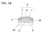
- FIG. 1A is a top view of a capacitive transducer of the present invention
- FIG. 1B is a sectional view along line A-B in FIG. 1A
- an element 14 of the capacitive transducer of the present invention a plurality of cells 12 are formed.
- the number of elements included in the capacitive transducer is one in FIG. 1A , but may any number.
- an element refers to each element of the capacitive transducer of which a signal extraction electrode is shared by all cells forming the element. That is, output of an electrical signal is performed in terms of the elements.
- the number of cells included in the element 14 is sixty three in FIG. 1A , but may be any number.
- a vibrating membrane 9 is supported to be capable of vibration.
- the vibrating membrane 9 includes a second electrode 1.
- the second electrode 1 is provided such that a first electrode 2 is across a gap 3 (i.e., cavity).
- the vibrating membrane has a configuration in which the second electrode 1 is sandwiched between a first membrane 7 and a second membrane 8.
- a configuration with only the second electrode or only the first membrane and the second electrode is acceptable, as long as the vibrating membrane is capable of vibration and includes the second electrode.
- reference numeral 4 denotes an etching path
- reference numeral 6 denotes a sealing portion
- reference numeral 10 denotes a substrate
- reference numerals 11 and 15 denote first and second insulating films.
- the first electrode or the second electrode is used as an electrode for applying bias voltage or an electrode for adding an electrical signal or extracting an electrical signal.
- the first electrode is used as an electrode for applying bias voltage and the second electrode is used as a signal extraction electrode, but it may be the opposite.
- the electrode for applying bias voltage is also shared within an element. The configuration may be such that the bias voltage is shared between elements. However, the signal extraction electrode has to be electrically separated for each element.
- the gap between cells in an end portion of the element is greater than the gap between cells in a middle portion of the element. It is preferable that the gap between the cells become narrower from the end portion toward the middle portion of the element. It suffices that the gap between a pair of cells in the end portion of the element and the gap between a pair of cells in the middle portion of the element be designed depending on the shape of an intended ultrasound beam. For example, the design may be in accordance with the distribution of a Gaussian beam. Since the density of cells in the end portion of the element is lower than the density of cells in the middle portion of the element, the radiated sound pressure is smaller in the end portion of the element than in the middle portion of the element. Since the density of cells in the end portion of the element is lower than the density of cells in the middle portion of the element, the received sound pressure is smaller in the end portion of the element than in the middle portion of the element in a similar manner.
- An ultrasound beam is radiated approximately perpendicularly from the element. This is generally called a main lobe. Further, a side lobe occurs as if to surround the main lobe. The side lobe is stronger when the wavelength of a transmitted or received ultrasound wave is shorter, the size of the element is greater, or the transmission efficiency or receiving sensitivity in the end portion of the element is higher.
- a side lobe that occurs on the side of an ultrasound beam can be reduced. Interference by a side lobe can be reduced in a similar manner in the case of reception as well. Therefore, since an ultrasound signal not along the direction of an ultrasound beam and not from a target can be reduced and the SN ratio of a receive signal can be improved, a high-quality ultrasound image can be formed.
- the shape of a cell is "the same," i.e., the shape may be exactly the same or may include an error, such as an error due to a manufacturing process, to a degree that the frequency characteristics of the conversion efficiency of a cell can be regarded the same.
- the radiation impedance refers to the ratio of force caused by the vibrating membrane pushing an acoustic medium such as liquid and the speed of the vibrating membrane, and shows the radiation capability. Since the radiation impedance of all cells is the same in this configuration, the transmission efficiency and the receiving sensitivity of all cells are approximately the same.
- the etching time for a sacrificial layer depends on the area of the sacrificial layer. Therefore, since the area of a sacrificial layer of all cells is the same in this configuration, the etching time for all cells can be made the same, and a capacitive transducer without a residue of a sacrificial layer and with a small variation in performance can be manufactured.
- the configuration may be such that a dummy cell not electrically connected is arranged between active cells and the distances between neighboring cells (distances between overall positions including the active cell position and the dummy cell position) are equal.
- the active cell is connected to a signal extraction electrode, the active cells are cells electrically connected in parallel, and the dummy cell is a cell that is not electrically connected with the active cell and does not perform transmission or reception of an ultrasound wave.
- the distances between cells are "the same, "i.e., the distance between cells may be exactly the same or may include an error, such as an error due to a manufacturing process, to a degree that the acoustic crosstalk can be regarded the same.
- the element of the capacitive transducer is formed of a plurality of cells, and the vibrating membrane vibrates in the case where each cell has transmitted or received an ultrasound wave. Due to a sound wave generated by the vibration of the vibrating membrane, acoustic crosstalk occurs between the respective cells.
- the acoustic crosstalk of the respective cells can be made approximately the same.
- the transmission efficiency and the receiving sensitivity of all cells are approximately the same. Therefore, since a signal in an unnecessary frequency band is not transmitted or received, deterioration in the SN ratio can be prevented.
- the configuration may be such that the gaps between all adjacent cells are the same.
- the transmission efficiency and the receiving sensitivity of all cells of the element of the capacitive transducer of this configuration are the same. Therefore, since a signal in an unnecessary frequency band is not transmitted or received, deterioration in the SN ratio can be prevented.
- the capacitive transducer can extract an electrical signal from the second electrode.
- An electrical signal is extracted by an extraction wire in this embodiment, but a through wire or the like may be used.
- An electrical signal is extracted from the second electrode in this embodiment, but may be extracted from the first electrode.
- a DC voltage is applied to the first electrode 2 by voltage applying means (not shown) to generate a difference in potential between electrodes.
- the second electrode 1 be fixed at ground voltage.
- the ground voltage shows a reference potential in direct current of a current-voltage conversion circuit (receiving circuit) (not shown).
- the current is converted into voltage by a current-voltage conversion circuit (not shown), and the ultrasound wave can be received.
- a current-voltage conversion circuit (not shown), and the ultrasound wave can be received.
- the configuration of an extraction wire may be changed such that a DC voltage is applied to the second electrode, and an electrical signal is extracted from the first electrode.
- the current-voltage conversion circuit is preferably provided within a probe 402 in FIG. 4 .
- an AC voltage (including pulse voltage) is applied as a transmission signal to the second electrode 1 in a state where a difference in potential is generated between the first electrode 2 and the second electrode 1, so that the vibrating membrane 9 can be vibrated by the electrostatic force. Accordingly, an ultrasound wave can be transmitted.
- the configuration of an extraction wire may be changed in the case of transmission as well, such that an AC voltage is applied to the first electrode to vibrate a vibrating membrane.
- FIGS. 3A to 3E are sectional views of a capacitive transducer of the present invention of which the configuration is approximately similar to FIG. 1B .
- FIGS. 3A to 3E are sectional views along line A-B in FIG. 1A .
- a first insulating film 61 is formed on a substrate 60.
- the substrate 60 is a silicon substrate, and the first insulating film 61 is provided for insulation from a first electrode.
- the substrate 60 is an insulating substrate such as a glass substrate, the first insulating film 61 may not be formed.
- the substrate 60 is preferably a substrate with a small surface roughness. In the case where the surface roughness is large, the surface roughness is transferred in a membrane forming step that is a step after this step, causing variation among respective cells and respective elements in the distance between the first electrode and a second electrode due to the surface roughness. The variation results in variation in the sensitivity of transmission and reception. Therefore, the substrate 60 is preferably a substrate with a small surface roughness.
- a first electrode 51 is formed.
- a conductive material with a small surface roughness e.g., titanium or aluminum, is preferable.
- the surface roughness of the first electrode is large, variation is caused among respective cells and respective elements in the distance between the first electrode and the second electrode due to the surface roughness in a similar manner to the substrate. Therefore, a conductive material with a small surface roughness is preferable.
- a second insulating film 65 is formed.
- the second insulating film 65 is formed preferably of an insulating material with a small surface roughness in order to prevent an electrical short circuit or dielectric breakdown between the first electrode and the second electrode in the case where voltage is applied between the first electrode and the second electrode.
- the second insulating film 65 may not be formed, since a first membrane layer described later is an insulator.
- a second insulating film with a small surface roughness is preferable. Examples include a silicon nitride film and a silicon oxide film.
- a sacrificial layer 53 is formed.
- a material with a small surface roughness is preferable.
- the surface roughness of the sacrificial layer is large, variation is caused among respective cells and respective elements in the distance between the first electrode and the second electrode due to the surface roughness in a similar manner to the substrate. Therefore, a sacrificial layer with a small surface roughness is preferable.
- a material with which the etching speed is fast is preferable.
- the material of a sacrificial layer is desired to be such that the second insulating film, the first membrane layer, and the second electrode are almost not etched by etching liquid or etching gas for removing a sacrificial layer.
- the second insulating film, the first membrane layer, and the second electrode are nearly etched by etching liquid or etching gas for removing a sacrificial layer, variation in the thickness of a vibrating membrane and variation in the distance between the first electrode and the second electrode occur.
- the variation in thickness of the vibrating membrane and the variation in the distance between the first electrode and the second electrode become variation in sensitivity among respective cells and among respective elements.
- the second insulating film and the first membrane layer are a silicon nitride film or silicon oxide film
- chromium with a small surface roughness and for which an etching liquid does not cause etching of the second insulating film, the first membrane layer, and the second electrode is preferable.
- the vibrating membrane is formed of a first membrane, the second electrode, and a second membrane in FIGS. 3A to 3E , but may be formed with any number of layers as long as the second electrode is included.
- a first membrane layer 57 including the first membrane is formed.
- low tensile stress is preferable.
- tensile stress of 300 MPa or less is preferable.
- silicon nitride film With a silicon nitride film, control of stress is possible, and the tensile stress can be made 300 MPa or less.
- the first membrane In the case where the first membrane has compressive stress, the first membrane becomes highly deformed due to sticking or buckling. In the case of large tensile stress, the first membrane may be broken. Therefore, for the first membrane layer 57, low tensile stress is preferable.
- a second electrode 52 is formed, and an etching hole (not shown) is further formed. Then, the sacrificial layer 53 is removed through the etching hole via an etching path (not shown).
- a material with small residual stress and having heat resistance is preferable. In the case where residual stress of the second electrode is large, the vibrating membrane becomes highly deformed. Therefore, a second electrode with small residual stress is preferable. It is preferable that a material not cause transformation or an increase in stress depending on the temperature or the like upon forming a second membrane layer or a sealing layer for forming a sealing portion.
- etching of the sacrificial layer needs to be performed while a photoresist or the like for protection of the second electrode is applied. Since stress due to the photoresist or the like facilitates sticking of the first membrane, it is preferable that the second electrode have etching resistance such that etching of the sacrificial layer is feasible in a state where the second electrode is exposed without a photoresist. Sticking refers to the adhesion of the vibrating membrane as a structure after removal of the sacrificial layer. For example, titanium, aluminum-silicon alloy or the like is preferable.
- a second membrane layer 58 including the second membrane is formed.
- the second membrane is formed, and the sealing portion for sealing the etching hole (not shown) is formed.
- the second membrane layer 58 the second membrane is formed to form the vibrating membrane having a desired spring constant and enable sealing of the etching hole.
- the vibrating membrane can be formed with only the membrane forming step. Therefore, since it is easy to control the thickness of the vibrating membrane and variation in the spring constant or variation in the deflection of the vibrating membrane due to variation in the thickness can be reduced, variation in the receiving or transmitting sensitivity among cells or elements can be reduced.
- the step of sealing the etching hole and the step of forming the second membrane may be separate steps. It may be such that the sealing portion is formed after the second membrane is formed, or the second membrane is formed after the sealing portion is formed.
- the second membrane layer a material having low tensile stress is preferable.
- the first membrane becomes highly deformed due to sticking or buckling.
- the second membrane may be broken. Therefore, for the second membrane layer, low tensile stress is preferable.
- a silicon nitride film control of stress is possible, and the tensile stress can be made 300 MPa or less.
- the sealing portion it suffices that liquid or external air be prevented from entering into the gap.
- the vibrating membrane is deformed by atmospheric pressure, and the distance between the first electrode and the second electrode decreases. Since the transmitting or receiving sensitivity is proportional to the effective distance between the first electrode and the second electrode raised to the power of 1.5, the transmitting or receiving sensitivity can be improved through sealing under reduced pressure such that the pressure in the gap is lower than the atmospheric pressure.
- the effective distance takes into consideration the gap and a value for the insulating film for the first electrode and the second electrode obtained through division by the dielectric constant.
- a wire connecting the first electrode and the second electrode is formed by a step that is not shown.
- the material for the wire may be aluminum or the like.
- FIG. 1A is a top view of the capacitive transducer of the present invention
- FIG. 1B is a sectional view along line A-B in FIG. 1A
- the element 14 of the capacitive transducer of the present invention is formed of sixty-three cells 12. The number of elements included in the capacitive transducer is one in FIG. 1A , but may any number.
- the cell 12 is supported such that the vibrating membrane 9 including the second electrode 1 provided across the gap 3 from the first electrode 2 is capable of vibration.
- the vibrating membrane 9 has a configuration in which the second electrode 1 is sandwiched between the first membrane 7 and the second membrane 8.
- the first electrode 2 is an electrode for applying bias voltage
- the second electrode 1 is a signal extraction electrode.
- the shape of the vibrating membrane in this example is a circle. However, the shape may be a quadrangle, hexagon, or the like. In the case of a circle, the vibrational mode is axisymmetric. Therefore, vibration of the vibrating membrane due to an unnecessary vibrational mode can be reduced.
- the first insulating film 11 on the silicon substrate 10 is a silicon oxide film formed by thermal oxidation and with a thickness of 1 ⁇ m.
- the second insulating film 15 is a silicon oxide film formed by plasma-enhanced chemical vapor deposition (PE-CVD) and with a thickness of 0.1 ⁇ m.
- the first electrode is aluminum with a thickness of 50 nm
- the second electrode 1 is aluminum with a thickness of 100 nm.
- the first membrane 7 and the second membrane 8 are silicon nitride films prepared by PE-CVD and are formed with tensile stress of 200 MPa or less.
- the diameter of the first membrane 7 and the second membrane 8 is 25 ⁇ m.
- the respective thicknesses are 0.4 ⁇ m and 0.7 ⁇ m.
- the gap between cells in the end portion of the element is greater than the gap between cells in the middle portion of the element. Since the density of cells in the end portion of the element is lower than the density of cells in the middle portion of the element, the radiated sound pressure is smaller in the end portion of the element than in the middle portion of the element. Since the density of cells in the end portion of the element is lower than the density of cells in the middle portion of the element, the received sound pressure is smaller in the end portion of the element than in the middle portion of the element in a similar manner.
- a side lobe that occurs on the side of an ultrasound beam can be reduced. Therefore, an ultrasound signal not along the direction of an ultrasound beam and not from a target can be reduced, and a high-quality ultrasound image can be formed. Since the shape of all cells forming the element is the same, the transmission efficiency and the receiving sensitivity of all cells are the same. Therefore, since a signal in an unnecessary frequency band is not transmitted or received, deterioration in the SN ratio can be prevented.
- the radiation impedance of all cells is approximately the same. Since the radiation impedance of all cells is the same in this configuration, the transmission efficiency and the receiving sensitivity of all cells are approximately the same.
- the etching time for a sacrificial layer depends on the area of the sacrificial layer. Therefore, since the area of a sacrificial layer of all cells is the same in this configuration, the etching time for all cells can be made the same, and a capacitive transducer without a residue of a sacrificial layer and with a small variation in performance can be manufactured.
- the shape of a vibrating membrane of a cell is the same within the element, and only the arrangement of a cell when seen from above is not uniform.
- preparation is feasible with the same manufacturing method as for a capacitive transducer in which the cell arrangement is uniform.
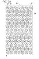
- FIG. 2A is a top view of the capacitive transducer of the present invention.
- Example 2 is approximately similar to Example 1 in the configuration of the capacitive transducer. Thus, the differences will be mainly described.
- the capacitive transducer in FIGS. 2A and 2B includes a second electrode 21, a first electrode 22, a gap 23, a sealing portion 26, a first membrane 27, a second membrane 28, a vibrating membrane 29, a substrate 30, a first insulating film 31, a cell 32, an element 34, and a second insulating film 35.
- the configuration is such that a dummy cell not electrically connected is arranged between active cells.
- the distances between neighboring cells are equal.
- the active cell is connected to a signal extraction electrode, the active cells are cells electrically connected in parallel, and the dummy cell is a cell that is not electrically connected with the active cell and does not perform transmission or reception of an ultrasound wave.
- the gaps between cells (in the broad sense), in the case where a cell is considered in the broad sense to include the active cell and the dummy cell are equal.
- the gap between cells (in the narrow sense) depends on the position of the element. For example, in FIG. 2A , the active cells are adjacent in a middle portion of the element such as in the sixth to eighth rows from the top, and the gap between the cells (in the narrow sense) is relatively narrow.
- the dummy cell is arranged in the second and ninth rows, and the gap between the neighboring cells (in the narrow sense) is large.
- the element of the capacitive transducer is formed of a plurality of cells, and the vibrating membrane vibrates in the case where each cell has transmitted or received an ultrasound wave. Due to a sound wave generated by the vibration of the vibrating membrane, acoustic crosstalk occurs between the respective cells.
- the acoustic crosstalk of the respective cells can be made the same.
- the transmission efficiency and the receiving sensitivity of all cells are approximately the same. Therefore, since a signal in an unnecessary frequency band is not transmitted or received, deterioration in the SN ratio can be prevented.
- the gap between cells in the end portion of the element is greater than the gap between cells in the middle portion of the element, as described above. Since the density of cells in the end portion of the element is lower than the density of cells in the middle portion of the element, the radiated sound pressure is smaller in the end portion of the element than in the middle portion of the element. Since the density of cells in the end portion of the element is lower than the density of cells in the middle portion of the element, the received sound pressure is smaller in the end portion of the element than in the middle portion of the element in a similar manner.
- a side lobe that occurs on the side of an ultrasound beam can be reduced. Interference by a side lobe can be reduced in a similar manner in the case of reception as well. Therefore, since an ultrasound signal not along the direction of an ultrasound beam and not from a target can be reduced and the SN ratio of a receive signal can be improved, a high-quality ultrasound image can be formed. Since the shape of all cells forming the element is the same, the transmission efficiency and the receiving sensitivity of all cells are the same. Therefore, since a signal in an unnecessary frequency band is not transmitted or received, deterioration in the SN ratio can be prevented.
- the capacitive transducer described above can be applied to a probe that receives or transmits an acoustic wave using the same.
- the probe 402 includes a plurality of elements 403.
- a transmission unit 405 performing control of a transmitted acoustic wave according to a command by an information processing unit 406, an acoustic wave is generated from each element.
- an electrical signal output from each element is subjected to processing (e.g., amplification or AD conversion) by a signal processing unit 404.
- FIG. 4 shows the probe described above being used as a component of an object information acquiring apparatus.
- a light absorber inside an object 401 absorbs light from a light source (not shown) to generate a photoacoustic wave
- the photoacoustic wave propagates inside the object and is received by the element.
- An electrical signal output from the element is input to the signal processing unit and subjected to signal processing.
- the information processing unit Based on a signal input from the signal processing unit, the information processing unit generates as characteristic information initial sound pressure distribution, absorption coefficient distribution, or the like of the inside of the object by known image reconstruction processing.
- Upon diagnosis, such information may be displayed in a display unit 407 as image data according to necessity.
- a configuration formed of the signal processing unit and the information processing unit may be referred to as processing unit.
- a case of acquiring echo information relating to the inside of an object With a control signal sent by the transmission unit at this time, an acoustic wave is transmitted from each element. The acoustic wave reflected at the acoustic impedance boundary inside the object is received again by the element. A receive signal output from the element is subjected to known signal processing, reconstruction processing, or image data generation, in a similar manner to the case of a photoacoustic wave. In the case of an apparatus using the reflected wave, a probe for transmission of an acoustic wave may be provided separately from a probe for reception.
- the capacitive transducer of the present invention can be applied to an apparatus having both functions as an apparatus using a photoacoustic wave and an apparatus using an echo wave.
- the probe may be for mechanical scanning or may be a probe (of a handheld type) that is grasped by a user such as a doctor or technician and moved with respect to an object. Particularly in the case of mechanically scanning an object that is a living body, stable measurement is made possible by holding the object with holding means. If the object is a breast, a plate-shaped or cup-shaped holding means is suitable.
- a side lobe in a capacitive transducer is reduced.
- a capacitive transducer including an element including a plurality of cells supported such that a vibrating membrane including one of a pair of electrodes formed with an gap inbetween is capable of vibration, wherein a distance between cells in an end portion of the element is greater than a distance between cells in a middle portion of the element.
Landscapes
- Physics & Mathematics (AREA)
- General Health & Medical Sciences (AREA)
- Immunology (AREA)
- Chemical & Material Sciences (AREA)
- Analytical Chemistry (AREA)
- Biochemistry (AREA)
- Health & Medical Sciences (AREA)
- General Physics & Mathematics (AREA)
- Life Sciences & Earth Sciences (AREA)
- Pathology (AREA)
- Engineering & Computer Science (AREA)
- Mechanical Engineering (AREA)
- Optics & Photonics (AREA)
- Transducers For Ultrasonic Waves (AREA)
- Ultra Sonic Daignosis Equipment (AREA)
Abstract
Description
- The present invention relates to a capacitive transducer and a method of manufacturing same.
- Conventionally, micromechanical components manufactured by micromachining technology have been processable in the order of micrometers. Through use thereof, various micro-functional elements have been realized. Capacitive transducers using such technology have been studied as a substitute for piezoelectric elements. With such a capacitive transducer, an ultrasound wave can be transmitted and received using vibration of a vibrating membrane, and excellent wideband characteristics particularly in liquid can be obtained easily.
- There is a capacitive transducer including an element in which cells are arranged in a square shape or rectangle shape and the gaps between adjacent cells are uniform (see Japanese Patent Application Laid-open No.
2008-98697 US Patent No. 8456958 ). - Patent Literature 1: Japanese Patent Application Laid-open No.
2008-98697 - Patent Literature 2:
US Patent No. 8456958 - In the case of transmitting an ultrasound wave with a capacitive transducer including an element in which cells are arranged in a square shape or rectangle shape and gaps between adjacent cells are uniform, the radiated sound pressure is uniform in an end portion and a middle portion of the element. Therefore, a side lobe of an ultrasound beam easily occurs. The quality of an ultrasound image using the ultrasound beam may deteriorate due to the side lobe. The image quality may deteriorate in a similar manner in the case of reception as well.
- In a capacitive transducer in which the transmission efficiency or receiving sensitivity of a cell in an end portion of an element is lower than in a middle portion, the structure is such that the shape of a cell in the end portion of the element and the shape of a cell in the middle portion of the element differ. With this configuration, apodization by which a side lobe is reduced is possible. Therefore, an ultrasound wave in an unnecessary frequency band may be transmitted or received at the time of transmitting or receiving an ultrasound wave to deteriorate the SN ratio.
- The present invention has been made based on recognition of such a task. The present invention is achieved to reduce a side lobe in a capacitive transducer.
- The present invention in its first aspect provides a capacitive transducer as specified in
claims 1 to 3, a probe as specified inclaim 4 or an object information acquiring apparatus as specified in claims 5 to 7. - The present invention in its second aspect provides a method of manufacturing a capacitive transducer as specified in
claim 8. - With the present invention, a side lobe in a capacitive transducer can be reduced.
- Further features of the present invention will become apparent from the following description of exemplary embodiments with reference to the attached drawings.
-
-
FIG. 1A is a top view of a capacitive transducer in Example 1; -
FIG. 1B is a sectional view along line A-B of the capacitive transducer in Example 1; -
FIG. 2A is a top view of a capacitive transducer in Example 2; -
FIG. 2B is a sectional view along line A-B of the capacitive transducer in Example 2; -
FIGS. 3A to 3E are sectional views along line A-B illustrating a method of preparing a capacitive transducer; and -
FIG. 4 is a block diagram illustrating the configuration of an object information acquiring apparatus. - A preferred embodiment of the present invention will be described below with reference to the drawings. Note that the dimension, material, and shape of components, the relative arrangement thereof, and the like described below should be changed appropriately depending on the configuration of an apparatus or various conditions to which the invention is applied and are not intended to limit the scope of the invention to the description below.
- The present invention has been made for a capacitive transducer for an ultrasound wave and can be applied to an apparatus and an method for transmitting or receiving an ultrasound wave using the transducer. Further, the subject matter of the present invention includes an apparatus utilizing an ultrasound echo technique in which an ultrasound wave is transmitted to an object such as a living body and an echo wave reflected and propagated inside the object is received. By data generation based on the echo wave, characteristic information reflecting the difference in acoustic impedance inside the object can be acquired.
- The capacitive transducer of the present invention can be utilized in receiving, besides an echo wave, a photoacoustic wave generated and propagated by a light absorber inside an object through a photoacoustic effect when the object is irradiated with light from a light source. By analyzing the photoacoustic wave, functional information or optical characteristic information relating to the inside of the object can be acquired. Such apparatuses obtain characteristic information by performing analysis with an information processing device after processing by a signal processing unit has been performed with respect to a received echo wave or photoacoustic wave, and therefore can be referred to as object information acquiring apparatus. By displaying the characteristic information as image data in a display unit, internal examination such as a diagnosis is possible.
- The present invention can also be understood as a method of controlling an object information acquiring apparatus, an object information acquiring method, or an acoustic wave measurement method. Further, the present invention can also be understood as a program that realizes such a method with an information processing unit such as a CPU or circuit. The present invention can also be understood as a method of manufacturing a capacitive transducer characteristic to the present invention or a method of manufacturing a probe using the same.
- In the case of using a capacitive transducer for acquiring characteristic information, use of a probe in which a single or a plurality of elements are arranged is preferable. By holding an object for scanning with the probe, measurement over a wide range is possible. If the object is a breast, it is preferable to use, for example, a plate-shaped member or cup-shaped member for holding.
- An ultrasound wave referred to in the present invention is given as a typical example of an acoustic wave also called a sound wave or elastic wave. The wavelength or the like is not limited.
- An embodiment of the present invention will be described below using
FIGS. 1A and1B .FIG. 1A is a top view of a capacitive transducer of the present invention, andFIG. 1B is a sectional view along line A-B inFIG. 1A . In anelement 14 of the capacitive transducer of the present invention, a plurality ofcells 12 are formed. The number of elements included in the capacitive transducer is one inFIG. 1A , but may any number. Herein, an element refers to each element of the capacitive transducer of which a signal extraction electrode is shared by all cells forming the element. That is, output of an electrical signal is performed in terms of the elements. The number of cells included in theelement 14 is sixty three inFIG. 1A , but may be any number. - In the cell, a vibrating
membrane 9 is supported to be capable of vibration. The vibratingmembrane 9 includes asecond electrode 1. Thesecond electrode 1 is provided such that afirst electrode 2 is across a gap 3 (i.e., cavity). InFIG. 1B , the vibrating membrane has a configuration in which thesecond electrode 1 is sandwiched between afirst membrane 7 and asecond membrane 8. However, a configuration with only the second electrode or only the first membrane and the second electrode is acceptable, as long as the vibrating membrane is capable of vibration and includes the second electrode. As will be described later,reference numeral 4 denotes an etching path,reference numeral 6 denotes a sealing portion,reference numeral 10 denotes a substrate, andreference numerals - The first electrode or the second electrode is used as an electrode for applying bias voltage or an electrode for adding an electrical signal or extracting an electrical signal. In this case, the first electrode is used as an electrode for applying bias voltage and the second electrode is used as a signal extraction electrode, but it may be the opposite. The electrode for applying bias voltage is also shared within an element. The configuration may be such that the bias voltage is shared between elements. However, the signal extraction electrode has to be electrically separated for each element.
- In the element of the capacitive transducer in
FIG. 1A , the gap between cells in an end portion of the element is greater than the gap between cells in a middle portion of the element. It is preferable that the gap between the cells become narrower from the end portion toward the middle portion of the element. It suffices that the gap between a pair of cells in the end portion of the element and the gap between a pair of cells in the middle portion of the element be designed depending on the shape of an intended ultrasound beam. For example, the design may be in accordance with the distribution of a Gaussian beam. Since the density of cells in the end portion of the element is lower than the density of cells in the middle portion of the element, the radiated sound pressure is smaller in the end portion of the element than in the middle portion of the element. Since the density of cells in the end portion of the element is lower than the density of cells in the middle portion of the element, the received sound pressure is smaller in the end portion of the element than in the middle portion of the element in a similar manner. - An ultrasound beam is radiated approximately perpendicularly from the element. This is generally called a main lobe. Further, a side lobe occurs as if to surround the main lobe. The side lobe is stronger when the wavelength of a transmitted or received ultrasound wave is shorter, the size of the element is greater, or the transmission efficiency or receiving sensitivity in the end portion of the element is higher.
- Thus, compared to a capacitive transducer having the same transmission efficiency or receiving sensitivity throughout an element from a middle portion to an end portion, a side lobe that occurs on the side of an ultrasound beam can be reduced. Interference by a side lobe can be reduced in a similar manner in the case of reception as well. Therefore, since an ultrasound signal not along the direction of an ultrasound beam and not from a target can be reduced and the SN ratio of a receive signal can be improved, a high-quality ultrasound image can be formed.
- Since the shape of all cells forming the element is the same, the transmission efficiency and the receiving sensitivity of all cells are the same. Therefore, since a signal in an unnecessary frequency band is not transmitted or received, deterioration in the SN ratio can be prevented. The shape of a cell is "the same," i.e., the shape may be exactly the same or may include an error, such as an error due to a manufacturing process, to a degree that the frequency characteristics of the conversion efficiency of a cell can be regarded the same.
- Since the shape of a vibrating membrane of all cells forming the element is the same, the radiation impedance of all cells is approximately the same. The radiation impedance refers to the ratio of force caused by the vibrating membrane pushing an acoustic medium such as liquid and the speed of the vibrating membrane, and shows the radiation capability. Since the radiation impedance of all cells is the same in this configuration, the transmission efficiency and the receiving sensitivity of all cells are approximately the same.
- Since the size of a vibrating membrane of all cells within the element can be made the same in this configuration, layout of a cell on a photomask is easy in the case of preparation with a semiconductor manufacturing process. In the case where a gap is 1 µm or less as in this configuration, the etching time for a sacrificial layer depends on the area of the sacrificial layer. Therefore, since the area of a sacrificial layer of all cells is the same in this configuration, the etching time for all cells can be made the same, and a capacitive transducer without a residue of a sacrificial layer and with a small variation in performance can be manufactured.
- Further, the configuration may be such that a dummy cell not electrically connected is arranged between active cells and the distances between neighboring cells (distances between overall positions including the active cell position and the dummy cell position) are equal. The active cell is connected to a signal extraction electrode, the active cells are cells electrically connected in parallel, and the dummy cell is a cell that is not electrically connected with the active cell and does not perform transmission or reception of an ultrasound wave. The distances between cells are "the same, "i.e., the distance between cells may be exactly the same or may include an error, such as an error due to a manufacturing process, to a degree that the acoustic crosstalk can be regarded the same.
- The element of the capacitive transducer is formed of a plurality of cells, and the vibrating membrane vibrates in the case where each cell has transmitted or received an ultrasound wave. Due to a sound wave generated by the vibration of the vibrating membrane, acoustic crosstalk occurs between the respective cells. By arranging the dummy cell between the active cells, the acoustic crosstalk of the respective cells can be made approximately the same. Thus, the transmission efficiency and the receiving sensitivity of all cells are approximately the same. Therefore, since a signal in an unnecessary frequency band is not transmitted or received, deterioration in the SN ratio can be prevented.
- Further, the configuration may be such that the gaps between all adjacent cells are the same. The transmission efficiency and the receiving sensitivity of all cells of the element of the capacitive transducer of this configuration are the same. Therefore, since a signal in an unnecessary frequency band is not transmitted or received, deterioration in the SN ratio can be prevented.
- The driving principle of the present invention will be described. By using a signal extraction wire, the capacitive transducer can extract an electrical signal from the second electrode. An electrical signal is extracted by an extraction wire in this embodiment, but a through wire or the like may be used. An electrical signal is extracted from the second electrode in this embodiment, but may be extracted from the first electrode.
- In the case of receiving an ultrasound wave with the capacitive transducer, a DC voltage is applied to the
first electrode 2 by voltage applying means (not shown) to generate a difference in potential between electrodes. In this case, it is recommended that thesecond electrode 1 be fixed at ground voltage. The ground voltage shows a reference potential in direct current of a current-voltage conversion circuit (receiving circuit) (not shown). When an ultrasound wave is incident, the vibratingmembrane 9 including thesecond electrode 1 is deformed. Therefore, the distance of thegap 3 between thesecond electrode 1 and thefirst electrode 2 changes, thereby changing the capacitance. Due to the change in capacitance, current is output from thesecond electrode 1, and current flows in an extraction wire. The current is converted into voltage by a current-voltage conversion circuit (not shown), and the ultrasound wave can be received. As described above, the configuration of an extraction wire may be changed such that a DC voltage is applied to the second electrode, and an electrical signal is extracted from the first electrode. The current-voltage conversion circuit is preferably provided within aprobe 402 inFIG. 4 . - In the case of transmitting an ultrasound wave, an AC voltage (including pulse voltage) is applied as a transmission signal to the
second electrode 1 in a state where a difference in potential is generated between thefirst electrode 2 and thesecond electrode 1, so that the vibratingmembrane 9 can be vibrated by the electrostatic force. Accordingly, an ultrasound wave can be transmitted. The configuration of an extraction wire may be changed in the case of transmission as well, such that an AC voltage is applied to the first electrode to vibrate a vibrating membrane. - Using
FIGS. 3A to 3E , one form of a preparation method of the this embodiment will be described.FIGS. 3A to 3E are sectional views of a capacitive transducer of the present invention of which the configuration is approximately similar toFIG. 1B .FIGS. 3A to 3E are sectional views along line A-B inFIG. 1A . - As shown in
FIG. 3A , a first insulatingfilm 61 is formed on asubstrate 60. Thesubstrate 60 is a silicon substrate, and the first insulatingfilm 61 is provided for insulation from a first electrode. In the case where thesubstrate 60 is an insulating substrate such as a glass substrate, the first insulatingfilm 61 may not be formed. Thesubstrate 60 is preferably a substrate with a small surface roughness. In the case where the surface roughness is large, the surface roughness is transferred in a membrane forming step that is a step after this step, causing variation among respective cells and respective elements in the distance between the first electrode and a second electrode due to the surface roughness. The variation results in variation in the sensitivity of transmission and reception. Therefore, thesubstrate 60 is preferably a substrate with a small surface roughness. - Next, a
first electrode 51 is formed. For thefirst electrode 51, a conductive material with a small surface roughness, e.g., titanium or aluminum, is preferable. In the case where the surface roughness of the first electrode is large, variation is caused among respective cells and respective elements in the distance between the first electrode and the second electrode due to the surface roughness in a similar manner to the substrate. Therefore, a conductive material with a small surface roughness is preferable. - Next, a second insulating
film 65 is formed. The second insulatingfilm 65 is formed preferably of an insulating material with a small surface roughness in order to prevent an electrical short circuit or dielectric breakdown between the first electrode and the second electrode in the case where voltage is applied between the first electrode and the second electrode. In the case of driving with low voltage, the second insulatingfilm 65 may not be formed, since a first membrane layer described later is an insulator. In the case where the surface roughness of the second insulating film is large, variation is caused among respective cells and respective elements in the distance between the first electrode and the second electrode due to the surface roughness in a similar manner to the substrate. Therefore, a second insulating film with a small surface roughness is preferable. Examples include a silicon nitride film and a silicon oxide film. - Next, as shown in
FIG. 3B , asacrificial layer 53 is formed. For thesacrificial layer 53, a material with a small surface roughness is preferable. In the case where the surface roughness of the sacrificial layer is large, variation is caused among respective cells and respective elements in the distance between the first electrode and the second electrode due to the surface roughness in a similar manner to the substrate. Therefore, a sacrificial layer with a small surface roughness is preferable. In order to shorten the time for etching in which the sacrificial layer is removed, a material with which the etching speed is fast is preferable. - The material of a sacrificial layer is desired to be such that the second insulating film, the first membrane layer, and the second electrode are almost not etched by etching liquid or etching gas for removing a sacrificial layer. In the case where the second insulating film, the first membrane layer, and the second electrode are nearly etched by etching liquid or etching gas for removing a sacrificial layer, variation in the thickness of a vibrating membrane and variation in the distance between the first electrode and the second electrode occur. The variation in thickness of the vibrating membrane and the variation in the distance between the first electrode and the second electrode become variation in sensitivity among respective cells and among respective elements. In the case where the second insulating film and the first membrane layer are a silicon nitride film or silicon oxide film, chromium with a small surface roughness and for which an etching liquid does not cause etching of the second insulating film, the first membrane layer, and the second electrode is preferable.
- With
FIGS. 3C to 3E , steps of forming the vibrating membrane including the second electrode and forming a gap through removal of a sacrificial layer will be described. The vibrating membrane is formed of a first membrane, the second electrode, and a second membrane inFIGS. 3A to 3E , but may be formed with any number of layers as long as the second electrode is included. - As shown in
FIG. 3C , afirst membrane layer 57 including the first membrane is formed. For thefirst membrane layer 57, low tensile stress is preferable. For example, tensile stress of 300 MPa or less is preferable. With a silicon nitride film, control of stress is possible, and the tensile stress can be made 300 MPa or less. In the case where the first membrane has compressive stress, the first membrane becomes highly deformed due to sticking or buckling. In the case of large tensile stress, the first membrane may be broken. Therefore, for thefirst membrane layer 57, low tensile stress is preferable. - Next, as shown in
FIG. 3D , asecond electrode 52 is formed, and an etching hole (not shown) is further formed. Then, thesacrificial layer 53 is removed through the etching hole via an etching path (not shown). For thesecond electrode 52, a material with small residual stress and having heat resistance is preferable. In the case where residual stress of the second electrode is large, the vibrating membrane becomes highly deformed. Therefore, a second electrode with small residual stress is preferable. It is preferable that a material not cause transformation or an increase in stress depending on the temperature or the like upon forming a second membrane layer or a sealing layer for forming a sealing portion. - In the case of performing removal of the sacrificial layer in a state where the second electrode is exposed, etching of the sacrificial layer needs to be performed while a photoresist or the like for protection of the second electrode is applied. Since stress due to the photoresist or the like facilitates sticking of the first membrane, it is preferable that the second electrode have etching resistance such that etching of the sacrificial layer is feasible in a state where the second electrode is exposed without a photoresist. Sticking refers to the adhesion of the vibrating membrane as a structure after removal of the sacrificial layer. For example, titanium, aluminum-silicon alloy or the like is preferable.
- Next, as shown in
FIG. 3E , asecond membrane layer 58 including the second membrane is formed. In this step, the second membrane is formed, and the sealing portion for sealing the etching hole (not shown) is formed. By forming thesecond membrane layer 58, the second membrane is formed to form the vibrating membrane having a desired spring constant and enable sealing of the etching hole. - In the case where a step of sealing the etching hole and a step of forming the second membrane are the same as in this step, the vibrating membrane can be formed with only the membrane forming step. Therefore, since it is easy to control the thickness of the vibrating membrane and variation in the spring constant or variation in the deflection of the vibrating membrane due to variation in the thickness can be reduced, variation in the receiving or transmitting sensitivity among cells or elements can be reduced.
- The step of sealing the etching hole and the step of forming the second membrane may be separate steps. It may be such that the sealing portion is formed after the second membrane is formed, or the second membrane is formed after the sealing portion is formed.
- For the second membrane layer, a material having low tensile stress is preferable. In the case where the second membrane has compressive stress in a similar manner to the first membrane, the first membrane becomes highly deformed due to sticking or buckling. In the case of large tensile stress, the second membrane may be broken. Therefore, for the second membrane layer, low tensile stress is preferable. With a silicon nitride film, control of stress is possible, and the tensile stress can be made 300 MPa or less.
- For the sealing portion, it suffices that liquid or external air be prevented from entering into the gap. Particularly, in the case of sealing under reduced pressure, the vibrating membrane is deformed by atmospheric pressure, and the distance between the first electrode and the second electrode decreases. Since the transmitting or receiving sensitivity is proportional to the effective distance between the first electrode and the second electrode raised to the power of 1.5, the transmitting or receiving sensitivity can be improved through sealing under reduced pressure such that the pressure in the gap is lower than the atmospheric pressure. The effective distance takes into consideration the gap and a value for the insulating film for the first electrode and the second electrode obtained through division by the dielectric constant.
- After this step, a wire connecting the first electrode and the second electrode is formed by a step that is not shown. The material for the wire may be aluminum or the like.
- With such a manufacturing method, a capacitive transducer having a configuration necessary for achieving the object of the present invention can be manufactured.
- A more specific example will be given below for a detailed description of the present invention.
- An embodiment of the present invention will be described below using
FIGS. 1A and1B .FIG. 1A is a top view of the capacitive transducer of the present invention, andFIG. 1B is a sectional view along line A-B inFIG. 1A . Theelement 14 of the capacitive transducer of the present invention is formed of sixty-threecells 12. The number of elements included in the capacitive transducer is one inFIG. 1A , but may any number. - The
cell 12 is supported such that the vibratingmembrane 9 including thesecond electrode 1 provided across thegap 3 from thefirst electrode 2 is capable of vibration. The vibratingmembrane 9 has a configuration in which thesecond electrode 1 is sandwiched between thefirst membrane 7 and thesecond membrane 8. Thefirst electrode 2 is an electrode for applying bias voltage, and thesecond electrode 1 is a signal extraction electrode. The shape of the vibrating membrane in this example is a circle. However, the shape may be a quadrangle, hexagon, or the like. In the case of a circle, the vibrational mode is axisymmetric. Therefore, vibration of the vibrating membrane due to an unnecessary vibrational mode can be reduced. - The first insulating
film 11 on thesilicon substrate 10 is a silicon oxide film formed by thermal oxidation and with a thickness of 1 µm. The second insulatingfilm 15 is a silicon oxide film formed by plasma-enhanced chemical vapor deposition (PE-CVD) and with a thickness of 0.1 µm. The first electrode is aluminum with a thickness of 50 nm, and thesecond electrode 1 is aluminum with a thickness of 100 nm. Thefirst membrane 7 and thesecond membrane 8 are silicon nitride films prepared by PE-CVD and are formed with tensile stress of 200 MPa or less. The diameter of thefirst membrane 7 and thesecond membrane 8 is 25 µm. The respective thicknesses are 0.4 µm and 0.7 µm. - In the element of the capacitive transducer in
FIG. 1A , the gap between cells in the end portion of the element is greater than the gap between cells in the middle portion of the element. Since the density of cells in the end portion of the element is lower than the density of cells in the middle portion of the element, the radiated sound pressure is smaller in the end portion of the element than in the middle portion of the element. Since the density of cells in the end portion of the element is lower than the density of cells in the middle portion of the element, the received sound pressure is smaller in the end portion of the element than in the middle portion of the element in a similar manner. Thus, compared to a capacitive transducer having the same transmission efficiency or receiving sensitivity throughout an element from a middle portion to an end portion, a side lobe that occurs on the side of an ultrasound beam can be reduced. Therefore, an ultrasound signal not along the direction of an ultrasound beam and not from a target can be reduced, and a high-quality ultrasound image can be formed. Since the shape of all cells forming the element is the same, the transmission efficiency and the receiving sensitivity of all cells are the same. Therefore, since a signal in an unnecessary frequency band is not transmitted or received, deterioration in the SN ratio can be prevented. - Since the shape of a vibrating membrane of all cells forming the element is the same, the radiation impedance of all cells is approximately the same. Since the radiation impedance of all cells is the same in this configuration, the transmission efficiency and the receiving sensitivity of all cells are approximately the same.
- Since the size of a vibrating membrane of all cells within the element can be made the same in this configuration, layout of a cell on a photomask is easy in the case of preparation with a semiconductor manufacturing process. In the case where the gap is 1 µm or less as in this configuration, the etching time for a sacrificial layer depends on the area of the sacrificial layer. Therefore, since the area of a sacrificial layer of all cells is the same in this configuration, the etching time for all cells can be made the same, and a capacitive transducer without a residue of a sacrificial layer and with a small variation in performance can be manufactured.
- The shape of a vibrating membrane of a cell is the same within the element, and only the arrangement of a cell when seen from above is not uniform. Thus, in the case of preparing the capacitive transducer of the present invention using a semiconductor manufacturing process, preparation is feasible with the same manufacturing method as for a capacitive transducer in which the cell arrangement is uniform.
- The configuration of a capacitive transducer of Example 2 will be described using
FIGS. 2A and2B .FIG. 2A is a top view of the capacitive transducer of the present invention. Example 2 is approximately similar to Example 1 in the configuration of the capacitive transducer. Thus, the differences will be mainly described. - The capacitive transducer in
FIGS. 2A and2B includes asecond electrode 21, afirst electrode 22, agap 23, a sealingportion 26, afirst membrane 27, asecond membrane 28, a vibratingmembrane 29, asubstrate 30, a first insulatingfilm 31, acell 32, anelement 34, and a second insulatingfilm 35. - In the element of the capacitive transducer in
FIG. 2A , the configuration is such that a dummy cell not electrically connected is arranged between active cells. The distances between neighboring cells (distances between cell positions, in the case where a cell position is taken in the broad sense to include the active cell position and the dummy cell position) are equal. The active cell is connected to a signal extraction electrode, the active cells are cells electrically connected in parallel, and the dummy cell is a cell that is not electrically connected with the active cell and does not perform transmission or reception of an ultrasound wave. - In the case of this example, the gaps between cells (in the broad sense), in the case where a cell is considered in the broad sense to include the active cell and the dummy cell, are equal. In the case where a cell is considered in the narrow sense as only the active cell (relating to ultrasound wave transmission or reception), the gap between cells (in the narrow sense) depends on the position of the element. For example, in
FIG. 2A , the active cells are adjacent in a middle portion of the element such as in the sixth to eighth rows from the top, and the gap between the cells (in the narrow sense) is relatively narrow. Toward the end portion of the element, the dummy cell is arranged in the second and ninth rows, and the gap between the neighboring cells (in the narrow sense) is large. - The element of the capacitive transducer is formed of a plurality of cells, and the vibrating membrane vibrates in the case where each cell has transmitted or received an ultrasound wave. Due to a sound wave generated by the vibration of the vibrating membrane, acoustic crosstalk occurs between the respective cells. With a configuration in which the dummy cell is arranged between the active cells and all distances between the cells (in the broad sense) are equal, the acoustic crosstalk of the respective cells can be made the same. Thus, the transmission efficiency and the receiving sensitivity of all cells are approximately the same. Therefore, since a signal in an unnecessary frequency band is not transmitted or received, deterioration in the SN ratio can be prevented.
- In the capacitive transducer according to the present invention, the gap between cells in the end portion of the element is greater than the gap between cells in the middle portion of the element, as described above. Since the density of cells in the end portion of the element is lower than the density of cells in the middle portion of the element, the radiated sound pressure is smaller in the end portion of the element than in the middle portion of the element. Since the density of cells in the end portion of the element is lower than the density of cells in the middle portion of the element, the received sound pressure is smaller in the end portion of the element than in the middle portion of the element in a similar manner.
- Thus, compared to a capacitive transducer having the same transmission efficiency or receiving sensitivity throughout an element from a middle portion to an end portion, a side lobe that occurs on the side of an ultrasound beam can be reduced. Interference by a side lobe can be reduced in a similar manner in the case of reception as well. Therefore, since an ultrasound signal not along the direction of an ultrasound beam and not from a target can be reduced and the SN ratio of a receive signal can be improved, a high-quality ultrasound image can be formed. Since the shape of all cells forming the element is the same, the transmission efficiency and the receiving sensitivity of all cells are the same. Therefore, since a signal in an unnecessary frequency band is not transmitted or received, deterioration in the SN ratio can be prevented.
- The capacitive transducer described above can be applied to a probe that receives or transmits an acoustic wave using the same. For example, in
FIG. 4 , theprobe 402 includes a plurality ofelements 403. By atransmission unit 405 performing control of a transmitted acoustic wave according to a command by aninformation processing unit 406, an acoustic wave is generated from each element. At the time of reception, an electrical signal output from each element is subjected to processing (e.g., amplification or AD conversion) by asignal processing unit 404. -
FIG. 4 shows the probe described above being used as a component of an object information acquiring apparatus. - First, a case where a light absorber inside an
object 401 absorbs light from a light source (not shown) to generate a photoacoustic wave will be described. At this time, the photoacoustic wave propagates inside the object and is received by the element. An electrical signal output from the element is input to the signal processing unit and subjected to signal processing. Based on a signal input from the signal processing unit, the information processing unit generates as characteristic information initial sound pressure distribution, absorption coefficient distribution, or the like of the inside of the object by known image reconstruction processing. Upon diagnosis, such information may be displayed in adisplay unit 407 as image data according to necessity. In this specification, a configuration formed of the signal processing unit and the information processing unit may be referred to as processing unit. - Next, a case of acquiring echo information relating to the inside of an object will be described. With a control signal sent by the transmission unit at this time, an acoustic wave is transmitted from each element. The acoustic wave reflected at the acoustic impedance boundary inside the object is received again by the element. A receive signal output from the element is subjected to known signal processing, reconstruction processing, or image data generation, in a similar manner to the case of a photoacoustic wave. In the case of an apparatus using the reflected wave, a probe for transmission of an acoustic wave may be provided separately from a probe for reception.
- Further, the capacitive transducer of the present invention can be applied to an apparatus having both functions as an apparatus using a photoacoustic wave and an apparatus using an echo wave.
- The probe may be for mechanical scanning or may be a probe (of a handheld type) that is grasped by a user such as a doctor or technician and moved with respect to an object. Particularly in the case of mechanically scanning an object that is a living body, stable measurement is made possible by holding the object with holding means. If the object is a breast, a plate-shaped or cup-shaped holding means is suitable.
- While the present invention has been described with reference to exemplary embodiments, it is to be understood that the invention is not limited to the disclosed exemplary embodiments. The scope of the following claims is to be accorded the broadest interpretation so as to encompass all such modifications and equivalent structures and functions.
- A side lobe in a capacitive transducer is reduced. Provided is a capacitive transducer including an element including a plurality of cells supported such that a vibrating membrane including one of a pair of electrodes formed with an gap inbetween is capable of vibration, wherein a distance between cells in an end portion of the element is greater than a distance between cells in a middle portion of the element.
Claims (8)
- A capacitive transducer comprising:an element including a plurality of cells supported such that a vibrating membrane including one of a pair of electrodes formed with an gap inbetween is capable of vibration, whereina distance between cells in an end portion of the element is greater than a distance between cells in a middle portion of the element.
- The capacitive transducer according to claim 1, wherein the plurality of cells are active cells electrically connected in parallel, and the element is arranged with the active cells and dummy cells not electrically connected.
- The capacitive transducer according to claim 2, wherein distances for the adjacent active cells or dummy cells are equal.
- A probe comprising a capacitive transducer according to any one of claims 1 to 3.
- An object information acquiring apparatus comprising:a capacitive transducer according to any one of claims 1 to 3; anda processing unit in which an electrical signal, output from the capacitive transducer due to an acoustic wave propagated from an object being incident upon the vibrating membrane, is used to acquire characteristic information relating to an inside of the object.
- The object information acquiring apparatus according to claim 5, further comprising a transmission unit with which the vibrating membrane is vibrated by applying voltage to the pair of electrodes to cause transmission of an acoustic wave, wherein
the acoustic wave is a reflection of the transmitted acoustic wave from an inside of the object. - The object information acquiring apparatus according to claim 5, further comprising a light source, wherein
the acoustic wave is a photoacoustic wave generated from the object irradiated with light from the light source. - A method of manufacturing a capacitive transducer including an element including a plurality of cells,
the method comprising the steps of:forming a plurality of first electrodes; andforming a vibrating membrane capable of vibration and including a plurality of second electrodes paired with the plurality of first electrodes respectively to thereby form a plurality of the cells including a pair of the first electrode and the second electrode, whereina distance between cells in an end portion of the element is made greater than a distance between cells in a middle portion of the element in the step of formation.
Applications Claiming Priority (2)
| Application Number | Priority Date | Filing Date | Title |
|---|---|---|---|
| JP2013092668A JP6238556B2 (en) | 2013-04-25 | 2013-04-25 | Subject information acquisition apparatus, control method therefor, and probe |
| JP2014022480A JP6395391B2 (en) | 2014-02-07 | 2014-02-07 | Capacitive transducer and manufacturing method thereof |
Publications (3)
| Publication Number | Publication Date |
|---|---|
| EP2796209A2 true EP2796209A2 (en) | 2014-10-29 |
| EP2796209A3 EP2796209A3 (en) | 2015-06-10 |
| EP2796209B1 EP2796209B1 (en) | 2020-06-17 |
Family
ID=50439246
Family Applications (1)
| Application Number | Title | Priority Date | Filing Date |
|---|---|---|---|
| EP14163663.9A Active EP2796209B1 (en) | 2013-04-25 | 2014-04-07 | Capacitive transducer and method of manufacturing the same |
Country Status (3)
| Country | Link |
|---|---|
| US (1) | US10189049B2 (en) |
| EP (1) | EP2796209B1 (en) |
| CN (1) | CN104117476B (en) |
Families Citing this family (6)
| Publication number | Priority date | Publication date | Assignee | Title |
|---|---|---|---|---|
| JP6429711B2 (en) | 2015-03-31 | 2018-11-28 | キヤノン株式会社 | Probe and subject information acquisition apparatus using the probe |
| JP6606034B2 (en) * | 2016-08-24 | 2019-11-13 | 株式会社日立製作所 | Capacitive detection type ultrasonic transducer and ultrasonic imaging apparatus including the same |
| CN108296155B (en) * | 2018-02-12 | 2022-12-16 | 浙江大学 | Micro-electromechanical piezoelectric ultrasonic transducer with V-shaped spring |
| JP7195759B2 (en) | 2018-04-20 | 2022-12-26 | キヤノン株式会社 | Photoacoustic device and object information acquisition method |
| WO2019213388A1 (en) * | 2018-05-03 | 2019-11-07 | Butterfly Network, Inc. | Pressure port for ultrasonic transducer on cmos sensor |
| CN114367431B (en) * | 2022-01-10 | 2023-05-23 | 京东方科技集团股份有限公司 | Transducer and preparation method thereof |
Citations (2)
| Publication number | Priority date | Publication date | Assignee | Title |
|---|---|---|---|---|
| JP2008098697A (en) | 2006-10-05 | 2008-04-24 | Hitachi Ltd | Ultrasonic transducer and manufacturing method thereof |
| US8456958B2 (en) | 2006-02-21 | 2013-06-04 | Vermon S.A. | Capacitive micro-machined ultrasonic transducer for element transducer apertures |
Family Cites Families (35)
| Publication number | Priority date | Publication date | Assignee | Title |
|---|---|---|---|---|
| US2837728A (en) * | 1945-12-14 | 1958-06-03 | Schuck Oscar Hugo | Means to alter the directivity pattern of energy translating devices |
| JPH0124479Y2 (en) | 1980-01-18 | 1989-07-25 | ||
| JPS5896200U (en) | 1981-12-22 | 1983-06-30 | タイガー魔法瓶株式会社 | Gas cylinder connection device for simple gas stove |
| US4425525A (en) | 1982-02-16 | 1984-01-10 | General Electric Company | Ultrasonic transducer array shading |
| US4460841A (en) | 1982-02-16 | 1984-07-17 | General Electric Company | Ultrasonic transducer shading |
| GB8912782D0 (en) * | 1989-06-02 | 1989-07-19 | Udi Group Ltd | An acoustic transducer |
| JPH06125894A (en) | 1992-10-14 | 1994-05-10 | Fujitsu Ltd | Ultrasonic probe |
| DE4428500C2 (en) | 1993-09-23 | 2003-04-24 | Siemens Ag | Ultrasonic transducer array with a reduced number of transducer elements |
| US5488956A (en) * | 1994-08-11 | 1996-02-06 | Siemens Aktiengesellschaft | Ultrasonic transducer array with a reduced number of transducer elements |
| US5619476A (en) * | 1994-10-21 | 1997-04-08 | The Board Of Trustees Of The Leland Stanford Jr. Univ. | Electrostatic ultrasonic transducer |
| JP3210252B2 (en) | 1996-07-10 | 2001-09-17 | 東海興業株式会社 | Extrusion molding equipment for vehicle molding |
| JP3254382B2 (en) | 1996-07-12 | 2002-02-04 | 株式会社イノアックコーポレーション | Extrusion mold structure |
| US6381197B1 (en) * | 1999-05-11 | 2002-04-30 | Bernard J Savord | Aperture control and apodization in a micro-machined ultrasonic transducer |
| US6359367B1 (en) * | 1999-12-06 | 2002-03-19 | Acuson Corporation | Micromachined ultrasonic spiral arrays for medical diagnostic imaging |
| JP4370120B2 (en) | 2003-05-26 | 2009-11-25 | オリンパス株式会社 | Ultrasound endoscope and ultrasound endoscope apparatus |
| JP2004350703A (en) | 2003-05-26 | 2004-12-16 | Olympus Corp | Ultrasonic diagnosis probe apparatus |
| JP4294376B2 (en) | 2003-05-26 | 2009-07-08 | オリンパス株式会社 | Ultrasonic diagnostic probe device |
| US20050075572A1 (en) | 2003-10-01 | 2005-04-07 | Mills David M. | Focusing micromachined ultrasonic transducer arrays and related methods of manufacture |
| JP2005117159A (en) | 2003-10-03 | 2005-04-28 | Fuji Photo Film Co Ltd | Ultrasonic transducer array and manufacturing method therefor |
| DE602005006419T2 (en) | 2005-09-14 | 2008-09-25 | Esaote S.P.A. | Electroacoustic transducer for high frequency applications |
| US7745973B2 (en) * | 2006-05-03 | 2010-06-29 | The Board Of Trustees Of The Leland Stanford Junior University | Acoustic crosstalk reduction for capacitive micromachined ultrasonic transducers in immersion |
| US7892176B2 (en) * | 2007-05-02 | 2011-02-22 | General Electric Company | Monitoring or imaging system with interconnect structure for large area sensor array |
| JP5305993B2 (en) | 2008-05-02 | 2013-10-02 | キヤノン株式会社 | Capacitive electromechanical transducer manufacturing method and capacitive electromechanical transducer |
| JP5578836B2 (en) | 2008-12-25 | 2014-08-27 | キヤノン株式会社 | Electromechanical transducer and method for manufacturing the same |
| JP5312081B2 (en) | 2009-02-10 | 2013-10-09 | キヤノン株式会社 | Biological information processing apparatus and biological information processing method |
| JP5377066B2 (en) | 2009-05-08 | 2013-12-25 | キヤノン株式会社 | Capacitive electromechanical transducer and method for producing the same |
| JP5578810B2 (en) | 2009-06-19 | 2014-08-27 | キヤノン株式会社 | Capacitance type electromechanical transducer |
| JP5574674B2 (en) | 2009-11-12 | 2014-08-20 | キヤノン株式会社 | Acoustic wave measuring device |
| IT1398262B1 (en) * | 2010-02-23 | 2013-02-22 | Esaote Spa | ULTRASOUND PROBE. |
| JP2012217624A (en) | 2011-04-08 | 2012-11-12 | Canon Inc | Subject information obtaining apparatus, subject information obtaining method, and program |
| JP5950517B2 (en) | 2011-09-02 | 2016-07-13 | キヤノン株式会社 | Subject information acquisition apparatus, subject information acquisition method, and program |
| JP5943677B2 (en) | 2012-03-31 | 2016-07-05 | キヤノン株式会社 | Probe and subject information acquisition apparatus using the probe |
| JP6071285B2 (en) | 2012-07-06 | 2017-02-01 | キヤノン株式会社 | Capacitive transducer |
| JP2012234208A (en) | 2012-08-23 | 2012-11-29 | Seiko Epson Corp | Wavelength variable filter |
| JP6315893B2 (en) | 2013-04-18 | 2018-04-25 | キヤノン株式会社 | Subject information acquisition apparatus, subject information acquisition method, and program |
-
2014
- 2014-04-07 EP EP14163663.9A patent/EP2796209B1/en active Active
- 2014-04-14 US US14/251,735 patent/US10189049B2/en active Active
- 2014-04-25 CN CN201410171904.0A patent/CN104117476B/en active Active
Patent Citations (2)
| Publication number | Priority date | Publication date | Assignee | Title |
|---|---|---|---|---|
| US8456958B2 (en) | 2006-02-21 | 2013-06-04 | Vermon S.A. | Capacitive micro-machined ultrasonic transducer for element transducer apertures |
| JP2008098697A (en) | 2006-10-05 | 2008-04-24 | Hitachi Ltd | Ultrasonic transducer and manufacturing method thereof |
Also Published As
| Publication number | Publication date |
|---|---|
| US10189049B2 (en) | 2019-01-29 |
| CN104117476A (en) | 2014-10-29 |
| US20140318254A1 (en) | 2014-10-30 |
| EP2796209A3 (en) | 2015-06-10 |
| CN104117476B (en) | 2019-11-15 |
| EP2796209B1 (en) | 2020-06-17 |
Similar Documents
| Publication | Publication Date | Title |
|---|---|---|
| US10293374B2 (en) | Capacitive transducer and method of manufacturing same | |
| KR101954102B1 (en) | Capacitive transducer, capacitive transducer manufacturing method, and object information acquisition apparatus | |
| EP2796209B1 (en) | Capacitive transducer and method of manufacturing the same | |
| EP2840060B1 (en) | Method for manufacturing a capacitive transducer | |
| JP2020057860A (en) | Capacitive transducer and method of manufacturing the same | |
| EP2792423A2 (en) | Transducer, method for manufacturing transducer, and object information acquiring apparatus | |
| Lu | Piezoelectric micromachined ultrasonic transducers for fingerprint sensing | |
| JP6395391B2 (en) | Capacitive transducer and manufacturing method thereof | |
| JP6395390B2 (en) | Capacitive transducer and manufacturing method thereof | |
| US10119855B2 (en) | Capacitance type transducer | |
| US10139338B2 (en) | Electromechanical transducer | |
| US10371569B2 (en) | Electrostatic capacitance type transducer | |
| JP6147138B2 (en) | Capacitive transducer and manufacturing method thereof | |
| JP2020018469A (en) | Electrostatic capacity type transducer and ultrasonic probe using the same | |
| Sadeghpour et al. | Klik hier als u tekst wilt invoeren. Bendable Piezoele | |
| JP2015186157A (en) | Electrostatic capacity type transducer | |
| JP2015115631A (en) | Electrostatic capacity type transducer, and method for manufacturing the same | |
| JP2015213224A (en) | Manufacturing method of capacitive transducer, and capacitive transducer |
Legal Events
| Date | Code | Title | Description |
|---|---|---|---|
| PUAI | Public reference made under article 153(3) epc to a published international application that has entered the european phase |
Free format text: ORIGINAL CODE: 0009012 |
|
| 17P | Request for examination filed |
Effective date: 20140407 |
|
| AK | Designated contracting states |
Kind code of ref document: A2 Designated state(s): AL AT BE BG CH CY CZ DE DK EE ES FI FR GB GR HR HU IE IS IT LI LT LU LV MC MK MT NL NO PL PT RO RS SE SI SK SM TR |
|
| AX | Request for extension of the european patent |
Extension state: BA ME |
|
| PUAL | Search report despatched |
Free format text: ORIGINAL CODE: 0009013 |
|
| AK | Designated contracting states |
Kind code of ref document: A3 Designated state(s): AL AT BE BG CH CY CZ DE DK EE ES FI FR GB GR HR HU IE IS IT LI LT LU LV MC MK MT NL NO PL PT RO RS SE SI SK SM TR |
|
| AX | Request for extension of the european patent |
Extension state: BA ME |
|
| RIC1 | Information provided on ipc code assigned before grant |
Ipc: B06B 1/06 20060101AFI20150506BHEP |
|
| R17P | Request for examination filed (corrected) |
Effective date: 20151210 |
|
| RBV | Designated contracting states (corrected) |
Designated state(s): AL AT BE BG CH CY CZ DE DK EE ES FI FR GB GR HR HU IE IS IT LI LT LU LV MC MK MT NL NO PL PT RO RS SE SI SK SM TR |
|
| STAA | Information on the status of an ep patent application or granted ep patent |
Free format text: STATUS: EXAMINATION IS IN PROGRESS |
|
| 17Q | First examination report despatched |
Effective date: 20180906 |
|
| REG | Reference to a national code |
Ref country code: DE Ref legal event code: R079 Ref document number: 602014066615 Country of ref document: DE Free format text: PREVIOUS MAIN CLASS: B06B0001060000 Ipc: B06B0001020000 |
|
| GRAP | Despatch of communication of intention to grant a patent |
Free format text: ORIGINAL CODE: EPIDOSNIGR1 |
|
| STAA | Information on the status of an ep patent application or granted ep patent |
Free format text: STATUS: GRANT OF PATENT IS INTENDED |
|
| RIC1 | Information provided on ipc code assigned before grant |
Ipc: B06B 1/02 20060101AFI20190716BHEP |
|
| INTG | Intention to grant announced |
Effective date: 20190731 |
|
| RIN1 | Information on inventor provided before grant (corrected) |
Inventor name: NAGAE, KENICHI Inventor name: TORASHIMA, KAZUTOSHI |
|
| GRAJ | Information related to disapproval of communication of intention to grant by the applicant or resumption of examination proceedings by the epo deleted |
Free format text: ORIGINAL CODE: EPIDOSDIGR1 |
|
| STAA | Information on the status of an ep patent application or granted ep patent |
Free format text: STATUS: EXAMINATION IS IN PROGRESS |
|
| GRAP | Despatch of communication of intention to grant a patent |
Free format text: ORIGINAL CODE: EPIDOSNIGR1 |
|
| STAA | Information on the status of an ep patent application or granted ep patent |
Free format text: STATUS: GRANT OF PATENT IS INTENDED |
|
| INTC | Intention to grant announced (deleted) | ||
| INTG | Intention to grant announced |
Effective date: 20200107 |
|
| GRAS | Grant fee paid |
Free format text: ORIGINAL CODE: EPIDOSNIGR3 |
|
| GRAA | (expected) grant |
Free format text: ORIGINAL CODE: 0009210 |
|
| STAA | Information on the status of an ep patent application or granted ep patent |
Free format text: STATUS: THE PATENT HAS BEEN GRANTED |
|
| AK | Designated contracting states |
Kind code of ref document: B1 Designated state(s): AL AT BE BG CH CY CZ DE DK EE ES FI FR GB GR HR HU IE IS IT LI LT LU LV MC MK MT NL NO PL PT RO RS SE SI SK SM TR |
|
| REG | Reference to a national code |
Ref country code: GB Ref legal event code: FG4D |
|
| REG | Reference to a national code |
Ref country code: CH Ref legal event code: EP |
|
| REG | Reference to a national code |
Ref country code: IE Ref legal event code: FG4D |
|
| REG | Reference to a national code |
Ref country code: DE Ref legal event code: R096 Ref document number: 602014066615 Country of ref document: DE |
|
| REG | Reference to a national code |
Ref country code: AT Ref legal event code: REF Ref document number: 1280686 Country of ref document: AT Kind code of ref document: T Effective date: 20200715 |
|
| PG25 | Lapsed in a contracting state [announced via postgrant information from national office to epo] |
Ref country code: NO Free format text: LAPSE BECAUSE OF FAILURE TO SUBMIT A TRANSLATION OF THE DESCRIPTION OR TO PAY THE FEE WITHIN THE PRESCRIBED TIME-LIMIT Effective date: 20200917 Ref country code: FI Free format text: LAPSE BECAUSE OF FAILURE TO SUBMIT A TRANSLATION OF THE DESCRIPTION OR TO PAY THE FEE WITHIN THE PRESCRIBED TIME-LIMIT Effective date: 20200617 Ref country code: GR Free format text: LAPSE BECAUSE OF FAILURE TO SUBMIT A TRANSLATION OF THE DESCRIPTION OR TO PAY THE FEE WITHIN THE PRESCRIBED TIME-LIMIT Effective date: 20200918 Ref country code: SE Free format text: LAPSE BECAUSE OF FAILURE TO SUBMIT A TRANSLATION OF THE DESCRIPTION OR TO PAY THE FEE WITHIN THE PRESCRIBED TIME-LIMIT Effective date: 20200617 Ref country code: LT Free format text: LAPSE BECAUSE OF FAILURE TO SUBMIT A TRANSLATION OF THE DESCRIPTION OR TO PAY THE FEE WITHIN THE PRESCRIBED TIME-LIMIT Effective date: 20200617 |
|
| REG | Reference to a national code |
Ref country code: LT Ref legal event code: MG4D |
|
| REG | Reference to a national code |
Ref country code: NL Ref legal event code: MP Effective date: 20200617 |
|
| PG25 | Lapsed in a contracting state [announced via postgrant information from national office to epo] |
Ref country code: HR Free format text: LAPSE BECAUSE OF FAILURE TO SUBMIT A TRANSLATION OF THE DESCRIPTION OR TO PAY THE FEE WITHIN THE PRESCRIBED TIME-LIMIT Effective date: 20200617 Ref country code: RS Free format text: LAPSE BECAUSE OF FAILURE TO SUBMIT A TRANSLATION OF THE DESCRIPTION OR TO PAY THE FEE WITHIN THE PRESCRIBED TIME-LIMIT Effective date: 20200617 Ref country code: BG Free format text: LAPSE BECAUSE OF FAILURE TO SUBMIT A TRANSLATION OF THE DESCRIPTION OR TO PAY THE FEE WITHIN THE PRESCRIBED TIME-LIMIT Effective date: 20200917 Ref country code: LV Free format text: LAPSE BECAUSE OF FAILURE TO SUBMIT A TRANSLATION OF THE DESCRIPTION OR TO PAY THE FEE WITHIN THE PRESCRIBED TIME-LIMIT Effective date: 20200617 |
|
| REG | Reference to a national code |
Ref country code: AT Ref legal event code: MK05 Ref document number: 1280686 Country of ref document: AT Kind code of ref document: T Effective date: 20200617 |
|
| PG25 | Lapsed in a contracting state [announced via postgrant information from national office to epo] |
Ref country code: NL Free format text: LAPSE BECAUSE OF FAILURE TO SUBMIT A TRANSLATION OF THE DESCRIPTION OR TO PAY THE FEE WITHIN THE PRESCRIBED TIME-LIMIT Effective date: 20200617 Ref country code: AL Free format text: LAPSE BECAUSE OF FAILURE TO SUBMIT A TRANSLATION OF THE DESCRIPTION OR TO PAY THE FEE WITHIN THE PRESCRIBED TIME-LIMIT Effective date: 20200617 |
|
| PG25 | Lapsed in a contracting state [announced via postgrant information from national office to epo] |
Ref country code: ES Free format text: LAPSE BECAUSE OF FAILURE TO SUBMIT A TRANSLATION OF THE DESCRIPTION OR TO PAY THE FEE WITHIN THE PRESCRIBED TIME-LIMIT Effective date: 20200617 Ref country code: AT Free format text: LAPSE BECAUSE OF FAILURE TO SUBMIT A TRANSLATION OF THE DESCRIPTION OR TO PAY THE FEE WITHIN THE PRESCRIBED TIME-LIMIT Effective date: 20200617 Ref country code: IT Free format text: LAPSE BECAUSE OF FAILURE TO SUBMIT A TRANSLATION OF THE DESCRIPTION OR TO PAY THE FEE WITHIN THE PRESCRIBED TIME-LIMIT Effective date: 20200617 Ref country code: EE Free format text: LAPSE BECAUSE OF FAILURE TO SUBMIT A TRANSLATION OF THE DESCRIPTION OR TO PAY THE FEE WITHIN THE PRESCRIBED TIME-LIMIT Effective date: 20200617 Ref country code: SM Free format text: LAPSE BECAUSE OF FAILURE TO SUBMIT A TRANSLATION OF THE DESCRIPTION OR TO PAY THE FEE WITHIN THE PRESCRIBED TIME-LIMIT Effective date: 20200617 Ref country code: RO Free format text: LAPSE BECAUSE OF FAILURE TO SUBMIT A TRANSLATION OF THE DESCRIPTION OR TO PAY THE FEE WITHIN THE PRESCRIBED TIME-LIMIT Effective date: 20200617 Ref country code: CZ Free format text: LAPSE BECAUSE OF FAILURE TO SUBMIT A TRANSLATION OF THE DESCRIPTION OR TO PAY THE FEE WITHIN THE PRESCRIBED TIME-LIMIT Effective date: 20200617 Ref country code: PT Free format text: LAPSE BECAUSE OF FAILURE TO SUBMIT A TRANSLATION OF THE DESCRIPTION OR TO PAY THE FEE WITHIN THE PRESCRIBED TIME-LIMIT Effective date: 20201019 |
|
| PG25 | Lapsed in a contracting state [announced via postgrant information from national office to epo] |
Ref country code: SK Free format text: LAPSE BECAUSE OF FAILURE TO SUBMIT A TRANSLATION OF THE DESCRIPTION OR TO PAY THE FEE WITHIN THE PRESCRIBED TIME-LIMIT Effective date: 20200617 Ref country code: PL Free format text: LAPSE BECAUSE OF FAILURE TO SUBMIT A TRANSLATION OF THE DESCRIPTION OR TO PAY THE FEE WITHIN THE PRESCRIBED TIME-LIMIT Effective date: 20200617 Ref country code: IS Free format text: LAPSE BECAUSE OF FAILURE TO SUBMIT A TRANSLATION OF THE DESCRIPTION OR TO PAY THE FEE WITHIN THE PRESCRIBED TIME-LIMIT Effective date: 20201017 |
|
| REG | Reference to a national code |
Ref country code: DE Ref legal event code: R097 Ref document number: 602014066615 Country of ref document: DE |
|
| PLBE | No opposition filed within time limit |
Free format text: ORIGINAL CODE: 0009261 |
|
| STAA | Information on the status of an ep patent application or granted ep patent |
Free format text: STATUS: NO OPPOSITION FILED WITHIN TIME LIMIT |
|
| PG25 | Lapsed in a contracting state [announced via postgrant information from national office to epo] |
Ref country code: DK Free format text: LAPSE BECAUSE OF FAILURE TO SUBMIT A TRANSLATION OF THE DESCRIPTION OR TO PAY THE FEE WITHIN THE PRESCRIBED TIME-LIMIT Effective date: 20200617 |
|
| 26N | No opposition filed |
Effective date: 20210318 |
|
| PG25 | Lapsed in a contracting state [announced via postgrant information from national office to epo] |
Ref country code: SI Free format text: LAPSE BECAUSE OF FAILURE TO SUBMIT A TRANSLATION OF THE DESCRIPTION OR TO PAY THE FEE WITHIN THE PRESCRIBED TIME-LIMIT Effective date: 20200617 |
|
| PG25 | Lapsed in a contracting state [announced via postgrant information from national office to epo] |
Ref country code: MC Free format text: LAPSE BECAUSE OF FAILURE TO SUBMIT A TRANSLATION OF THE DESCRIPTION OR TO PAY THE FEE WITHIN THE PRESCRIBED TIME-LIMIT Effective date: 20200617 |
|
| GBPC | Gb: european patent ceased through non-payment of renewal fee |
Effective date: 20210407 |
|
| PG25 | Lapsed in a contracting state [announced via postgrant information from national office to epo] |
Ref country code: LU Free format text: LAPSE BECAUSE OF NON-PAYMENT OF DUE FEES Effective date: 20210407 |
|
| REG | Reference to a national code |
Ref country code: BE Ref legal event code: MM Effective date: 20210430 |
|
| PG25 | Lapsed in a contracting state [announced via postgrant information from national office to epo] |
Ref country code: LI Free format text: LAPSE BECAUSE OF NON-PAYMENT OF DUE FEES Effective date: 20210430 Ref country code: CH Free format text: LAPSE BECAUSE OF NON-PAYMENT OF DUE FEES Effective date: 20210430 Ref country code: GB Free format text: LAPSE BECAUSE OF NON-PAYMENT OF DUE FEES Effective date: 20210407 Ref country code: FR Free format text: LAPSE BECAUSE OF NON-PAYMENT OF DUE FEES Effective date: 20210430 |
|
| PG25 | Lapsed in a contracting state [announced via postgrant information from national office to epo] |
Ref country code: IE Free format text: LAPSE BECAUSE OF NON-PAYMENT OF DUE FEES Effective date: 20210407 |
|
| PG25 | Lapsed in a contracting state [announced via postgrant information from national office to epo] |
Ref country code: IS Free format text: LAPSE BECAUSE OF FAILURE TO SUBMIT A TRANSLATION OF THE DESCRIPTION OR TO PAY THE FEE WITHIN THE PRESCRIBED TIME-LIMIT Effective date: 20201017 |
|
| PG25 | Lapsed in a contracting state [announced via postgrant information from national office to epo] |
Ref country code: BE Free format text: LAPSE BECAUSE OF NON-PAYMENT OF DUE FEES Effective date: 20210430 |
|
| PG25 | Lapsed in a contracting state [announced via postgrant information from national office to epo] |
Ref country code: HU Free format text: LAPSE BECAUSE OF FAILURE TO SUBMIT A TRANSLATION OF THE DESCRIPTION OR TO PAY THE FEE WITHIN THE PRESCRIBED TIME-LIMIT; INVALID AB INITIO Effective date: 20140407 |
|
| PG25 | Lapsed in a contracting state [announced via postgrant information from national office to epo] |
Ref country code: CY Free format text: LAPSE BECAUSE OF FAILURE TO SUBMIT A TRANSLATION OF THE DESCRIPTION OR TO PAY THE FEE WITHIN THE PRESCRIBED TIME-LIMIT Effective date: 20200617 |
|
| PG25 | Lapsed in a contracting state [announced via postgrant information from national office to epo] |
Ref country code: MK Free format text: LAPSE BECAUSE OF FAILURE TO SUBMIT A TRANSLATION OF THE DESCRIPTION OR TO PAY THE FEE WITHIN THE PRESCRIBED TIME-LIMIT Effective date: 20200617 |
|
| PG25 | Lapsed in a contracting state [announced via postgrant information from national office to epo] |
Ref country code: TR Free format text: LAPSE BECAUSE OF FAILURE TO SUBMIT A TRANSLATION OF THE DESCRIPTION OR TO PAY THE FEE WITHIN THE PRESCRIBED TIME-LIMIT Effective date: 20200617 |
|
| PGFP | Annual fee paid to national office [announced via postgrant information from national office to epo] |
Ref country code: DE Payment date: 20240320 Year of fee payment: 11 |
|
| PG25 | Lapsed in a contracting state [announced via postgrant information from national office to epo] |
Ref country code: MT Free format text: LAPSE BECAUSE OF FAILURE TO SUBMIT A TRANSLATION OF THE DESCRIPTION OR TO PAY THE FEE WITHIN THE PRESCRIBED TIME-LIMIT Effective date: 20200617 |