EP2795381B1 - Ein hybrides integriertes Modul mit einem optischen Gerät - Google Patents
Ein hybrides integriertes Modul mit einem optischen Gerät Download PDFInfo
- Publication number
- EP2795381B1 EP2795381B1 EP12810445.2A EP12810445A EP2795381B1 EP 2795381 B1 EP2795381 B1 EP 2795381B1 EP 12810445 A EP12810445 A EP 12810445A EP 2795381 B1 EP2795381 B1 EP 2795381B1
- Authority
- EP
- European Patent Office
- Prior art keywords
- top surface
- optical
- semiconductor layer
- integrated module
- oxide layer
- Prior art date
- Legal status (The legal status is an assumption and is not a legal conclusion. Google has not performed a legal analysis and makes no representation as to the accuracy of the status listed.)
- Active
Links
Images


Classifications
-
- G—PHYSICS
- G02—OPTICS
- G02B—OPTICAL ELEMENTS, SYSTEMS OR APPARATUS
- G02B6/00—Light guides; Structural details of arrangements comprising light guides and other optical elements, e.g. couplings
- G02B6/10—Light guides; Structural details of arrangements comprising light guides and other optical elements, e.g. couplings of the optical waveguide type
- G02B6/12—Light guides; Structural details of arrangements comprising light guides and other optical elements, e.g. couplings of the optical waveguide type of the integrated circuit kind
- G02B6/12004—Combinations of two or more optical elements
-
- G—PHYSICS
- G02—OPTICS
- G02B—OPTICAL ELEMENTS, SYSTEMS OR APPARATUS
- G02B6/00—Light guides; Structural details of arrangements comprising light guides and other optical elements, e.g. couplings
- G02B6/24—Coupling light guides
- G02B6/26—Optical coupling means
- G02B6/28—Optical coupling means having data bus means, i.e. plural waveguides interconnected and providing an inherently bidirectional system by mixing and splitting signals
- G02B6/293—Optical coupling means having data bus means, i.e. plural waveguides interconnected and providing an inherently bidirectional system by mixing and splitting signals with wavelength selective means
- G02B6/29331—Optical coupling means having data bus means, i.e. plural waveguides interconnected and providing an inherently bidirectional system by mixing and splitting signals with wavelength selective means operating by evanescent wave coupling
-
- G—PHYSICS
- G02—OPTICS
- G02B—OPTICAL ELEMENTS, SYSTEMS OR APPARATUS
- G02B6/00—Light guides; Structural details of arrangements comprising light guides and other optical elements, e.g. couplings
- G02B6/10—Light guides; Structural details of arrangements comprising light guides and other optical elements, e.g. couplings of the optical waveguide type
- G02B6/12—Light guides; Structural details of arrangements comprising light guides and other optical elements, e.g. couplings of the optical waveguide type of the integrated circuit kind
- G02B2006/12133—Functions
- G02B2006/12142—Modulator
Definitions
- the present disclosure relates to a hybrid integrated module that includes a semiconductor die mechanically coupled to an integrated device in which the substrate has been removed, and in which an optical device is disposed on a back surface of the integrated device.
- Silicon-on-insulator ( SOI ) technology is often used to implement integrated optical components.
- optical components such as an optical waveguide
- a silicon layer of an SOI wafer which is separated from a silicon substrate by a silicon-dioxide layer (which is sometimes referred to as a 'buried-oxide' or BOX layer).
- a silicon-dioxide layer which is sometimes referred to as a 'buried-oxide' or BOX layer.
- the thickness of the BOX layer is selected so that an optical signal is completely confined in an optical component in the silicon layer (i.e., an optical mode associated with the optical signal does not extend through the BOX layer).
- SOI wafers also allow electronic circuits to be integrated with the optical components on a common chip.
- the design parameters for electronic circuits are often different than those for the optical components.
- the silicon layer usually has a thickness of 0.2-0.3 ⁇ m
- the BOX layer usually has a thickness greater than 0.5 ⁇ m.
- the BOX layer has a thickness as low as 0.1 ⁇ m. This thicknesses results in significant evanescent coupling of the optical signal to the silicon substrate, with a commensurate increase in the optical losses due to absorption and scattering in the silicon substrate.
- This hybrid integrated module includes a semiconductor die mechanically coupled face-to-face by an adhesive to an integrated device in which the substrate has been removed.
- the integrated circuit may include an optical waveguide that conveys an optical signal, which is fabricated on a silicon-on-insulator ( SOI ) wafer in which the back side silicon substrate or handler has been completely removed.
- SOI silicon-on-insulator
- an optical device may be disposed on the bottom surface of an oxide layer (such as the buried-oxide or BOX layer) in the integrated device, and the thickness of the semiconductor layer (such as silicon) and the thickness of the oxide layer in the integrated device may be defined so that the optical signal is evanescently coupled between the optical waveguide and the optical device.
- the semiconductor die may be a VLSI chip that provides power, and serves as a mechanical handler and/or an electrical driver. More generally, the semiconductor die may include electrical circuits.
- the optical device statically or dynamically modulates the optical signal.
- the optical device may include an optical modulator.
- the optical device may include: an electro-optic material, a liquid crystal and/or a ferroelectric material. This material may statically tune a ring resonator that is included in the semiconductor layer with power consumption that is less than that associated with thermal tuning (for example, the power consumption may be an order of magnitude less).
- the optical device may correct variations in an actual resonance wavelength of the ring resonator from a target resonance wavelength.
- the optical device may include a switch that switches the optical signal.
- the optical device may include another optical waveguide that conveys the optical signal across reticle boundaries in the integrated device.
- the integrated device may function as a bridge chip.
- the optical device may include: an optical source that provides the optical signal, a wavelength-selective element or filter, and/or a light-detecting element. Because the optical device is on the back surface of the oxide layer, it may be defined or deposited after the remainder of the hybrid integrated module has been fabricated. As a consequence, the hybrid integrated module may allow materials, such as III-V semiconductors, to be integrated with electronic circuits that are fabricated in a standard CMOS process.
- the thickness of the semiconductor layer may be between 0.1 and 4 ⁇ m and the thickness of the oxide layer may be less than 0.5 ⁇ m.
- the evanescent coupling may be achieved by using a thin oxide layer.
- Solder balls electrically couple pads on a top surface of the semiconductor die and pads on the top surface of the semiconductor layer, where the adhesive at least in part fills a space between the top surface of the semiconductor die and the top surface of the semiconductor layer.
- the integrated device may be mechanically coupled to the semiconductor die using a flip-chip technique.
- Another embodiment provides a multi-chip module ( MCM ) that includes one or more instances of the hybrid module.
- MCM multi-chip module
- Another embodiment provides a system that includes the hybrid integrated module and/or the MCM.
- Another embodiment provides a method for fabricating the hybrid integrated module as defined by claim 14.
- the adhesive is applied to the top surface of the semiconductor die.
- the integrated device is placed on the adhesive.
- the integrated device includes: the semiconductor layer having the top surface, a bottom surface and the thickness, where the top surface of the semiconductor layer is mechanically coupled to the adhesive, and where the semiconductor layer includes the optical waveguide configured to convey the optical signal; the oxide layer having a top surface, the bottom surface and the thickness, which is disposed on the bottom surface of the semiconductor layer; and the optical device disposed on the bottom surface of the oxide layer.
- the thickness of the semiconductor layer and the thickness of the oxide layer may be defined so that the optical signal is evanescently coupled between the optical waveguide and the optical device.
- EP 1939955 A2 discloses an optical device and system and method for fabricating the device.
- WO 02/093203 A2 discloses integrated optical/electronic circuits and associated methods of simultaneous generation thereof.
- US 7528403 B1 discloses hybrid silicon-on-insulator devices.
- US 7257283 A1 discloses a transmitter-receiver with integrated modulator array and hybrid bonded multi-wavelength laser array.
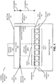
- FIG. 1 presents a block diagram of a hybrid integrated module 100.
- This hybrid integrated module includes: a semiconductor die 110 having a top surface 112, which may include electronic circuits in a dielectric stack; an adhesive 114 (such as epoxy) mechanically coupled to top surface 112 of semiconductor die 110; and an integrated device 116.
- integrated device 116 includes: a semiconductor layer 118 having a top surface 120, a bottom surface 122 and a thickness 124, where top surface 120 is mechanically coupled to adhesive 114, so that semiconductor layer 118 and semiconductor die 110 are mounted face-to-face; an oxide layer 126 having a top surface 128 (which is slightly offset from bottom surface 122 for clarity), a bottom surface 130 and a thickness 132, where top surface 128 is disposed on bottom surface 122; and an optical device 134 disposed on bottom surface 130.
- semiconductor layer 118 includes an optical waveguide 136-1 that conveys an optical signal (such as a wavelength-division-multiplexing signal), and the materials and/or geometry of integrated device 116 (such as thicknesses 124 and 132) may be selected and/or defined so that the optical signal is evanescently coupled between optical waveguide 136-1 and optical device 134 ( i.e., a spatial extent of an optical mode associated with the optical signal may extend through thickness 132 to bottom surface 130).
- thickness 124 of semiconductor layer 118 may be between 0.1 and 4 ⁇ m and thickness 132 of oxide layer 126 may be less than 0.5 ⁇ m (such as 0.1 ⁇ m).
- the evanescent coupling may be achieved by using a thin oxide layer with a thick silicon layer or a thin silicon layer (the lower bound being approximately one-half of the diffraction limit of the optical signal).
- a thin oxide layer with a thick silicon layer or a thin silicon layer the lower bound being approximately one-half of the diffraction limit of the optical signal.
- the electrical functions in hybrid integrated module 100 have been physically separated from the optical functions, these functions can be independently optimized. This may facilitate monolithic integration of photonic circuits and electronic circuits without the photonic circuits imposing constraints on thicknesses 124 and 132.
- thickness 132 can be reproducibly controlled to better than 1% accuracy, the evanescent coupling can be implemented in a very controlled and accurate manner with minimal optical loss.
- hybrid integrated module 100 may provide additional design degrees of freedom.
- optical device 134 may include: an optical modulator, an optical switch, an optical source, an optical waveguide, a wavelength-selective element or filter, a light-detecting element, etc.
- optical device 134 may include materials that are not compatible with standard CMOS processing, such as: III-V semiconductors ( e.g. , a silicon-germanium alloy), an electro-optic material, a liquid crystal and/or a ferroelectric material.
- the materials on bottom surface 130 may be defined or deposited during post-processing of integrated device 116 at the chip or wafer level (for example, optical device 134 may be deposited or bonded onto oxide layer 126 after front-end-of-line processing is completed in a back-end-of-line complaint process).
- the mechanical coupling provided by adhesive 114 includes solder balls, such as solder ball 138 (e.g ., bondline micro-bumps or micro-solder), electrically coupling pads 140-1 on top surface 112 and pads 140-2 on top surface 120, where adhesive 114 at least in part fills a space between top surface 112 and top surface 120 ( i.e., there may be underfill).
- solder ball 138 e.g ., bondline micro-bumps or micro-solder
- electrically coupling pads 140-1 on top surface 112 and pads 140-2 on top surface 120 where adhesive 114 at least in part fills a space between top surface 112 and top surface 120 ( i.e., there may be underfill).
- integrated device 116 may be mechanically coupled to semiconductor die 110 using a flip-chip technique.
- semiconductor layer 118 may include silicon
- oxide layer 126 may include a dielectric or an oxide, such as silicon dioxide.
- semiconductor layer 118 and oxide layer 126 may comprise a silicon-on-insulator ( SOI ) technology in which the semiconductor die on top of oxide layer 126 (such as the silicon-handler substrate) has been removed, for example, by mechanical polish and/or etching.
- SOI silicon-on-insulator
- optical losses associated with the evanescent coupling of the optical signal through oxide layer 126 into the silicon-handler substrate may be eliminated.
- optical device 134 may be faster, smaller and more power-efficient relative to existing optical components that are implemented using SOI technology.
- semiconductor die 110 may include electronic circuits implemented in silicon, such as: a VLSI chip that provides power, and serves as a mechanical handler and/or an electrical driver; a processor; a radio-frequency circuit; memory; a mixed-signal circuit; and/or a digital circuit.
- optical device 134 may include a wide variety of optical components and/or materials.
- optical device 134 statically or dynamically modulates the optical signal.
- optical device 134 may include an optical modulator. This optical modulator may correct variations in an actual resonance wavelength of the ring resonator from a target resonance wavelength because of process variability and manufacturing tolerances, as well as variations in thickness 124.
- FIGs. 2A and 2B present block diagrams of ring resonators 210 and 260, respectively, in hybrid integrated module 100 ( FIG. 1 ). These ring resonators may be fabricated on bottom surface 130 immediately above optical waveguide 136-1. Moreover, ring resonators 210 and 260 may be used to modify the index of refraction of the cladding of optical waveguide 136-1 and, thus, to change the optical-waveguide ring-propagation constant of optical waveguide 136-1. For example, an electric voltage may be applied to electrodes 212 or 262 to generate an electric field in a horizontal ( FIG. 2A ) or a vertical direction ( FIG.
- optical device 134 may electronically tailor the optical mode of the optical signal via the evanescent tail.
- electro-optic material such as a ferroelectric material, e.g., barium strontium titanate, lead zirconium titanate or a liquid crystal
- electro-absorber material such as germanium
- the optical device may have far lower power requirements than thermally tuning, even when it is tuned across the entire free-spectral range of ring resonator 210 or 260.
- the power consumption may be an order of magnitude smaller (e.g., microWatts instead of milliWatts).
- electrodes 212 and 262 in ring resonators 210 and 260 may be electrically coupled to semiconductor layer 118 and/or semiconductor die 110 in FIG. 1 ( e.g., using through silicon vias).
- the optical device includes another optical waveguide that conveys the optical signal across reticle boundaries in the integrated device. This is shown in FIG. 3 , which presents a block diagram of a hybrid integrated module 300.
- integrated device 116 may function as a 'bridge chip' that optically couples optical signal 310 to multiple chips on a common wafer.
- optical device 134 may include an optical source that provides the optical signal.
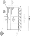
- FIG. 4 presents a block diagram of a hybrid integrated module 400.
- a III-V semiconductor laser 410 may be bonded on top of bottom surface 130. This laser may be aligned with and situated on top of optical waveguide 136-1.
- optical signal 412 output by this laser may be evanescently coupled to optical waveguide 136-1 through oxide layer 126 ( FIG. 1 ).
- laser 410 and/or optical waveguide 136-1 may be terminated with appropriately sized tapers to relax the x - and y - alignment tolerances, as well as to accommodate for an optical-mode mismatch between an optical waveguide in optical device 134 ( FIG. 1 ) and optical waveguide 136-1.
- the efficiency of the evanescent coupling between two adjacent optical waveguides is dependent on the accuracy of the spacing between them. In these embodiments, this spacing is set by thickness 132 in FIG. 1 (which is routinely specified at under 1% in a typical SOI wafer). Such tight thickness tolerance can facilitate optical coupling with low optical loss from laser 410 to optical waveguide 136-1.
- the photonic circuits may be completed, along with the necessary dielectric and metal inter-connect layering, and may even be monolithically integrated with electronic circuits, before integration of laser 410.
- oxide layer 126 is expected to be flat once exposed ( e.g., after the silicon substrate-handler is removed) and may not need polishing for planarization. Note that, if needed, through-silicon vias can be placed in oxide layer 126 to connect the front-side circuits to the electrical contacts of laser 410 so that optical device 134 ( FIG. 1 ) can be electronically controlled and stimulated using the front-side circuits.
- the hybrid integrated module may facilitate 3-dimensional integration of additional integrated devices and/or additional hybrid integrated modules, thereby scaling up the component density and facilitating a variety of architectures and applications.
- one or more additional integrated devices may be stacked on top of integrated device 116 such that the top surface of a semiconductor layer in one of the additional integrated devices faces bottom surface 130 of oxide layer 126 in integrated device 116.
- one or more additional hybrid integrated modules may be positioned so that optical devices (such as optical device 134) face each other in a multi-chip module ( MCM ) .
- MCM multi-chip module
- optical couplers such as diffraction grating couplers or mirrors
- semiconductor layer 118 and/or on bottom surface 130 may be defined in semiconductor layer 118 and/or on bottom surface 130 to provide optical coupling to the additional integrated devices and/or the additional hybrid integrated modules.
- optical device 134 may be used to convey the optical signal across the reticle line (i.e., optical device 134 may function as a 'bridge chip').
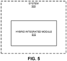
- FIG. 5 presents a block diagram illustrating a system 500 that includes hybrid integrated module 510.
- the hybrid integrated module and/or the MCM may be used in a variety of applications, including: VLSI circuits, communication systems (such as WDM ) , storage area networks, data centers, networks (such as local area networks), and/or computer systems (such as multiple-core processor computer systems).
- system 500 may include, but is not limited to: a server, a laptop computer, a communication device or system, a personal computer, a tablet computer, a work station, a mainframe computer, a blade, an enterprise computer, a data center, a portable-computing device, a supercomputer, a network-attached-storage ( NAS ) system, a storage-area-network (SAN ) system, and/or another electronic computing device.
- NAS network-attached-storage
- SAN storage-area-network
- a given computer system may be at one location or may be distributed over multiple, geographically dispersed locations.
- the preceding embodiments of the hybrid integrated module, the MCM, and/or system 500 may include fewer components or additional components.
- semiconductor layer 118 in FIG. 1 may include poly-silicon or amorphous silicon.
- optical device 134 i.e., where evanescent coupling is desired.
- a wide variety of fabrication techniques may be used to fabricate the hybrid integrated module in the preceding embodiments, as is known to one of skill in the art.
- optical components may be used in or in conjunction with the hybrid integrated module.
- optical device 134 in FIG. 1 is thermally and/or electrically tuned. Furthermore, while inclusion of optical device 134 in integrated device 116 has been used as an illustrative example, in other embodiments the hybrid integrated module does not include an optical device.
- FIG. 6 presents a flow chart illustrating a method 600 for fabricating the hybrid integrated module.
- an adhesive is applied to a top surface of a semiconductor die (operation 610).
- an integrated device is placed on the adhesive (operation 612).
- the integrated device includes: a semiconductor layer having a top surface, a bottom surface and a thickness, where the top surface of the semiconductor layer is mechanically coupled to the adhesive, and where the semiconductor layer includes an optical waveguide configured to convey an optical signal; an oxide layer having a top surface, a bottom surface and a thickness, which is disposed on the bottom surface of the semiconductor layer; and an optical device disposed on the bottom surface of the oxide layer.
- the thickness of the semiconductor layer and/or the thickness of the oxide layer may be defined so that the optical signal is evanescently coupled between the optical waveguide and the optical device.
- method 600 there may be additional or fewer operations. Moreover, the order of the operations may be changed, and/or two or more operations may be combined into a single operation.
Landscapes
- Physics & Mathematics (AREA)
- General Physics & Mathematics (AREA)
- Optics & Photonics (AREA)
- Engineering & Computer Science (AREA)
- Microelectronics & Electronic Packaging (AREA)
- Optical Integrated Circuits (AREA)
- Optical Modulation, Optical Deflection, Nonlinear Optics, Optical Demodulation, Optical Logic Elements (AREA)
- Semiconductor Lasers (AREA)
- Optical Couplings Of Light Guides (AREA)
Claims (14)
- Hybrides integriertes Modul (100), umfassend:einen Halbleiterchip (110) mit einer Oberseite (112) ;einen Klebstoff (114), der mechanisch an die Oberseite des Halbleiterchips gekoppelt ist; undeine integrierte Vorrichtung (116), wobei die integrierte Vorrichtung einschließt:eine Halbleiterschicht (118) mit einer Oberseite (120), einer Unterseite (122) und einer Dicke (124), wobei die Oberseite der Halbleiterschicht mechanisch an den Klebstoff gekoppelt ist, und wobei die Halbleiterschicht einen optischen Wellenleiter (136-1) einschließt, der ausgestaltet ist, um ein optisches Signal zu transportieren;Kopplungskontaktstellen (140-1), die auf der Oberseite (112) des Halbleiterchips (110) angeordnet sind;Kopplungskontaktstellen (140-2), die auf der Oberseite (120) der Halbleiterschicht (118) angeordnet sind;Lotperlen (138), die die Kontaktstellen (140-1) auf der Oberseite des Halbleiterchips und die Kontaktstellen (140-2) auf der Oberseite der Halbleiterschicht elektrisch koppeln, wobei der Klebstoff (114) mindestens teilweise einen Raum zwischen der Oberseite des Halbleiterchips und der Oberseite der Halbleiterschicht füllt;eine Oxidschicht (126) mit einer Oberseite (128), einer Unterseite (130) und einer Dicke (132), wobei die Oberseite der Oxidschicht auf der Unterseite der Halbleiterschicht angeordnet ist; undeine optische Vorrichtung (134), die auf der Unterseite der Oxidschicht (126) angeordnet ist, wobeidie Dicke der Halbleiterschicht und die Dicke der Oxidschicht so definiert sind, dass das optische Signal nichtausbreitungsfähig zwischen dem optischen Wellenleiter (136-1) und der optischen Vorrichtung (134) gekoppelt ist.
- Hybrides integriertes Modul nach Anspruch 1, wobei die Halbleiterschicht einen Ringresonator einschließt und die optische Vorrichtung das Abstimmen des Ringresonators erleichtert, mit einem Leistungsverbrauch, der unter demjenigen liegt, der mit thermischem Abstimmen verbunden ist.
- Hybrides integriertes Modul nach Anspruch 2, wobei die optische Vorrichtung ausgestaltet ist, um Schwankungen in einer tatsächlichen Resonanzwellenlänge des Ringresonators zu einer Zielresonanzwellenlänge zu korrigieren.
- Hybrides integriertes Modul nach einem der vorhergehenden Ansprüche, wobei die optische Vorrichtung einen weiteren optischen Wellenleiter einschließt, der auf der Unterseite der Oxidschicht angeordnet ist; und
wobei der weitere optische Wellenleiter ausgestaltet ist, um das optische Signal über Fadenkreuzgrenzen hinweg in der integrierten Vorrichtung zu transportieren. - Hybrides integriertes Modul nach einem der vorhergehenden Ansprüche, wobei die optische Vorrichtung eine optische Quelle einschließt, die auf der Unterseite der Oxidschicht angeordnet ist; und
wobei die optische Quelle ausgestaltet ist, um das optische Signal bereitzustellen. - Hybrides integriertes Modul nach einem der vorhergehenden Ansprüche, wobei die Dicke der Halbleiterschicht zwischen 0,1 und 4 µm liegt.
- Hybrides integriertes Modul nach einem der vorhergehenden Ansprüche, wobei die Dicke der Halbleiterschicht kleiner als 0,5 µm ist.
- Hybrides integriertes Modul nach einem der vorhergehenden Ansprüche, wobei die integrierte Vorrichtung unter Verwendung einer Flip-Chip-Technik mechanisch an den Halbleiterchip gekoppelt ist.
- Hybrides integriertes Modul nach einem der vorhergehenden Ansprüche, wobei die Halbleiterschicht Silicium einschließt und die Oxidschicht Siliciumdioxid einschließt.
- Hybrides integriertes Modul nach einem der vorhergehenden Ansprüche, wobei die Halbleiterschicht und die Oxidschicht eine Silicium-auf-Isolator-Technologie umfassen, bei der ein zweiter Halbleiterchip oben auf der Oxidschicht entfernt worden ist.
- Hybrides integriertes Modul nach einem der vorhergehenden Ansprüche, wobei die optische Vorrichtung ausgestaltet ist, um mindestens eine der folgenden Funktionen durchzuführen:Modulieren des optischen Signals;dynamisches Modulieren des optischen Signals;Schalten des optischen Signals.
- Hybrides integriertes Modul nach einem der vorhergehenden Ansprüche, wobei die optische Vorrichtung eines von einem elektrooptischen Material, einem Flüssigkristall und einem ferroelektrischen Material einschließt.
- System, umfassend:das hybride integrierte Modul nach einem der vorhergehenden Ansprüche;einen Prozessor, der in eine (n) von dem Halbleiterchip und der integrierten Vorrichtung eingebaut ist; undeinen Speicher, der in eine(n) von dem Halbleiterchip und der integrierten Vorrichtung eingebaut ist.
- Verfahren zum Fertigen eines hybriden integrierten Moduls (100) gemäß Anspruch 1, wobei das Verfahren umfasst:Aufbringen eines Klebstoffs auf eine Oberseite eines Halbleiterchips; undPlatzieren einer integrierten Vorrichtung auf dem Klebstoff, wobei die integrierte Vorrichtung einschließt:eine Halbleiterschicht mit einer Oberseite, einer Unterseite und einer Dicke, wobei die Oberseite der Halbleiterschicht mechanisch an den Klebstoff gekoppelt ist; undwobei die Halbleiterschicht einen optischen Wellenleiter einschließt, der zum Transportieren eines optischen Signals ausgestaltet ist, wobei Kontaktstellen auf der Oberseite des Halbleiterchips und Kontaktstellen auf der Oberseite der Halbleiterschicht elektrisch durch Lotperlen gekoppelt sind, und wobei der Klebstoff mindestens teilweise einen Raum zwischen der Oberseite des Halbleiterchips und der Oberseite der Halbleiterschicht füllt;eine Oxidschicht mit einer Oberseite, einer Unterseite und einer Dicke, wobei die Oberseite der Oxidschicht auf der Unterseite der Halbleiterschicht angeordnet ist; undeine optische Vorrichtung, die auf der Unterseite der Oxidschicht angeordnet ist, wobei die Dicke der Halbleiterschicht und die Dicke der Oxidschicht so definiert sind, dass das optische Signal nichtausbreitungsfähig zwischen dem optischen Wellenleiter und der optischen Vorrichtung gekoppelt ist.
Applications Claiming Priority (2)
| Application Number | Priority Date | Filing Date | Title |
|---|---|---|---|
| US13/331,767 US8428404B1 (en) | 2011-12-20 | 2011-12-20 | Optical device on inverted, substrateless chip |
| PCT/US2012/066536 WO2013095866A1 (en) | 2011-12-20 | 2012-11-26 | Optical device on inverted, substrateless chip |
Publications (2)
| Publication Number | Publication Date |
|---|---|
| EP2795381A1 EP2795381A1 (de) | 2014-10-29 |
| EP2795381B1 true EP2795381B1 (de) | 2019-05-08 |
Family
ID=47505293
Family Applications (1)
| Application Number | Title | Priority Date | Filing Date |
|---|---|---|---|
| EP12810445.2A Active EP2795381B1 (de) | 2011-12-20 | 2012-11-26 | Ein hybrides integriertes Modul mit einem optischen Gerät |
Country Status (6)
| Country | Link |
|---|---|
| US (1) | US8428404B1 (de) |
| EP (1) | EP2795381B1 (de) |
| JP (1) | JP6234374B2 (de) |
| CN (1) | CN103975262B (de) |
| TW (1) | TWI585477B (de) |
| WO (1) | WO2013095866A1 (de) |
Families Citing this family (14)
| Publication number | Priority date | Publication date | Assignee | Title |
|---|---|---|---|---|
| US8796811B2 (en) * | 2011-08-09 | 2014-08-05 | Oracle International Corporation | Hybrid substrateless device with enhanced tuning efficiency |
| US9891383B2 (en) | 2014-06-26 | 2018-02-13 | Alcatel Lucent | Monolithic silicon lasers |
| US10096971B2 (en) | 2014-06-26 | 2018-10-09 | Alcatel-Lucent Usa Inc. | Hybrid semiconductor lasers |
| US9442314B2 (en) * | 2014-08-12 | 2016-09-13 | Oracle International Corporation | Ferroelectric-enhanced tuning of ring resonators by using fields parallel to and above a top surface thereof |
| US9772463B2 (en) | 2014-09-04 | 2017-09-26 | International Business Machines Corporation | Intra chip optical interconnect structure |
| TWI624705B (zh) * | 2015-03-12 | 2018-05-21 | 山姆科技公司 | 包含矽光晶片和耦合器晶片的光學模組 |
| US9678273B2 (en) | 2015-06-01 | 2017-06-13 | International Business Machines Corporation | Device for propagating light and method for fabricating a device |
| US9658400B2 (en) | 2015-06-01 | 2017-05-23 | International Business Machines Corporation | Method for fabricating a device for propagating light |
| JP6933794B2 (ja) * | 2016-12-01 | 2021-09-08 | 富士通株式会社 | 光モジュール及び光モジュールの製造方法 |
| US11409063B2 (en) * | 2018-02-05 | 2022-08-09 | Samtec, Inc. | Optical interposer |
| JP7454687B2 (ja) | 2020-01-29 | 2024-03-22 | サイカンタム・コーポレーション | デバイスおよび光スイッチ |
| US12461398B2 (en) * | 2020-03-03 | 2025-11-04 | Psiquantum, Corp. | Phase shifter employing electro-optic material sandwich |
| US20210064958A1 (en) * | 2020-11-17 | 2021-03-04 | Intel Corporation | Heterogeneously integrated optical neural network accelerator |
| CN115016153A (zh) * | 2022-07-08 | 2022-09-06 | 桂林电子科技大学 | 一种可重构的定向耦合器 |
Citations (1)
| Publication number | Priority date | Publication date | Assignee | Title |
|---|---|---|---|---|
| EP1020748A1 (de) * | 1997-10-01 | 2000-07-19 | Hitachi Chemical Company, Ltd. | Optischer signalprozessor |
Family Cites Families (11)
| Publication number | Priority date | Publication date | Assignee | Title |
|---|---|---|---|---|
| JP2004177974A (ja) * | 1997-10-01 | 2004-06-24 | Hitachi Chem Co Ltd | 光情報処理装置 |
| EP1402564B1 (de) * | 2001-05-17 | 2017-07-12 | Cisco Technology, Inc. | Integrierte optische/elektronische schaltungen und zugeordnete verfahren zur gleichzeitigen erzeugung dieser |
| US7218799B2 (en) * | 2005-03-29 | 2007-05-15 | Analog Devices, Inc. | External optical modulator |
| US7528403B1 (en) * | 2005-04-25 | 2009-05-05 | California Institute Of Technology | Hybrid silicon-on-insulator waveguide devices |
| US7257283B1 (en) * | 2006-06-30 | 2007-08-14 | Intel Corporation | Transmitter-receiver with integrated modulator array and hybrid bonded multi-wavelength laser array |
| EP1939955A3 (de) * | 2006-12-27 | 2015-12-23 | CSEM Centre Suisse d'Electronique et de Microtechnique SA - Recherche et Développement | Optische Vorrichtung sowie System und Verfahren zur Herstellung der Vorrichtung |
| US7764852B2 (en) * | 2007-07-30 | 2010-07-27 | Hewlett-Packard Development Company, L.P. | Microresonantor systems and methods of fabricating the same |
| US8483524B2 (en) * | 2008-08-14 | 2013-07-09 | Gigoptix, Inc. | Integrated electro-optic device and method of making |
| WO2009063942A1 (ja) * | 2007-11-16 | 2009-05-22 | Nec Corporation | 光導波路 |
| US8260151B2 (en) * | 2008-04-18 | 2012-09-04 | Freescale Semiconductor, Inc. | Optical communication integration |
| TW201123353A (en) * | 2009-12-29 | 2011-07-01 | United Microelectronics Corp | Structure of a semiconductor device having a waveguide and method of forming the same |
-
2011
- 2011-12-20 US US13/331,767 patent/US8428404B1/en active Active
-
2012
- 2012-11-23 TW TW101144002A patent/TWI585477B/zh active
- 2012-11-26 JP JP2014549069A patent/JP6234374B2/ja active Active
- 2012-11-26 WO PCT/US2012/066536 patent/WO2013095866A1/en not_active Ceased
- 2012-11-26 EP EP12810445.2A patent/EP2795381B1/de active Active
- 2012-11-26 CN CN201280059786.3A patent/CN103975262B/zh active Active
Patent Citations (1)
| Publication number | Priority date | Publication date | Assignee | Title |
|---|---|---|---|---|
| EP1020748A1 (de) * | 1997-10-01 | 2000-07-19 | Hitachi Chemical Company, Ltd. | Optischer signalprozessor |
Also Published As
| Publication number | Publication date |
|---|---|
| EP2795381A1 (de) | 2014-10-29 |
| US8428404B1 (en) | 2013-04-23 |
| CN103975262B (zh) | 2018-01-23 |
| CN103975262A (zh) | 2014-08-06 |
| TWI585477B (zh) | 2017-06-01 |
| JP2015506488A (ja) | 2015-03-02 |
| JP6234374B2 (ja) | 2017-11-22 |
| TW201337363A (zh) | 2013-09-16 |
| WO2013095866A1 (en) | 2013-06-27 |
Similar Documents
| Publication | Publication Date | Title |
|---|---|---|
| EP2795381B1 (de) | Ein hybrides integriertes Modul mit einem optischen Gerät | |
| US8796811B2 (en) | Hybrid substrateless device with enhanced tuning efficiency | |
| US11841531B2 (en) | Wafer scale bonded active photonics interposer | |
| US20220342164A1 (en) | Integrated circuit device and method | |
| EP3159721B1 (de) | Verfahren und system für eine chip-auf-wafer-auf-substrat-anordnung | |
| US9829626B2 (en) | Hybrid-integrated multi-chip module | |
| US8768123B2 (en) | Three-dimensional macro-chip including optical interconnects | |
| US9696486B2 (en) | Surface-normal coupler for silicon-on-insulator platforms | |
| US20060177173A1 (en) | Vertical stacking of multiple integrated circuits including SOI-based optical components | |
| US20130181233A1 (en) | Silicon photonics wafer using standard silicon-on-insulator processes through substrate removal or transfer | |
| EP3335063A1 (de) | Selbstangeordnetes vertikal ausgerichtetes mehrchipmodul | |
| US10649138B2 (en) | Optical device having a photonic chip with one or more suspended functional portions | |
| EP4645614A1 (de) | Integrationsverfahren für modulare heterogene optoelektronische integrationsarchitektur auf siliciumbasis | |
| US20110069925A1 (en) | Macro-chip including a surface-normal device | |
| EP4109152A1 (de) | Gerät und verfahren zur herstellung einer vertikal zerlegten photonischen vorrichtung | |
| US10605985B2 (en) | Integration of bonded optoelectronics, photonics waveguide and VLSI SOI | |
| CN222354102U (zh) | 光学装置 | |
| US20250291136A1 (en) | System and methods for integrated epic architecture | |
| US20250284074A1 (en) | System and methods for co-package optics package architecture | |
| US11774689B2 (en) | Photonics chips and semiconductor products having angled optical fibers | |
| JP7688294B2 (ja) | 光モジュールおよびその作製方法 | |
| CN121832134A (zh) | 一种背面异质集成光芯片及其制备方法 |
Legal Events
| Date | Code | Title | Description |
|---|---|---|---|
| PUAI | Public reference made under article 153(3) epc to a published international application that has entered the european phase |
Free format text: ORIGINAL CODE: 0009012 |
|
| 17P | Request for examination filed |
Effective date: 20140717 |
|
| AK | Designated contracting states |
Kind code of ref document: A1 Designated state(s): AL AT BE BG CH CY CZ DE DK EE ES FI FR GB GR HR HU IE IS IT LI LT LU LV MC MK MT NL NO PL PT RO RS SE SI SK SM TR |
|
| DAX | Request for extension of the european patent (deleted) | ||
| GRAP | Despatch of communication of intention to grant a patent |
Free format text: ORIGINAL CODE: EPIDOSNIGR1 |
|
| STAA | Information on the status of an ep patent application or granted ep patent |
Free format text: STATUS: GRANT OF PATENT IS INTENDED |
|
| INTG | Intention to grant announced |
Effective date: 20180713 |
|
| RIN1 | Information on inventor provided before grant (corrected) |
Inventor name: SHUBIN, IVAN Inventor name: CUNNINGHAM, JOHN E. Inventor name: KRISHNAMOORTHY, ASHOK V. |
|
| GRAJ | Information related to disapproval of communication of intention to grant by the applicant or resumption of examination proceedings by the epo deleted |
Free format text: ORIGINAL CODE: EPIDOSDIGR1 |
|
| STAA | Information on the status of an ep patent application or granted ep patent |
Free format text: STATUS: REQUEST FOR EXAMINATION WAS MADE |
|
| INTC | Intention to grant announced (deleted) | ||
| GRAS | Grant fee paid |
Free format text: ORIGINAL CODE: EPIDOSNIGR3 |
|
| STAA | Information on the status of an ep patent application or granted ep patent |
Free format text: STATUS: GRANT OF PATENT IS INTENDED |
|
| GRAP | Despatch of communication of intention to grant a patent |
Free format text: ORIGINAL CODE: EPIDOSNIGR1 |
|
| INTG | Intention to grant announced |
Effective date: 20190107 |
|
| GRAA | (expected) grant |
Free format text: ORIGINAL CODE: 0009210 |
|
| STAA | Information on the status of an ep patent application or granted ep patent |
Free format text: STATUS: THE PATENT HAS BEEN GRANTED |
|
| AK | Designated contracting states |
Kind code of ref document: B1 Designated state(s): AL AT BE BG CH CY CZ DE DK EE ES FI FR GB GR HR HU IE IS IT LI LT LU LV MC MK MT NL NO PL PT RO RS SE SI SK SM TR |
|
| REG | Reference to a national code |
Ref country code: GB Ref legal event code: FG4D |
|
| REG | Reference to a national code |
Ref country code: CH Ref legal event code: EP Ref country code: AT Ref legal event code: REF Ref document number: 1131075 Country of ref document: AT Kind code of ref document: T Effective date: 20190515 |
|
| REG | Reference to a national code |
Ref country code: IE Ref legal event code: FG4D |
|
| REG | Reference to a national code |
Ref country code: DE Ref legal event code: R096 Ref document number: 602012059959 Country of ref document: DE |
|
| REG | Reference to a national code |
Ref country code: NL Ref legal event code: MP Effective date: 20190508 |
|
| REG | Reference to a national code |
Ref country code: LT Ref legal event code: MG4D |
|
| PG25 | Lapsed in a contracting state [announced via postgrant information from national office to epo] |
Ref country code: HR Free format text: LAPSE BECAUSE OF FAILURE TO SUBMIT A TRANSLATION OF THE DESCRIPTION OR TO PAY THE FEE WITHIN THE PRESCRIBED TIME-LIMIT Effective date: 20190508 Ref country code: NO Free format text: LAPSE BECAUSE OF FAILURE TO SUBMIT A TRANSLATION OF THE DESCRIPTION OR TO PAY THE FEE WITHIN THE PRESCRIBED TIME-LIMIT Effective date: 20190808 Ref country code: NL Free format text: LAPSE BECAUSE OF FAILURE TO SUBMIT A TRANSLATION OF THE DESCRIPTION OR TO PAY THE FEE WITHIN THE PRESCRIBED TIME-LIMIT Effective date: 20190508 Ref country code: LT Free format text: LAPSE BECAUSE OF FAILURE TO SUBMIT A TRANSLATION OF THE DESCRIPTION OR TO PAY THE FEE WITHIN THE PRESCRIBED TIME-LIMIT Effective date: 20190508 Ref country code: ES Free format text: LAPSE BECAUSE OF FAILURE TO SUBMIT A TRANSLATION OF THE DESCRIPTION OR TO PAY THE FEE WITHIN THE PRESCRIBED TIME-LIMIT Effective date: 20190508 Ref country code: AL Free format text: LAPSE BECAUSE OF FAILURE TO SUBMIT A TRANSLATION OF THE DESCRIPTION OR TO PAY THE FEE WITHIN THE PRESCRIBED TIME-LIMIT Effective date: 20190508 Ref country code: PT Free format text: LAPSE BECAUSE OF FAILURE TO SUBMIT A TRANSLATION OF THE DESCRIPTION OR TO PAY THE FEE WITHIN THE PRESCRIBED TIME-LIMIT Effective date: 20190908 Ref country code: SE Free format text: LAPSE BECAUSE OF FAILURE TO SUBMIT A TRANSLATION OF THE DESCRIPTION OR TO PAY THE FEE WITHIN THE PRESCRIBED TIME-LIMIT Effective date: 20190508 Ref country code: FI Free format text: LAPSE BECAUSE OF FAILURE TO SUBMIT A TRANSLATION OF THE DESCRIPTION OR TO PAY THE FEE WITHIN THE PRESCRIBED TIME-LIMIT Effective date: 20190508 |
|
| PG25 | Lapsed in a contracting state [announced via postgrant information from national office to epo] |
Ref country code: BG Free format text: LAPSE BECAUSE OF FAILURE TO SUBMIT A TRANSLATION OF THE DESCRIPTION OR TO PAY THE FEE WITHIN THE PRESCRIBED TIME-LIMIT Effective date: 20190808 Ref country code: GR Free format text: LAPSE BECAUSE OF FAILURE TO SUBMIT A TRANSLATION OF THE DESCRIPTION OR TO PAY THE FEE WITHIN THE PRESCRIBED TIME-LIMIT Effective date: 20190809 Ref country code: LV Free format text: LAPSE BECAUSE OF FAILURE TO SUBMIT A TRANSLATION OF THE DESCRIPTION OR TO PAY THE FEE WITHIN THE PRESCRIBED TIME-LIMIT Effective date: 20190508 Ref country code: RS Free format text: LAPSE BECAUSE OF FAILURE TO SUBMIT A TRANSLATION OF THE DESCRIPTION OR TO PAY THE FEE WITHIN THE PRESCRIBED TIME-LIMIT Effective date: 20190508 |
|
| REG | Reference to a national code |
Ref country code: AT Ref legal event code: MK05 Ref document number: 1131075 Country of ref document: AT Kind code of ref document: T Effective date: 20190508 |
|
| PG25 | Lapsed in a contracting state [announced via postgrant information from national office to epo] |
Ref country code: SK Free format text: LAPSE BECAUSE OF FAILURE TO SUBMIT A TRANSLATION OF THE DESCRIPTION OR TO PAY THE FEE WITHIN THE PRESCRIBED TIME-LIMIT Effective date: 20190508 Ref country code: DK Free format text: LAPSE BECAUSE OF FAILURE TO SUBMIT A TRANSLATION OF THE DESCRIPTION OR TO PAY THE FEE WITHIN THE PRESCRIBED TIME-LIMIT Effective date: 20190508 Ref country code: CZ Free format text: LAPSE BECAUSE OF FAILURE TO SUBMIT A TRANSLATION OF THE DESCRIPTION OR TO PAY THE FEE WITHIN THE PRESCRIBED TIME-LIMIT Effective date: 20190508 Ref country code: RO Free format text: LAPSE BECAUSE OF FAILURE TO SUBMIT A TRANSLATION OF THE DESCRIPTION OR TO PAY THE FEE WITHIN THE PRESCRIBED TIME-LIMIT Effective date: 20190508 Ref country code: EE Free format text: LAPSE BECAUSE OF FAILURE TO SUBMIT A TRANSLATION OF THE DESCRIPTION OR TO PAY THE FEE WITHIN THE PRESCRIBED TIME-LIMIT Effective date: 20190508 Ref country code: AT Free format text: LAPSE BECAUSE OF FAILURE TO SUBMIT A TRANSLATION OF THE DESCRIPTION OR TO PAY THE FEE WITHIN THE PRESCRIBED TIME-LIMIT Effective date: 20190508 |
|
| REG | Reference to a national code |
Ref country code: DE Ref legal event code: R097 Ref document number: 602012059959 Country of ref document: DE |
|
| PG25 | Lapsed in a contracting state [announced via postgrant information from national office to epo] |
Ref country code: SM Free format text: LAPSE BECAUSE OF FAILURE TO SUBMIT A TRANSLATION OF THE DESCRIPTION OR TO PAY THE FEE WITHIN THE PRESCRIBED TIME-LIMIT Effective date: 20190508 Ref country code: IT Free format text: LAPSE BECAUSE OF FAILURE TO SUBMIT A TRANSLATION OF THE DESCRIPTION OR TO PAY THE FEE WITHIN THE PRESCRIBED TIME-LIMIT Effective date: 20190508 |
|
| PLBE | No opposition filed within time limit |
Free format text: ORIGINAL CODE: 0009261 |
|
| STAA | Information on the status of an ep patent application or granted ep patent |
Free format text: STATUS: NO OPPOSITION FILED WITHIN TIME LIMIT |
|
| PG25 | Lapsed in a contracting state [announced via postgrant information from national office to epo] |
Ref country code: TR Free format text: LAPSE BECAUSE OF FAILURE TO SUBMIT A TRANSLATION OF THE DESCRIPTION OR TO PAY THE FEE WITHIN THE PRESCRIBED TIME-LIMIT Effective date: 20190508 |
|
| 26N | No opposition filed |
Effective date: 20200211 |
|
| PG25 | Lapsed in a contracting state [announced via postgrant information from national office to epo] |
Ref country code: PL Free format text: LAPSE BECAUSE OF FAILURE TO SUBMIT A TRANSLATION OF THE DESCRIPTION OR TO PAY THE FEE WITHIN THE PRESCRIBED TIME-LIMIT Effective date: 20190508 |
|
| PG25 | Lapsed in a contracting state [announced via postgrant information from national office to epo] |
Ref country code: SI Free format text: LAPSE BECAUSE OF FAILURE TO SUBMIT A TRANSLATION OF THE DESCRIPTION OR TO PAY THE FEE WITHIN THE PRESCRIBED TIME-LIMIT Effective date: 20190508 |
|
| REG | Reference to a national code |
Ref country code: CH Ref legal event code: PL |
|
| PG25 | Lapsed in a contracting state [announced via postgrant information from national office to epo] |
Ref country code: MC Free format text: LAPSE BECAUSE OF FAILURE TO SUBMIT A TRANSLATION OF THE DESCRIPTION OR TO PAY THE FEE WITHIN THE PRESCRIBED TIME-LIMIT Effective date: 20190508 Ref country code: LU Free format text: LAPSE BECAUSE OF NON-PAYMENT OF DUE FEES Effective date: 20191126 Ref country code: LI Free format text: LAPSE BECAUSE OF NON-PAYMENT OF DUE FEES Effective date: 20191130 Ref country code: CH Free format text: LAPSE BECAUSE OF NON-PAYMENT OF DUE FEES Effective date: 20191130 |
|
| REG | Reference to a national code |
Ref country code: BE Ref legal event code: MM Effective date: 20191130 |
|
| PG25 | Lapsed in a contracting state [announced via postgrant information from national office to epo] |
Ref country code: IE Free format text: LAPSE BECAUSE OF NON-PAYMENT OF DUE FEES Effective date: 20191126 Ref country code: FR Free format text: LAPSE BECAUSE OF NON-PAYMENT OF DUE FEES Effective date: 20191130 |
|
| PG25 | Lapsed in a contracting state [announced via postgrant information from national office to epo] |
Ref country code: BE Free format text: LAPSE BECAUSE OF NON-PAYMENT OF DUE FEES Effective date: 20191130 |
|
| PG25 | Lapsed in a contracting state [announced via postgrant information from national office to epo] |
Ref country code: CY Free format text: LAPSE BECAUSE OF FAILURE TO SUBMIT A TRANSLATION OF THE DESCRIPTION OR TO PAY THE FEE WITHIN THE PRESCRIBED TIME-LIMIT Effective date: 20190508 |
|
| PG25 | Lapsed in a contracting state [announced via postgrant information from national office to epo] |
Ref country code: IS Free format text: LAPSE BECAUSE OF FAILURE TO SUBMIT A TRANSLATION OF THE DESCRIPTION OR TO PAY THE FEE WITHIN THE PRESCRIBED TIME-LIMIT Effective date: 20190908 |
|
| PG25 | Lapsed in a contracting state [announced via postgrant information from national office to epo] |
Ref country code: HU Free format text: LAPSE BECAUSE OF FAILURE TO SUBMIT A TRANSLATION OF THE DESCRIPTION OR TO PAY THE FEE WITHIN THE PRESCRIBED TIME-LIMIT; INVALID AB INITIO Effective date: 20121126 Ref country code: MT Free format text: LAPSE BECAUSE OF FAILURE TO SUBMIT A TRANSLATION OF THE DESCRIPTION OR TO PAY THE FEE WITHIN THE PRESCRIBED TIME-LIMIT Effective date: 20190508 |
|
| PG25 | Lapsed in a contracting state [announced via postgrant information from national office to epo] |
Ref country code: MK Free format text: LAPSE BECAUSE OF FAILURE TO SUBMIT A TRANSLATION OF THE DESCRIPTION OR TO PAY THE FEE WITHIN THE PRESCRIBED TIME-LIMIT Effective date: 20190508 |
|
| P01 | Opt-out of the competence of the unified patent court (upc) registered |
Effective date: 20230522 |
|
| PGFP | Annual fee paid to national office [announced via postgrant information from national office to epo] |
Ref country code: DE Payment date: 20250930 Year of fee payment: 14 |
|
| PGFP | Annual fee paid to national office [announced via postgrant information from national office to epo] |
Ref country code: GB Payment date: 20251001 Year of fee payment: 14 |